

Product
Folder
Order
Now
Technical
Documents
Tools &
Software
Support &
Community
TDA2Ex SoC for Advanced Driver Assistance Systems (ADAS)
23mm Package (ABC Package)
Silicon Revision 2.0 and 2.1
1 Device Overview
1.1 Features
1
• Architecture designed for ADAS applications
• Video, image, and graphics processing support
– Full-HD video (1920 × 1080p, 60 fps)
– Multiple video inputs and video outputs
• Arm®Cortex®-A15 microprocessor subsystem
• C66x floating-point VLIW DSP cores
– Fully object-code compatible with C67x and
C64x+
– Up to thirty-two 16 × 16-bit fixed-point multiplies
per cycle
• Up to 512KB of on-chip L3 RAM
• Level 3 (L3) and level 4 (L4) interconnects
• DDR3/DDR3L External Memory Interface (EMIF)
module
– Supports up to DDR3-1333 (667 MHz)
– Up to 2GB across single chip select
• Dual Arm®Cortex®-M4 Image Processing Units
(IPU)
• IVA-HD subsystem
• Display subsystem
– Display controller with DMA engine and up to
three pipelines
– HDMI™ encoder: HDMI 1.4a and DVI 1.0
compliant
• Single-core PowerVR®SGX544 3D GPU
• 2D-graphics accelerator (BB2D) subsystem
– Vivante®GC320 core
• Video Processing Engine (VPE)
• One Video Input Port (VIP) module
– Support for up to four multiplexed input ports
• General-Purpose Memory Controller (GPMC)
• Enhanced Direct Memory Access (EDMA)
controller
• 2-Port Gigabit Ethernet switch
– Up to two external ports, one internal
• Sixteen 32-bit general-purpose timers
• 32-bit MPU watchdog timer
TDA2EG
SPRS958H –MARCH 2016–REVISED NOVEMBER 2019
• Six high speed Inter-Integrated Circuit ( I2C™)
ports
• Ten configurable UART/IrDA/CIR modules
• Four Multichannel Serial Peripheral Interfaces
(McSPI)
• Quad Serial Peripheral Interface ( QSPI™)
• SATA interface
• Eight Multichannel Audio Serial Port (McASP)
modules
• SuperSpeed USB 3.0 dual-role device
• High Speed USB 2.0 dual-role device
• High Speed USB 2.0 on-the-go
• Four MultiMedia Card/ Secure Digital®/Secure
Digital Input Output interfaces ( MMC™/
SD®/SDIO)
• PCI-Express®( PCIe®) revision 3.0 Port with
integrated PHY
– One 2-lane gen2-compliant port
– or Two 1-lane gen2-compliant ports
• Dual Controller Area Network (DCAN) modules
– CAN 2.0B protocol
• MIPI®Camera Serial Interface 2 (CSI-2)
• Up to 215 General-Purpose I/O (GPIO) pins
• Real-Time Clock subsystem (RTCSS)
• Device Security Features
– Hardware crypto accelerators and DMA
– Firewalls
– JTAG lock
– Secure keys
– Secure ROM and boot
– Customer programmable keys (Silicon Revision
2.1)
• Power, reset, and clock management
• On-chip debug with CTools technology
• 28-nm CMOS technology
• 23 mm × 23 mm, 0.8-mm Pitch, 760-Pin BGA
(ABC)
1
An IMPORTANT NOTICE at the end of this data sheet addresses availability, warranty, changes, use in safety-critical applications,
intellectual property matters and other important disclaimers. PRODUCTION DATA.

TDA2EG
SPRS958H –MARCH 2016–REVISED NOVEMBER 2019
1.2 Applications
• Mono, Stereo or Tri-Optic Front Camera
– Object detection
– Pedestrian detection
– Traffic sign recognition
– Lane detection and departure warning
– Automatic emergency braking
– Adaptive cruise control
– Forward collision warning
– High beam assist
1.3 Description
TI’s new TDA2Ex System-on-Chip (SoC) is a highly optimized and scalable family of devices designed to
meet the requirements of leading Advanced Driver Assistance Systems (ADAS). The TDA2Ex family
enables broad ADAS applications in today’s automobile by integrating an optimal mix of performance, low
power, and ADAS vision analytics processing that aims to facilitate a more autonomous and collision-free
driving experience.
www.ti.com
• LVDS or ethernet surround view
– 2D surround view
– 3D surround view
– Rear object detection
– Parking assist
– Pedestrian detection
– Lane tracking
– Drive recording
• Sensor fusion – vision, radar, ultrasonic, lidar
sensors
– Object data fusion
– Raw data fusion
The TDA2Ex SoC enables sophisticated embedded vision technology in today’s automobile by enabling a
board range of ADAS applications including park assist, surround view and sensor fusion on a single
architecture.
The TDA2Ex SoC incorporates a heterogeneous, scalable architecture that includes a mix of TI’s fixed
and floating-point TMS320C66x digital signal processor (DSP) generation core, Arm®Cortex®-A15
MPCore™ and dual- Arm®Cortex®-M4 processors. The integration of a video accelerator for decoding
multiple video streams over an Ethernet AVB network, along with graphics accelerator for rendering virtual
views, enable a 3D viewing experience. The TDA2Ex SoC also integrates a host of peripherals including
multicamera interfaces (both parallel and serial, including CSI-2) to enable Ethernet or LVDS-based
surround view systems, displays and GigB Ethernet AVB.
Additionally, TI provides a complete set of development tools for the Arm®and DSP, including C
compilers, a DSP assembly optimizer to simplify programming and scheduling, and a debugging interface
for visibility into source code execution.
Cryptographic acceleration is available in all devices. All other supported security features, including
support for secure boot, debug security and support for trusted execution environment is available on
High-Security (HS) devices. For more information about HS devices, contact your TI representative.
The TDA2Ex ADAS processor is qualified according to the AEC-Q100 standard.
Device Information
PART NUMBER PACKAGE BODY SIZE
TDA2EGABC FCBGA (760) 23.0 mm × 23.0 mm
(1) For more information, see Section 10, Mechanical, Packaging, and Orderable Information.
(1)
2
Device Overview Copyright © 2016–2019, Texas Instruments Incorporated
Submit Documentation Feedback
Product Folder Links: TDA2EG
Mailbox x13
High Speed Interconnect
Program/Data Storage
Connectivity
System
(1x Arm
Cortex–A15)
IVA HD
1080p Video
Coprocessor
(C66x Coprocessor)
DSP
PCIe SS x2
(NAND/NOR/
Async)
(1x SGX544 3D)
intro-001
GPMC / ELM
256-KB ROM
OCMC
TDA2Ex
GPU
MPU
Serial Interfaces
I2C x6
UART x10
McSPI x4
DCAN x2
Spinlock
GPIO x8
Timers x16
WDT
QSPI
EMIF 32-bit
DDR3/3L W/ECC
McASP x8
CAL
CSI2 x2
Display Subsystem
LCD1
LCD2
LCD3
HDMI 1.4a
1x GFX Pipeline
3x Video Pipeline
Blend / Scale
GMAC AVB
1x USB 3.0
Dual Mode FS/HS/SS
w/ PHY
2x USB 2.0
Dual Mode FS/HS
1x PHY, 1x ULPI
512-KB
RAM
DMM
MMC / SD x4
EDMA
VIP x1
JTAG
VPE
MMU x2
(Dual Cortex–M4)
IPU 1
(Dual Cortex–M4)
IPU 2
BB2D
(GC320 2D)
RTC SS
PWM SS x3
SDMA
SATA
Secure Boot Debug
SecurityTEE (HS devices)
www.ti.com
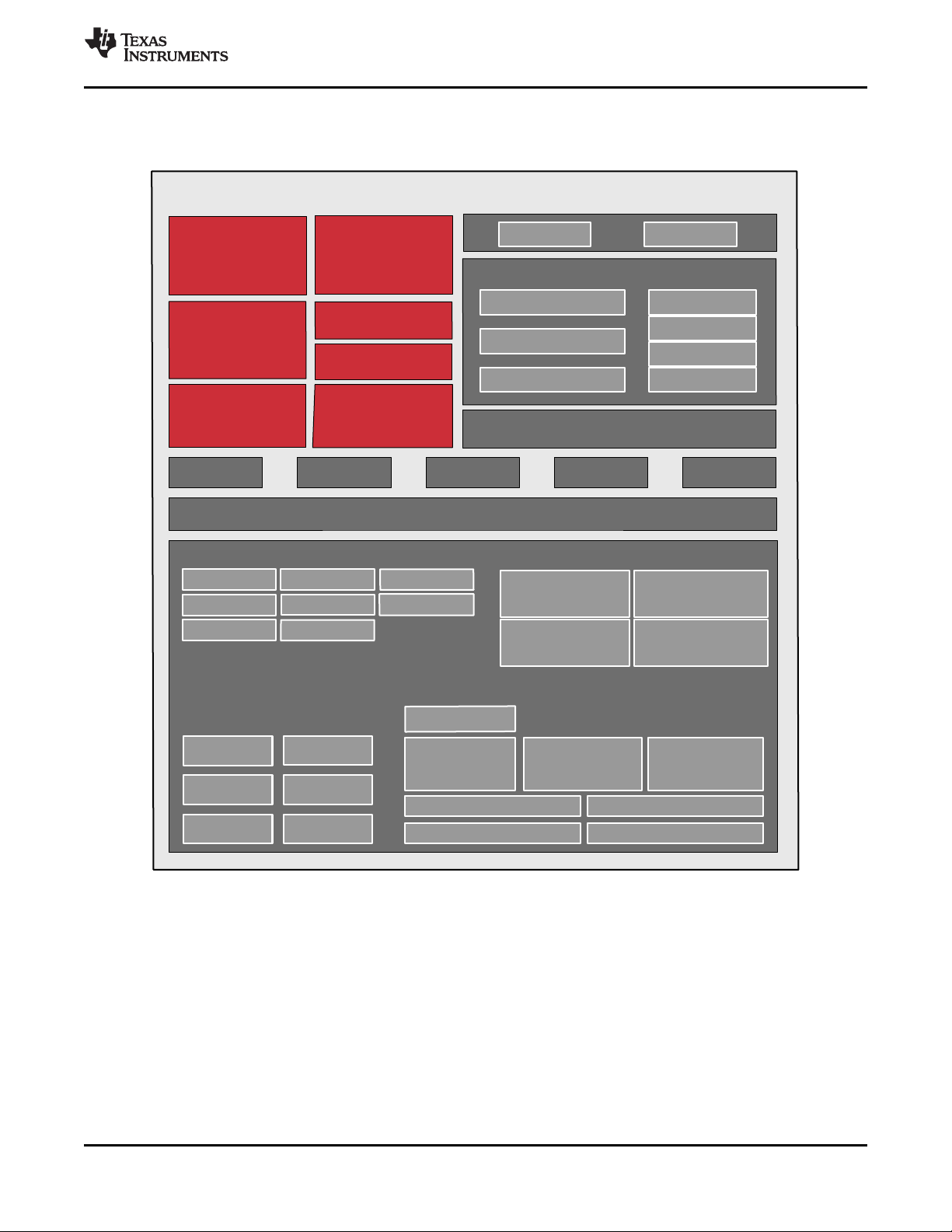
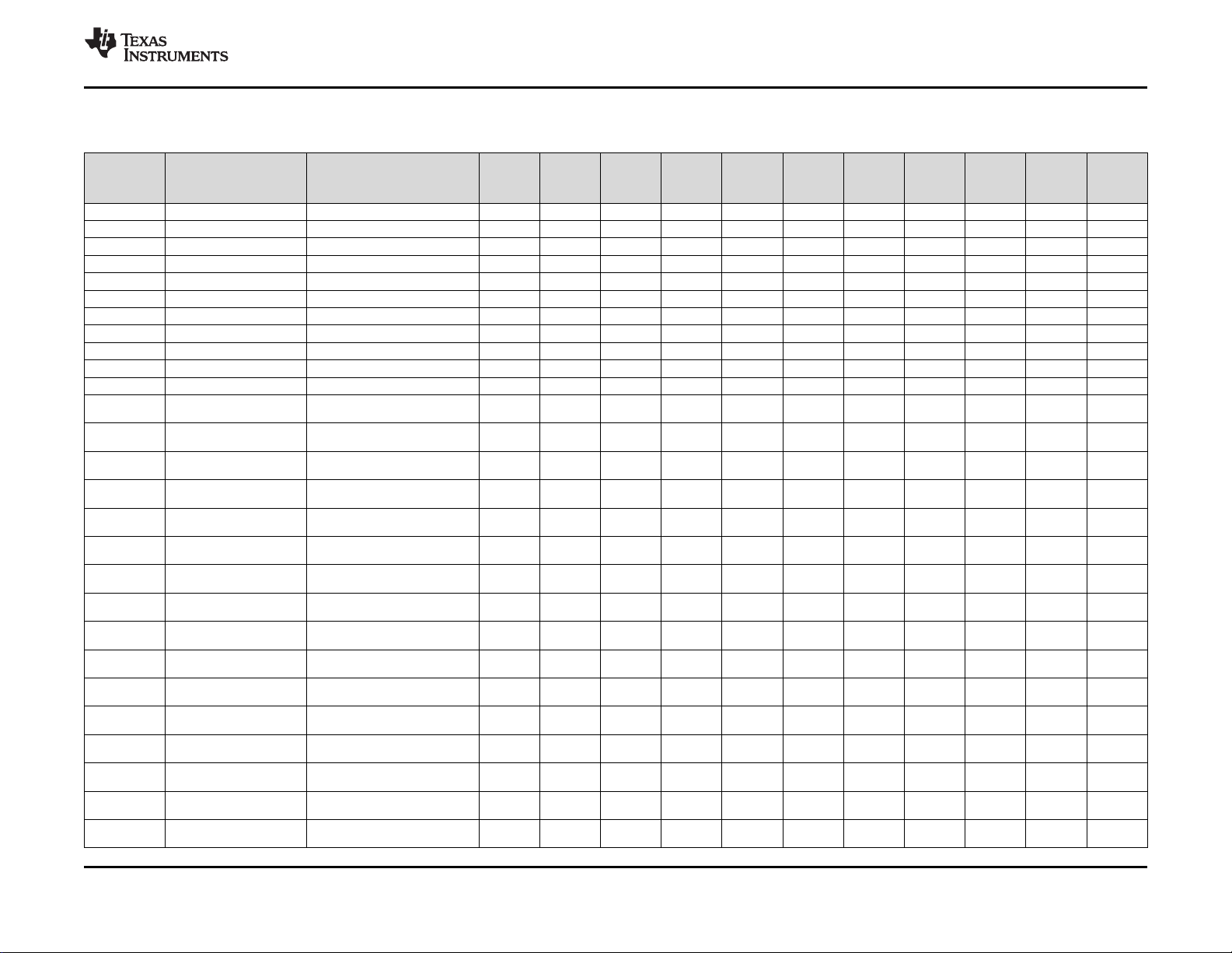
1.4 Functional Block Diagram
Figure 1-1 is functional block diagram for the device.
TDA2EG
SPRS958H –MARCH 2016–REVISED NOVEMBER 2019
Figure 1-1. TDA2Ex Block Diagram
Submit Documentation Feedback
Product Folder Links: TDA2EG
Device OverviewCopyright © 2016–2019, Texas Instruments Incorporated
3
TDA2EG
SPRS958H –MARCH 2016–REVISED NOVEMBER 2019
www.ti.com
Table of Contents
1 Device Overview ......................................... 1
1.1 Features .............................................. 1
1.2 Applications........................................... 2
1.3 Description............................................ 2
1.4 Functional Block Diagram ........................... 3
2 Revision History ......................................... 5
3 Device Comparison ..................................... 6
3.1 Related Products ..................................... 7
4 Terminal Configuration and Functions.............. 8
4.1 Terminal Assignment ................................. 8
4.2 Ball Characteristics ................................... 9
4.3 Multiplexing Characteristics ......................... 69
4.4 Signal Descriptions.................................. 85
5 Specifications ......................................... 121
5.1 Absolute Maximum Ratings........................ 121
5.2 ESD Ratings ....................................... 123
5.3 Power-On-Hour (POH) Limits...................... 123
5.4 Recommended Operating Conditions ............. 123
5.5 Operating Performance Points..................... 127
5.6 Power Consumption Summary .................... 147
5.7 Electrical Characteristics........................... 147
5.8 VPP Specifications for One-Time Programmable
(OTP) eFuses...................................... 157
5.9 Thermal Characteristics............................ 158
5.10 Power Supply Sequences ......................... 159
6 Clock Specifications ................................. 168
6.1 Input Clock Specifications ......................... 169
6.2 DPLLs, DLLs Specifications ....................... 178
7 Timing Requirements and Switching
Characteristics ........................................ 182
7.1 Timing Test Conditions ............................ 182
7.2 Interface Clock Specifications ..................... 182
7.3 Timing Parameters and Information ............... 182
7.4 Recommended Clock and Control Signal Transition
Behavior............................................ 184
7.5 Virtual and Manual I/O Timing Modes ............. 184
7.6 Video Input Ports (VIP) ............................ 186
7.7 Display Subsystem - Video Output Ports.......... 205
7.8 Display Subsystem - High-Definition Multimedia
Interface (HDMI) ................................... 216
7.9 Camera Serial Interface 2 CAL bridge (CSI2) ..... 217
7.10 External Memory Interface (EMIF)................. 217
7.11 General-Purpose Memory Controller (GPMC)..... 217
7.12 Timers.............................................. 241
7.13 Inter-Integrated Circuit Interface (I2C)............. 241
7.14 Universal Asynchronous Receiver Transmitter
(UART)............................................. 244
7.15 Multichannel Serial Peripheral Interface (McSPI) . 246
7.16 Quad Serial Peripheral Interface (QSPI) .......... 252
7.17 Multichannel Audio Serial Port (McASP) .......... 256
7.18 Universal Serial Bus (USB) ........................ 276
7.19 Serial Advanced Technology Attachment (SATA). 277
7.20 Peripheral Component Interconnect Express
(PCIe) .............................................. 278
7.21 Controller Area Network Interface (DCAN) ........ 278
7.22 Ethernet Interface (GMAC_SW) ................... 279
7.23 eMMC/SD/SDIO ................................... 292
7.24 General-Purpose Interface (GPIO) ................ 315
7.25 System and Miscellaneous interfaces ............. 316
7.26 Test Interfaces ..................................... 316
8 Applications, Implementation, and Layout ...... 320
8.1 Introduction ........................................ 320
8.2 Power Optimizations............................... 321
8.3 Core Power Domains .............................. 332
8.4 Single-Ended Interfaces ........................... 343
8.5 Differential Interfaces .............................. 345
8.6 Clock Routing Guidelines.......................... 365
8.7 DDR3 Board Design and Layout Guidelines....... 366
9 Device and Documentation Support.............. 390
9.1 Device Nomenclature and Orderable Information . 390
9.2 Tools and Software ................................ 392
9.3 Documentation Support............................ 393
9.4 Support Resources ................................ 393
9.5 Trademarks ........................................ 393
9.6 Electrostatic Discharge Caution ................... 394
9.7 Glossary............................................ 394
10 Mechanical, Packaging, and Orderable
Information............................................. 395
10.1 Packaging Information ............................. 395
4
Table of Contents Copyright © 2016–2019, Texas Instruments Incorporated
Submit Documentation Feedback
Product Folder Links: TDA2EG

TDA2EG
www.ti.com
SPRS958H –MARCH 2016–REVISED NOVEMBER 2019
2 Revision History
Changes from June 8, 2018 to February 15, 2019 (from F Revision (June 2018) to G Revision) Page
• Added Device Security Features for Silicon revision 2.1 in Section 1.1, Features........................................... 1
• Added clarification note regarding XDRA726 part number in Table 3-1, Device Comparison ............................. 6
• Added vpp details for Silicon revision 2.1 in Table 4-1, Unused Balls Specific Connection Requirements,
Table 4-2, Ball Characteristics and Table 4-31, Power Supply Signal Descriptions......................................... 9
• Updated porz, resetn and rstoutn signal descriptions in Table 4-26, PRCM Signal Descriptions ...................... 115
• Added clarification note regarding TSHUT feature in Table 5-4, Recommended Operating Conditions............... 127
• Updated OPP_HIGH power supply value in note (6) under Table 5-7, Voltage Domains Operating Performance
Points................................................................................................................................ 128
• Added missing RTC details in Table 5-8, Supported OPP vs Max Frequency and added Section 5.7.6, LVCMOS
OSC Buffers DC Electrical Characteristics..................................................................................... 128
• Updated SYS_32K to FUNC_32K_CLK in Table 5-9, Maximum Supported Frequency ................................ 129
• Added Section 5.8, VPP Specifications for One-Time Programmable (OTP) eFuses for Silicon revision 2.1 ........ 157
• Updated Section 5.10, Power Supply Sequences............................................................................. 159
• Updated system clock names in Section 6, Clock Specifications ........................................................... 168
• Added missing RTC details in Section 6, Clock Specifications.............................................................. 168
• Added Section 8.3.7, Loss of Input Power Event.............................................................................. 337
• Added Section 8.5.5, SATA Board Design and Layout Guidelines ........................................................ 359
• Added Section 8.6, Clock Routing Guidelines ................................................................................ 365
• Updated note for cosmetic marks on package................................................................................. 390
• Added Silicon revison 2.1 in support in Table 9-1, Nomenclature Description ............................................ 391
• Added clarification note regarding XDRA726 part number in Table 9-1, Nomenclature Description................... 391
Changes from February 16, 2019 to November 15, 2019 (from G Revision (February 2019) to H Revision) Page
• Updated note regarding XDRA726 part number in Table 3-1, Device Comparison ......................................... 7
• Added reminders to disable unused pulls and RX pads in Section 4.2, Ball Characteristics ............................. 10
• Removed uart2_rxd for Muxmode 0 .............................................................................................. 12
• Added clarification notes for EMU[1:0] connections in Table 4-22, GPIOs Signal Descriptions and Table 4-24,
Debug Signal Descriptions ....................................................................................................... 107
• Updated clock names in Table 5-9, Maximum Supported Frequency ...................................................... 129
• Updated EMIF_DLL_FCLK max rate in Table 6-15, DLL Characteristics.................................................. 181
• Updated GPMC timing table footnotes.......................................................................................... 218
• Updated timing specification values for GPMC and MMC ................................................................... 218
• Updated information about WD_TIMER1 in Section 7.12, Timers .......................................................... 241
• Updated parameter in Table 7-42, Timing Requirements for QSPI......................................................... 254
• Added MII_TXER timing to Section 7.22.1, GMAC MII Timings............................................................. 281
• Updated MDIO Timing Diagram and MDIO7 parameter values............................................................. 283
• Updated Delay time for MMC2 in Table 7-109, Switching Characteristics for MMC2 - JC64 High Speed DDR
Mode................................................................................................................................. 304
• Added note regarding DDR ECC solutions to Table 8-30, Supported DDR3 Device Combinations ................... 367
• Added clarifications about validated DDR topology ........................................................................... 376
• Updated note regarding XDRA726 part number in Table 9-1, Nomenclature Description............................... 392
Submit Documentation Feedback
Product Folder Links: TDA2EG
Revision HistoryCopyright © 2016–2019, Texas Instruments Incorporated
5
TDA2EG
SPRS958H –MARCH 2016–REVISED NOVEMBER 2019
3 Device Comparison
Table 3-1 shows a comparison between devices, highlighting the differences.
www.ti.com
Table 3-1. Device Comparison
FEATURES
Features
CTRL_WKUP_STD_FUSE_DIE_ID_2[31:24] Base PN register bit field value
Processors/Accelerators
Speed Grades H, D
Arm Single Cortex-A15 Microprocessor (MPU) Subsystem MPU core 0 Yes
C66x VLIW DSP DSP1 Yes
BitBLT 2D Hardware Acceleration Engine (BB2D) BB2D Yes
Display Subsystem
Dual Arm Cortex-M4 Image Processing Unit (IPU)
Image Video Accelarator (IVA) IVA Yes
SGX544 Single-Core 3D Graphics Processing Unit (GPU) GPU Yes
Video Input Port (VIP) VIP1
Video Processing Engine (VPE) VPE Yes
Program/Data Storage
On-Chip Shared Memory (RAM) OCMC_RAM1 512KB
General-Purpose Memory Controller (GPMC) GPMC Yes
DDR3 Memory Controller
Dynamic Memory Manager (DMM) DMM Yes
Peripherals
Dual Controller Area Network (DCAN) Interface
Enhanced DMA (EDMA) EDMA Yes
System DMA (DMA_SYSTEM) DMA_SYSTEM Yes
Ethernet Subsystem (Ethernet SS)
General-Purpose I/O (GPIO) GPIO up to 215
Inter-Integrated Circuit (I2C) Interface I2C 6
System Mailbox Module MAILBOX 13
Camera Adaptation Layer (CAL) Camera Serial Interface 2 (CSI2)
(1)(2)
VOUT1 Yes
VOUT2 Yes
VOUT3 Yes
HDMI Yes
IPU1 Yes
IPU2 Yes
vin1a Yes
vin1b Yes
vin2a Yes
vin2b Yes
EMIF1 up to 2GB across single chip select
SECDED/ECC Yes
DCAN1 Yes
DCAN2 Yes
GMAC_SW[0] MII, RMII, or RGMII
GMAC_SW[1] MII, RMII, or RGMII
CSI2_0 1 CLK + 4 Data Line
CSI2_1 1 CLK + 2 Data Line
(2)
DEVICE
TDA2EG
TDA2EGx: 20 (0x14)
6
Device Comparison Copyright © 2016–2019, Texas Instruments Incorporated
Submit Documentation Feedback
Product Folder Links: TDA2EG

www.ti.com
TDA2EG
SPRS958H –MARCH 2016–REVISED NOVEMBER 2019
Table 3-1. Device Comparison
FEATURES
McASP1 16 serializers
McASP2 16 serializers
McASP3 4 serializers
Multichannel Audio Serial Port (McASP)
MultiMedia Card/Secure Digital/Secure Digital Input Output Interface
(MMC/SD/SDIO)
PCI-Express 3.0 Port with Integrated PHY
Serial Advanced Technology Attachment (SATA) SATA Yes
Real-Time Clock Subsystem (RTCSS) RTCSS Yes
Multichannel Serial Peripheral Interface (McSPI) McSPI 4
Quad SPI (QSPI) QSPI Yes
Spinlock Module SPINLOCK Yes
Timers, General-Purpose TIMERS GP 16
Timer, Watchdog WD TIMER Yes
Pulse-Width Modulation Subsystem (PWMSS)
Universal Asynchronous Receiver/Transmitter (UART) UART 10
Universal Serial Bus (USB3.0)
Universal Serial Bus (USB2.0)
(1) For more details about the CTRL_WKUP_STD_FUSE_DIE_ID_2 register and Base PN bit field, see the TDA2Ex Technical Reference
Manual.
(2) XDRA726 base part number with X speed grade indicator is the part number for the superset device. Software should constrain the
features and speed used to match the intended production device. The Base PN register bit field value is 0x4.
McASP4 4 serializers
McASP5 4 serializers
McASP6 4 serializers
McASP7 4 serializers
McASP8 4 serializers
MMC1 1x UHSI 4b
MMC2 1x eMMC™ 8b
MMC3 1x SDIO 8b
MMC4 1x SDIO 4b
PCIe_SS1 Yes
PCIe_SS2 Yes
PWMSS1 Yes
PWMSS2 Yes
PWMSS3 Yes
USB1 (SuperSpeed, DualRole-Device [DRD])
USB2 (High Speed, DualRole-Device [DRD], with
embedded HS PHY)
USB3 (High Speed, OTG2.0,
with ULPI)
USB4 (High Speed, OTG2.0,
with ULPI)
(2)
(continued)
DEVICE
TDA2EG
Yes
Yes
Yes
No
3.1 Related Products
Automotive Processors
TDAx ADAS SoCs TI's TDAx Driver Assistance System-on-Chip (SoC) family offers scalable and open
solutions and a common hardware and software architecture for Advanced Driver Assistance
Systems (ADAS) applications including camera-based front (mono and stereo), rear,
surround view and night vision systems, and mid- and long-range radar and sensor fusion
systems.
Companion Products for TDAx Review products that are frequently purchased or used in conjunction
with this product.
Submit Documentation Feedback
Product Folder Links: TDA2EG
Device ComparisonCopyright © 2016–2019, Texas Instruments Incorporated
7
SPRS906_BALL_01
TDA2EG
SPRS958H –MARCH 2016–REVISED NOVEMBER 2019
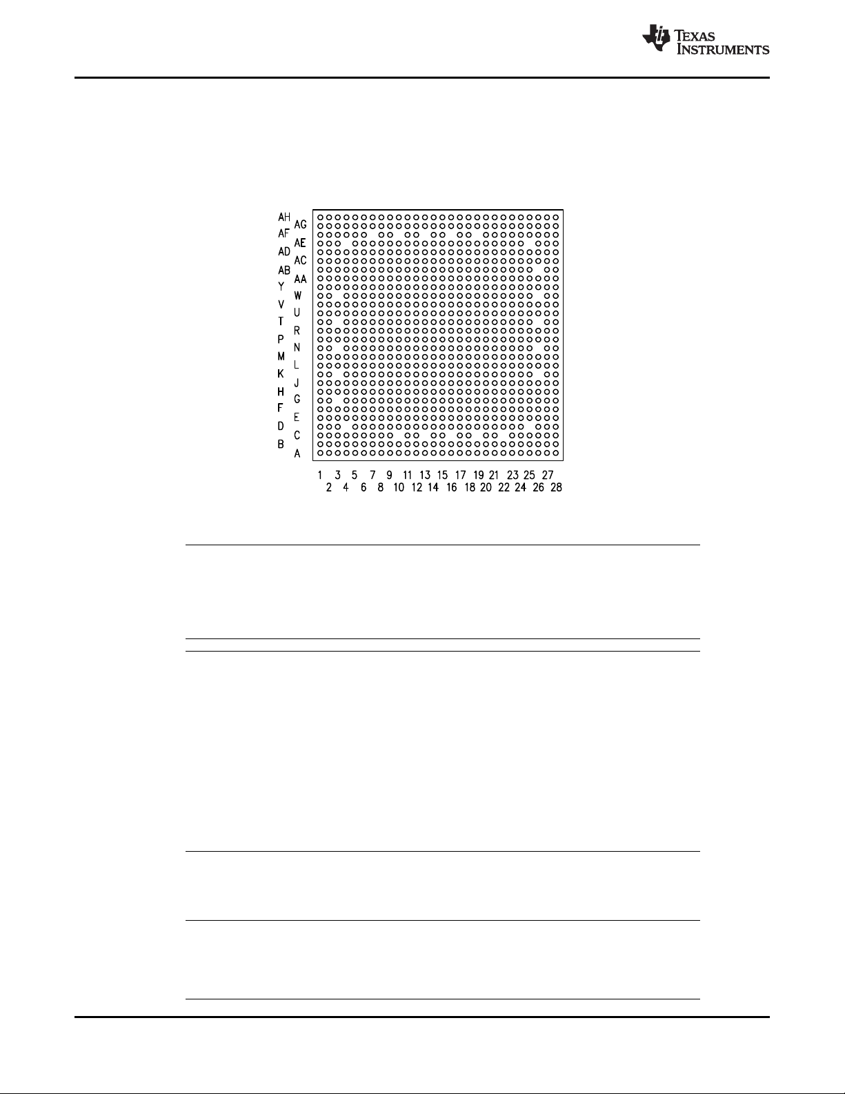
4 Terminal Configuration and Functions
4.1 Terminal Assignment
Figure 4-1 shows the ball locations for the 760 plastic ball grid array (PBGA) package and is used in
conjunction with Table 4-2 through Table 4-31 to locate signal names and ball grid numbers.
www.ti.com
Figure 4-1. ABC S-PBGA-N760 Package (Bottom View)
The following bottom balls are not pinned out: AF7, AF10, AF13, AF16, AF19, AE4, AE25,
AB26, W3, W26, T3, T26, N3, N26, K3, K26, G3, D4, D25, C10, C13, C16, C19, C22.
These balls do not exist on the package.
The following bottom balls are not connected: AH11, AH12, AG2, AG8, AG11, AG12, AF4,
AF6, AF8, AF9, AE3, AE5, AE6, AE8, AE9, AD3, AD8, AD9, Y15, Y16, V18, V19, U18, U19,
U22, U23, U24, U25, U26, U27, U28, T22, T23, T27, T28, R20, R22, R23, R24, R25, R26,
R27, R28, P19, P22, P23, P24, P25, P26, P27, N20, N22, N23, N27, N28, M20, M21, M22,
M23, M24, M25, M26, M27, M28, L20, L21, L22, L23, L24, L25, L26, L27, L28, K20, K21,
K22, K23, K27, K28, J20, J21, J22, J23, J24, J25, J26, J27, H20, H21, H22, H23, H24, H25,
H26, H27, H28, G22, G23, G24, G25, G26, G27, G28, F24, F25, F26, F27, F28, E24, E26,
E27, E28
These balls can be connected as desired, including to VSS. For users designing TDA2x
compatible PCB, please refer to TDA2x Data Manual for appropriate requirements.
4.1.1 Unused Balls Connection Requirements
This section describes the connection requirements of the unused and reserved balls.
NOTE
NOTE
NOTE
The following balls are reserved: A27, Y5, Y10, B28, AC1, AC2, AA1, AA2, AB1, AB2, AD14.
These balls must be left unconnected.
8
Terminal Configuration and Functions Copyright © 2016–2019, Texas Instruments Incorporated
Submit Documentation Feedback
Product Folder Links: TDA2EG
www.ti.com
All unused power supply balls must be supplied with the voltages specified in the
Section 5.4, Recommended Operating Conditions, unless alternative tie-off options are
included in Section 4.4, Signal Descriptions.
Table 4-1. Unused Balls Specific Connection Requirements
BALLS CONNECTION REQUIREMENTS
AE15, AC15, AE14, D20, AD17, AC16, V27, AH25, AE27, AD27,
Y28
E20, D21, E23, C20, C21, V28, F18, AG25, AE28, AD28, Y27, F17,
C25
K14 (vpp) This ball must be left unconnected if unused
AF14 (rtc_iso)
AB17 (rtc_porz)
TDA2EG
SPRS958H –MARCH 2016–REVISED NOVEMBER 2019
NOTE
These balls must be connected to GND through an external pull
resistor if unused.
These balls must be connected to the corresponding power supply
through an external pull resistor if unused.
This ball should be connected to the corresponding power supply
through an external pull resistor if unused; or can be connected to
F22 (porz) when RTC unused (level translation may be needed)
This ball should be connected to VSS when RTC is unused; or can
be connected to F22 (porz) when RTC unused (level translation may
be needed)
All other unused signal balls with a Pad Configuration register can be left unconnected with
their internal pullup or pulldown resistor enabled.
All other unused signal balls without a Pad Configuration register can be left unconnected.
4.2 Ball Characteristics
Table 4-2 describes the terminal characteristics and the signals multiplexed on each ball. The following list
describes the table column headers:
1. BALL NUMBER:This column lists ball numbers on the bottom side associated with each signal on the
bottom.
2. BALL NAME: This column lists mechanical name from package device (name is taken from muxmode
0).
3. SIGNAL NAME:This column lists names of signals multiplexed on each ball (also notice that the name
of the ball is the signal name in muxmode 0).
Table 4-2 does not take into account the subsystem multiplexing signals. Subsystem
multiplexing signals are described in Section 4.4, Signal Descriptions.
NOTE
NOTE
NOTE
NOTE
In driver off mode, the buffer is configured in high-impedance.
Submit Documentation Feedback
Product Folder Links: TDA2EG
Terminal Configuration and FunctionsCopyright © 2016–2019, Texas Instruments Incorporated
9
TDA2EG
SPRS958H –MARCH 2016–REVISED NOVEMBER 2019
In some cases Table 4-2 may present more than one signal name per muxmode for the
same ball. First signal in the list is the dominant function as selected via
CTRL_CORE_PAD_* register.
All other signals are virtual functions that present alternate multiplexing options. This virtual
functions are controlled via CTRL_CORE_ALT_SELECT_MUX or
CTRL_CORE_VIP_MUX_SELECT register. For more information on how to use these
options, see Pad Configuration Registers section, Control Module chapter in the device TRM.
4. MUXMODE: Multiplexing mode number:
a. MUXMODE 0 is the primary mode; this means that when MUXMODE=0 is set, the function
mapped on the pin corresponds to the name of the pin. The primary muxmode is not necessarily
the default muxmode.
The default mode is the mode at the release of the reset; also see the RESET REL.
MUXMODE column.
b. MUXMODE 1 through 15 are possible muxmodes for alternate functions. On each pin, some
muxmodes are effectively used for alternate functions, while some muxmodes are not used. Only
MUXMODE values which correspond to defined functions should be used.
c. An empty box means Not Applicable.
5. TYPE: Signal type and direction:
– I = Input
– O = Output
– IO = Input or Output
– D = Open drain
– DS = Differential Signaling
– A = Analog
– PWR = Power
– GND = Ground
– CAP = LDO Capacitor
www.ti.com
NOTE
NOTE
10
NOTE
The RX buffer within the pad logic should be disabled on all pins that are not being used as
an input. For more information, see the Control Module / Control Module Functional
Description / PAD Functional Multiplexing and Configuration section in the device TRM.
6. BALL RESET STATE: The state of the terminal at power-on reset:
– drive 0 (OFF): The buffer drives VOL(pulldown or pullup resistor not activated)
– drive 1 (OFF): The buffer drives VOH(pulldown or pullup resistor not activated)
– OFF: High-impedance
– PD: High-impedance with an active pulldown resistor
– PU: High-impedance with an active pullup resistor
– An empty box means Not Applicable
NOTE
Designs that contain pullup or pulldown resistors, either on the board or in attached devices
that oppose internal pullup or pulldown resistors, that are active while the device is held in
reset, must not remain in reset for long periods of time.
7. BALL RESET REL. STATE: The state of the terminal at the deactivation of the rstoutn signal (also
Terminal Configuration and Functions Copyright © 2016–2019, Texas Instruments Incorporated
Submit Documentation Feedback
Product Folder Links: TDA2EG
www.ti.com
8. BALL RESET REL. MUXMODE: This muxmode is automatically configured at the release of the
9. IO VOLTAGE VALUE: This column describes the IO voltage value (VDDS supply).
10. POWER: The voltage supply that powers the terminal IO buffers.
11. HYS: Indicates if the input buffer is with hysteresis:
TDA2EG
SPRS958H –MARCH 2016–REVISED NOVEMBER 2019
mapped to the PRCM SYS_WARM_OUT_RST signal)
– drive 0 (OFF): The buffer drives VOL(pulldown or pullup resistor not activated)
– drive clk (OFF): The buffer drives a toggling clock (pulldown or pullup resistor not activated)
– drive 1 (OFF): The buffer drives VOH(pulldown or pullup resistor not activated)
– OFF: High-impedance
– PD: High-impedance with an active pulldown resistor
– PU: High-impedance with an active pullup resistor
– An empty box means Not Applicable
NOTE
For more information on the CORE_PWRON_RET_RST reset signal and its reset sources,
see Power, Reset, and Clock Management chapter in the device TRM.
rstoutn signal (also mapped to the PRCM SYS_WARM_OUT_RST signal).
An empty box means Not Applicable.
An empty box means Not Applicable.
An empty box means Not Applicable.
– Yes: With hysteresis
– No: Without hysteresis
– An empty box: Not Applicable
NOTE
For more information, see the hysteresis values in Section 5.7, Electrical Characteristics.
12. BUFFER TYPE: Drive strength of the associated output buffer.
An empty box means Not Applicable.
NOTE
For programmable buffer strength:
– The default value is given in Table 4-2.
– A note describes all possible values according to the selected muxmode.
13. PULLUP / PULLDOWN TYPE: Denotes the presence of an internal pullup or pulldown resistor.
Pullup and pulldown resistors can be enabled or disabled via software.
– PU: Internal pullup
– PD: Internal pulldown
– PU/PD: Internal pullup and pulldown
– PUx/PDy: Programmable internal pullup and pulldown
– PDy: Programmable internal pulldown
– An empty box means No pull
NOTE
Internal pullup or pulldown resistors must be disabled when opposed by an external pullup or
pulldown resistor on the board or within an attached device.
14. DSIS: The deselected input state (DSIS) indicates the state driven on the peripheral input (logic "0" or
logic "1") when the peripheral pin function is not selected by any of the PINCNTLx registers.
– 0: Logic 0 driven on the peripheral's input signal port.
Terminal Configuration and FunctionsCopyright © 2016–2019, Texas Instruments Incorporated
Submit Documentation Feedback
Product Folder Links: TDA2EG
11
TDA2EG
SPRS958H –MARCH 2016–REVISED NOVEMBER 2019
– 1: Logic 1 driven on the peripheral's input signal port.
– blank: Pin state driven on the peripheral's input signal port.
Configuring two pins to the same input signal is not supported as it can yield unexpected
results. This can be easily prevented with the proper software configuration (Hi-Z mode is not
an input signal).
When a pad is set into a multiplexing mode which is not defined by pin multiplexing, that
pad’s behavior is undefined. This should be avoided.
Some of the EMIF1 signals have an additional state change at the release of porz. The state
that the signals change to at the release of porz is as follows:
drive 0 (OFF) for: ddr1_csn0, ddr1_ck, ddr1_nck, ddr1_casn, ddr1_rasn, ddr1_wen,
ddr1_ba[2:0], ddr1_a[15:0].
OFF for: ddr1_ecc_d[7:0], ddr1_dqm[3:0], ddr1_dqm_ecc, ddr1_dqs[3:0], ddr1_dqsn[3:0],
ddr1_dqs_ecc, ddr1_dqsn_ecc, ddr1_d[31:0].
www.ti.com
NOTE
NOTE
NOTE
NOTE
Dual rank support is not available on this device, but signal names are retained for
consistency with the TDA2xx family of devices.
12
Terminal Configuration and Functions Copyright © 2016–2019, Texas Instruments Incorporated
Submit Documentation Feedback
Product Folder Links: TDA2EG
www.ti.com
TDA2EG
SPRS958H –MARCH 2016–REVISED NOVEMBER 2019
BALL
(1)
BALL
RESET REL.
MUXMODE
[8]
I/O
VOLTAGE
VALUE [9]
POWER [10] HYS [11]
BUFFER
TYPE [12]
CSI2
CSI2
CSI2
CSI2
CSI2
CSI2
CSI2
CSI2
CSI2
CSI2
CSI2
CSI2
CSI2
CSI2
CSI2
CSI2
Table 4-2. Ball Characteristics
BALL NUMBER
[1]
K9 cap_vbbldo_dsp cap_vbbldo_dsp CAP
Y14 cap_vbbldo_gpu cap_vbbldo_gpu CAP
J10 cap_vbbldo_iva cap_vbbldo_iva CAP
J16 cap_vbbldo_mpu cap_vbbldo_mpu CAP
T20 cap_vddram_core1 cap_vddram_core1 CAP
L9 cap_vddram_core3 cap_vddram_core3 CAP
J19 cap_vddram_core4 cap_vddram_core4 CAP
J9 cap_vddram_dsp cap_vddram_dsp CAP
Y13 cap_vddram_gpu cap_vddram_gpu CAP
K16 cap_vddram_iva cap_vddram_iva CAP
K19 cap_vddram_mpu cap_vddram_mpu CAP
AE1 csi2_0_dx0 csi2_0_dx0 0 I 1.8 vdda_csi Yes LVCMOS
AF1 csi2_0_dx1 csi2_0_dx1 0 I 1.8 vdda_csi Yes LVCMOS
AF2 csi2_0_dx2 csi2_0_dx2 0 I 1.8 vdda_csi Yes LVCMOS
AH4 csi2_0_dx3 csi2_0_dx3 0 I 1.8 vdda_csi Yes LVCMOS
AH3 csi2_0_dx4 csi2_0_dx4 0 I 1.8 vdda_csi Yes LVCMOS
AD2 csi2_0_dy0 csi2_0_dy0 0 I 1.8 vdda_csi Yes LVCMOS
AE2 csi2_0_dy1 csi2_0_dy1 0 I 1.8 vdda_csi Yes LVCMOS
AF3 csi2_0_dy2 csi2_0_dy2 0 I 1.8 vdda_csi Yes LVCMOS
AG4 csi2_0_dy3 csi2_0_dy3 0 I 1.8 vdda_csi Yes LVCMOS
AG3 csi2_0_dy4 csi2_0_dy4 0 I 1.8 vdda_csi Yes LVCMOS
AG5 csi2_1_dx0 csi2_1_dx0 0 I 1.8 vdda_csi Yes LVCMOS
AG6 csi2_1_dx1 csi2_1_dx1 0 I 1.8 vdda_csi Yes LVCMOS
AH7 csi2_1_dx2 csi2_1_dx2 0 I 1.8 vdda_csi Yes LVCMOS
AH5 csi2_1_dy0 csi2_1_dy0 0 I 1.8 vdda_csi Yes LVCMOS
AH6 csi2_1_dy1 csi2_1_dy1 0 I 1.8 vdda_csi Yes LVCMOS
AG7 csi2_1_dy2 csi2_1_dy2 0 I 1.8 vdda_csi Yes LVCMOS
BALL NAME [2] SIGNAL NAME [3]
MUXMODE
[4]
TYPE [5]
BALL
RESET
STATE [6]
RESET REL.
STATE [7]
PULL
UP/DOWN
TYPE [13]
PU/PD
PU/PD
PU/PD
PU/PD
PU/PD
PU/PD
PU/PD
PU/PD
PU/PD
PU/PD
PU/PD
PU/PD
PU/PD
PU/PD
PU/PD
PU/PD
DSIS [14]
Copyright © 2016–2019, Texas Instruments Incorporated Terminal Configuration and Functions
Submit Documentation Feedback
Product Folder Links: TDA2EG
13
TDA2EG
SPRS958H –MARCH 2016–REVISED NOVEMBER 2019
www.ti.com
Table 4-2. Ball Characteristics
BALL NUMBER
[1]
G19 dcan1_rx dcan1_rx 0 IO PU PU 15 1.8/3.3 vddshv3 Yes Dual Voltage
G20 dcan1_tx dcan1_tx 0 IO PU PU 15 1.8/3.3 vddshv3 Yes Dual Voltage
AD20 ddr1_a0 ddr1_a0 0 O PD drive 1 (OFF) 1.35/1.5 vdds_ddr1 No LVCMOS
AC19 ddr1_a1 ddr1_a1 0 O PD drive 1 (OFF) 1.35/1.5 vdds_ddr1 No LVCMOS
AC20 ddr1_a2 ddr1_a2 0 O PD drive 1 (OFF) 1.35/1.5 vdds_ddr1 No LVCMOS
AB19 ddr1_a3 ddr1_a3 0 O PD drive 1 (OFF) 1.35/1.5 vdds_ddr1 No LVCMOS
AF21 ddr1_a4 ddr1_a4 0 O PD drive 1 (OFF) 1.35/1.5 vdds_ddr1 No LVCMOS
AH22 ddr1_a5 ddr1_a5 0 O PD drive 1 (OFF) 1.35/1.5 vdds_ddr1 No LVCMOS
AG23 ddr1_a6 ddr1_a6 0 O PD drive 1 (OFF) 1.35/1.5 vdds_ddr1 No LVCMOS
AE21 ddr1_a7 ddr1_a7 0 O PD drive 1 (OFF) 1.35/1.5 vdds_ddr1 No LVCMOS
AF22 ddr1_a8 ddr1_a8 0 O PD drive 1 (OFF) 1.35/1.5 vdds_ddr1 No LVCMOS
AE22 ddr1_a9 ddr1_a9 0 O PD drive 1 (OFF) 1.35/1.5 vdds_ddr1 No LVCMOS
AD21 ddr1_a10 ddr1_a10 0 O PD drive 1 (OFF) 1.35/1.5 vdds_ddr1 No LVCMOS
AD22 ddr1_a11 ddr1_a11 0 O PD drive 1 (OFF) 1.35/1.5 vdds_ddr1 No LVCMOS
AC21 ddr1_a12 ddr1_a12 0 O PD drive 1 (OFF) 1.35/1.5 vdds_ddr1 No LVCMOS
AF18 ddr1_a13 ddr1_a13 0 O PD drive 1 (OFF) 1.35/1.5 vdds_ddr1 No LVCMOS
AE17 ddr1_a14 ddr1_a14 0 O PD drive 1 (OFF) 1.35/1.5 vdds_ddr1 No LVCMOS
BALL NAME [2] SIGNAL NAME [3]
uart8_txd 2 O
mmc2_sdwp 3 I 0
sata1_led 4 O
hdmi1_cec 6 IO
gpio1_15 14 IO
Driver off 15 I
uart8_rxd 2 I 1
mmc2_sdcd 3 I 1
hdmi1_hpd 6 IO
gpio1_14 14 IO
Driver off 15 I
MUXMODE
[4]
TYPE [5]
BALL
RESET
STATE [6]
(1)
(continued)
BALL
RESET REL.
STATE [7]
BALL
RESET REL.
MUXMODE
[8]
I/O
VOLTAGE
VALUE [9]
POWER [10] HYS [11]
BUFFER
TYPE [12]
LVCMOS
LVCMOS
DDR
DDR
DDR
DDR
DDR
DDR
DDR
DDR
DDR
DDR
DDR
DDR
DDR
DDR
DDR
PULL
UP/DOWN
TYPE [13]
PU/PD 1
PU/PD 1
PUx/PDy
PUx/PDy
PUx/PDy
PUx/PDy
PUx/PDy
PUx/PDy
PUx/PDy
PUx/PDy
PUx/PDy
PUx/PDy
PUx/PDy
PUx/PDy
PUx/PDy
PUx/PDy
PUx/PDy
DSIS [14]
14
Copyright © 2016–2019, Texas Instruments IncorporatedTerminal Configuration and Functions
Submit Documentation Feedback
Product Folder Links: TDA2EG

www.ti.com
TDA2EG
SPRS958H –MARCH 2016–REVISED NOVEMBER 2019
Table 4-2. Ball Characteristics
BALL NUMBER
[1]
AD18 ddr1_a15 ddr1_a15 0 O PD drive 1 (OFF) 1.35/1.5 vdds_ddr1 No LVCMOS
AF17 ddr1_ba0 ddr1_ba0 0 O PU drive 1 (OFF) 1.35/1.5 vdds_ddr1 No LVCMOS
AE18 ddr1_ba1 ddr1_ba1 0 O PU drive 1 (OFF) 1.35/1.5 vdds_ddr1 No LVCMOS
AB18 ddr1_ba2 ddr1_ba2 0 O PU drive 1 (OFF) 1.35/1.5 vdds_ddr1 No LVCMOS
AC18 ddr1_casn ddr1_casn 0 O PU drive 1 (OFF) 1.35/1.5 vdds_ddr1 No LVCMOS
AG24 ddr1_ck ddr1_ck 0 O PD drive 0 (OFF) 1.35/1.5 vdds_ddr1 No LVCMOS
AG22 ddr1_cke ddr1_cke 0 O PU drive 1 (OFF) 1.35/1.5 vdds_ddr1 No LVCMOS
AH23 ddr1_csn0 ddr1_csn0 0 O PU drive 1 (OFF) 1.35/1.5 vdds_ddr1 No LVCMOS
AB16 ddr1_csn1 ddr1_csn1 0 O PU drive 1 (OFF) 1.35/1.5 vdds_ddr1 No LVCMOS
AF25 ddr1_d0 ddr1_d0 0 IO PD PD 1.35/1.5 vdds_ddr1 No LVCMOS
AF26 ddr1_d1 ddr1_d1 0 IO PD PD 1.35/1.5 vdds_ddr1 No LVCMOS
AG26 ddr1_d2 ddr1_d2 0 IO PD PD 1.35/1.5 vdds_ddr1 No LVCMOS
AH26 ddr1_d3 ddr1_d3 0 IO PD PD 1.35/1.5 vdds_ddr1 No LVCMOS
AF24 ddr1_d4 ddr1_d4 0 IO PD PD 1.35/1.5 vdds_ddr1 No LVCMOS
AE24 ddr1_d5 ddr1_d5 0 IO PD PD 1.35/1.5 vdds_ddr1 No LVCMOS
AF23 ddr1_d6 ddr1_d6 0 IO PD PD 1.35/1.5 vdds_ddr1 No LVCMOS
AE23 ddr1_d7 ddr1_d7 0 IO PD PD 1.35/1.5 vdds_ddr1 No LVCMOS
AC23 ddr1_d8 ddr1_d8 0 IO PD PD 1.35/1.5 vdds_ddr1 No LVCMOS
AF27 ddr1_d9 ddr1_d9 0 IO PD PD 1.35/1.5 vdds_ddr1 No LVCMOS
AG27 ddr1_d10 ddr1_d10 0 IO PD PD 1.35/1.5 vdds_ddr1 No LVCMOS
AF28 ddr1_d11 ddr1_d11 0 IO PD PD 1.35/1.5 vdds_ddr1 No LVCMOS
AE26 ddr1_d12 ddr1_d12 0 IO PD PD 1.35/1.5 vdds_ddr1 No LVCMOS
AC25 ddr1_d13 ddr1_d13 0 IO PD PD 1.35/1.5 vdds_ddr1 No LVCMOS
BALL NAME [2] SIGNAL NAME [3]
MUXMODE
[4]
TYPE [5]
BALL
RESET
STATE [6]
(1)
(continued)
BALL
RESET REL.
STATE [7]
BALL
RESET REL.
MUXMODE
[8]
I/O
VOLTAGE
VALUE [9]
POWER [10] HYS [11]
BUFFER
TYPE [12]
DDR
DDR
DDR
DDR
DDR
DDR
DDR
DDR
DDR
DDR
DDR
DDR
DDR
DDR
DDR
DDR
DDR
DDR
DDR
DDR
DDR
DDR
DDR
PULL
UP/DOWN
TYPE [13]
PUx/PDy
PUx/PDy
PUx/PDy
PUx/PDy
PUx/PDy
PUx/PDy
PUx/PDy
PUx/PDy
PUx/PDy
PUx/PDy
PUx/PDy
PUx/PDy
PUx/PDy
PUx/PDy
PUx/PDy
PUx/PDy
PUx/PDy
PUx/PDy
PUx/PDy
PUx/PDy
PUx/PDy
PUx/PDy
PUx/PDy
DSIS [14]
Copyright © 2016–2019, Texas Instruments Incorporated Terminal Configuration and Functions
Submit Documentation Feedback
Product Folder Links: TDA2EG
15

TDA2EG
SPRS958H –MARCH 2016–REVISED NOVEMBER 2019
www.ti.com
Table 4-2. Ball Characteristics
BALL NUMBER
[1]
AC24 ddr1_d14 ddr1_d14 0 IO PD PD 1.35/1.5 vdds_ddr1 No LVCMOS
AD25 ddr1_d15 ddr1_d15 0 IO PD PD 1.35/1.5 vdds_ddr1 No LVCMOS
V20 ddr1_d16 ddr1_d16 0 IO PD PD 1.35/1.5 vdds_ddr1 No LVCMOS
W20 ddr1_d17 ddr1_d17 0 IO PD PD 1.35/1.5 vdds_ddr1 No LVCMOS
AB28 ddr1_d18 ddr1_d18 0 IO PD PD 1.35/1.5 vdds_ddr1 No LVCMOS
AC28 ddr1_d19 ddr1_d19 0 IO PD PD 1.35/1.5 vdds_ddr1 No LVCMOS
AC27 ddr1_d20 ddr1_d20 0 IO PD PD 1.35/1.5 vdds_ddr1 No LVCMOS
Y19 ddr1_d21 ddr1_d21 0 IO PD PD 1.35/1.5 vdds_ddr1 No LVCMOS
AB27 ddr1_d22 ddr1_d22 0 IO PD PD 1.35/1.5 vdds_ddr1 No LVCMOS
Y20 ddr1_d23 ddr1_d23 0 IO PD PD 1.35/1.5 vdds_ddr1 No LVCMOS
AA23 ddr1_d24 ddr1_d24 0 IO PD PD 1.35/1.5 vdds_ddr1 No LVCMOS
Y22 ddr1_d25 ddr1_d25 0 IO PD PD 1.35/1.5 vdds_ddr1 No LVCMOS
Y23 ddr1_d26 ddr1_d26 0 IO PD PD 1.35/1.5 vdds_ddr1 No LVCMOS
AA24 ddr1_d27 ddr1_d27 0 IO PD PD 1.35/1.5 vdds_ddr1 No LVCMOS
Y24 ddr1_d28 ddr1_d28 0 IO PD PD 1.35/1.5 vdds_ddr1 No LVCMOS
AA26 ddr1_d29 ddr1_d29 0 IO PD PD 1.35/1.5 vdds_ddr1 No LVCMOS
AA25 ddr1_d30 ddr1_d30 0 IO PD PD 1.35/1.5 vdds_ddr1 No LVCMOS
AA28 ddr1_d31 ddr1_d31 0 IO PD PD 1.35/1.5 vdds_ddr1 No LVCMOS
AD23 ddr1_dqm0 ddr1_dqm0 0 O PU drive 1 (OFF) 1.35/1.5 vdds_ddr1 No LVCMOS
AB23 ddr1_dqm1 ddr1_dqm1 0 O PU drive 1 (OFF) 1.35/1.5 vdds_ddr1 No LVCMOS
AC26 ddr1_dqm2 ddr1_dqm2 0 O PU drive 1 (OFF) 1.35/1.5 vdds_ddr1 No LVCMOS
AA27 ddr1_dqm3 ddr1_dqm3 0 O PU drive 1 (OFF) 1.35/1.5 vdds_ddr1 No LVCMOS
V26 ddr1_dqm_ecc ddr1_dqm_ecc 0 O PU drive 1 (OFF) 1.35/1.5 vdds_ddr1 No LVCMOS
BALL NAME [2] SIGNAL NAME [3]
MUXMODE
[4]
TYPE [5]
BALL
RESET
STATE [6]
(1)
(continued)
BALL
RESET REL.
STATE [7]
BALL
RESET REL.
MUXMODE
[8]
I/O
VOLTAGE
VALUE [9]
POWER [10] HYS [11]
BUFFER
TYPE [12]
DDR
DDR
DDR
DDR
DDR
DDR
DDR
DDR
DDR
DDR
DDR
DDR
DDR
DDR
DDR
DDR
DDR
DDR
DDR
DDR
DDR
DDR
DDR
PULL
UP/DOWN
TYPE [13]
PUx/PDy
PUx/PDy
PUx/PDy
PUx/PDy
PUx/PDy
PUx/PDy
PUx/PDy
PUx/PDy
PUx/PDy
PUx/PDy
PUx/PDy
PUx/PDy
PUx/PDy
PUx/PDy
PUx/PDy
PUx/PDy
PUx/PDy
PUx/PDy
PUx/PDy
PUx/PDy
PUx/PDy
PUx/PDy
PUx/PDy
DSIS [14]
16
Copyright © 2016–2019, Texas Instruments IncorporatedTerminal Configuration and Functions
Submit Documentation Feedback
Product Folder Links: TDA2EG
www.ti.com
TDA2EG
SPRS958H –MARCH 2016–REVISED NOVEMBER 2019
Table 4-2. Ball Characteristics
BALL NUMBER
[1]
AH25 ddr1_dqs0 ddr1_dqs0 0 IO PD PD 1.35/1.5 vdds_ddr1 LVCMOS
AE27 ddr1_dqs1 ddr1_dqs1 0 IO PD PD 1.35/1.5 vdds_ddr1 LVCMOS
AD27 ddr1_dqs2 ddr1_dqs2 0 IO PD PD 1.35/1.5 vdds_ddr1 LVCMOS
Y28 ddr1_dqs3 ddr1_dqs3 0 IO PD PD 1.35/1.5 vdds_ddr1 LVCMOS
AG25 ddr1_dqsn0 ddr1_dqsn0 0 IO PU PU 1.35/1.5 vdds_ddr1 LVCMOS
AE28 ddr1_dqsn1 ddr1_dqsn1 0 IO PU PU 1.35/1.5 vdds_ddr1 LVCMOS
AD28 ddr1_dqsn2 ddr1_dqsn2 0 IO PU PU 1.35/1.5 vdds_ddr1 LVCMOS
Y27 ddr1_dqsn3 ddr1_dqsn3 0 IO PU PU 1.35/1.5 vdds_ddr1 LVCMOS
V28 ddr1_dqsn_ecc ddr1_dqsn_ecc 0 IO PU PU 1.35/1.5 vdds_ddr1 LVCMOS
V27 ddr1_dqs_ecc ddr1_dqs_ecc 0 IO PD PD 1.35/1.5 vdds_ddr1 LVCMOS
W22 ddr1_ecc_d0 ddr1_ecc_d0 0 IO PD PD 1.35/1.5 vdds_ddr1 No LVCMOS
V23 ddr1_ecc_d1 ddr1_ecc_d1 0 IO PD PD 1.35/1.5 vdds_ddr1 No LVCMOS
W19 ddr1_ecc_d2 ddr1_ecc_d2 0 IO PD PD 1.35/1.5 vdds_ddr1 No LVCMOS
W23 ddr1_ecc_d3 ddr1_ecc_d3 0 IO PD PD 1.35/1.5 vdds_ddr1 No LVCMOS
Y25 ddr1_ecc_d4 ddr1_ecc_d4 0 IO PD PD 1.35/1.5 vdds_ddr1 No LVCMOS
V24 ddr1_ecc_d5 ddr1_ecc_d5 0 IO PD PD 1.35/1.5 vdds_ddr1 No LVCMOS
V25 ddr1_ecc_d6 ddr1_ecc_d6 0 IO PD PD 1.35/1.5 vdds_ddr1 No LVCMOS
Y26 ddr1_ecc_d7 ddr1_ecc_d7 0 IO PD PD 1.35/1.5 vdds_ddr1 No LVCMOS
AH24 ddr1_nck ddr1_nck 0 O PU drive 1 (OFF) 1.35/1.5 vdds_ddr1 No LVCMOS
AE20 ddr1_odt0 ddr1_odt0 0 O PD drive 0 (OFF) 1.35/1.5 vdds_ddr1 No LVCMOS
AC17 ddr1_odt1 ddr1_odt1 0 O PD drive 0 (OFF) 1.35/1.5 vdds_ddr1 No LVCMOS
AF20 ddr1_rasn ddr1_rasn 0 O PU drive 1 (OFF) 1.35/1.5 vdds_ddr1 No LVCMOS
AG21 ddr1_rst ddr1_rst 0 O PD drive 0 (OFF) 1.35/1.5 vdds_ddr1 No LVCMOS
BALL NAME [2] SIGNAL NAME [3]
MUXMODE
[4]
TYPE [5]
BALL
RESET
STATE [6]
(1)
(continued)
BALL
RESET REL.
STATE [7]
BALL
RESET REL.
MUXMODE
[8]
I/O
VOLTAGE
VALUE [9]
POWER [10] HYS [11]
BUFFER
TYPE [12]
DDR
DDR
DDR
DDR
DDR
DDR
DDR
DDR
DDR
DDR
DDR
DDR
DDR
DDR
DDR
DDR
DDR
DDR
DDR
DDR
DDR
DDR
DDR
PULL
UP/DOWN
TYPE [13]
PUx/PDy
PUx/PDy
PUx/PDy
PUx/PDy
PUx/PDy
PUx/PDy
PUx/PDy
PUx/PDy
PUx/PDy
PUx/PDy
PUx/PDy
PUx/PDy
PUx/PDy
PUx/PDy
PUx/PDy
PUx/PDy
PUx/PDy
PUx/PDy
PUx/PDy
PUx/PDy
PUx/PDy
PUx/PDy
PUx/PDy
DSIS [14]
Copyright © 2016–2019, Texas Instruments Incorporated Terminal Configuration and Functions
Submit Documentation Feedback
Product Folder Links: TDA2EG
17

TDA2EG
SPRS958H –MARCH 2016–REVISED NOVEMBER 2019
www.ti.com
Table 4-2. Ball Characteristics
BALL NUMBER
[1]
Y18 ddr1_vref0 ddr1_vref0 0 PWR OFF drive 1 (OFF) 1.35/1.5 vdds_ddr1 No LVCMOS
AH21 ddr1_wen ddr1_wen 0 O PU drive 1 (OFF) 1.35/1.5 vdds_ddr1 No LVCMOS
G21 emu0 emu0 0 IO PU PU 0 1.8/3.3 vddshv3 Yes Dual Voltage
D24 emu1 emu1 0 IO PU PU 0 1.8/3.3 vddshv3 Yes Dual Voltage
AC5 gpio6_10 gpio6_10 0 IO PU PU 15 1.8/3.3 vddshv7 Yes Dual Voltage
AB4 gpio6_11 gpio6_11 0 IO PU PU 15 1.8/3.3 vddshv7 Yes Dual Voltage
E21 gpio6_14 gpio6_14 0 IO PU PU 15 1.8/3.3 vddshv3 Yes Dual Voltage
BALL NAME [2] SIGNAL NAME [3]
gpio8_30 14 IO
gpio8_31 14 IO
mdio_mclk 1 O 1
i2c3_sda 2 IO 1
usb3_ulpi_d7 3 IO 0
vin2b_hsync1 4 I
vin1a_clk0 9 I 0
ehrpwm2A 10 O
gpio6_10 14 IO
Driver off 15 I
mdio_d 1 IO 1
i2c3_scl 2 IO 1
usb3_ulpi_d6 3 IO 0
vin2b_vsync1 4 I
vin1a_de0 9 I 0
ehrpwm2B 10 O
gpio6_11 14 IO
Driver off 15 I
mcasp1_axr8 1 IO 0
dcan2_tx 2 IO 1
uart10_rxd 3 I 1
vout2_hsync 6 O
vin2a_hsync0
vin1a_hsync0
i2c3_sda 9 IO 1
timer1 10 IO
gpio6_14 14 IO
Driver off 15 I
MUXMODE
[4]
8 I
TYPE [5]
BALL
RESET
STATE [6]
(1)
(continued)
BALL
RESET REL.
STATE [7]
BALL
RESET REL.
MUXMODE
[8]
I/O
VOLTAGE
VALUE [9]
POWER [10] HYS [11]
BUFFER
TYPE [12]
DDR
DDR
LVCMOS
LVCMOS
LVCMOS
LVCMOS
LVCMOS
PULL
UP/DOWN
TYPE [13]
PUx/PDy
PU/PD
PU/PD
PU/PD
PU/PD
PU/PD
DSIS [14]
18
Copyright © 2016–2019, Texas Instruments IncorporatedTerminal Configuration and Functions
Submit Documentation Feedback
Product Folder Links: TDA2EG
www.ti.com
TDA2EG
SPRS958H –MARCH 2016–REVISED NOVEMBER 2019
Table 4-2. Ball Characteristics
BALL NUMBER
[1]
F20 gpio6_15 gpio6_15 0 IO PU PU 15 1.8/3.3 vddshv3 Yes Dual Voltage
F21 gpio6_16 gpio6_16 0 IO PU PU 15 1.8/3.3 vddshv3 Yes Dual Voltage
R6 gpmc_a0 gpmc_a0 0 O PD PD 15 1.8/3.3 vddshv10 Yes Dual Voltage
BALL NAME [2] SIGNAL NAME [3]
mcasp1_axr9 1 IO 0
dcan2_rx 2 IO 1
uart10_txd 3 O
vout2_vsync 6 O
vin2a_vsync0
vin1a_vsync0
i2c3_scl 9 IO 1
timer2 10 IO
gpio6_15 14 IO
Driver off 15 I
mcasp1_axr10 1 IO 0
vout2_fld 6 O
vin2a_fld0
vin1a_fld0
clkout1 9 O
timer3 10 IO
gpio6_16 14 IO
Driver off 15 I
vin1a_d16 2 I 0
vout3_d16 3 O
vin2a_d0
vin1a_d0
vin1b_d0 6 I 0
i2c4_scl 7 IO 1
uart5_rxd 8 I 1
gpio7_3
gpmc_a26
gpmc_a16
Driver off 15 I
MUXMODE
[4]
8 I
8 I
4 I
14 IO
TYPE [5]
BALL
RESET
STATE [6]
(1)
(continued)
BALL
RESET REL.
STATE [7]
BALL
RESET REL.
MUXMODE
[8]
I/O
VOLTAGE
VALUE [9]
POWER [10] HYS [11]
BUFFER
TYPE [12]
LVCMOS
LVCMOS
LVCMOS
PULL
UP/DOWN
TYPE [13]
PU/PD
PU/PD
PU/PD
DSIS [14]
Copyright © 2016–2019, Texas Instruments Incorporated Terminal Configuration and Functions
Submit Documentation Feedback
Product Folder Links: TDA2EG
19

TDA2EG
SPRS958H –MARCH 2016–REVISED NOVEMBER 2019
www.ti.com
Table 4-2. Ball Characteristics
BALL NUMBER
[1]
T9 gpmc_a1 gpmc_a1 0 O PD PD 15 1.8/3.3 vddshv10 Yes Dual Voltage
T6 gpmc_a2 gpmc_a2 0 O PD PD 15 1.8/3.3 vddshv10 Yes Dual Voltage
T7 gpmc_a3 gpmc_a3 0 O PD PD 15 1.8/3.3 vddshv10 Yes Dual Voltage
BALL NAME [2] SIGNAL NAME [3]
vin1a_d17 2 I 0
vout3_d17 3 O
vin2a_d1
vin1a_d1
vin1b_d1 6 I 0
i2c4_sda 7 IO 1
uart5_txd 8 O
gpio7_4 14 IO
Driver off 15 I
vin1a_d18 2 I 0
vout3_d18 3 O
vin2a_d2
vin1a_d2
vin1b_d2 6 I 0
uart7_rxd 7 I 1
uart5_ctsn 8 I 1
gpio7_5 14 IO
Driver off 15 I
qspi1_cs2 1 O 1
vin1a_d19 2 I 0
vout3_d19 3 O
vin2a_d3
vin1a_d3
vin1b_d3 6 I 0
uart7_txd 7 O
uart5_rtsn 8 O
gpio7_6 14 IO
Driver off 15 I
MUXMODE
[4]
4 I
4 I
4 I
TYPE [5]
BALL
RESET
STATE [6]
(1)
(continued)
BALL
RESET REL.
STATE [7]
BALL
RESET REL.
MUXMODE
[8]
I/O
VOLTAGE
VALUE [9]
POWER [10] HYS [11]
BUFFER
TYPE [12]
LVCMOS
LVCMOS
LVCMOS
PULL
UP/DOWN
TYPE [13]
PU/PD
PU/PD
PU/PD
DSIS [14]
20
Copyright © 2016–2019, Texas Instruments IncorporatedTerminal Configuration and Functions
Submit Documentation Feedback
Product Folder Links: TDA2EG

www.ti.com
TDA2EG
SPRS958H –MARCH 2016–REVISED NOVEMBER 2019
Table 4-2. Ball Characteristics
BALL NUMBER
[1]
P6 gpmc_a4 gpmc_a4 0 O PD PD 15 1.8/3.3 vddshv10 Yes Dual Voltage
R9 gpmc_a5 gpmc_a5 0 O PD PD 15 1.8/3.3 vddshv10 Yes Dual Voltage
R5 gpmc_a6 gpmc_a6 0 O PD PD 15 1.8/3.3 vddshv10 Yes Dual Voltage
BALL NAME [2] SIGNAL NAME [3]
qspi1_cs3 1 O 1
vin1a_d20 2 I 0
vout3_d20 3 O
vin2a_d4
vin1a_d4
vin1b_d4 6 I 0
i2c5_scl 7 IO 1
uart6_rxd 8 I 1
gpio1_26 14 IO
Driver off 15 I
vin1a_d21 2 I 0
vout3_d21 3 O
vin2a_d5
vin1a_d5
vin1b_d5 6 I 0
i2c5_sda 7 IO 1
uart6_txd 8 O
gpio1_27 14 IO
Driver off 15 I
vin1a_d22 2 I 0
vout3_d22 3 O
vin2a_d6
vin1a_d6
vin1b_d6 6 I 0
uart8_rxd 7 I 1
uart6_ctsn 8 I 1
gpio1_28 14 IO
Driver off 15 I
MUXMODE
[4]
4 I
4 I
4 I
TYPE [5]
BALL
RESET
STATE [6]
(1)
(continued)
BALL
RESET REL.
STATE [7]
BALL
RESET REL.
MUXMODE
[8]
I/O
VOLTAGE
VALUE [9]
POWER [10] HYS [11]
BUFFER
TYPE [12]
LVCMOS
LVCMOS
LVCMOS
PULL
UP/DOWN
TYPE [13]
PU/PD
PU/PD
PU/PD
DSIS [14]
Copyright © 2016–2019, Texas Instruments Incorporated Terminal Configuration and Functions
Submit Documentation Feedback
Product Folder Links: TDA2EG
21
TDA2EG
SPRS958H –MARCH 2016–REVISED NOVEMBER 2019
www.ti.com
Table 4-2. Ball Characteristics
BALL NUMBER
[1]
P5 gpmc_a7 gpmc_a7 0 O PD PD 15 1.8/3.3 vddshv10 Yes Dual Voltage
N7 gpmc_a8 gpmc_a8 0 O PD PD 15 1.8/3.3 vddshv10 Yes Dual Voltage
R4 gpmc_a9 gpmc_a9 0 O PD PD 15 1.8/3.3 vddshv10 Yes Dual Voltage
N9 gpmc_a10 gpmc_a10 0 O PD PD 15 1.8/3.3 vddshv10 Yes Dual Voltage
BALL NAME [2] SIGNAL NAME [3]
vin1a_d23 2 I 0
vout3_d23 3 O
vin2a_d7
vin1a_d7
vin1b_d7 6 I 0
uart8_txd 7 O
uart6_rtsn 8 O
gpio1_29 14 IO
Driver off 15 I
vin1a_hsync0 2 I 0
vout3_hsync 3 O
vin1b_hsync1 6 I 0
timer12 7 IO
spi4_sclk 8 IO 0
gpio1_30 14 IO
Driver off 15 I
vin1a_vsync0 2 I 0
vout3_vsync 3 O
vin1b_vsync1 6 I 0
timer11 7 IO
spi4_d1 8 IO 0
gpio1_31 14 IO
Driver off 15 I
vin1a_de0 2 I 0
vout3_de 3 O
vin1b_clk1 6 I 0
timer10 7 IO
spi4_d0 8 IO 0
gpio2_0 14 IO
Driver off 15 I
MUXMODE
[4]
4 I
TYPE [5]
BALL
RESET
STATE [6]
(1)
(continued)
BALL
RESET REL.
STATE [7]
BALL
RESET REL.
MUXMODE
[8]
I/O
VOLTAGE
VALUE [9]
POWER [10] HYS [11]
BUFFER
TYPE [12]
LVCMOS
LVCMOS
LVCMOS
LVCMOS
PULL
UP/DOWN
TYPE [13]
PU/PD
PU/PD
PU/PD
PU/PD
DSIS [14]
22
Copyright © 2016–2019, Texas Instruments IncorporatedTerminal Configuration and Functions
Submit Documentation Feedback
Product Folder Links: TDA2EG
www.ti.com
TDA2EG
SPRS958H –MARCH 2016–REVISED NOVEMBER 2019
Table 4-2. Ball Characteristics
BALL NUMBER
[1]
P9 gpmc_a11 gpmc_a11 0 O PD PD 15 1.8/3.3 vddshv10 Yes Dual Voltage
P4 gpmc_a12 gpmc_a12 0 O PD PD 15 1.8/3.3 vddshv10 Yes Dual Voltage
R3 gpmc_a13 gpmc_a13 0 O PD PD 15 1.8/3.3 vddshv10 Yes Dual Voltage
T2 gpmc_a14 gpmc_a14 0 O PD PD 15 1.8/3.3 vddshv10 Yes Dual Voltage
BALL NAME [2] SIGNAL NAME [3]
vin1a_fld0 2 I 0
vout3_fld 3 O
vin2a_fld0
vin1a_fld0
vin1b_de1 6 I 0
timer9 7 IO
spi4_cs0 8 IO 1
gpio2_1 14 IO
Driver off 15 I
vin2a_clk0
vin1a_clk0
gpmc_a0 5 O
vin1b_fld1 6 I 0
timer8 7 IO
spi4_cs1 8 IO 1
dma_evt1 9 I 0
gpio2_2 14 IO
Driver off 15 I
qspi1_rtclk 1 I 0
vin2a_hsync0
vin1a_hsync0
timer7 7 IO
spi4_cs2 8 IO 1
dma_evt2 9 I 0
gpio2_3 14 IO
Driver off 15 I
qspi1_d3 1 IO 0
vin2a_vsync0
vin1a_vsync0
timer6 7 IO
spi4_cs3 8 IO 1
gpio2_4 14 IO
Driver off 15 I
MUXMODE
[4]
4 I
4 I
4 I
4 I
TYPE [5]
BALL
RESET
STATE [6]
(1)
(continued)
BALL
RESET REL.
STATE [7]
BALL
RESET REL.
MUXMODE
[8]
I/O
VOLTAGE
VALUE [9]
POWER [10] HYS [11]
BUFFER
TYPE [12]
LVCMOS
LVCMOS
LVCMOS
LVCMOS
PULL
UP/DOWN
TYPE [13]
PU/PD
PU/PD
PU/PD
PU/PD
DSIS [14]
Copyright © 2016–2019, Texas Instruments Incorporated Terminal Configuration and Functions
Submit Documentation Feedback
Product Folder Links: TDA2EG
23

TDA2EG
SPRS958H –MARCH 2016–REVISED NOVEMBER 2019
www.ti.com
Table 4-2. Ball Characteristics
BALL NUMBER
[1]
U2 gpmc_a15 gpmc_a15 0 O PD PD 15 1.8/3.3 vddshv10 Yes Dual Voltage
U1 gpmc_a16 gpmc_a16 0 O PD PD 15 1.8/3.3 vddshv10 Yes Dual Voltage
P3 gpmc_a17 gpmc_a17 0 O PD PD 15 1.8/3.3 vddshv10 Yes Dual Voltage
R2 gpmc_a18 gpmc_a18 0 O PD PD 15 1.8/3.3 vddshv10 Yes Dual Voltage
(9)
K7
BALL NAME [2] SIGNAL NAME [3]
qspi1_d2 1 IO 0
vin2a_d8
vin1a_d8
timer5 7 IO
gpio2_5 14 IO
Driver off 15 I
qspi1_d0 1 IO 0
vin2a_d9
vin1a_d9
gpio2_6 14 IO
Driver off 15 I
qspi1_d1 1 IO 0
vin2a_d10
vin1a_d10
gpio2_7 14 IO
Driver off 15 I
qspi1_sclk 1 IO
vin2a_d11
vin1a_d11
gpio2_8 14 IO
Driver off 15 I
gpmc_a19 gpmc_a19 0 O PD PD 15 1.8/3.3 vddshv11 Yes Dual Voltage
mmc2_dat4 1 IO 1
gpmc_a13 2 O
vin2a_d12
vin1a_d12
vin2b_d0
vin1b_d0
gpio2_9 14 IO
Driver off 15 I
MUXMODE
[4]
4 I
4 I
4 I
4 I
4 I
6 I
TYPE [5]
BALL
RESET
STATE [6]
(1)
(continued)
BALL
RESET REL.
STATE [7]
BALL
RESET REL.
MUXMODE
[8]
I/O
VOLTAGE
VALUE [9]
POWER [10] HYS [11]
BUFFER
TYPE [12]
LVCMOS
LVCMOS
LVCMOS
LVCMOS
LVCMOS
PULL
UP/DOWN
TYPE [13]
PU/PD
PU/PD
PU/PD
PU/PD
PU/PD
DSIS [14]
24
Copyright © 2016–2019, Texas Instruments IncorporatedTerminal Configuration and Functions
Submit Documentation Feedback
Product Folder Links: TDA2EG
www.ti.com
TDA2EG
SPRS958H –MARCH 2016–REVISED NOVEMBER 2019
Table 4-2. Ball Characteristics
BALL NUMBER
[1]
(9)
M7
(9)
J5
(9)
K6
J7 gpmc_a23 gpmc_a23 0 O PD PD 15 1.8/3.3 vddshv11 Yes Dual Voltage
BALL NAME [2] SIGNAL NAME [3]
gpmc_a20 gpmc_a20 0 O PD PD 15 1.8/3.3 vddshv11 Yes Dual Voltage
mmc2_dat5 1 IO 1
gpmc_a14 2 O
vin2a_d13
vin1a_d13
vin2b_d1
vin1b_d1
gpio2_10 14 IO
Driver off 15 I
gpmc_a21 gpmc_a21 0 O PD PD 15 1.8/3.3 vddshv11 Yes Dual Voltage
mmc2_dat6 1 IO 1
gpmc_a15 2 O
vin2a_d14
vin1a_d14
vin2b_d2
vin1b_d2
gpio2_11 14 IO
Driver off 15 I
gpmc_a22 gpmc_a22 0 O PD PD 15 1.8/3.3 vddshv11 Yes Dual Voltage
mmc2_dat7 1 IO 1
gpmc_a16 2 O
vin2a_d15
vin1a_d15
vin2b_d3
vin1b_d3
gpio2_12 14 IO
Driver off 15 I
mmc2_clk 1 IO 1
gpmc_a17 2 O
vin2a_fld0
vin1a_fld0
vin2b_d4
vin1b_d4
gpio2_13 14 IO
Driver off 15 I
MUXMODE
[4]
4 I
6 I
4 I
6 I
4 I
6 I
4 I
6 I
TYPE [5]
BALL
RESET
STATE [6]
(1)
(continued)
BALL
RESET REL.
STATE [7]
BALL
RESET REL.
MUXMODE
[8]
I/O
VOLTAGE
VALUE [9]
POWER [10] HYS [11]
BUFFER
TYPE [12]
LVCMOS
LVCMOS
LVCMOS
LVCMOS
PULL
UP/DOWN
TYPE [13]
PU/PD
PU/PD
PU/PD
PU/PD
DSIS [14]
Copyright © 2016–2019, Texas Instruments Incorporated Terminal Configuration and Functions
Submit Documentation Feedback
Product Folder Links: TDA2EG
25
TDA2EG
SPRS958H –MARCH 2016–REVISED NOVEMBER 2019
www.ti.com
Table 4-2. Ball Characteristics
BALL NUMBER
[1]
(9)
J4
(9)
J6
(9)
H4
(9)
H5
M6 gpmc_ad0 gpmc_ad0 0 IO OFF OFF 15 1.8/3.3 vddshv10 Yes Dual Voltage
M2 gpmc_ad1 gpmc_ad1 0 IO OFF OFF 15 1.8/3.3 vddshv10 Yes Dual Voltage
BALL NAME [2] SIGNAL NAME [3]
gpmc_a24 gpmc_a24 0 O PD PD 15 1.8/3.3 vddshv11 Yes Dual Voltage
mmc2_dat0 1 IO 1
gpmc_a18 2 O
vin2b_d5
vin1b_d5
gpio2_14 14 IO
Driver off 15 I
gpmc_a25 gpmc_a25 0 O PD PD 15 1.8/3.3 vddshv11 Yes Dual Voltage
mmc2_dat1 1 IO 1
gpmc_a19 2 O
vin2b_d6
vin1b_d6
gpio2_15 14 IO
Driver off 15 I
gpmc_a26 gpmc_a26 0 O PD PD 15 1.8/3.3 vddshv11 Yes Dual Voltage
mmc2_dat2 1 IO 1
gpmc_a20 2 O
vin2b_d7
vin1b_d7
gpio2_16 14 IO
Driver off 15 I
gpmc_a27 gpmc_a27 0 O PD PD 15 1.8/3.3 vddshv11 Yes Dual Voltage
mmc2_dat3 1 IO 1
gpmc_a21 2 O
vin2b_hsync1
vin1b_hsync1
gpio2_17 14 IO
Driver off 15 I
vin1a_d0 2 I 0
vout3_d0 3 O
gpio1_6 14 IO
sysboot0 15 I
vin1a_d1 2 I 0
vout3_d1 3 O
gpio1_7 14 IO
sysboot1 15 I
MUXMODE
[4]
6 I
6 I
6 I
6 I
TYPE [5]
BALL
RESET
STATE [6]
(1)
(continued)
BALL
RESET REL.
STATE [7]
BALL
RESET REL.
MUXMODE
[8]
I/O
VOLTAGE
VALUE [9]
POWER [10] HYS [11]
BUFFER
TYPE [12]
LVCMOS
LVCMOS
LVCMOS
LVCMOS
LVCMOS
LVCMOS
PULL
UP/DOWN
TYPE [13]
PU/PD
PU/PD
PU/PD
PU/PD
PU/PD 0
PU/PD 0
DSIS [14]
26
Copyright © 2016–2019, Texas Instruments IncorporatedTerminal Configuration and Functions
Submit Documentation Feedback
Product Folder Links: TDA2EG
www.ti.com
TDA2EG
SPRS958H –MARCH 2016–REVISED NOVEMBER 2019
Table 4-2. Ball Characteristics
BALL NUMBER
[1]
L5 gpmc_ad2 gpmc_ad2 0 IO OFF OFF 15 1.8/3.3 vddshv10 Yes Dual Voltage
M1 gpmc_ad3 gpmc_ad3 0 IO OFF OFF 15 1.8/3.3 vddshv10 Yes Dual Voltage
L6 gpmc_ad4 gpmc_ad4 0 IO OFF OFF 15 1.8/3.3 vddshv10 Yes Dual Voltage
L4 gpmc_ad5 gpmc_ad5 0 IO OFF OFF 15 1.8/3.3 vddshv10 Yes Dual Voltage
L3 gpmc_ad6 gpmc_ad6 0 IO OFF OFF 15 1.8/3.3 vddshv10 Yes Dual Voltage
L2 gpmc_ad7 gpmc_ad7 0 IO OFF OFF 15 1.8/3.3 vddshv10 Yes Dual Voltage
L1 gpmc_ad8 gpmc_ad8 0 IO OFF OFF 15 1.8/3.3 vddshv10 Yes Dual Voltage
BALL NAME [2] SIGNAL NAME [3]
vin1a_d2 2 I 0
vout3_d2 3 O
gpio1_8 14 IO
sysboot2 15 I
vin1a_d3 2 I 0
vout3_d3 3 O
gpio1_9 14 IO
sysboot3 15 I
vin1a_d4 2 I 0
vout3_d4 3 O
gpio1_10 14 IO
sysboot4 15 I
vin1a_d5 2 I 0
vout3_d5 3 O
gpio1_11 14 IO
sysboot5 15 I
vin1a_d6 2 I 0
vout3_d6 3 O
gpio1_12 14 IO
sysboot6 15 I
vin1a_d7 2 I 0
vout3_d7 3 O
gpio1_13 14 IO
sysboot7 15 I
vin1a_d8 2 I 0
vout3_d8 3 O
gpio7_18 14 IO
sysboot8 15 I
MUXMODE
[4]
TYPE [5]
BALL
RESET
STATE [6]
(1)
(continued)
BALL
RESET REL.
STATE [7]
BALL
RESET REL.
MUXMODE
[8]
I/O
VOLTAGE
VALUE [9]
POWER [10] HYS [11]
BUFFER
TYPE [12]
LVCMOS
LVCMOS
LVCMOS
LVCMOS
LVCMOS
LVCMOS
LVCMOS
PULL
UP/DOWN
TYPE [13]
PU/PD 0
PU/PD 0
PU/PD 0
PU/PD 0
PU/PD 0
PU/PD 0
PU/PD 0
DSIS [14]
Copyright © 2016–2019, Texas Instruments Incorporated Terminal Configuration and Functions
Submit Documentation Feedback
Product Folder Links: TDA2EG
27

TDA2EG
SPRS958H –MARCH 2016–REVISED NOVEMBER 2019
www.ti.com
Table 4-2. Ball Characteristics
BALL NUMBER
[1]
K2 gpmc_ad9 gpmc_ad9 0 IO OFF OFF 15 1.8/3.3 vddshv10 Yes Dual Voltage
J1 gpmc_ad10 gpmc_ad10 0 IO OFF OFF 15 1.8/3.3 vddshv10 Yes Dual Voltage
J2 gpmc_ad11 gpmc_ad11 0 IO OFF OFF 15 1.8/3.3 vddshv10 Yes Dual Voltage
H1 gpmc_ad12 gpmc_ad12 0 IO OFF OFF 15 1.8/3.3 vddshv10 Yes Dual Voltage
J3 gpmc_ad13 gpmc_ad13 0 IO OFF OFF 15 1.8/3.3 vddshv10 Yes Dual Voltage
H2 gpmc_ad14 gpmc_ad14 0 IO OFF OFF 15 1.8/3.3 vddshv10 Yes Dual Voltage
H3 gpmc_ad15 gpmc_ad15 0 IO OFF OFF 15 1.8/3.3 vddshv10 Yes Dual Voltage
BALL NAME [2] SIGNAL NAME [3]
vin1a_d9 2 I 0
vout3_d9 3 O
gpio7_19 14 IO
sysboot9 15 I
vin1a_d10 2 I 0
vout3_d10 3 O
gpio7_28 14 IO
sysboot10 15 I
vin1a_d11 2 I 0
vout3_d11 3 O
gpio7_29 14 IO
sysboot11 15 I
vin1a_d12 2 I 0
vout3_d12 3 O
gpio1_18 14 IO
sysboot12 15 I
vin1a_d13 2 I 0
vout3_d13 3 O
gpio1_19 14 IO
sysboot13 15 I
vin1a_d14 2 I 0
vout3_d14 3 O
gpio1_20 14 IO
sysboot14 15 I
vin1a_d15 2 I 0
vout3_d15 3 O
gpio1_21 14 IO
sysboot15 15 I
MUXMODE
[4]
TYPE [5]
BALL
RESET
STATE [6]
(1)
(continued)
BALL
RESET REL.
STATE [7]
BALL
RESET REL.
MUXMODE
[8]
I/O
VOLTAGE
VALUE [9]
POWER [10] HYS [11]
BUFFER
TYPE [12]
LVCMOS
LVCMOS
LVCMOS
LVCMOS
LVCMOS
LVCMOS
LVCMOS
PULL
UP/DOWN
TYPE [13]
PU/PD 0
PU/PD 0
PU/PD 0
PU/PD 0
PU/PD 0
PU/PD 0
PU/PD 0
DSIS [14]
28
Copyright © 2016–2019, Texas Instruments IncorporatedTerminal Configuration and Functions
Submit Documentation Feedback
Product Folder Links: TDA2EG

www.ti.com
TDA2EG
SPRS958H –MARCH 2016–REVISED NOVEMBER 2019
Table 4-2. Ball Characteristics
BALL NUMBER
[1]
N1 gpmc_advn_ale gpmc_advn_ale 0 O PU PU 15 1.8/3.3 vddshv10 Yes Dual Voltage
N6 gpmc_ben0 gpmc_ben0 0 O PU PU 15 1.8/3.3 vddshv10 Yes Dual Voltage
M4 gpmc_ben1 gpmc_ben1 0 O PU PU 15 1.8/3.3 vddshv10 Yes Dual Voltage
BALL NAME [2] SIGNAL NAME [3]
gpmc_cs6 1 O
clkout2 2 O
gpmc_wait1 3 I 1
vin2a_vsync0
vin1a_vsync0
gpmc_a2 5 O
gpmc_a23 6 O
timer3 7 IO
i2c3_sda 8 IO 1
dma_evt2 9 I 0
gpio2_23
gpmc_a19
Driver off 15 I
gpmc_cs4 1 O
vin2b_de1
vin1b_de1
timer2 7 IO
dma_evt3 9 I 0
gpio2_26
gpmc_a21
Driver off 15 I
gpmc_cs5 1 O
vin2b_clk1
vin1b_clk1
gpmc_a3 5 O
vin2b_fld1
vin1b_fld1
timer1 7 IO
dma_evt4 9 I 0
gpio2_27
gpmc_a22
Driver off 15 I
MUXMODE
[4]
4 I
14 IO
6 I
14 IO
4 I
6 I
14 IO
TYPE [5]
BALL
RESET
STATE [6]
(1)
(continued)
BALL
RESET REL.
STATE [7]
BALL
RESET REL.
MUXMODE
[8]
I/O
VOLTAGE
VALUE [9]
POWER [10] HYS [11]
BUFFER
TYPE [12]
LVCMOS
LVCMOS
LVCMOS
PULL
UP/DOWN
TYPE [13]
PU/PD
PU/PD
PU/PD
DSIS [14]
Copyright © 2016–2019, Texas Instruments Incorporated Terminal Configuration and Functions
Submit Documentation Feedback
Product Folder Links: TDA2EG
29
TDA2EG
SPRS958H –MARCH 2016–REVISED NOVEMBER 2019
www.ti.com
Table 4-2. Ball Characteristics
BALL NUMBER
[1]
P7 gpmc_clk gpmc_clk 0 IO PU PU 15 1.8/3.3 vddshv10 Yes Dual Voltage
T1 gpmc_cs0 gpmc_cs0 0 O PU PU 15 1.8/3.3 vddshv10 Yes Dual Voltage
H6 gpmc_cs1 gpmc_cs1 0 O PU PU 15 1.8/3.3 vddshv11 Yes Dual Voltage
P2 gpmc_cs2 gpmc_cs2 0 O PU PU 15 1.8/3.3 vddshv10 Yes Dual Voltage
BALL NAME [2] SIGNAL NAME [3]
gpmc_cs7 1 O
clkout1 2 O
gpmc_wait1 3 I 1
vin2a_hsync0
vin1a_hsync0
vin2a_de0
vin1a_de0
vin2b_clk1
vin1b_clk1
timer4 7 IO
i2c3_scl 8 IO 1
dma_evt1 9 I 0
gpio2_22
gpmc_a20
Driver off 15 I
gpio2_19 14 IO
Driver off 15 I
mmc2_cmd 1 IO 1
gpmc_a22 2 O
vin2a_de0
vin1a_de0
vin2b_vsync1
vin1b_vsync1
gpio2_18 14 IO
Driver off 15 I
qspi1_cs0 1 IO 1
gpio2_20
gpmc_a23
gpmc_a13
Driver off 15 I
MUXMODE
[4]
4 I
5 I
6 I
14 IO
4 I
6 I
14 IO
TYPE [5]
BALL
RESET
STATE [6]
(1)
(continued)
BALL
RESET REL.
STATE [7]
BALL
RESET REL.
MUXMODE
[8]
I/O
VOLTAGE
VALUE [9]
POWER [10] HYS [11]
BUFFER
TYPE [12]
LVCMOS
LVCMOS
LVCMOS
LVCMOS
PULL
UP/DOWN
TYPE [13]
PU/PD 0
PU/PD
PU/PD
PU/PD
DSIS [14]
30
Copyright © 2016–2019, Texas Instruments IncorporatedTerminal Configuration and Functions
Submit Documentation Feedback
Product Folder Links: TDA2EG

www.ti.com
TDA2EG
SPRS958H –MARCH 2016–REVISED NOVEMBER 2019
Table 4-2. Ball Characteristics
BALL NUMBER
[1]
P1 gpmc_cs3 gpmc_cs3 0 O PU PU 15 1.8/3.3 vddshv10 Yes Dual Voltage
M5 gpmc_oen_ren gpmc_oen_ren 0 O PU PU 15 1.8/3.3 vddshv10 Yes Dual Voltage
N2 gpmc_wait0 gpmc_wait0 0 I PU PU 15 1.8/3.3 vddshv10 Yes Dual Voltage
M3 gpmc_wen gpmc_wen 0 O PU PU 15 1.8/3.3 vddshv10 Yes Dual Voltage
AG16 hdmi1_clockx hdmi1_clockx 0 O 1.8 vdda_hdmi HDMIPHY Pdy
AH16 hdmi1_clocky hdmi1_clocky 0 O 1.8 vdda_hdmi HDMIPHY Pdy
AG17 hdmi1_data0x hdmi1_data0x 0 O 1.8 vdda_hdmi HDMIPHY Pdy
AH17 hdmi1_data0y hdmi1_data0y 0 O 1.8 vdda_hdmi HDMIPHY Pdy
AG18 hdmi1_data1x hdmi1_data1x 0 O 1.8 vdda_hdmi HDMIPHY Pdy
AH18 hdmi1_data1y hdmi1_data1y 0 O 1.8 vdda_hdmi HDMIPHY Pdy
AG19 hdmi1_data2x hdmi1_data2x 0 O 1.8 vdda_hdmi HDMIPHY Pdy
AH19 hdmi1_data2y hdmi1_data2y 0 O 1.8 vdda_hdmi HDMIPHY Pdy
C20 i2c1_scl i2c1_scl 0 IO 1.8/3.3 vddshv3 Yes Dual Voltage
C21 i2c1_sda i2c1_sda 0 IO 1.8/3.3 vddshv3 Yes Dual Voltage
F17 i2c2_scl i2c2_scl 0 IO 15 1.8/3.3 vddshv3 Yes Dual Voltage
C25 i2c2_sda i2c2_sda 0 IO 15 1.8/3.3 vddshv3 Yes Dual Voltage
AH15 ljcb_clkn ljcb_clkn 0 IO 1.8 vdda_pcie LJCB
BALL NAME [2] SIGNAL NAME [3]
qspi1_cs1 1 O 1
vin1a_clk0 2 I 0
vout3_clk 3 O
gpmc_a1 5 O
gpio2_21
gpmc_a24
gpmc_a14
Driver off 15 I
gpio2_24 14 IO
Driver off 15 I
gpio2_28
gpmc_a25
gpmc_a15
Driver off 15 I
gpio2_25 14 IO
Driver off 15 I
Driver off 15 I
Driver off 15 I
hdmi1_ddc_sda 1 IO
Driver off 15 I
hdmi1_ddc_scl 1 IO
Driver off 15 I
MUXMODE
[4]
14 IO
14 IO
TYPE [5]
BALL
RESET
STATE [6]
(1)
(continued)
BALL
RESET REL.
STATE [7]
BALL
RESET REL.
MUXMODE
[8]
I/O
VOLTAGE
VALUE [9]
POWER [10] HYS [11]
BUFFER
TYPE [12]
LVCMOS
LVCMOS
LVCMOS
LVCMOS
LVCMOS I2C
LVCMOS I2C
LVCMOS I2C
LVCMOS I2C
PU/PD
PU/PD
PU/PD 1
PU/PD
PU/PD
PU/PD
PU/PD 1
PU/PD 1
PULL
UP/DOWN
TYPE [13]
DSIS [14]
Copyright © 2016–2019, Texas Instruments Incorporated Terminal Configuration and Functions
Submit Documentation Feedback
Product Folder Links: TDA2EG
31

TDA2EG
SPRS958H –MARCH 2016–REVISED NOVEMBER 2019
www.ti.com
Table 4-2. Ball Characteristics
BALL NUMBER
[1]
AG15 ljcb_clkp ljcb_clkp 0 IO 1.8 vdda_pcie LJCB
B14 mcasp1_aclkr mcasp1_aclkr 0 IO PD PD 15 1.8/3.3 vddshv3 Yes Dual Voltage
C14 mcasp1_aclkx mcasp1_aclkx 0 IO PD PD 15 1.8/3.3 vddshv3 Yes Dual Voltage
G12 mcasp1_axr0 mcasp1_axr0 0 IO PD PD 15 1.8/3.3 vddshv3 Yes Dual Voltage
F12 mcasp1_axr1 mcasp1_axr1 0 IO PD PD 15 1.8/3.3 vddshv3 Yes Dual Voltage
G13 mcasp1_axr2 mcasp1_axr2 0 IO PD PD 15 1.8/3.3 vddshv3 Yes Dual Voltage
BALL NAME [2] SIGNAL NAME [3]
mcasp7_axr2 1 IO 0
vout2_d0 6 O
vin2a_d0
vin1a_d0
i2c4_sda 10 IO 1
gpio5_0 14 IO
Driver off 15 I
vin1a_fld0 7 I 0
i2c3_sda 10 IO 1
gpio7_31 14 IO
Driver off 15 I
uart6_rxd 3 I 1
vin1a_vsync0 7 I 0
i2c5_sda 10 IO 1
gpio5_2 14 IO
Driver off 15 I
uart6_txd 3 O
vin1a_hsync0 7 I 0
i2c5_scl 10 IO 1
gpio5_3 14 IO
Driver off 15 I
mcasp6_axr2 1 IO 0
uart6_ctsn 3 I 1
vout2_d2 6 O
vin2a_d2
vin1a_d2
gpio5_4 14 IO
Driver off 15 I
MUXMODE
[4]
8 I
8 I
TYPE [5]
BALL
RESET
STATE [6]
(1)
(continued)
BALL
RESET REL.
STATE [7]
BALL
RESET REL.
MUXMODE
[8]
I/O
VOLTAGE
VALUE [9]
POWER [10] HYS [11]
BUFFER
TYPE [12]
LVCMOS
LVCMOS
LVCMOS
LVCMOS
LVCMOS
PULL
UP/DOWN
TYPE [13]
PU/PD 0
PU/PD 0
PU/PD 0
PU/PD 0
PU/PD 0
DSIS [14]
32
Copyright © 2016–2019, Texas Instruments IncorporatedTerminal Configuration and Functions
Submit Documentation Feedback
Product Folder Links: TDA2EG

www.ti.com
TDA2EG
SPRS958H –MARCH 2016–REVISED NOVEMBER 2019
Table 4-2. Ball Characteristics
BALL NUMBER
[1]
J11 mcasp1_axr3 mcasp1_axr3 0 IO PD PD 15 1.8/3.3 vddshv3 Yes Dual Voltage
E12 mcasp1_axr4 mcasp1_axr4 0 IO PD PD 15 1.8/3.3 vddshv3 Yes Dual Voltage
F13 mcasp1_axr5 mcasp1_axr5 0 IO PD PD 15 1.8/3.3 vddshv3 Yes Dual Voltage
C12 mcasp1_axr6 mcasp1_axr6 0 IO PD PD 15 1.8/3.3 vddshv3 Yes Dual Voltage
D12 mcasp1_axr7 mcasp1_axr7 0 IO PD PD 15 1.8/3.3 vddshv3 Yes Dual Voltage
BALL NAME [2] SIGNAL NAME [3]
mcasp6_axr3 1 IO 0
uart6_rtsn 3 O
vout2_d3 6 O
vin2a_d3
vin1a_d3
gpio5_5 14 IO
Driver off 15 I
mcasp4_axr2 1 IO 0
vout2_d4 6 O
vin2a_d4
vin1a_d4
gpio5_6 14 IO
Driver off 15 I
mcasp4_axr3 1 IO 0
vout2_d5 6 O
vin2a_d5
vin1a_d5
gpio5_7 14 IO
Driver off 15 I
mcasp5_axr2 1 IO 0
vout2_d6 6 O
vin2a_d6
vin1a_d6
gpio5_8 14 IO
Driver off 15 I
mcasp5_axr3 1 IO 0
vout2_d7 6 O
vin2a_d7
vin1a_d7
timer4 10 IO
gpio5_9 14 IO
Driver off 15 I
MUXMODE
[4]
8 I
8 I
8 I
8 I
8 I
TYPE [5]
BALL
RESET
STATE [6]
(1)
(continued)
BALL
RESET REL.
STATE [7]
BALL
RESET REL.
MUXMODE
[8]
I/O
VOLTAGE
VALUE [9]
POWER [10] HYS [11]
BUFFER
TYPE [12]
LVCMOS
LVCMOS
LVCMOS
LVCMOS
LVCMOS
PULL
UP/DOWN
TYPE [13]
PU/PD 0
PU/PD 0
PU/PD 0
PU/PD 0
PU/PD 0
DSIS [14]
Copyright © 2016–2019, Texas Instruments Incorporated Terminal Configuration and Functions
Submit Documentation Feedback
Product Folder Links: TDA2EG
33

TDA2EG
SPRS958H –MARCH 2016–REVISED NOVEMBER 2019
www.ti.com
Table 4-2. Ball Characteristics
BALL NUMBER
[1]
B12 mcasp1_axr8 mcasp1_axr8 0 IO PD PD 15 1.8/3.3 vddshv3 Yes Dual Voltage
A11 mcasp1_axr9 mcasp1_axr9 0 IO PD PD 15 1.8/3.3 vddshv3 Yes Dual Voltage
B13 mcasp1_axr10 mcasp1_axr10 0 IO PD PD 15 1.8/3.3 vddshv3 Yes Dual Voltage
A12 mcasp1_axr11 mcasp1_axr11 0 IO PD PD 15 1.8/3.3 vddshv3 Yes Dual Voltage
E14 mcasp1_axr12 mcasp1_axr12 0 IO PD PD 15 1.8/3.3 vddshv3 Yes Dual Voltage
BALL NAME [2] SIGNAL NAME [3]
mcasp6_axr0 1 IO 0
spi3_sclk 3 IO 0
vin1a_d15 7 I 0
timer5 10 IO
gpio5_10 14 IO
Driver off 15 I
mcasp6_axr1 1 IO 0
spi3_d1 3 IO 0
vin1a_d14 7 I 0
timer6 10 IO
gpio5_11 14 IO
Driver off 15 I
mcasp6_aclkx 1 IO 0
mcasp6_aclkr 2 IO
spi3_d0 3 IO 0
vin1a_d13 7 I 0
timer7 10 IO
gpio5_12 14 IO
Driver off 15 I
mcasp6_fsx 1 IO 0
mcasp6_fsr 2 IO
spi3_cs0 3 IO 1
vin1a_d12 7 I 0
timer8 10 IO
gpio4_17 14 IO
Driver off 15 I
mcasp7_axr0 1 IO 0
spi3_cs1 3 IO 1
vin1a_d11 7 I 0
timer9 10 IO
gpio4_18 14 IO
Driver off 15 I
MUXMODE
[4]
TYPE [5]
BALL
RESET
STATE [6]
(1)
(continued)
BALL
RESET REL.
STATE [7]
BALL
RESET REL.
MUXMODE
[8]
I/O
VOLTAGE
VALUE [9]
POWER [10] HYS [11]
BUFFER
TYPE [12]
LVCMOS
LVCMOS
LVCMOS
LVCMOS
LVCMOS
PULL
UP/DOWN
TYPE [13]
PU/PD 0
PU/PD 0
PU/PD 0
PU/PD 0
PU/PD 0
DSIS [14]
34
Copyright © 2016–2019, Texas Instruments IncorporatedTerminal Configuration and Functions
Submit Documentation Feedback
Product Folder Links: TDA2EG

www.ti.com
TDA2EG
SPRS958H –MARCH 2016–REVISED NOVEMBER 2019
Table 4-2. Ball Characteristics
BALL NUMBER
[1]
A13 mcasp1_axr13 mcasp1_axr13 0 IO PD PD 15 1.8/3.3 vddshv3 Yes Dual Voltage
G14 mcasp1_axr14 mcasp1_axr14 0 IO PD PD 15 1.8/3.3 vddshv3 Yes Dual Voltage
F14 mcasp1_axr15 mcasp1_axr15 0 IO PD PD 15 1.8/3.3 vddshv3 Yes Dual Voltage
J14 mcasp1_fsr mcasp1_fsr 0 IO PD PD 15 1.8/3.3 vddshv3 Yes Dual Voltage
D14 mcasp1_fsx mcasp1_fsx 0 IO PD PD 15 1.8/3.3 vddshv3 Yes Dual Voltage
BALL NAME [2] SIGNAL NAME [3]
mcasp7_axr1 1 IO 0
vin1a_d10 7 I 0
timer10 10 IO
gpio6_4 14 IO
Driver off 15 I
mcasp7_aclkx 1 IO 0
mcasp7_aclkr 2 IO
vin1a_d9 7 I 0
timer11 10 IO
gpio6_5 14 IO
Driver off 15 I
mcasp7_fsx 1 IO 0
mcasp7_fsr 2 IO
vin1a_d8 7 I 0
timer12 10 IO
gpio6_6 14 IO
Driver off 15 I
mcasp7_axr3 1 IO 0
vout2_d1 6 O
vin2a_d1
vin1a_d1
i2c4_scl 10 IO 1
gpio5_1 14 IO
Driver off 15 I
vin1a_de0 7 I 0
i2c3_scl 10 IO 1
gpio7_30 14 IO
Driver off 15 I
MUXMODE
[4]
8 I
TYPE [5]
BALL
RESET
STATE [6]
(1)
(continued)
BALL
RESET REL.
STATE [7]
BALL
RESET REL.
MUXMODE
[8]
I/O
VOLTAGE
VALUE [9]
POWER [10] HYS [11]
BUFFER
TYPE [12]
LVCMOS
LVCMOS
LVCMOS
LVCMOS
LVCMOS
PULL
UP/DOWN
TYPE [13]
PU/PD 0
PU/PD 0
PU/PD 0
PU/PD 0
PU/PD 0
DSIS [14]
Copyright © 2016–2019, Texas Instruments Incorporated Terminal Configuration and Functions
Submit Documentation Feedback
Product Folder Links: TDA2EG
35

TDA2EG
SPRS958H –MARCH 2016–REVISED NOVEMBER 2019
www.ti.com
Table 4-2. Ball Characteristics
BALL NUMBER
[1]
E15 mcasp2_aclkr mcasp2_aclkr 0 IO PD PD 15 1.8/3.3 vddshv3 Yes Dual Voltage
A19 mcasp2_aclkx mcasp2_aclkx 0 IO PD PD 15 1.8/3.3 vddshv3 Yes Dual Voltage
B15 mcasp2_axr0 mcasp2_axr0 0 IO PD PD 15 1.8/3.3 vddshv3 Yes Dual Voltage
A15 mcasp2_axr1 mcasp2_axr1 0 IO PD PD 15 1.8/3.3 vddshv3 Yes Dual Voltage
C15 mcasp2_axr2 mcasp2_axr2 0 IO PD PD 15 1.8/3.3 vddshv3 Yes Dual Voltage
A16 mcasp2_axr3 mcasp2_axr3 0 IO PD PD 15 1.8/3.3 vddshv3 Yes Dual Voltage
D15 mcasp2_axr4 mcasp2_axr4 0 IO PD PD 15 1.8/3.3 vddshv3 Yes Dual Voltage
BALL NAME [2] SIGNAL NAME [3]
mcasp8_axr2 1 IO 0
vout2_d8 6 O
vin2a_d8
vin1a_d8
Driver off 15 I
vin1a_d7 7 I 0
Driver off 15 I
vout2_d10 6 O
vin2a_d10
vin1a_d10
Driver off 15 I
vout2_d11 6 O
vin2a_d11
vin1a_d11
Driver off 15 I
mcasp3_axr2 1 IO 0
vin1a_d5 7 I 0
gpio6_8 14 IO
Driver off 15 I
mcasp3_axr3 1 IO 0
vin1a_d4 7 I 0
gpio6_9 14 IO
Driver off 15 I
mcasp8_axr0 1 IO 0
vout2_d12 6 O
vin2a_d12
vin1a_d12
gpio1_4 14 IO
Driver off 15 I
MUXMODE
[4]
8 I
8 I
8 I
8 I
TYPE [5]
BALL
RESET
STATE [6]
(1)
(continued)
BALL
RESET REL.
STATE [7]
BALL
RESET REL.
MUXMODE
[8]
I/O
VOLTAGE
VALUE [9]
POWER [10] HYS [11]
BUFFER
TYPE [12]
LVCMOS
LVCMOS
LVCMOS
LVCMOS
LVCMOS
LVCMOS
LVCMOS
PULL
UP/DOWN
TYPE [13]
PU/PD 0
PU/PD 0
PU/PD 0
PU/PD 0
PU/PD 0
PU/PD 0
PU/PD 0
DSIS [14]
36
Copyright © 2016–2019, Texas Instruments IncorporatedTerminal Configuration and Functions
Submit Documentation Feedback
Product Folder Links: TDA2EG

www.ti.com
TDA2EG
SPRS958H –MARCH 2016–REVISED NOVEMBER 2019
Table 4-2. Ball Characteristics
BALL NUMBER
[1]
B16 mcasp2_axr5 mcasp2_axr5 0 IO PD PD 15 1.8/3.3 vddshv3 Yes Dual Voltage
B17 mcasp2_axr6 mcasp2_axr6 0 IO PD PD 15 1.8/3.3 vddshv3 Yes Dual Voltage
A17 mcasp2_axr7 mcasp2_axr7 0 IO PD PD 15 1.8/3.3 vddshv3 Yes Dual Voltage
A20 mcasp2_fsr mcasp2_fsr 0 IO PD PD 15 1.8/3.3 vddshv3 Yes Dual Voltage
A18 mcasp2_fsx mcasp2_fsx 0 IO PD PD 15 1.8/3.3 vddshv3 Yes Dual Voltage
B18 mcasp3_aclkx mcasp3_aclkx 0 IO PD PD 15 1.8/3.3 vddshv3 Yes Dual Voltage
BALL NAME [2] SIGNAL NAME [3]
mcasp8_axr1 1 IO 0
vout2_d13 6 O
vin2a_d13
vin1a_d13
gpio6_7 14 IO
Driver off 15 I
mcasp8_aclkx 1 IO 0
mcasp8_aclkr 2 IO
vout2_d14 6 O
vin2a_d14
vin1a_d14
gpio2_29 14 IO
Driver off 15 I
mcasp8_fsx 1 IO 0
mcasp8_fsr 2 IO
vout2_d15 6 O
vin2a_d15
vin1a_d15
gpio1_5 14 IO
Driver off 15 I
mcasp8_axr3 1 IO 0
vout2_d9 6 O
vin2a_d9
vin1a_d9
Driver off 15 I
vin1a_d6 7 I 0
Driver off 15 I
mcasp3_aclkr 1 IO
mcasp2_axr12 2 IO 0
uart7_rxd 3 I 1
vin1a_d3 7 I 0
gpio5_13 14 IO
Driver off 15 I
MUXMODE
[4]
8 I
8 I
8 I
8 I
TYPE [5]
BALL
RESET
STATE [6]
(1)
(continued)
BALL
RESET REL.
STATE [7]
BALL
RESET REL.
MUXMODE
[8]
I/O
VOLTAGE
VALUE [9]
POWER [10] HYS [11]
BUFFER
TYPE [12]
LVCMOS
LVCMOS
LVCMOS
LVCMOS
LVCMOS
LVCMOS
PULL
UP/DOWN
TYPE [13]
PU/PD 0
PU/PD 0
PU/PD 0
PU/PD 0
PU/PD 0
PU/PD 0
DSIS [14]
Copyright © 2016–2019, Texas Instruments Incorporated Terminal Configuration and Functions
Submit Documentation Feedback
Product Folder Links: TDA2EG
37

TDA2EG
SPRS958H –MARCH 2016–REVISED NOVEMBER 2019
www.ti.com
Table 4-2. Ball Characteristics
BALL NUMBER
[1]
B19 mcasp3_axr0 mcasp3_axr0 0 IO PD PD 15 1.8/3.3 vddshv3 Yes Dual Voltage
C17 mcasp3_axr1 mcasp3_axr1 0 IO PD PD 15 1.8/3.3 vddshv3 Yes Dual Voltage
F15 mcasp3_fsx mcasp3_fsx 0 IO PD PD 15 1.8/3.3 vddshv3 Yes Dual Voltage
C18 mcasp4_aclkx mcasp4_aclkx 0 IO PD PD 15 1.8/3.3 vddshv3 Yes Dual Voltage
BALL NAME [2] SIGNAL NAME [3]
mcasp2_axr14 2 IO 0
uart7_ctsn 3 I 1
uart5_rxd 4 I 1
vin1a_d1 7 I 0
Driver off 15 I
mcasp2_axr15 2 IO 0
uart7_rtsn 3 O
uart5_txd 4 O
vin1a_d0 7 I 0
vin1a_fld0 9 I 0
Driver off 15 I
mcasp3_fsr 1 IO
mcasp2_axr13 2 IO 0
uart7_txd 3 O
vin1a_d2 7 I 0
gpio5_14 14 IO
Driver off 15 I
mcasp4_aclkr 1 IO
spi3_sclk 2 IO 0
uart8_rxd 3 I 1
i2c4_sda 4 IO 1
vout2_d16 6 O
vin2a_d16
vin1a_d16
vin1a_d15 9 I 0
Driver off 15 I
MUXMODE
[4]
8 I
TYPE [5]
BALL
RESET
STATE [6]
(1)
(continued)
BALL
RESET REL.
STATE [7]
BALL
RESET REL.
MUXMODE
[8]
I/O
VOLTAGE
VALUE [9]
POWER [10] HYS [11]
BUFFER
TYPE [12]
LVCMOS
LVCMOS
LVCMOS
LVCMOS
PULL
UP/DOWN
TYPE [13]
PU/PD 0
PU/PD 0
PU/PD 0
PU/PD 0
DSIS [14]
38
Copyright © 2016–2019, Texas Instruments IncorporatedTerminal Configuration and Functions
Submit Documentation Feedback
Product Folder Links: TDA2EG

www.ti.com
TDA2EG
SPRS958H –MARCH 2016–REVISED NOVEMBER 2019
Table 4-2. Ball Characteristics
BALL NUMBER
[1]
G16 mcasp4_axr0 mcasp4_axr0 0 IO PD PD 15 1.8/3.3 vddshv3 Yes Dual Voltage
D17 mcasp4_axr1 mcasp4_axr1 0 IO PD PD 15 1.8/3.3 vddshv3 Yes Dual Voltage
A21 mcasp4_fsx mcasp4_fsx 0 IO PD PD 15 1.8/3.3 vddshv3 Yes Dual Voltage
BALL NAME [2] SIGNAL NAME [3]
spi3_d0 2 IO 0
uart8_ctsn 3 I 1
uart4_rxd 4 I 1
vout2_d18 6 O
vin2a_d18
vin1a_d18
vin1a_d13 9 I 0
i2c6_scl 14 IO
Driver off 15 I
spi3_cs0 2 IO 1
uart8_rtsn 3 O
uart4_txd 4 O
vout2_d19 6 O
vin2a_d19
vin1a_d19
vin1a_d12 9 I 0
i2c6_sda 14 IO
Driver off 15 I
mcasp4_fsr 1 IO
spi3_d1 2 IO 0
uart8_txd 3 O
i2c4_scl 4 IO 1
vout2_d17 6 O
vin2a_d17
vin1a_d17
vin1a_d14 9 I 0
Driver off 15 I
MUXMODE
[4]
8 I
8 I
8 I
TYPE [5]
BALL
RESET
STATE [6]
(1)
(continued)
BALL
RESET REL.
STATE [7]
BALL
RESET REL.
MUXMODE
[8]
I/O
VOLTAGE
VALUE [9]
POWER [10] HYS [11]
BUFFER
TYPE [12]
LVCMOS
LVCMOS
LVCMOS
PULL
UP/DOWN
TYPE [13]
PU/PD 0
PU/PD 0
PU/PD 0
DSIS [14]
Copyright © 2016–2019, Texas Instruments Incorporated Terminal Configuration and Functions
Submit Documentation Feedback
Product Folder Links: TDA2EG
39

TDA2EG
SPRS958H –MARCH 2016–REVISED NOVEMBER 2019
www.ti.com
Table 4-2. Ball Characteristics
BALL NUMBER
[1]
AA3 mcasp5_aclkx mcasp5_aclkx 0 IO PD PD 15 1.8/3.3 vddshv7 Yes Dual Voltage
AB3 mcasp5_axr0 mcasp5_axr0 0 IO PD PD 15 1.8/3.3 vddshv7 Yes Dual Voltage
AA4 mcasp5_axr1 mcasp5_axr1 0 IO PD PD 15 1.8/3.3 vddshv7 Yes Dual Voltage
AB9 mcasp5_fsx mcasp5_fsx 0 IO PD PD 15 1.8/3.3 vddshv7 Yes Dual Voltage
BALL NAME [2] SIGNAL NAME [3]
mcasp5_aclkr 1 IO
spi4_sclk 2 IO 0
uart9_rxd 3 I 1
i2c5_sda 4 IO 1
vout2_d20 6 O
vin2a_d20
vin1a_d20
vin1a_d11 9 I 0
Driver off 15 I
spi4_d0 2 IO 0
uart9_ctsn 3 I 1
uart3_rxd 4 I 1
vout2_d22 6 O
vin2a_d22
vin1a_d22
vin1a_d9 9 I 0
Driver off 15 I
spi4_cs0 2 IO 1
uart9_rtsn 3 O
uart3_txd 4 O
vout2_d23 6 O
vin2a_d23
vin1a_d23
vin1a_d8 9 I 0
Driver off 15 I
mcasp5_fsr 1 IO
spi4_d1 2 IO 0
uart9_txd 3 O
i2c5_scl 4 IO 1
vout2_d21 6 O
vin2a_d21
vin1a_d21
vin1a_d10 9 I 0
Driver off 15 I
MUXMODE
[4]
8 I
8 I
8 I
8 I
TYPE [5]
BALL
RESET
STATE [6]
(1)
(continued)
BALL
RESET REL.
STATE [7]
BALL
RESET REL.
MUXMODE
[8]
I/O
VOLTAGE
VALUE [9]
POWER [10] HYS [11]
BUFFER
TYPE [12]
LVCMOS
LVCMOS
LVCMOS
LVCMOS
PULL
UP/DOWN
TYPE [13]
PU/PD 0
PU/PD 0
PU/PD 0
PU/PD 0
DSIS [14]
40
Copyright © 2016–2019, Texas Instruments IncorporatedTerminal Configuration and Functions
Submit Documentation Feedback
Product Folder Links: TDA2EG

www.ti.com
TDA2EG
SPRS958H –MARCH 2016–REVISED NOVEMBER 2019
Table 4-2. Ball Characteristics
BALL NUMBER
[1]
U4 mdio_d mdio_d 0 IO PU PU 15 1.8/3.3 vddshv9 Yes Dual Voltage
V1 mdio_mclk mdio_mclk 0 O PU PU 15 1.8/3.3 vddshv9 Yes Dual Voltage
W6 mmc1_clk mmc1_clk 0 IO PU PU 15 1.8/3.3 vddshv8 Yes SDIO2KV1833Pux/PDy 1
Y6 mmc1_cmd mmc1_cmd 0 IO PU PU 15 1.8/3.3 vddshv8 Yes SDIO2KV1833Pux/PDy 1
AA6 mmc1_dat0 mmc1_dat0 0 IO PU PU 15 1.8/3.3 vddshv8 Yes SDIO2KV1833Pux/PDy 1
Y4 mmc1_dat1 mmc1_dat1 0 IO PU PU 15 1.8/3.3 vddshv8 Yes SDIO2KV1833Pux/PDy 1
AA5 mmc1_dat2 mmc1_dat2 0 IO PU PU 15 1.8/3.3 vddshv8 Yes SDIO2KV1833Pux/PDy 1
Y3 mmc1_dat3 mmc1_dat3 0 IO PU PU 15 1.8/3.3 vddshv8 Yes SDIO2KV1833Pux/PDy 1
W7 mmc1_sdcd mmc1_sdcd 0 I PU PU 15 1.8/3.3 vddshv8 Yes Dual Voltage
BALL NAME [2] SIGNAL NAME [3]
uart3_ctsn 1 I 1
mii0_txer 3 O 0
vin2a_d0 4 I 0
vin1b_d0 5 I 0
gpio5_16 14 IO
Driver off 15 I
uart3_rtsn 1 O
mii0_col 3 I 0
vin2a_clk0 4 I
vin1b_clk1 5 I 0
gpio5_15 14 IO
Driver off 15 I
gpio6_21 14 IO
Driver off 15 I
gpio6_22 14 IO
Driver off 15 I
gpio6_23 14 IO
Driver off 15 I
gpio6_24 14 IO
Driver off 15 I
gpio6_25 14 IO
Driver off 15 I
gpio6_26 14 IO
Driver off 15 I
uart6_rxd 3 I 1
i2c4_sda 4 IO 1
gpio6_27 14 IO
Driver off 15 I
MUXMODE
[4]
TYPE [5]
BALL
RESET
STATE [6]
(1)
(continued)
BALL
RESET REL.
STATE [7]
BALL
RESET REL.
MUXMODE
[8]
I/O
VOLTAGE
VALUE [9]
POWER [10] HYS [11]
BUFFER
TYPE [12]
LVCMOS
LVCMOS
LVCMOS
PULL
UP/DOWN
TYPE [13]
PU/PD 1
PU/PD 1
PU/PD 1
DSIS [14]
Copyright © 2016–2019, Texas Instruments Incorporated Terminal Configuration and Functions
Submit Documentation Feedback
Product Folder Links: TDA2EG
41

TDA2EG
SPRS958H –MARCH 2016–REVISED NOVEMBER 2019
www.ti.com
Table 4-2. Ball Characteristics
BALL NUMBER
[1]
Y9 mmc1_sdwp mmc1_sdwp 0 I PD PD 15 1.8/3.3 vddshv8 Yes Dual Voltage
AD4 mmc3_clk mmc3_clk 0 IO PU PU 15 1.8/3.3 vddshv7 Yes Dual Voltage
AC4 mmc3_cmd mmc3_cmd 0 IO PU PU 15 1.8/3.3 vddshv7 Yes Dual Voltage
AC7 mmc3_dat0 mmc3_dat0 0 IO PU PU 15 1.8/3.3 vddshv7 Yes Dual Voltage
AC6 mmc3_dat1 mmc3_dat1 0 IO PU PU 15 1.8/3.3 vddshv7 Yes Dual Voltage
BALL NAME [2] SIGNAL NAME [3]
uart6_txd 3 O
i2c4_scl 4 IO 1
gpio6_28 14 IO
Driver off 15 I
usb3_ulpi_d5 3 IO 0
vin2b_d7 4 I 0
vin1a_d7 9 I 0
ehrpwm2_tripzone_input 10 IO 0
gpio6_29 14 IO
Driver off 15 I
spi3_sclk 1 IO 0
usb3_ulpi_d4 3 IO 0
vin2b_d6 4 I 0
vin1a_d6 9 I 0
eCAP2_in_PWM2_out 10 IO 0
gpio6_30 14 IO
Driver off 15 I
spi3_d1 1 IO 0
uart5_rxd 2 I 1
usb3_ulpi_d3 3 IO 0
vin2b_d5 4 I 0
vin1a_d5 9 I 0
eQEP3A_in 10 I 0
gpio6_31 14 IO
Driver off 15 I
spi3_d0 1 IO 0
uart5_txd 2 O
usb3_ulpi_d2 3 IO 0
vin2b_d4 4 I 0
vin1a_d4 9 I 0
eQEP3B_in 10 I 0
gpio7_0 14 IO
Driver off 15 I
MUXMODE
[4]
TYPE [5]
BALL
RESET
STATE [6]
(1)
(continued)
BALL
RESET REL.
STATE [7]
BALL
RESET REL.
MUXMODE
[8]
I/O
VOLTAGE
VALUE [9]
POWER [10] HYS [11]
BUFFER
TYPE [12]
LVCMOS
LVCMOS
LVCMOS
LVCMOS
LVCMOS
PULL
UP/DOWN
TYPE [13]
PU/PD 0
PU/PD 1
PU/PD 1
PU/PD 1
PU/PD 1
DSIS [14]
42
Copyright © 2016–2019, Texas Instruments IncorporatedTerminal Configuration and Functions
Submit Documentation Feedback
Product Folder Links: TDA2EG

www.ti.com
TDA2EG
SPRS958H –MARCH 2016–REVISED NOVEMBER 2019
Table 4-2. Ball Characteristics
BALL NUMBER
[1]
AC9 mmc3_dat2 mmc3_dat2 0 IO PU PU 15 1.8/3.3 vddshv7 Yes Dual Voltage
AC3 mmc3_dat3 mmc3_dat3 0 IO PU PU 15 1.8/3.3 vddshv7 Yes Dual Voltage
AC8 mmc3_dat4 mmc3_dat4 0 IO PU PU 15 1.8/3.3 vddshv7 Yes Dual Voltage
AD6 mmc3_dat5 mmc3_dat5 0 IO PU PU 15 1.8/3.3 vddshv7 Yes Dual Voltage
BALL NAME [2] SIGNAL NAME [3]
spi3_cs0 1 IO 1
uart5_ctsn 2 I 1
usb3_ulpi_d1 3 IO 0
vin2b_d3 4 I 0
vin1a_d3 9 I 0
eQEP3_index 10 IO 0
gpio7_1 14 IO
Driver off 15 I
spi3_cs1 1 IO 1
uart5_rtsn 2 O
usb3_ulpi_d0 3 IO 0
vin2b_d2 4 I 0
vin1a_d2 9 I 0
eQEP3_strobe 10 IO 0
gpio7_2 14 IO
Driver off 15 I
spi4_sclk 1 IO 0
uart10_rxd 2 I 1
usb3_ulpi_nxt 3 I 0
vin2b_d1 4 I 0
vin1a_d1 9 I 0
ehrpwm3A 10 O
gpio1_22 14 IO
Driver off 15 I
spi4_d1 1 IO 0
uart10_txd 2 O
usb3_ulpi_dir 3 I 0
vin2b_d0 4 I 0
vin1a_d0 9 I 0
ehrpwm3B 10 O
gpio1_23 14 IO
Driver off 15 I
MUXMODE
[4]
TYPE [5]
BALL
RESET
STATE [6]
(1)
(continued)
BALL
RESET REL.
STATE [7]
BALL
RESET REL.
MUXMODE
[8]
I/O
VOLTAGE
VALUE [9]
POWER [10] HYS [11]
BUFFER
TYPE [12]
LVCMOS
LVCMOS
LVCMOS
LVCMOS
PULL
UP/DOWN
TYPE [13]
PU/PD 1
PU/PD 1
PU/PD 1
PU/PD 1
DSIS [14]
Copyright © 2016–2019, Texas Instruments Incorporated Terminal Configuration and Functions
Submit Documentation Feedback
Product Folder Links: TDA2EG
43

TDA2EG
SPRS958H –MARCH 2016–REVISED NOVEMBER 2019
www.ti.com
Table 4-2. Ball Characteristics
BALL NUMBER
[1]
AB8 mmc3_dat6 mmc3_dat6 0 IO PU PU 15 1.8/3.3 vddshv7 Yes Dual Voltage
AB5 mmc3_dat7 mmc3_dat7 0 IO PU PU 15 1.8/3.3 vddshv7 Yes Dual Voltage
D21 nmin_dsp nmin_dsp 0 I PD PD 1.8/3.3 vddshv3 Yes Dual Voltage
Y11 on_off on_off 0 O PU drive 1 (OFF) 1.8/3.3 vddshv5 Yes BC1833IHHV PU/PD
AG13 pcie_rxn0 pcie_rxn0 0 I OFF OFF 1.8 vdda_pcie0 SERDES
AH13 pcie_rxp0 pcie_rxp0 0 I OFF OFF 1.8 vdda_pcie0 SERDES
AG14 pcie_txn0 pcie_txn0 0 O 1.8 vdda_pcie0 SERDES
AH14 pcie_txp0 pcie_txp0 0 O 1.8 vdda_pcie0 SERDES
F22 porz porz 0 I 1.8/3.3 vddshv3 Yes IHHV1833 PU/PD
E23 resetn resetn 0 I PU PU 1.8/3.3 vddshv3 Yes Dual Voltage
U5 rgmii0_rxc rgmii0_rxc 0 I PD PD 15 1.8/3.3 vddshv9 Yes Dual Voltage
BALL NAME [2] SIGNAL NAME [3]
spi4_d0 1 IO 0
uart10_ctsn 2 I 1
usb3_ulpi_stp 3 O
vin2b_de1 4 I
vin1a_hsync0 9 I 0
ehrpwm3_tripzone_input 10 IO 0
gpio1_24 14 IO
Driver off 15 I
spi4_cs0 1 IO 1
uart10_rtsn 2 O
usb3_ulpi_clk 3 I 0
vin2b_clk1 4 I
vin1a_vsync0 9 I 0
eCAP3_in_PWM3_out 10 IO 0
gpio1_25 14 IO
Driver off 15 I
rmii1_txen 2 O
mii0_txclk 3 I 0
vin2a_d5 4 I 0
vin1b_d5 5 I 0
usb3_ulpi_d2 6 IO 0
gpio5_26 14 IO
Driver off 15 I
MUXMODE
[4]
TYPE [5]
BALL
RESET
STATE [6]
(1)
(continued)
BALL
RESET REL.
STATE [7]
BALL
RESET REL.
MUXMODE
[8]
I/O
VOLTAGE
VALUE [9]
POWER [10] HYS [11]
BUFFER
TYPE [12]
LVCMOS
LVCMOS
LVCMOS
LVCMOS
LVCMOS
UP/DOWN
TYPE [13]
PU/PD 1
PU/PD 1
PU/PD
PU/PD
PU/PD 0
PULL
DSIS [14]
44
Copyright © 2016–2019, Texas Instruments IncorporatedTerminal Configuration and Functions
Submit Documentation Feedback
Product Folder Links: TDA2EG

www.ti.com
TDA2EG
SPRS958H –MARCH 2016–REVISED NOVEMBER 2019
Table 4-2. Ball Characteristics
BALL NUMBER
[1]
V5 rgmii0_rxctl rgmii0_rxctl 0 I PD PD 15 1.8/3.3 vddshv9 Yes Dual Voltage
W2 rgmii0_rxd0 rgmii0_rxd0 0 I PD PD 15 1.8/3.3 vddshv9 Yes Dual Voltage
Y2 rgmii0_rxd1 rgmii0_rxd1 0 I PD PD 15 1.8/3.3 vddshv9 Yes Dual Voltage
V3 rgmii0_rxd2 rgmii0_rxd2 0 I PD PD 15 1.8/3.3 vddshv9 Yes Dual Voltage
V4 rgmii0_rxd3 rgmii0_rxd3 0 I PD PD 15 1.8/3.3 vddshv9 Yes Dual Voltage
BALL NAME [2] SIGNAL NAME [3]
rmii1_txd1 2 O
mii0_txd3 3 O
vin2a_d6 4 I 0
vin1b_d6 5 I 0
usb3_ulpi_d3 6 IO 0
gpio5_27 14 IO
Driver off 15 I
rmii0_txd0 1 O
mii0_txd0 3 O
vin2a_fld0 4 I
vin1b_fld1 5 I 0
usb3_ulpi_d7 6 IO 0
gpio5_31 14 IO
Driver off 15 I
rmii0_txd1 1 O
mii0_txd1 3 O
vin2a_d9 4 I 0
usb3_ulpi_d6 6 IO 0
gpio5_30 14 IO
Driver off 15 I
rmii0_txen 1 O
mii0_txen 3 O
vin2a_d8 4 I 0
usb3_ulpi_d5 6 IO 0
gpio5_29 14 IO
Driver off 15 I
rmii1_txd0 2 O
mii0_txd2 3 O
vin2a_d7 4 I 0
vin1b_d7 5 I 0
usb3_ulpi_d4 6 IO 0
gpio5_28 14 IO
Driver off 15 I
MUXMODE
[4]
TYPE [5]
BALL
RESET
STATE [6]
(1)
(continued)
BALL
RESET REL.
STATE [7]
BALL
RESET REL.
MUXMODE
[8]
I/O
VOLTAGE
VALUE [9]
POWER [10] HYS [11]
BUFFER
TYPE [12]
LVCMOS
LVCMOS
LVCMOS
LVCMOS
LVCMOS
PULL
UP/DOWN
TYPE [13]
PU/PD 0
PU/PD 0
PU/PD 0
PU/PD 0
PU/PD 0
DSIS [14]
Copyright © 2016–2019, Texas Instruments Incorporated Terminal Configuration and Functions
Submit Documentation Feedback
Product Folder Links: TDA2EG
45

TDA2EG
SPRS958H –MARCH 2016–REVISED NOVEMBER 2019
www.ti.com
Table 4-2. Ball Characteristics
BALL NUMBER
[1]
W9 rgmii0_txc rgmii0_txc 0 O PD PD 15 1.8/3.3 vddshv9 Yes Dual Voltage
V9 rgmii0_txctl rgmii0_txctl 0 O PD PD 15 1.8/3.3 vddshv9 Yes Dual Voltage
U6 rgmii0_txd0 rgmii0_txd0 0 O PD PD 15 1.8/3.3 vddshv9 Yes Dual Voltage
BALL NAME [2] SIGNAL NAME [3]
uart3_ctsn 1 I 1
rmii1_rxd1 2 I 0
mii0_rxd3 3 I 0
vin2a_d3 4 I 0
vin1b_d3 5 I 0
usb3_ulpi_clk 6 I 0
spi3_d0 7 IO 0
spi4_cs2 8 IO 1
gpio5_20 14 IO
Driver off 15 I
uart3_rtsn 1 O
rmii1_rxd0 2 I 0
mii0_rxd2 3 I 0
vin2a_d4 4 I 0
vin1b_d4 5 I 0
usb3_ulpi_stp 6 O
spi3_cs0 7 IO 1
spi4_cs3 8 IO 1
gpio5_21 14 IO
Driver off 15 I
rmii0_rxd0 1 I 0
mii0_rxd0 3 I 0
vin2a_d10 4 I 0
usb3_ulpi_d1 6 IO 0
spi4_cs0 7 IO 1
uart4_rtsn 8 O
gpio5_25 14 IO
Driver off 15 I
MUXMODE
[4]
TYPE [5]
BALL
RESET
STATE [6]
(1)
(continued)
BALL
RESET REL.
STATE [7]
BALL
RESET REL.
MUXMODE
[8]
I/O
VOLTAGE
VALUE [9]
POWER [10] HYS [11]
BUFFER
TYPE [12]
LVCMOS
LVCMOS
LVCMOS
PULL
UP/DOWN
TYPE [13]
PU/PD
PU/PD
PU/PD
DSIS [14]
46
Copyright © 2016–2019, Texas Instruments IncorporatedTerminal Configuration and Functions
Submit Documentation Feedback
Product Folder Links: TDA2EG

www.ti.com
TDA2EG
SPRS958H –MARCH 2016–REVISED NOVEMBER 2019
Table 4-2. Ball Characteristics
BALL NUMBER
[1]
V6 rgmii0_txd1 rgmii0_txd1 0 O PD PD 15 1.8/3.3 vddshv9 Yes Dual Voltage
U7 rgmii0_txd2 rgmii0_txd2 0 O PD PD 15 1.8/3.3 vddshv9 Yes Dual Voltage
V7 rgmii0_txd3 rgmii0_txd3 0 O PD PD 15 1.8/3.3 vddshv9 Yes Dual Voltage
U3 RMII_MHZ_50_CLK RMII_MHZ_50_CLK 0 IO PD PD 15 1.8/3.3 vddshv9 Yes Dual Voltage
F23 rstoutn rstoutn 0 O PD PD 1.8/3.3 vddshv3 Yes Dual Voltage
E18 rtck rtck 0 O PU OFF 0 1.8/3.3 vddshv3 Yes Dual Voltage
BALL NAME [2] SIGNAL NAME [3]
rmii0_rxd1 1 I 0
mii0_rxd1 3 I 0
vin2a_vsync0 4 I
vin1b_vsync1 5 I 0
usb3_ulpi_d0 6 IO 0
spi4_d0 7 IO 0
uart4_ctsn 8 IO 1
gpio5_24 14 IO
Driver off 15 I
rmii0_rxer 1 I 0
mii0_rxer 3 I 0
vin2a_hsync0 4 I
vin1b_hsync1 5 I 0
usb3_ulpi_nxt 6 I 0
spi4_d1 7 IO 0
uart4_txd 8 O
gpio5_23 14 IO
Driver off 15 I
rmii0_crs 1 I 0
mii0_crs 3 I 0
vin2a_de0 4 I
vin1b_de1 5 I 0
usb3_ulpi_dir 6 I 0
spi4_sclk 7 IO 0
uart4_rxd 8 I 1
gpio5_22 14 IO
Driver off 15 I
vin2a_d11 4 I 0
gpio5_17 14 IO
Driver off 15 I
gpio8_29 14 IO
MUXMODE
[4]
TYPE [5]
BALL
RESET
STATE [6]
(1)
(continued)
BALL
RESET REL.
STATE [7]
BALL
RESET REL.
MUXMODE
[8]
I/O
VOLTAGE
VALUE [9]
POWER [10] HYS [11]
BUFFER
TYPE [12]
LVCMOS
LVCMOS
LVCMOS
LVCMOS
LVCMOS
LVCMOS
PULL
UP/DOWN
TYPE [13]
PU/PD
PU/PD
PU/PD
PU/PD 0
PU/PD
PU/PD
DSIS [14]
Copyright © 2016–2019, Texas Instruments Incorporated Terminal Configuration and Functions
Submit Documentation Feedback
Product Folder Links: TDA2EG
47

TDA2EG
SPRS958H –MARCH 2016–REVISED NOVEMBER 2019
www.ti.com
Table 4-2. Ball Characteristics
BALL NUMBER
[1]
AF14 rtc_iso rtc_iso 0 I 1.8/3.3 vddshv5 Yes IHHV1833 PU/PD
AE14 rtc_osc_xi_clkin32 rtc_osc_xi_clkin32 0 I 1.8 vdda_rtc No LVCMOS
AD14 rtc_osc_xo rtc_osc_xo 0 O 1.8 vdda_rtc No LVCMOS
AB17 rtc_porz rtc_porz 0 I 1.8/3.3 vddshv5 Yes IHHV1833 PU/PD
AH9 sata1_rxn0 sata1_rxn0 0 I OFF OFF 1.8 vdda_sata SATAPHY
AG9 sata1_rxp0 sata1_rxp0 0 I OFF OFF 1.8 vdda_sata SATAPHY
AG10 sata1_txn0 sata1_txn0 0 O 1.8 vdda_sata SATAPHY
AH10 sata1_txp0 sata1_txp0 0 O 1.8 vdda_sata SATAPHY
A24 spi1_cs0 spi1_cs0 0 IO PU PU 15 1.8/3.3 vddshv3 Yes Dual Voltage
A22 spi1_cs1 spi1_cs1 0 IO PU PU 15 1.8/3.3 vddshv3 Yes Dual Voltage
B21 spi1_cs2 spi1_cs2 0 IO PU PU 15 1.8/3.3 vddshv3 Yes Dual Voltage
B20 spi1_cs3 spi1_cs3 0 IO PU PU 15 1.8/3.3 vddshv3 Yes Dual Voltage
BALL NAME [2] SIGNAL NAME [3]
gpio7_10 14 IO
Driver off 15 I
sata1_led 2 O
spi2_cs1 3 IO 1
gpio7_11 14 IO
Driver off 15 I
uart4_rxd 1 I 1
mmc3_sdcd 2 I 1
spi2_cs2 3 IO 1
dcan2_tx 4 IO 1
mdio_mclk 5 O 1
hdmi1_hpd 6 IO
gpio7_12 14 IO
Driver off 15 I
uart4_txd 1 O
mmc3_sdwp 2 I 0
spi2_cs3 3 IO 1
dcan2_rx 4 IO 1
mdio_d 5 IO 1
hdmi1_cec 6 IO
gpio7_13 14 IO
Driver off 15 I
MUXMODE
[4]
TYPE [5]
BALL
RESET
STATE [6]
(1)
(continued)
BALL
RESET REL.
STATE [7]
BALL
RESET REL.
MUXMODE
[8]
I/O
VOLTAGE
VALUE [9]
POWER [10] HYS [11]
BUFFER
TYPE [12]
OSC
OSC
LVCMOS
LVCMOS
LVCMOS
LVCMOS
UP/DOWN
TYPE [13]
PU/PD 1
PU/PD 1
PU/PD 1
PU/PD 1
PULL
DSIS [14]
48
Copyright © 2016–2019, Texas Instruments IncorporatedTerminal Configuration and Functions
Submit Documentation Feedback
Product Folder Links: TDA2EG

www.ti.com
TDA2EG
SPRS958H –MARCH 2016–REVISED NOVEMBER 2019
Table 4-2. Ball Characteristics
BALL NUMBER
[1]
B25 spi1_d0 spi1_d0 0 IO PD PD 15 1.8/3.3 vddshv3 Yes Dual Voltage
F16 spi1_d1 spi1_d1 0 IO PD PD 15 1.8/3.3 vddshv3 Yes Dual Voltage
A25 spi1_sclk spi1_sclk 0 IO PD PD 15 1.8/3.3 vddshv3 Yes Dual Voltage
B24 spi2_cs0 spi2_cs0 0 IO PU PU 15 1.8/3.3 vddshv3 Yes Dual Voltage
G17 spi2_d0 spi2_d0 0 IO PD PD 15 1.8/3.3 vddshv3 Yes Dual Voltage
B22 spi2_d1 spi2_d1 0 IO PD PD 15 1.8/3.3 vddshv3 Yes Dual Voltage
A26 spi2_sclk spi2_sclk 0 IO PD PD 15 1.8/3.3 vddshv3 Yes Dual Voltage
E20 tclk tclk 0 I PU PU 0 1.8/3.3 vddshv3 Yes IQ1833 PU/PD
D23 tdi tdi 0 I PU PU 0 1.8/3.3 vddshv3 Yes Dual Voltage
F19 tdo tdo 0 O PU PU 0 1.8/3.3 vddshv3 Yes Dual Voltage
F18 tms tms 0 I PU PU 0 1.8/3.3 vddshv3 Yes Dual Voltage
D20 trstn trstn 0 I PD PD 1.8/3.3 vddshv3 Yes Dual Voltage
BALL NAME [2] SIGNAL NAME [3]
gpio7_9 14 IO
Driver off 15 I
gpio7_8 14 IO
Driver off 15 I
gpio7_7 14 IO
Driver off 15 I
uart3_rtsn 1 O
uart5_txd 2 O
gpio7_17 14 IO
Driver off 15 I
uart3_ctsn 1 I 1
uart5_rxd 2 I 1
gpio7_16 14 IO
Driver off 15 I
uart3_txd 1 O
gpio7_15 14 IO
Driver off 15 I
uart3_rxd 1 I 1
gpio7_14 14 IO
Driver off 15 I
gpio8_27 14 I
gpio8_28 14 IO
MUXMODE
[4]
TYPE [5]
BALL
RESET
STATE [6]
(1)
(continued)
BALL
RESET REL.
STATE [7]
BALL
RESET REL.
MUXMODE
[8]
I/O
VOLTAGE
VALUE [9]
POWER [10] HYS [11]
BUFFER
TYPE [12]
LVCMOS
LVCMOS
LVCMOS
LVCMOS
LVCMOS
LVCMOS
LVCMOS
LVCMOS
LVCMOS
LVCMOS
LVCMOS
UP/DOWN
TYPE [13]
PU/PD 0
PU/PD 0
PU/PD 0
PU/PD 1
PU/PD 0
PU/PD 0
PU/PD 0
PU/PD
PU/PD
PU/PD
PU/PD
PULL
DSIS [14]
Copyright © 2016–2019, Texas Instruments Incorporated Terminal Configuration and Functions
Submit Documentation Feedback
Product Folder Links: TDA2EG
49

TDA2EG
SPRS958H –MARCH 2016–REVISED NOVEMBER 2019
www.ti.com
Table 4-2. Ball Characteristics
BALL NUMBER
[1]
E25 uart1_ctsn uart1_ctsn 0 I PU PU 15 1.8/3.3 vddshv4 Yes Dual Voltage
C27 uart1_rtsn uart1_rtsn 0 O PU PU 15 1.8/3.3 vddshv4 Yes Dual Voltage
B27 uart1_rxd uart1_rxd 0 I PU PU 15 1.8/3.3 vddshv4 Yes Dual Voltage
C26 uart1_txd uart1_txd 0 O PU PU 15 1.8/3.3 vddshv4 Yes Dual Voltage
D27 uart2_ctsn uart2_ctsn 0 I PU PU 15 1.8/3.3 vddshv4 Yes Dual Voltage
C28 uart2_rtsn uart2_rtsn 0 O PU PU 15 1.8/3.3 vddshv4 Yes Dual Voltage
BALL NAME [2] SIGNAL NAME [3]
uart9_rxd 2 I 1
mmc4_clk 3 IO 1
gpio7_24 14 IO
Driver off 15 I
uart9_txd 2 O
mmc4_cmd 3 IO 1
gpio7_25 14 IO
Driver off 15 I
mmc4_sdcd 3 I 1
gpio7_22 14 IO
Driver off 15 I
mmc4_sdwp 3 I 0
gpio7_23 14 IO
Driver off 15 I
uart3_rxd 2 I 1
mmc4_dat2 3 IO 1
uart10_rxd 4 I 1
uart1_dtrn 5 O
gpio1_16 14 IO
Driver off 15 I
uart3_txd 1 O
uart3_irtx 2 O
mmc4_dat3 3 IO 1
uart10_txd 4 O
uart1_rin 5 I 1
gpio1_17 14 IO
Driver off 15 I
MUXMODE
[4]
TYPE [5]
BALL
RESET
STATE [6]
(1)
(continued)
BALL
RESET REL.
STATE [7]
BALL
RESET REL.
MUXMODE
[8]
I/O
VOLTAGE
VALUE [9]
POWER [10] HYS [11]
BUFFER
TYPE [12]
LVCMOS
LVCMOS
LVCMOS
LVCMOS
LVCMOS
LVCMOS
PULL
UP/DOWN
TYPE [13]
PU/PD 1
PU/PD
PU/PD 1
PU/PD
PU/PD 1
PU/PD
DSIS [14]
50
Copyright © 2016–2019, Texas Instruments IncorporatedTerminal Configuration and Functions
Submit Documentation Feedback
Product Folder Links: TDA2EG

www.ti.com
TDA2EG
SPRS958H –MARCH 2016–REVISED NOVEMBER 2019
Table 4-2. Ball Characteristics
BALL NUMBER
[1]
D28 uart2_rxd uart3_ctsn 1 I PU PU 15 1.8/3.3 vddshv4 Yes Dual Voltage
D26 uart2_txd uart2_txd 0 O PU PU 15 1.8/3.3 vddshv4 Yes Dual Voltage
V2 uart3_rxd uart3_rxd 0 I PD PD 15 1.8/3.3 vddshv9 Yes Dual Voltage
Y1 uart3_txd uart3_txd 0 O PD PD 15 1.8/3.3 vddshv9 Yes Dual Voltage
AC12 usb1_dm usb1_dm 0 IO OFF OFF 3.3 vdda33v_usb
AD12 usb1_dp usb1_dp 0 IO OFF OFF 3.3 vdda33v_usb
BALL NAME [2] SIGNAL NAME [3]
uart3_rctx 2 O
mmc4_dat0 3 IO 1
uart2_rxd 4 I 1
uart1_dcdn 5 I 1
gpio7_26 14 IO
Driver off 15 I
uart3_rtsn 1 O
uart3_sd 2 O
mmc4_dat1 3 IO 1
uart2_txd 4 O
uart1_dsrn 5 I 0
gpio7_27 14 IO
Driver off 15 I
rmii1_crs 2 I 0
mii0_rxdv 3 I 0
vin2a_d1 4 I 0
vin1b_d1 5 I 0
spi3_sclk 7 IO 0
gpio5_18 14 IO
Driver off 15 I
rmii1_rxer 2 I 0
mii0_rxclk 3 I 0
vin2a_d2 4 I 0
vin1b_d2 5 I 0
spi3_d1 7 IO 0
spi4_cs1 8 IO 1
gpio5_19 14 IO
Driver off 15 I
MUXMODE
[4]
TYPE [5]
BALL
RESET
STATE [6]
(1)
(continued)
BALL
RESET REL.
STATE [7]
BALL
RESET REL.
MUXMODE
[8]
I/O
VOLTAGE
VALUE [9]
POWER [10] HYS [11]
1
1
BUFFER
TYPE [12]
LVCMOS
LVCMOS
LVCMOS
LVCMOS
USBPHY
USBPHY
PULL
UP/DOWN
TYPE [13]
PU/PD 1
PU/PD
PU/PD 1
PU/PD
DSIS [14]
Copyright © 2016–2019, Texas Instruments Incorporated Terminal Configuration and Functions
Submit Documentation Feedback
Product Folder Links: TDA2EG
51

TDA2EG
SPRS958H –MARCH 2016–REVISED NOVEMBER 2019
www.ti.com
Table 4-2. Ball Characteristics
BALL NUMBER
[1]
AB10 usb1_drvvbus usb1_drvvbus 0 O PD PD 15 1.8/3.3 vddshv6 Yes Dual Voltage
AF11 usb2_dm usb2_dm 0 IO 3.3 vdda33v_usb2No USBPHY
AE11 usb2_dp usb2_dp 0 IO 3.3 vdda33v_usb2No USBPHY
AC10 usb2_drvvbus usb2_drvvbus 0 O PD PD 15 1.8/3.3 vddshv6 Yes Dual Voltage
AF12 usb_rxn0 usb_rxn0 0 I OFF OFF 1.8 vdda_usb1 SERDES
AE12 usb_rxp0 usb_rxp0 0 I OFF OFF 1.8 vdda_usb1 SERDES
AC11 usb_txn0 usb_txn0 0 O 1.8 vdda_usb1 SERDES
AD11 usb_txp0 usb_txp0 0 O 1.8 vdda_usb1 SERDES
H13, H14, J17,
J18, L7, L8, N10,
N13, P11, P12,
P13, R11, R16,
R19, T13, T16,
T19, U13, U16,
U8, U9, V16, V8
K14 vpp
AA12 vdda33v_usb1 vdda33v_usb1 PWR
Y12 vdda33v_usb2 vdda33v_usb2 PWR
P14 vdda_core_gmac vdda_core_gmac PWR
W12 vdda_csi vdda_csi PWR
R17 vdda_ddr vdda_ddr PWR
N11 vdda_debug vdda_debug PWR
N12 vdda_dsp_iva vdda_dsp_iva PWR
R14 vdda_gpu vdda_gpu PWR
Y17 vdda_hdmi vdda_hdmi PWR
N16 vdda_mpu_abe vdda_mpu_abe PWR
AD16, AE16 vdda_osc vdda_osc PWR
AA17 vdda_pcie vdda_pcie PWR
AA16 vdda_pcie0 vdda_pcie0 PWR
BALL NAME [2] SIGNAL NAME [3]
timer16 7 IO
gpio6_12 14 IO
Driver off 15 I
timer15 7 IO
gpio6_13 14 IO
Driver off 15 I
pcie_rxn1 1 I
pcie_rxp1 1 I
pcie_txn1 1 O
pcie_txp1 1 O
vdd vdd PWR
(10)
vpp
MUXMODE
[4]
TYPE [5]
PWR
BALL
RESET
STATE [6]
(1)
(continued)
BALL
RESET REL.
STATE [7]
BALL
RESET REL.
MUXMODE
[8]
I/O
VOLTAGE
VALUE [9]
POWER [10] HYS [11]
BUFFER
TYPE [12]
LVCMOS
LVCMOS
PULL
UP/DOWN
TYPE [13]
PU/PD
PU/PD
DSIS [14]
52
Copyright © 2016–2019, Texas Instruments IncorporatedTerminal Configuration and Functions
Submit Documentation Feedback
Product Folder Links: TDA2EG

www.ti.com
TDA2EG
SPRS958H –MARCH 2016–REVISED NOVEMBER 2019
Table 4-2. Ball Characteristics
BALL NUMBER
[1]
M14 vdda_per vdda_per PWR
P15 vdda_pll_spare vdda_pll_spare PWR
AB13 vdda_rtc vdda_rtc PWR
V13 vdda_sata vdda_sata PWR
AA13 vdda_usb1 vdda_usb1 PWR
AB12 vdda_usb2 vdda_usb2 PWR
W14 vdda_usb3 vdda_usb3 PWR
P16 vdda_video vdda_video PWR
G18, H17, M8,
M9, N8, P8, R8,
T8, V21, V22,
W17, W18
AA18, AA19, N21,
P20, P21, W21,
Y21
E3, E5, G4, G5,
H8, H9
B6, D10, E10,
H10, H11
B23, D16, D22,
E16, E22, G15,
H15, H16, H18,
H19
C24 vddshv4 vddshv4 PWR
V12 vddshv5 vddshv5 PWR
AD5, AD7, AE7,
AF5
AB6, AB7 vddshv7 vddshv7 PWR
W8, Y8 vddshv8 vddshv8 PWR
U10, W4, W5 vddshv9 vddshv9 PWR
N4, N5, P10, R10,
R7, T4, T5
J8, K8 vddshv11 vddshv11 PWR
AA21, AA22,
AB21, AB22,
AB24, AB25,
AC22, AD26,
AG20, AG28,
AH27, T24, T25,
W16, W27
AA7, Y7 vdds_mlbp vdds_mlbp PWR
K10, K11, L10,
L11, M10, M11
U11, U12, V10,
V11, V14, W10,
W11, W13
BALL NAME [2] SIGNAL NAME [3]
vdds18v vdds18v PWR
vdds18v_ddr1 vdds18v_ddr1 PWR
vddshv1 vddshv1 PWR
vddshv2 vddshv2 PWR
vddshv3 vddshv3 PWR
vddshv6 vddshv6 PWR
vddshv10 vddshv10 PWR
vdds_ddr1 vdds_ddr1 PWR
vdd_dsp vdd_dsp PWR
vdd_gpu vdd_gpu PWR
MUXMODE
[4]
TYPE [5]
BALL
RESET
STATE [6]
(1)
(continued)
BALL
RESET REL.
STATE [7]
BALL
RESET REL.
MUXMODE
[8]
I/O
VOLTAGE
VALUE [9]
POWER [10] HYS [11]
BUFFER
TYPE [12]
PULL
UP/DOWN
TYPE [13]
DSIS [14]
Copyright © 2016–2019, Texas Instruments Incorporated Terminal Configuration and Functions
Submit Documentation Feedback
Product Folder Links: TDA2EG
53

TDA2EG
SPRS958H –MARCH 2016–REVISED NOVEMBER 2019
www.ti.com
Table 4-2. Ball Characteristics
BALL NUMBER
[1]
J13, K12, K13,
L12, M12, M13
K17, K18, L15,
L16, L17, L18,
L19, M15, M16,
M17, M18, N17,
N18, P17, P18,
R18
AB15 vdd_rtc vdd_rtc PWR
E1 vin2a_clk0 vin2a_clk0 0 I PD PD 15 1.8/3.3 vddshv1 Yes Dual Voltage
F2 vin2a_d0 vin2a_d0 0 I PD PD 15 1.8/3.3 vddshv1 Yes Dual Voltage
F3 vin2a_d1 vin2a_d1 0 I PD PD 15 1.8/3.3 vddshv1 Yes Dual Voltage
D1 vin2a_d2 vin2a_d2 0 I PD PD 15 1.8/3.3 vddshv1 Yes Dual Voltage
BALL NAME [2] SIGNAL NAME [3]
vdd_iva vdd_iva PWR
vdd_mpu vdd_mpu PWR
vout2_fld 4 O
emu5 5 O
eQEP1A_in 10 I 0
gpio3_28
gpmc_a27
gpmc_a17
Driver off 15 I
vout2_d23 4 O
emu10 5 O
uart9_ctsn 7 I 1
spi4_d0 8 IO 0
ehrpwm1B 10 O
gpio4_1 14 IO
Driver off 15 I
vout2_d22 4 O
emu11 5 O
uart9_rtsn 7 O
spi4_cs0 8 IO 1
ehrpwm1_tripzone_input 10 IO 0
gpio4_2 14 IO
Driver off 15 I
vout2_d21 4 O
emu12 5 O
uart10_rxd 8 I 1
eCAP1_in_PWM1_out 10 IO 0
gpio4_3 14 IO
Driver off 15 I
MUXMODE
[4]
14 IO
TYPE [5]
BALL
RESET
STATE [6]
(1)
(continued)
BALL
RESET REL.
STATE [7]
BALL
RESET REL.
MUXMODE
[8]
I/O
VOLTAGE
VALUE [9]
POWER [10] HYS [11]
BUFFER
TYPE [12]
LVCMOS
LVCMOS
LVCMOS
LVCMOS
PULL
UP/DOWN
TYPE [13]
PU/PD
PU/PD 0
PU/PD 0
PU/PD 0
DSIS [14]
54
Copyright © 2016–2019, Texas Instruments IncorporatedTerminal Configuration and Functions
Submit Documentation Feedback
Product Folder Links: TDA2EG

www.ti.com
TDA2EG
SPRS958H –MARCH 2016–REVISED NOVEMBER 2019
Table 4-2. Ball Characteristics
BALL NUMBER
[1]
E2 vin2a_d3 vin2a_d3 0 I PD PD 15 1.8/3.3 vddshv1 Yes Dual Voltage
D2 vin2a_d4 vin2a_d4 0 I PD PD 15 1.8/3.3 vddshv1 Yes Dual Voltage
F4 vin2a_d5 vin2a_d5 0 I PD PD 15 1.8/3.3 vddshv1 Yes Dual Voltage
C1 vin2a_d6 vin2a_d6 0 I PD PD 15 1.8/3.3 vddshv1 Yes Dual Voltage
E4 vin2a_d7 vin2a_d7 0 I PD PD 15 1.8/3.3 vddshv1 Yes Dual Voltage
BALL NAME [2] SIGNAL NAME [3]
vout2_d20 4 O
emu13 5 O
uart10_txd 8 O
ehrpwm1_synci 10 I 0
gpio4_4 14 IO
Driver off 15 I
vout2_d19 4 O
emu14 5 O
uart10_ctsn 8 I 1
ehrpwm1_synco 10 O
gpio4_5 14 IO
Driver off 15 I
vout2_d18 4 O
emu15 5 O
uart10_rtsn 8 O
eQEP2A_in 10 I 0
gpio4_6 14 IO
Driver off 15 I
vout2_d17 4 O
emu16 5 O
mii1_rxd1 8 I 0
eQEP2B_in 10 I 0
gpio4_7 14 IO
Driver off 15 I
vout2_d16 4 O
emu17 5 O
mii1_rxd2 8 I 0
eQEP2_index 10 IO 0
gpio4_8 14 IO
Driver off 15 I
MUXMODE
[4]
TYPE [5]
BALL
RESET
STATE [6]
(1)
(continued)
BALL
RESET REL.
STATE [7]
BALL
RESET REL.
MUXMODE
[8]
I/O
VOLTAGE
VALUE [9]
POWER [10] HYS [11]
BUFFER
TYPE [12]
LVCMOS
LVCMOS
LVCMOS
LVCMOS
LVCMOS
PULL
UP/DOWN
TYPE [13]
PU/PD 0
PU/PD 0
PU/PD 0
PU/PD 0
PU/PD 0
DSIS [14]
Copyright © 2016–2019, Texas Instruments Incorporated Terminal Configuration and Functions
Submit Documentation Feedback
Product Folder Links: TDA2EG
55

TDA2EG
SPRS958H –MARCH 2016–REVISED NOVEMBER 2019
www.ti.com
Table 4-2. Ball Characteristics
BALL NUMBER
[1]
F5 vin2a_d8 vin2a_d8 0 I PD PD 15 1.8/3.3 vddshv1 Yes Dual Voltage
E6 vin2a_d9 vin2a_d9 0 I PD PD 15 1.8/3.3 vddshv1 Yes Dual Voltage
D3 vin2a_d10 vin2a_d10 0 I PD PD 15 1.8/3.3 vddshv1 Yes Dual Voltage
F6 vin2a_d11 vin2a_d11 0 I PD PD 15 1.8/3.3 vddshv1 Yes Dual Voltage
D5 vin2a_d12 vin2a_d12 0 I PD PD 15 1.8/3.3 vddshv1 Yes Dual Voltage
BALL NAME [2] SIGNAL NAME [3]
vout2_d15 4 O
emu18 5 O
mii1_rxd3 8 I 0
eQEP2_strobe 10 IO 0
gpio4_9
gpmc_a26
Driver off 15 I
vout2_d14 4 O
emu19 5 O
mii1_rxd0 8 I 0
ehrpwm2A 10 O
gpio4_10
gpmc_a25
Driver off 15 I
mdio_mclk 3 O 1
vout2_d13 4 O
ehrpwm2B 10 O
gpio4_11
gpmc_a24
Driver off 15 I
mdio_d 3 IO 1
vout2_d12 4 O
ehrpwm2_tripzone_input 10 IO 0
gpio4_12
gpmc_a23
Driver off 15 I
rgmii1_txc 3 O
vout2_d11 4 O
mii1_rxclk 8 I 0
eCAP2_in_PWM2_out 10 IO 0
gpio4_13 14 IO
Driver off 15 I
MUXMODE
[4]
14 IO
14 IO
14 IO
14 IO
TYPE [5]
BALL
RESET
STATE [6]
(1)
(continued)
BALL
RESET REL.
STATE [7]
BALL
RESET REL.
MUXMODE
[8]
I/O
VOLTAGE
VALUE [9]
POWER [10] HYS [11]
BUFFER
TYPE [12]
LVCMOS
LVCMOS
LVCMOS
LVCMOS
LVCMOS
PULL
UP/DOWN
TYPE [13]
PU/PD 0
PU/PD 0
PU/PD 0
PU/PD 0
PU/PD 0
DSIS [14]
56
Copyright © 2016–2019, Texas Instruments IncorporatedTerminal Configuration and Functions
Submit Documentation Feedback
Product Folder Links: TDA2EG

www.ti.com
TDA2EG
SPRS958H –MARCH 2016–REVISED NOVEMBER 2019
Table 4-2. Ball Characteristics
BALL NUMBER
[1]
C2 vin2a_d13 vin2a_d13 0 I PD PD 15 1.8/3.3 vddshv1 Yes Dual Voltage
C3 vin2a_d14 vin2a_d14 0 I PD PD 15 1.8/3.3 vddshv1 Yes Dual Voltage
C4 vin2a_d15 vin2a_d15 0 I PD PD 15 1.8/3.3 vddshv1 Yes Dual Voltage
B2 vin2a_d16 vin2a_d16 0 I PD PD 15 1.8/3.3 vddshv1 Yes Dual Voltage
D6 vin2a_d17 vin2a_d17 0 I PD PD 15 1.8/3.3 vddshv1 Yes Dual Voltage
BALL NAME [2] SIGNAL NAME [3]
rgmii1_txctl 3 O
vout2_d10 4 O
mii1_rxdv 8 I 0
eQEP3A_in 10 I 0
gpio4_14 14 IO
Driver off 15 I
rgmii1_txd3 3 O
vout2_d9 4 O
mii1_txclk 8 I 0
eQEP3B_in 10 I 0
gpio4_15 14 IO
Driver off 15 I
rgmii1_txd2 3 O
vout2_d8 4 O
mii1_txd0 8 O
eQEP3_index 10 IO 0
gpio4_16 14 IO
Driver off 15 I
vin2b_d7 2 I 0
rgmii1_txd1 3 O
vout2_d7 4 O
mii1_txd1 8 O
eQEP3_strobe 10 IO 0
gpio4_24 14 IO
Driver off 15 I
vin2b_d6 2 I 0
rgmii1_txd0 3 O
vout2_d6 4 O
mii1_txd2 8 O
ehrpwm3A 10 O
gpio4_25 14 IO
Driver off 15 I
MUXMODE
[4]
TYPE [5]
BALL
RESET
STATE [6]
(1)
(continued)
BALL
RESET REL.
STATE [7]
BALL
RESET REL.
MUXMODE
[8]
I/O
VOLTAGE
VALUE [9]
POWER [10] HYS [11]
BUFFER
TYPE [12]
LVCMOS
LVCMOS
LVCMOS
LVCMOS
LVCMOS
PULL
UP/DOWN
TYPE [13]
PU/PD 0
PU/PD 0
PU/PD 0
PU/PD 0
PU/PD 0
DSIS [14]
Copyright © 2016–2019, Texas Instruments Incorporated Terminal Configuration and Functions
Submit Documentation Feedback
Product Folder Links: TDA2EG
57

TDA2EG
SPRS958H –MARCH 2016–REVISED NOVEMBER 2019
www.ti.com
Table 4-2. Ball Characteristics
BALL NUMBER
[1]
C5 vin2a_d18 vin2a_d18 0 I PD PD 15 1.8/3.3 vddshv1 Yes Dual Voltage
A3 vin2a_d19 vin2a_d19 0 I PD PD 15 1.8/3.3 vddshv1 Yes Dual Voltage
B3 vin2a_d20 vin2a_d20 0 I PD PD 15 1.8/3.3 vddshv1 Yes Dual Voltage
B4 vin2a_d21 vin2a_d21 0 I PD PD 15 1.8/3.3 vddshv1 Yes Dual Voltage
B5 vin2a_d22 vin2a_d22 0 I PD PD 15 1.8/3.3 vddshv1 Yes Dual Voltage
BALL NAME [2] SIGNAL NAME [3]
vin2b_d5 2 I 0
rgmii1_rxc 3 I 0
vout2_d5 4 O
mii1_txd3 8 O
ehrpwm3B 10 O
gpio4_26 14 IO
Driver off 15 I
vin2b_d4 2 I 0
rgmii1_rxctl 3 I 0
vout2_d4 4 O
mii1_txer 8 O 0
ehrpwm3_tripzone_input 10 IO 0
gpio4_27 14 IO
Driver off 15 I
vin2b_d3 2 I 0
rgmii1_rxd3 3 I 0
vout2_d3 4 O
mii1_rxer 8 I 0
eCAP3_in_PWM3_out 10 IO 0
gpio4_28 14 IO
Driver off 15 I
vin2b_d2 2 I 0
rgmii1_rxd2 3 I 0
vout2_d2 4 O
mii1_col 8 I 0
gpio4_29 14 IO
Driver off 15 I
vin2b_d1 2 I 0
rgmii1_rxd1 3 I 0
vout2_d1 4 O
mii1_crs 8 I 0
gpio4_30 14 IO
Driver off 15 I
MUXMODE
[4]
TYPE [5]
BALL
RESET
STATE [6]
(1)
(continued)
BALL
RESET REL.
STATE [7]
BALL
RESET REL.
MUXMODE
[8]
I/O
VOLTAGE
VALUE [9]
POWER [10] HYS [11]
BUFFER
TYPE [12]
LVCMOS
LVCMOS
LVCMOS
LVCMOS
LVCMOS
PULL
UP/DOWN
TYPE [13]
PU/PD 0
PU/PD 0
PU/PD 0
PU/PD 0
PU/PD 0
DSIS [14]
58
Copyright © 2016–2019, Texas Instruments IncorporatedTerminal Configuration and Functions
Submit Documentation Feedback
Product Folder Links: TDA2EG

www.ti.com
TDA2EG
SPRS958H –MARCH 2016–REVISED NOVEMBER 2019
Table 4-2. Ball Characteristics
BALL NUMBER
[1]
A4 vin2a_d23 vin2a_d23 0 I PD PD 15 1.8/3.3 vddshv1 Yes Dual Voltage
G2 vin2a_de0 vin2a_de0 0 I PD PD 15 1.8/3.3 vddshv1 Yes Dual Voltage
H7 vin2a_fld0 vin2a_fld0 0 I PD PD 15 1.8/3.3 vddshv1 Yes Dual Voltage
G1 vin2a_hsync0 vin2a_hsync0 0 I PD PD 15 1.8/3.3 vddshv1 Yes Dual Voltage
BALL NAME [2] SIGNAL NAME [3]
vin2b_d0 2 I 0
rgmii1_rxd0 3 I 0
vout2_d0 4 O
mii1_txen 8 O
gpio4_31 14 IO
Driver off 15 I
vin2a_fld0 1 I
vin2b_fld1 2 I
vin2b_de1 3 I
vout2_de 4 O
emu6 5 O
eQEP1B_in 10 I 0
gpio3_29 14 IO
Driver off 15 I
vin2b_clk1 2 I
vout2_clk 4 O
emu7 5 O
eQEP1_index 10 IO 0
gpio3_30
gpmc_a27
gpmc_a18
Driver off 15 I
vin2b_hsync1 3 I
vout2_hsync 4 O
emu8 5 O
uart9_rxd 7 I 1
spi4_sclk 8 IO 0
eQEP1_strobe 10 IO 0
gpio3_31
gpmc_a27
Driver off 15 I
MUXMODE
[4]
14 IO
14 IO
TYPE [5]
BALL
RESET
STATE [6]
(1)
(continued)
BALL
RESET REL.
STATE [7]
BALL
RESET REL.
MUXMODE
[8]
I/O
VOLTAGE
VALUE [9]
POWER [10] HYS [11]
BUFFER
TYPE [12]
LVCMOS
LVCMOS
LVCMOS
LVCMOS
PULL
UP/DOWN
TYPE [13]
PU/PD 0
PU/PD
PU/PD
PU/PD
DSIS [14]
Copyright © 2016–2019, Texas Instruments Incorporated Terminal Configuration and Functions
Submit Documentation Feedback
Product Folder Links: TDA2EG
59

TDA2EG
SPRS958H –MARCH 2016–REVISED NOVEMBER 2019
www.ti.com
Table 4-2. Ball Characteristics
BALL NUMBER
[1]
G6 vin2a_vsync0 vin2a_vsync0 0 I PD PD 15 1.8/3.3 vddshv1 Yes Dual Voltage
D11 vout1_clk vout1_clk 0 O PD PD 15 1.8/3.3 vddshv2 Yes Dual Voltage
F11 vout1_d0 vout1_d0 0 O PD PD 15 1.8/3.3 vddshv2 Yes Dual Voltage
G10 vout1_d1 vout1_d1 0 O PD PD 15 1.8/3.3 vddshv2 Yes Dual Voltage
BALL NAME [2] SIGNAL NAME [3]
vin2b_vsync1 3 I
vout2_vsync 4 O
emu9 5 O
uart9_txd 7 O
spi4_d1 8 IO 0
ehrpwm1A 10 O
gpio4_0 14 IO
Driver off 15 I
vin2a_fld0
vin1a_fld0
vin1a_fld0 4 I 0
spi3_cs0 8 IO 1
gpio4_19 14 IO
Driver off 15 I
uart5_rxd 2 I 1
vin2a_d16
vin1a_d16
vin1a_d16 4 I 0
spi3_cs2 8 IO 1
gpio8_0 14 IO
Driver off 15 I
uart5_txd 2 O
vin2a_d17
vin1a_d17
vin1a_d17 4 I 0
gpio8_1 14 IO
Driver off 15 I
MUXMODE
[4]
3 I
3 I
3 I
TYPE [5]
BALL
RESET
STATE [6]
(1)
(continued)
BALL
RESET REL.
STATE [7]
BALL
RESET REL.
MUXMODE
[8]
I/O
VOLTAGE
VALUE [9]
POWER [10] HYS [11]
BUFFER
TYPE [12]
LVCMOS
LVCMOS
LVCMOS
LVCMOS
PULL
UP/DOWN
TYPE [13]
PU/PD
PU/PD
PU/PD
PU/PD
DSIS [14]
60
Copyright © 2016–2019, Texas Instruments IncorporatedTerminal Configuration and Functions
Submit Documentation Feedback
Product Folder Links: TDA2EG

www.ti.com
TDA2EG
SPRS958H –MARCH 2016–REVISED NOVEMBER 2019
Table 4-2. Ball Characteristics
BALL NUMBER
[1]
F10 vout1_d2 vout1_d2 0 O PD PD 15 1.8/3.3 vddshv2 Yes Dual Voltage
G11 vout1_d3 vout1_d3 0 O PD PD 15 1.8/3.3 vddshv2 Yes Dual Voltage
E9 vout1_d4 vout1_d4 0 O PD PD 15 1.8/3.3 vddshv2 Yes Dual Voltage
F9 vout1_d5 vout1_d5 0 O PD PD 15 1.8/3.3 vddshv2 Yes Dual Voltage
BALL NAME [2] SIGNAL NAME [3]
emu2 2 O
vin2a_d18
vin1a_d18
vin1a_d18 4 I 0
obs0 5 O
obs16 6 O
obs_irq1 7 O
gpio8_2 14 IO
Driver off 15 I
emu5 2 O
vin2a_d19
vin1a_d19
vin1a_d19 4 I 0
obs1 5 O
obs17 6 O
obs_dmarq1 7 O
gpio8_3 14 IO
Driver off 15 I
emu6 2 O
vin2a_d20
vin1a_d20
vin1a_d20 4 I 0
obs2 5 O
obs18 6 O
gpio8_4 14 IO
Driver off 15 I
emu7 2 O
vin2a_d21
vin1a_d21
vin1a_d21 4 I 0
obs3 5 O
obs19 6 O
gpio8_5 14 IO
Driver off 15 I
MUXMODE
[4]
3 I
3 I
3 I
3 I
TYPE [5]
BALL
RESET
STATE [6]
(1)
(continued)
BALL
RESET REL.
STATE [7]
BALL
RESET REL.
MUXMODE
[8]
I/O
VOLTAGE
VALUE [9]
POWER [10] HYS [11]
BUFFER
TYPE [12]
LVCMOS
LVCMOS
LVCMOS
LVCMOS
PULL
UP/DOWN
TYPE [13]
PU/PD
PU/PD
PU/PD
PU/PD
DSIS [14]
Copyright © 2016–2019, Texas Instruments Incorporated Terminal Configuration and Functions
Submit Documentation Feedback
Product Folder Links: TDA2EG
61

TDA2EG
SPRS958H –MARCH 2016–REVISED NOVEMBER 2019
www.ti.com
Table 4-2. Ball Characteristics
BALL NUMBER
[1]
F8 vout1_d6 vout1_d6 0 O PD PD 15 1.8/3.3 vddshv2 Yes Dual Voltage
E7 vout1_d7 vout1_d7 0 O PD PD 15 1.8/3.3 vddshv2 Yes Dual Voltage
E8 vout1_d8 vout1_d8 0 O PD PD 15 1.8/3.3 vddshv2 Yes Dual Voltage
D9 vout1_d9 vout1_d9 0 O PD PD 15 1.8/3.3 vddshv2 Yes Dual Voltage
D7 vout1_d10 vout1_d10 0 O PD PD 15 1.8/3.3 vddshv2 Yes Dual Voltage
BALL NAME [2] SIGNAL NAME [3]
emu8 2 O
vin2a_d22
vin1a_d22
vin1a_d22 4 I 0
obs4 5 O
obs20 6 O
gpio8_6 14 IO
Driver off 15 I
emu9 2 O
vin2a_d23
vin1a_d23
vin1a_d23 4 I 0
gpio8_7 14 IO
Driver off 15 I
uart6_rxd 2 I 1
vin2a_d8
vin1a_d8
vin1a_d8 4 I 0
gpio8_8 14 IO
Driver off 15 I
uart6_txd 2 O
vin2a_d9
vin1a_d9
vin1a_d9 4 I 0
gpio8_9 14 IO
Driver off 15 I
emu3 2 O
vin2a_d10
vin1a_d10
vin1a_d10 4 I 0
obs5 5 O
obs21 6 O
obs_irq2 7 O
gpio8_10 14 IO
Driver off 15 I
MUXMODE
[4]
3 I
3 I
3 I
3 I
3 I
TYPE [5]
BALL
RESET
STATE [6]
(1)
(continued)
BALL
RESET REL.
STATE [7]
BALL
RESET REL.
MUXMODE
[8]
I/O
VOLTAGE
VALUE [9]
POWER [10] HYS [11]
BUFFER
TYPE [12]
LVCMOS
LVCMOS
LVCMOS
LVCMOS
LVCMOS
PULL
UP/DOWN
TYPE [13]
PU/PD
PU/PD
PU/PD
PU/PD
PU/PD
DSIS [14]
62
Copyright © 2016–2019, Texas Instruments IncorporatedTerminal Configuration and Functions
Submit Documentation Feedback
Product Folder Links: TDA2EG

www.ti.com
TDA2EG
SPRS958H –MARCH 2016–REVISED NOVEMBER 2019
Table 4-2. Ball Characteristics
BALL NUMBER
[1]
D8 vout1_d11 vout1_d11 0 O PD PD 15 1.8/3.3 vddshv2 Yes Dual Voltage
A5 vout1_d12 vout1_d12 0 O PD PD 15 1.8/3.3 vddshv2 Yes Dual Voltage
C6 vout1_d13 vout1_d13 0 O PD PD 15 1.8/3.3 vddshv2 Yes Dual Voltage
C8 vout1_d14 vout1_d14 0 O PD PD 15 1.8/3.3 vddshv2 Yes Dual Voltage
BALL NAME [2] SIGNAL NAME [3]
emu10 2 O
vin2a_d11
vin1a_d11
vin1a_d11 4 I 0
obs6 5 O
obs22 6 O
obs_dmarq2 7 O
gpio8_11 14 IO
Driver off 15 I
emu11 2 O
vin2a_d12
vin1a_d12
vin1a_d12 4 I 0
obs7 5 O
obs23 6 O
gpio8_12 14 IO
Driver off 15 I
emu12 2 O
vin2a_d13
vin1a_d13
vin1a_d13 4 I 0
obs8 5 O
obs24 6 O
gpio8_13 14 IO
Driver off 15 I
emu13 2 O
vin2a_d14
vin1a_d14
vin1a_d14 4 I 0
obs9 5 O
obs25 6 O
gpio8_14 14 IO
Driver off 15 I
MUXMODE
[4]
3 I
3 I
3 I
3 I
TYPE [5]
BALL
RESET
STATE [6]
(1)
(continued)
BALL
RESET REL.
STATE [7]
BALL
RESET REL.
MUXMODE
[8]
I/O
VOLTAGE
VALUE [9]
POWER [10] HYS [11]
BUFFER
TYPE [12]
LVCMOS
LVCMOS
LVCMOS
LVCMOS
PULL
UP/DOWN
TYPE [13]
PU/PD
PU/PD
PU/PD
PU/PD
DSIS [14]
Copyright © 2016–2019, Texas Instruments Incorporated Terminal Configuration and Functions
Submit Documentation Feedback
Product Folder Links: TDA2EG
63

TDA2EG
SPRS958H –MARCH 2016–REVISED NOVEMBER 2019
www.ti.com
Table 4-2. Ball Characteristics
BALL NUMBER
[1]
C7 vout1_d15 vout1_d15 0 O PD PD 15 1.8/3.3 vddshv2 Yes Dual Voltage
B7 vout1_d16 vout1_d16 0 O PD PD 15 1.8/3.3 vddshv2 Yes Dual Voltage
B8 vout1_d17 vout1_d17 0 O PD PD 15 1.8/3.3 vddshv2 Yes Dual Voltage
A7 vout1_d18 vout1_d18 0 O PD PD 15 1.8/3.3 vddshv2 Yes Dual Voltage
BALL NAME [2] SIGNAL NAME [3]
emu14 2 O
vin2a_d15
vin1a_d15
vin1a_d15 4 I 0
obs10 5 O
obs26 6 O
gpio8_15 14 IO
Driver off 15 I
uart7_rxd 2 I 1
vin2a_d0
vin1a_d0
vin1a_d0 4 I 0
gpio8_16 14 IO
Driver off 15 I
uart7_txd 2 O
vin2a_d1
vin1a_d1
vin1a_d1 4 I 0
gpio8_17 14 IO
Driver off 15 I
emu4 2 O
vin2a_d2
vin1a_d2
vin1a_d2 4 I 0
obs11 5 O
obs27 6 O
gpio8_18 14 IO
Driver off 15 I
MUXMODE
[4]
3 I
3 I
3 I
3 I
TYPE [5]
BALL
RESET
STATE [6]
(1)
(continued)
BALL
RESET REL.
STATE [7]
BALL
RESET REL.
MUXMODE
[8]
I/O
VOLTAGE
VALUE [9]
POWER [10] HYS [11]
BUFFER
TYPE [12]
LVCMOS
LVCMOS
LVCMOS
LVCMOS
PULL
UP/DOWN
TYPE [13]
PU/PD
PU/PD
PU/PD
PU/PD
DSIS [14]
64
Copyright © 2016–2019, Texas Instruments IncorporatedTerminal Configuration and Functions
Submit Documentation Feedback
Product Folder Links: TDA2EG

www.ti.com
TDA2EG
SPRS958H –MARCH 2016–REVISED NOVEMBER 2019
Table 4-2. Ball Characteristics
BALL NUMBER
[1]
A8 vout1_d19 vout1_d19 0 O PD PD 15 1.8/3.3 vddshv2 Yes Dual Voltage
C9 vout1_d20 vout1_d20 0 O PD PD 15 1.8/3.3 vddshv2 Yes Dual Voltage
A9 vout1_d21 vout1_d21 0 O PD PD 15 1.8/3.3 vddshv2 Yes Dual Voltage
B9 vout1_d22 vout1_d22 0 O PD PD 15 1.8/3.3 vddshv2 Yes Dual Voltage
BALL NAME [2] SIGNAL NAME [3]
emu15 2 O
vin2a_d3
vin1a_d3
vin1a_d3 4 I 0
obs12 5 O
obs28 6 O
gpio8_19 14 IO
Driver off 15 I
emu16 2 O
vin2a_d4
vin1a_d4
vin1a_d4 4 I 0
obs13 5 O
obs29 6 O
gpio8_20 14 IO
Driver off 15 I
emu17 2 O
vin2a_d5
vin1a_d5
vin1a_d5 4 I 0
obs14 5 O
obs30 6 O
gpio8_21 14 IO
Driver off 15 I
emu18 2 O
vin2a_d6
vin1a_d6
vin1a_d6 4 I 0
obs15 5 O
obs31 6 O
gpio8_22 14 IO
Driver off 15 I
MUXMODE
[4]
3 I
3 I
3 I
3 I
TYPE [5]
BALL
RESET
STATE [6]
(1)
(continued)
BALL
RESET REL.
STATE [7]
BALL
RESET REL.
MUXMODE
[8]
I/O
VOLTAGE
VALUE [9]
POWER [10] HYS [11]
BUFFER
TYPE [12]
LVCMOS
LVCMOS
LVCMOS
LVCMOS
PULL
UP/DOWN
TYPE [13]
PU/PD
PU/PD
PU/PD
PU/PD
DSIS [14]
Copyright © 2016–2019, Texas Instruments Incorporated Terminal Configuration and Functions
Submit Documentation Feedback
Product Folder Links: TDA2EG
65

TDA2EG
SPRS958H –MARCH 2016–REVISED NOVEMBER 2019
www.ti.com
Table 4-2. Ball Characteristics
BALL NUMBER
[1]
A10 vout1_d23 vout1_d23 0 O PD PD 15 1.8/3.3 vddshv2 Yes Dual Voltage
B10 vout1_de vout1_de 0 O PD PD 15 1.8/3.3 vddshv2 Yes Dual Voltage
B11 vout1_fld vout1_fld 0 O PD PD 15 1.8/3.3 vddshv2 Yes Dual Voltage
C11 vout1_hsync vout1_hsync 0 O PD PD 15 1.8/3.3 vddshv2 Yes Dual Voltage
E11 vout1_vsync vout1_vsync 0 O PD PD 15 1.8/3.3 vddshv2 Yes Dual Voltage
BALL NAME [2] SIGNAL NAME [3]
emu19 2 O
vin2a_d7
vin1a_d7
vin1a_d7 4 I 0
spi3_cs3 8 IO 1
gpio8_23 14 IO
Driver off 15 I
vin2a_de0
vin1a_de0
vin1a_de0 4 I 0
spi3_d1 8 IO 0
gpio4_20 14 IO
Driver off 15 I
vin2a_clk0
vin1a_clk0
vin1a_clk0 4 I 0
spi3_cs1 8 IO 1
gpio4_21 14 IO
Driver off 15 I
vin2a_hsync0
vin1a_hsync0
vin1a_hsync0 4 I 0
spi3_d0 8 IO 0
gpio4_22 14 IO
Driver off 15 I
vin2a_vsync0
vin1a_vsync0
vin1a_vsync0 4 I 0
spi3_sclk 8 IO 0
gpio4_23 14 IO
Driver off 15 I
MUXMODE
[4]
3 I
3 I
3 I
3 I
3 I
TYPE [5]
BALL
RESET
STATE [6]
(1)
(continued)
BALL
RESET REL.
STATE [7]
BALL
RESET REL.
MUXMODE
[8]
I/O
VOLTAGE
VALUE [9]
POWER [10] HYS [11]
BUFFER
TYPE [12]
LVCMOS
LVCMOS
LVCMOS
LVCMOS
LVCMOS
PULL
UP/DOWN
TYPE [13]
PU/PD
PU/PD
PU/PD
PU/PD
PU/PD
DSIS [14]
66
Copyright © 2016–2019, Texas Instruments IncorporatedTerminal Configuration and Functions
Submit Documentation Feedback
Product Folder Links: TDA2EG

www.ti.com
TDA2EG
SPRS958H –MARCH 2016–REVISED NOVEMBER 2019
Table 4-2. Ball Characteristics
BALL NUMBER
[1]
A1, A14, A2, A23,
A28, A6, AA14,
AA15, AA20, AA8,
AA9, AB14, AB20,
AD1, AD24, AG1,
AH1, AH2, AH20,
AH28, B1, D13,
D19, E13, E19,
F1, F7, G7, G8,
G9, H12, J12,
J15, J28, K1, K15,
K24, K25, K4, K5,
L13, L14, M19,
N14, N15, N19,
N24, N25, P28,
R1, R12, R13,
R21, T10, T11,
T12, T14, T15,
T17, T18, T21,
U14, U15, U17,
U20, U21, V15,
V17, W1, W15,
W24, W25, W28
AA10, AH8 vssa_csi vssa_csi GND
AD19, AE19 vssa_hdmi vssa_hdmi GND
AF15 vssa_osc0 vssa_osc0 GND
AC14 vssa_osc1 vssa_osc1 GND
AD13, AE13 vssa_pcie vssa_pcie GND
AE10 vssa_sata vssa_sata GND
AA11, AB11 vssa_usb vssa_usb GND
AD10 vssa_usb3 vssa_usb3 GND
R15 vssa_video vssa_video GND
AD17 Wakeup0 Wakeup0 0 I 15 1.8/3.3 vddshv5 Yes IHHV1833 PU/PD
AC16 Wakeup3 Wakeup3 0 I 15 1.8/3.3 vddshv5 Yes IHHV1833 PU/PD
AE15 xi_osc0 xi_osc0 0 I 1.8 vdda_osc No LVCMOS
AC15 xi_osc1 xi_osc1 0 I 1.8 vdda_osc No LVCMOS
AD15 xo_osc0 xo_osc0 0 O 1.8 vdda_osc No LVCMOS
BALL NAME [2] SIGNAL NAME [3]
vss vss GND
dcan1_rx 1 I 1
gpio1_0
sys_nirq2
Driver off 15 I
sys_nirq1 1 I
gpio1_3
dcan2_rx
Driver off 15 I
MUXMODE
[4]
14 I
14 I
TYPE [5]
BALL
RESET
STATE [6]
(1)
(continued)
BALL
RESET REL.
STATE [7]
BALL
RESET REL.
MUXMODE
[8]
I/O
VOLTAGE
VALUE [9]
POWER [10] HYS [11]
BUFFER
TYPE [12]
Analog
Analog
Analog
UP/DOWN
TYPE [13]
PULL
DSIS [14]
Copyright © 2016–2019, Texas Instruments Incorporated Terminal Configuration and Functions
Submit Documentation Feedback
Product Folder Links: TDA2EG
67

TDA2EG
SPRS958H –MARCH 2016–REVISED NOVEMBER 2019
www.ti.com
Table 4-2. Ball Characteristics
BALL NUMBER
[1]
AC13 xo_osc1 xo_osc1 0 A 1.8 vdda_osc No LVCMOS
D18 xref_clk0 xref_clk0 0 I PD PD 15 1.8/3.3 vddshv3 Yes Dual Voltage
E17 xref_clk1 xref_clk1 0 I PD PD 15 1.8/3.3 vddshv3 Yes Dual Voltage
B26 xref_clk2 xref_clk2 0 I PD PD 15 1.8/3.3 vddshv3 Yes Dual Voltage
BALL NAME [2] SIGNAL NAME [3]
mcasp2_axr8 1 IO 0
mcasp1_axr4 2 IO 0
mcasp1_ahclkx 3 O
mcasp5_ahclkx 4 O
vin1a_d0 7 I 0
clkout2 9 O
timer13 10 IO
gpio6_17 14 IO
Driver off 15 I
mcasp2_axr9 1 IO 0
mcasp1_axr5 2 IO 0
mcasp2_ahclkx 3 O
mcasp6_ahclkx 4 O
vin1a_clk0 7 I 0
timer14 10 IO
gpio6_18 14 IO
Driver off 15 I
mcasp2_axr10 1 IO 0
mcasp1_axr6 2 IO 0
mcasp3_ahclkx 3 O
mcasp7_ahclkx 4 O
vout2_clk 6 O
vin2a_clk0
vin1a_clk0
timer15 10 IO
gpio6_19 14 IO
Driver off 15 I
MUXMODE
[4]
8 I
TYPE [5]
BALL
RESET
STATE [6]
(1)
(continued)
BALL
RESET REL.
STATE [7]
BALL
RESET REL.
MUXMODE
[8]
I/O
VOLTAGE
VALUE [9]
POWER [10] HYS [11]
BUFFER
TYPE [12]
Analog
LVCMOS
LVCMOS
LVCMOS
PULL
UP/DOWN
TYPE [13]
PU/PD
PU/PD
PU/PD
DSIS [14]
68
Copyright © 2016–2019, Texas Instruments IncorporatedTerminal Configuration and Functions
Submit Documentation Feedback
Product Folder Links: TDA2EG

www.ti.com
TDA2EG
SPRS958H –MARCH 2016–REVISED NOVEMBER 2019
Table 4-2. Ball Characteristics
BALL NUMBER
[1]
C23 xref_clk3 xref_clk3 0 I PD PD 15 1.8/3.3 vddshv3 Yes Dual Voltage
BALL NAME [2] SIGNAL NAME [3]
mcasp2_axr11 1 IO 0
mcasp1_axr7 2 IO 0
mcasp4_ahclkx 3 O
mcasp8_ahclkx 4 O
vout2_de 6 O
vin2a_de0
vin1a_de0
clkout3 9 O
timer16 10 IO
gpio6_20 14 IO
Driver off 15 I
MUXMODE
[4]
8 I
TYPE [5]
BALL
RESET
STATE [6]
(1)
(continued)
BALL
RESET REL.
STATE [7]
BALL
RESET REL.
MUXMODE
[8]
I/O
VOLTAGE
VALUE [9]
POWER [10] HYS [11]
BUFFER
TYPE [12]
LVCMOS
PULL
UP/DOWN
TYPE [13]
PU/PD
DSIS [14]
(1) N/A stands for Not Applicable.
(2) For more information on recommended operating conditions, see Table 5-4, Recommended Operating Conditions.
(3) The pullup or pulldown block strength is equal to: minimum = 50 μA, typical = 100 μA, maximum = 250 μA.
(4) The output impedance settings of this IO cell are programmable; by default, the value is DS[1:0] = 10, this means 40 Ω. For more information on DS[1:0] register configuration, see the
device TRM.
(5) IO drive strength for usb1_dp, usb1_dm, usb2_dp and usb2_dm: minimum 18.3 mA, maximum 89 mA (for a power supply vdda33v_usb1 and vdda33v_usb2 = 3.46 V).
(6) Minimum PU = 900 Ω, maximum PU = 3.090 kΩ and minimum PD = 14.25 kΩ, maximum PD = 24.8 kΩ.
For more information, see chapter 7 of the USB2.0 specification, in particular section Signaling / Device Speed Identification.
(7) This function will not be supported on some pin-compatible roadmap devices. Pin compatibility can be maintained in the future by not using these GPIO signals.
(8) In PUx / PDy, x and y = 60 to 200 μA.
The output impedance settings (or drive strengths) of this IO are programmable (34 Ω, 40 Ω, 48 Ω, 60 Ω, 80 Ω) depending on the values of the I[2:0] registers.
(9) The internal pull resistors for balls K7, M7, J5, K6, J4, J6, H4, H5 are permanently disabled when sysboot15 is set to 0 as described in the section Sysboot Configuration of the Device
TRM. If internal pull-up/down resistors are desired on these balls then sysboot15 should be set to 1. If gpmc boot mode is used with SYSBOOT15=0 (not recommended) then external
pull-downs should be implemented to keep the address bus at logic-1 value during boot since the gpmc ms-address bits are high-z during boot.
(10) This signal is valid only for High-Security devices. For more details, see Section 5.8 VPP Specification for One-Time Programmable (OTP) eFUSEs. For General Purpose devices do not
connect any signal, test point, or board trace to this signal.
4.3 Multiplexing Characteristics
Table 4-3 describes the device multiplexing (no characteristics are available).
NOTE
This table doesn't take into account subsystem multiplexing signals. Subsystem multiplexing signals are described in Section 4.4, Signal
Descriptions.
Copyright © 2016–2019, Texas Instruments Incorporated Terminal Configuration and Functions
Submit Documentation Feedback
Product Folder Links: TDA2EG
69

TDA2EG
SPRS958H –MARCH 2016–REVISED NOVEMBER 2019
For more information, see Control Module chapter, PAD Functional Multiplexing and Configuration section in the device TRM.
Configuring two pins to the same input signal is not supported as it can yield unexpected results. This can be easily prevented with the
proper software configuration (Hi-Z mode is not an input signal).
When a pad is set into a multiplexing mode which is not defined by pin multiplexing, that pad’s behavior is undefined. This should be
avoided.
In some cases Table 4-3 may present more than one signal per muxmode for the same ball. First signal in the list is the dominant function
as selected via CTRL_CORE_PAD_* register.
All other signals are virtual functions that present alternate multiplexing options. This virtual functions are controlled via
CTRL_CORE_ALT_SELECT_MUX or CTRL_CORE_VIP_MUX_SELECT register. For more information on how to use these options, see
Pad Configuration Registers section, Control Module chapter in the device TRM.
www.ti.com
NOTE
NOTE
NOTE
NOTE
ADDRESS REGISTER NAME
70
CAUTION
The I/O timings provided in Section 7, Timing Requirements and Switching Characteristics are valid only if signals within
a single IOSET are used. The IOSETs are defined in the corresponding tables.
NOTE
Dual rank support is not available on this device, but signal names are retained for consistency with the TDA2xx family of devices.
Table 4-3. Multiplexing Characteristics
BALL
NUMBER
Y23 ddr1_d26
Y19 ddr1_d21
0 1 2 3* 4* 5* 6* 7 8* 9 10 14* 15
Submit Documentation Feedback
Product Folder Links: TDA2EG
MUXMODE FIELD SETTINGS (CTRL_CORE_PAD_*[3:0])
Copyright © 2016–2019, Texas Instruments IncorporatedTerminal Configuration and Functions

www.ti.com
ADDRESS REGISTER NAME
BALL
NUMBER
AE15 xi_osc0
AH24 ddr1_nck
AG15 ljcb_clkp
AF24 ddr1_d4
V25 ddr1_ecc_d6
AB16 ddr1_csn1
AG19 hdmi1_data2x
AF21 ddr1_a4
AG5 csi2_1_dx0
W23 ddr1_ecc_d3
Y27 ddr1_dqsn3
AC24 ddr1_d14
AF28 ddr1_d11
AA23 ddr1_d24
AD18 ddr1_a15
AH16 hdmi1_clocky
AH5 csi2_1_dy0
AC20 ddr1_a2
AA24 ddr1_d27
W19 ddr1_ecc_d2
AG21 ddr1_rst
AE28 ddr1_dqsn1
AC11 usb_txn0 pcie_txn1
AG25 ddr1_dqsn0
AC17 ddr1_odt1
AG4 csi2_0_dy3
W20 ddr1_d17
AF14 rtc_iso
AA27 ddr1_dqm3
AF25 ddr1_d0
AF2 csi2_0_dx2
AF23 ddr1_d6
AG18 hdmi1_data1x
AH6 csi2_1_dy1
AG10 sata1_txn0
AF20 ddr1_rasn
V26 ddr1_dqm_ec
V20 ddr1_d16
0 1 2 3* 4* 5* 6* 7 8* 9 10 14* 15
c
TDA2EG
SPRS958H –MARCH 2016–REVISED NOVEMBER 2019
Table 4-3. Multiplexing Characteristics (continued)
MUXMODE FIELD SETTINGS (CTRL_CORE_PAD_*[3:0])
Copyright © 2016–2019, Texas Instruments Incorporated Terminal Configuration and Functions
Submit Documentation Feedback
Product Folder Links: TDA2EG
71

TDA2EG
SPRS958H –MARCH 2016–REVISED NOVEMBER 2019
ADDRESS REGISTER NAME
BALL
NUMBER
AH13 pcie_rxp0
AC18 ddr1_casn
AG9 sata1_rxp0
AH23 ddr1_csn0
AE11 usb2_dp
Y24 ddr1_d28
AH15 ljcb_clkn
AD20 ddr1_a0
AA25 ddr1_d30
AD14 rtc_osc_xo
AC25 ddr1_d13
AB23 ddr1_dqm1
AE1 csi2_0_dx0
AH19 hdmi1_data2y
AB27 ddr1_d22
AG14 pcie_txn0
Y28 ddr1_dqs3
AB19 ddr1_a3
AH10 sata1_txp0
AG24 ddr1_ck
AE24 ddr1_d5
AC15 xi_osc1
AC21 ddr1_a12
AF12 usb_rxn0 pcie_rxn1
AH9 sata1_rxn0
AC26 ddr1_dqm2
AA28 ddr1_d31
AD23 ddr1_dqm0
AE27 ddr1_dqs1
AF27 ddr1_d9
V24 ddr1_ecc_d5
AG27 ddr1_d10
AF22 ddr1_a8
AH21 ddr1_wen
AE21 ddr1_a7
AC12 usb1_dm
Y20 ddr1_d23
AC27 ddr1_d20
AE23 ddr1_d7
0 1 2 3* 4* 5* 6* 7 8* 9 10 14* 15
www.ti.com
Table 4-3. Multiplexing Characteristics (continued)
MUXMODE FIELD SETTINGS (CTRL_CORE_PAD_*[3:0])
72
Copyright © 2016–2019, Texas Instruments IncorporatedTerminal Configuration and Functions
Submit Documentation Feedback
Product Folder Links: TDA2EG

www.ti.com
ADDRESS REGISTER NAME
BALL
NUMBER
AG22 ddr1_cke
AD27 ddr1_dqs2
AH26 ddr1_d3
AH14 pcie_txp0
AD21 ddr1_a10
Y25 ddr1_ecc_d4
AE17 ddr1_a14
AG7 csi2_1_dy2
AH18 hdmi1_data1y
AH22 ddr1_a5
W22 ddr1_ecc_d0
V23 ddr1_ecc_d1
AE12 usb_rxp0 pcie_rxp1
AE14 rtc_osc_xi_clki
AF3 csi2_0_dy2
AG23 ddr1_a6
AG6 csi2_1_dx1
AB18 ddr1_ba2
AG17 hdmi1_data0x
AF26 ddr1_d1
AD11 usb_txp0 pcie_txp1
V27 ddr1_dqs_ecc
AF17 ddr1_ba0
AE26 ddr1_d12
AC19 ddr1_a1
AG13 pcie_rxn0
AB28 ddr1_d18
Y26 ddr1_ecc_d7
AH3 csi2_0_dx4
AD22 ddr1_a11
AD28 ddr1_dqsn2
AD2 csi2_0_dy0
AE18 ddr1_ba1
AE20 ddr1_odt0
AF11 usb2_dm
AD15 xo_osc0
AH7 csi2_1_dx2
AE22 ddr1_a9
0 1 2 3* 4* 5* 6* 7 8* 9 10 14* 15
n32
TDA2EG
SPRS958H –MARCH 2016–REVISED NOVEMBER 2019
Table 4-3. Multiplexing Characteristics (continued)
MUXMODE FIELD SETTINGS (CTRL_CORE_PAD_*[3:0])
Copyright © 2016–2019, Texas Instruments Incorporated Terminal Configuration and Functions
Submit Documentation Feedback
Product Folder Links: TDA2EG
73

TDA2EG
SPRS958H –MARCH 2016–REVISED NOVEMBER 2019
ADDRESS REGISTER NAME
0x1400 CTRL_CORE_PAD_
0x1404 CTRL_CORE_PAD_
0x1408 CTRL_CORE_PAD_
0x140C CTRL_CORE_PAD_
0x1410 CTRL_CORE_PAD_
0x1414 CTRL_CORE_PAD_
0x1418 CTRL_CORE_PAD_
0x141C CTRL_CORE_PAD_
0x1420 CTRL_CORE_PAD_
0x1424 CTRL_CORE_PAD_
0x1428 CTRL_CORE_PAD_
GPMC_AD0
GPMC_AD1
GPMC_AD2
GPMC_AD3
GPMC_AD4
GPMC_AD5
GPMC_AD6
GPMC_AD7
GPMC_AD8
GPMC_AD9
GPMC_AD10
BALL
NUMBER
Y18 ddr1_vref0
AC13 xo_osc1
AD12 usb1_dp
Y22 ddr1_d25
AH17 hdmi1_data0y
AH4 csi2_0_dx3
AE2 csi2_0_dy1
AG26 ddr1_d2
AH25 ddr1_dqs0
AF18 ddr1_a13
AC28 ddr1_d19
AG3 csi2_0_dy4
V28 ddr1_dqsn_ec
AC23 ddr1_d8
F22 porz
AG16 hdmi1_clockx
AF1 csi2_0_dx1
AA26 ddr1_d29
AD25 ddr1_d15
M6 gpmc_ad0 vin1a_d0 vout3_d0 gpio1_6 sysboot0
M2 gpmc_ad1 vin1a_d1 vout3_d1 gpio1_7 sysboot1
L5 gpmc_ad2 vin1a_d2 vout3_d2 gpio1_8 sysboot2
M1 gpmc_ad3 vin1a_d3 vout3_d3 gpio1_9 sysboot3
L6 gpmc_ad4 vin1a_d4 vout3_d4 gpio1_10 sysboot4
L4 gpmc_ad5 vin1a_d5 vout3_d5 gpio1_11 sysboot5
L3 gpmc_ad6 vin1a_d6 vout3_d6 gpio1_12 sysboot6
L2 gpmc_ad7 vin1a_d7 vout3_d7 gpio1_13 sysboot7
L1 gpmc_ad8 vin1a_d8 vout3_d8 gpio7_18 sysboot8
K2 gpmc_ad9 vin1a_d9 vout3_d9 gpio7_19 sysboot9
J1 gpmc_ad10 vin1a_d10 vout3_d10 gpio7_28 sysboot10
0 1 2 3* 4* 5* 6* 7 8* 9 10 14* 15
c
www.ti.com
Table 4-3. Multiplexing Characteristics (continued)
MUXMODE FIELD SETTINGS (CTRL_CORE_PAD_*[3:0])
74
Copyright © 2016–2019, Texas Instruments IncorporatedTerminal Configuration and Functions
Submit Documentation Feedback
Product Folder Links: TDA2EG

www.ti.com
ADDRESS REGISTER NAME
0x142C CTRL_CORE_PAD_
0x1430 CTRL_CORE_PAD_
0x1434 CTRL_CORE_PAD_
0x1438 CTRL_CORE_PAD_
0x143C CTRL_CORE_PAD_
0x1440 CTRL_CORE_PAD_
0x1444 CTRL_CORE_PAD_
0x1448 CTRL_CORE_PAD_
0x144C CTRL_CORE_PAD_
0x1450 CTRL_CORE_PAD_
0x1454 CTRL_CORE_PAD_
0x1458 CTRL_CORE_PAD_
0x145C CTRL_CORE_PAD_
0x1460 CTRL_CORE_PAD_
0x1464 CTRL_CORE_PAD_
0x1468 CTRL_CORE_PAD_
0x146C CTRL_CORE_PAD_
0x1470 CTRL_CORE_PAD_
0x1474 CTRL_CORE_PAD_
0x1478 CTRL_CORE_PAD_
0x147C CTRL_CORE_PAD_
0x1480 CTRL_CORE_PAD_
0x1484 CTRL_CORE_PAD_
GPMC_AD11
GPMC_AD12
GPMC_AD13
GPMC_AD14
GPMC_AD15
GPMC_A0
GPMC_A1
GPMC_A2
GPMC_A3
GPMC_A4
GPMC_A5
GPMC_A6
GPMC_A7
GPMC_A8
GPMC_A9
GPMC_A10
GPMC_A11
GPMC_A12
GPMC_A13
GPMC_A14
GPMC_A15
GPMC_A16
GPMC_A17
TDA2EG
SPRS958H –MARCH 2016–REVISED NOVEMBER 2019
Table 4-3. Multiplexing Characteristics (continued)
BALL
NUMBER
J2 gpmc_ad11 vin1a_d11 vout3_d11 gpio7_29 sysboot11
H1 gpmc_ad12 vin1a_d12 vout3_d12 gpio1_18 sysboot12
J3 gpmc_ad13 vin1a_d13 vout3_d13 gpio1_19 sysboot13
H2 gpmc_ad14 vin1a_d14 vout3_d14 gpio1_20 sysboot14
H3 gpmc_ad15 vin1a_d15 vout3_d15 gpio1_21 sysboot15
R6 gpmc_a0 vin1a_d16 vout3_d16 vin2a_d0
T9 gpmc_a1 vin1a_d17 vout3_d17 vin2a_d1
T6 gpmc_a2 vin1a_d18 vout3_d18 vin2a_d2
T7 gpmc_a3 qspi1_cs2 vin1a_d19 vout3_d19 vin2a_d3
P6 gpmc_a4 qspi1_cs3 vin1a_d20 vout3_d20 vin2a_d4
R9 gpmc_a5 vin1a_d21 vout3_d21 vin2a_d5
R5 gpmc_a6 vin1a_d22 vout3_d22 vin2a_d6
P5 gpmc_a7 vin1a_d23 vout3_d23 vin2a_d7
N7 gpmc_a8 vin1a_hsync0 vout3_hsync vin1b_hsync1 timer12 spi4_sclk gpio1_30 Driver off
R4 gpmc_a9 vin1a_vsync0 vout3_vsync vin1b_vsync1 timer11 spi4_d1 gpio1_31 Driver off
N9 gpmc_a10 vin1a_de0 vout3_de vin1b_clk1 timer10 spi4_d0 gpio2_0 Driver off
P9 gpmc_a11 vin1a_fld0 vout3_fld vin2a_fld0
P4 gpmc_a12 vin2a_clk0
R3 gpmc_a13 qspi1_rtclk vin2a_hsync0
T2 gpmc_a14 qspi1_d3 vin2a_vsync0
U2 gpmc_a15 qspi1_d2 vin2a_d8
U1 gpmc_a16 qspi1_d0 vin2a_d9
P3 gpmc_a17 qspi1_d1 vin2a_d10
0 1 2 3* 4* 5* 6* 7 8* 9 10 14* 15
MUXMODE FIELD SETTINGS (CTRL_CORE_PAD_*[3:0])
vin1a_d0
vin1a_d1
vin1a_d2
vin1a_d3
vin1a_d4
vin1a_d5
vin1a_d6
vin1a_d7
vin1a_fld0
vin1a_clk0
vin1a_hsync0
vin1a_vsync0
vin1a_d8
vin1a_d9
vin1a_d10
gpmc_a0 vin1b_fld1 timer8 spi4_cs1 dma_evt1 gpio2_2 Driver off
vin1b_d0 i2c4_scl uart5_rxd gpio7_3
vin1b_d1 i2c4_sda uart5_txd gpio7_4 Driver off
vin1b_d2 uart7_rxd uart5_ctsn gpio7_5 Driver off
vin1b_d3 uart7_txd uart5_rtsn gpio7_6 Driver off
vin1b_d4 i2c5_scl uart6_rxd gpio1_26 Driver off
vin1b_d5 i2c5_sda uart6_txd gpio1_27 Driver off
vin1b_d6 uart8_rxd uart6_ctsn gpio1_28 Driver off
vin1b_d7 uart8_txd uart6_rtsn gpio1_29 Driver off
vin1b_de1 timer9 spi4_cs0 gpio2_1 Driver off
timer7 spi4_cs2 dma_evt2 gpio2_3 Driver off
timer6 spi4_cs3 gpio2_4 Driver off
timer5 gpio2_5 Driver off
gpmc_a26
gpmc_a16
gpio2_6 Driver off
gpio2_7 Driver off
Driver off
Copyright © 2016–2019, Texas Instruments Incorporated Terminal Configuration and Functions
Submit Documentation Feedback
Product Folder Links: TDA2EG
75

TDA2EG
SPRS958H –MARCH 2016–REVISED NOVEMBER 2019
ADDRESS REGISTER NAME
0x1488 CTRL_CORE_PAD_
0x148C CTRL_CORE_PAD_
0x1490 CTRL_CORE_PAD_
0x1494 CTRL_CORE_PAD_
0x1498 CTRL_CORE_PAD_
0x149C CTRL_CORE_PAD_
0x14A0 CTRL_CORE_PAD_
0x14A4 CTRL_CORE_PAD_
0x14A8 CTRL_CORE_PAD_
0x14AC CTRL_CORE_PAD_
0x14B0 CTRL_CORE_PAD_
0x14B4 CTRL_CORE_PAD_
0x14B8 CTRL_CORE_PAD_
0x14BC CTRL_CORE_PAD_
0x14C0 CTRL_CORE_PAD_
0x14C4 CTRL_CORE_PAD_
0x14C8 CTRL_CORE_PAD_
0x14CC CTRL_CORE_PAD_
0x14D0 CTRL_CORE_PAD_
0x14D4 CTRL_CORE_PAD_
0x14D8 CTRL_CORE_PAD_
0x1554 CTRL_CORE_PAD_V
GPMC_A18
GPMC_A19
GPMC_A20
GPMC_A21
GPMC_A22
GPMC_A23
GPMC_A24
GPMC_A25
GPMC_A26
GPMC_A27
GPMC_CS1
GPMC_CS0
GPMC_CS2
GPMC_CS3
GPMC_CLK
GPMC_ADVN_ALE
GPMC_OEN_REN
GPMC_WEN
GPMC_BEN0
GPMC_BEN1
GPMC_WAIT0
IN2A_CLK0
BALL
NUMBER
R2 gpmc_a18 qspi1_sclk vin2a_d11
K7 gpmc_a19 mmc2_dat4 gpmc_a13 vin2a_d12
M7 gpmc_a20 mmc2_dat5 gpmc_a14 vin2a_d13
J5 gpmc_a21 mmc2_dat6 gpmc_a15 vin2a_d14
K6 gpmc_a22 mmc2_dat7 gpmc_a16 vin2a_d15
J7 gpmc_a23 mmc2_clk gpmc_a17 vin2a_fld0
J4 gpmc_a24 mmc2_dat0 gpmc_a18 vin2b_d5
J6 gpmc_a25 mmc2_dat1 gpmc_a19 vin2b_d6
H4 gpmc_a26 mmc2_dat2 gpmc_a20 vin2b_d7
H5 gpmc_a27 mmc2_dat3 gpmc_a21 vin2b_hsync1
H6 gpmc_cs1 mmc2_cmd gpmc_a22 vin2a_de0
T1 gpmc_cs0 gpio2_19 Driver off
P2 gpmc_cs2 qspi1_cs0 gpio2_20
P1 gpmc_cs3 qspi1_cs1 vin1a_clk0 vout3_clk gpmc_a1 gpio2_21
P7 gpmc_clk gpmc_cs7 clkout1 gpmc_wait1 vin2a_hsync0
N1 gpmc_advn_alegpmc_cs6 clkout2 gpmc_wait1 vin2a_vsync0
M5 gpmc_oen_re
M3 gpmc_wen gpio2_25 Driver off
N6 gpmc_ben0 gpmc_cs4 vin2b_de1
M4 gpmc_ben1 gpmc_cs5 vin2b_clk1
N2 gpmc_wait0 gpio2_28
E1 vin2a_clk0 vout2_fld emu5 eQEP1A_in gpio3_28
0 1 2 3* 4* 5* 6* 7 8* 9 10 14* 15
n
Table 4-3. Multiplexing Characteristics (continued)
MUXMODE FIELD SETTINGS (CTRL_CORE_PAD_*[3:0])
vin1a_d11
vin1a_d12
vin1a_d13
vin1a_d14
vin1a_d15
vin1a_fld0
vin1a_de0
vin1a_hsync0
vin1a_vsync0
vin1b_clk1
vin2a_de0
vin1a_de0
gpmc_a2 gpmc_a23 timer3 i2c3_sda dma_evt2 gpio2_23
gpmc_a3 vin2b_fld1
vin2b_d0
vin1b_d0
vin2b_d1
vin1b_d1
vin2b_d2
vin1b_d2
vin2b_d3
vin1b_d3
vin2b_d4
vin1b_d4
vin1b_d5
vin1b_d6
vin1b_d7
vin1b_hsync1
vin2b_vsync1
vin1b_vsync1
vin2b_clk1
vin1b_clk1
vin1b_de1
vin1b_fld1
timer4 i2c3_scl dma_evt1 gpio2_22
timer2 dma_evt3 gpio2_26
timer1 dma_evt4 gpio2_27
www.ti.com
gpio2_8 Driver off
gpio2_9 Driver off
gpio2_10 Driver off
gpio2_11 Driver off
gpio2_12 Driver off
gpio2_13 Driver off
gpio2_14 Driver off
gpio2_15 Driver off
gpio2_16 Driver off
gpio2_17 Driver off
gpio2_18 Driver off
gpmc_a23
gpmc_a13
gpmc_a24
gpmc_a14
gpmc_a20
gpmc_a19
gpio2_24 Driver off
gpmc_a21
gpmc_a22
gpmc_a25
gpmc_a15
gpmc_a27
gpmc_a17
Driver off
Driver off
Driver off
Driver off
Driver off
Driver off
Driver off
Driver off
76
Copyright © 2016–2019, Texas Instruments IncorporatedTerminal Configuration and Functions
Submit Documentation Feedback
Product Folder Links: TDA2EG

www.ti.com
ADDRESS REGISTER NAME
0x1558 CTRL_CORE_PAD_V
0x155C CTRL_CORE_PAD_V
0x1560 CTRL_CORE_PAD_V
0x1564 CTRL_CORE_PAD_V
0x1568 CTRL_CORE_PAD_V
0x156C CTRL_CORE_PAD_V
0x1570 CTRL_CORE_PAD_V
0x1574 CTRL_CORE_PAD_V
0x1578 CTRL_CORE_PAD_V
0x157C CTRL_CORE_PAD_V
0x1580 CTRL_CORE_PAD_V
0x1584 CTRL_CORE_PAD_V
0x1588 CTRL_CORE_PAD_V
0x158C CTRL_CORE_PAD_V
0x1590 CTRL_CORE_PAD_V
0x1594 CTRL_CORE_PAD_V
0x1598 CTRL_CORE_PAD_V
0x159C CTRL_CORE_PAD_V
0x15A0 CTRL_CORE_PAD_V
0x15A4 CTRL_CORE_PAD_V
0x15A8 CTRL_CORE_PAD_V
0x15AC CTRL_CORE_PAD_V
0x15B0 CTRL_CORE_PAD_V
IN2A_DE0
IN2A_FLD0
IN2A_HSYNC0
IN2A_VSYNC0
IN2A_D0
IN2A_D1
IN2A_D2
IN2A_D3
IN2A_D4
IN2A_D5
IN2A_D6
IN2A_D7
IN2A_D8
IN2A_D9
IN2A_D10
IN2A_D11
IN2A_D12
IN2A_D13
IN2A_D14
IN2A_D15
IN2A_D16
IN2A_D17
IN2A_D18
TDA2EG
SPRS958H –MARCH 2016–REVISED NOVEMBER 2019
Table 4-3. Multiplexing Characteristics (continued)
BALL
NUMBER
G2 vin2a_de0 vin2a_fld0 vin2b_fld1 vin2b_de1 vout2_de emu6 eQEP1B_in gpio3_29 Driver off
H7 vin2a_fld0 vin2b_clk1 vout2_clk emu7 eQEP1_index gpio3_30
G1 vin2a_hsync0 vin2b_hsync1 vout2_hsync emu8 uart9_rxd spi4_sclk eQEP1_strobegpio3_31
G6 vin2a_vsync0 vin2b_vsync1 vout2_vsync emu9 uart9_txd spi4_d1 ehrpwm1A gpio4_0 Driver off
F2 vin2a_d0 vout2_d23 emu10 uart9_ctsn spi4_d0 ehrpwm1B gpio4_1 Driver off
F3 vin2a_d1 vout2_d22 emu11 uart9_rtsn spi4_cs0 ehrpwm1_trip
D1 vin2a_d2 vout2_d21 emu12 uart10_rxd eCAP1_in_P
E2 vin2a_d3 vout2_d20 emu13 uart10_txd ehrpwm1_syncigpio4_4 Driver off
D2 vin2a_d4 vout2_d19 emu14 uart10_ctsn ehrpwm1_syncogpio4_5 Driver off
F4 vin2a_d5 vout2_d18 emu15 uart10_rtsn eQEP2A_in gpio4_6 Driver off
C1 vin2a_d6 vout2_d17 emu16 mii1_rxd1 eQEP2B_in gpio4_7 Driver off
E4 vin2a_d7 vout2_d16 emu17 mii1_rxd2 eQEP2_index gpio4_8 Driver off
F5 vin2a_d8 vout2_d15 emu18 mii1_rxd3 eQEP2_strobegpio4_9
E6 vin2a_d9 vout2_d14 emu19 mii1_rxd0 ehrpwm2A gpio4_10
D3 vin2a_d10 mdio_mclk vout2_d13 ehrpwm2B gpio4_11
F6 vin2a_d11 mdio_d vout2_d12 ehrpwm2_trip
D5 vin2a_d12 rgmii1_txc vout2_d11 mii1_rxclk eCAP2_in_P
C2 vin2a_d13 rgmii1_txctl vout2_d10 mii1_rxdv eQEP3A_in gpio4_14 Driver off
C3 vin2a_d14 rgmii1_txd3 vout2_d9 mii1_txclk eQEP3B_in gpio4_15 Driver off
C4 vin2a_d15 rgmii1_txd2 vout2_d8 mii1_txd0 eQEP3_index gpio4_16 Driver off
B2 vin2a_d16 vin2b_d7 rgmii1_txd1 vout2_d7 mii1_txd1 eQEP3_strobegpio4_24 Driver off
D6 vin2a_d17 vin2b_d6 rgmii1_txd0 vout2_d6 mii1_txd2 ehrpwm3A gpio4_25 Driver off
C5 vin2a_d18 vin2b_d5 rgmii1_rxc vout2_d5 mii1_txd3 ehrpwm3B gpio4_26 Driver off
0 1 2 3* 4* 5* 6* 7 8* 9 10 14* 15
MUXMODE FIELD SETTINGS (CTRL_CORE_PAD_*[3:0])
zone_input
WM1_out
zone_input
WM2_out
gpmc_a27
gpmc_a18
gpmc_a27
gpio4_2 Driver off
gpio4_3 Driver off
gpmc_a26
gpmc_a25
gpmc_a24
gpio4_12
gpmc_a23
gpio4_13 Driver off
Driver off
Driver off
Driver off
Driver off
Driver off
Driver off
Copyright © 2016–2019, Texas Instruments Incorporated Terminal Configuration and Functions
Submit Documentation Feedback
Product Folder Links: TDA2EG
77

TDA2EG
SPRS958H –MARCH 2016–REVISED NOVEMBER 2019
ADDRESS REGISTER NAME
0x15B4 CTRL_CORE_PAD_V
0x15B8 CTRL_CORE_PAD_V
0x15BC CTRL_CORE_PAD_V
0x15C0 CTRL_CORE_PAD_V
0x15C4 CTRL_CORE_PAD_V
0x15C8 CTRL_CORE_PAD_V
0x15CC CTRL_CORE_PAD_V
0x15D0 CTRL_CORE_PAD_V
0x15D4 CTRL_CORE_PAD_V
0x15D8 CTRL_CORE_PAD_V
0x15DC CTRL_CORE_PAD_V
0x15E0 CTRL_CORE_PAD_V
0x15E4 CTRL_CORE_PAD_V
0x15E8 CTRL_CORE_PAD_V
0x15EC CTRL_CORE_PAD_V
0x15F0 CTRL_CORE_PAD_V
0x15F4 CTRL_CORE_PAD_V
0x15F8 CTRL_CORE_PAD_V
0x15FC CTRL_CORE_PAD_V
0x1600 CTRL_CORE_PAD_V
0x1604 CTRL_CORE_PAD_V
0x1608 CTRL_CORE_PAD_V
0x160C CTRL_CORE_PAD_V
0x1610 CTRL_CORE_PAD_V
IN2A_D19
IN2A_D20
IN2A_D21
IN2A_D22
IN2A_D23
OUT1_CLK
OUT1_DE
OUT1_FLD
OUT1_HSYNC
OUT1_VSYNC
OUT1_D0
OUT1_D1
OUT1_D2
OUT1_D3
OUT1_D4
OUT1_D5
OUT1_D6
OUT1_D7
OUT1_D8
OUT1_D9
OUT1_D10
OUT1_D11
OUT1_D12
OUT1_D13
BALL
NUMBER
A3 vin2a_d19 vin2b_d4 rgmii1_rxctl vout2_d4 mii1_txer ehrpwm3_trip
B3 vin2a_d20 vin2b_d3 rgmii1_rxd3 vout2_d3 mii1_rxer eCAP3_in_P
B4 vin2a_d21 vin2b_d2 rgmii1_rxd2 vout2_d2 mii1_col gpio4_29 Driver off
B5 vin2a_d22 vin2b_d1 rgmii1_rxd1 vout2_d1 mii1_crs gpio4_30 Driver off
A4 vin2a_d23 vin2b_d0 rgmii1_rxd0 vout2_d0 mii1_txen gpio4_31 Driver off
D11 vout1_clk vin2a_fld0
B10 vout1_de vin2a_de0
B11 vout1_fld vin2a_clk0
C11 vout1_hsync vin2a_hsync0
E11 vout1_vsync vin2a_vsync0
F11 vout1_d0 uart5_rxd vin2a_d16
G10 vout1_d1 uart5_txd vin2a_d17
F10 vout1_d2 emu2 vin2a_d18
G11 vout1_d3 emu5 vin2a_d19
E9 vout1_d4 emu6 vin2a_d20
F9 vout1_d5 emu7 vin2a_d21
F8 vout1_d6 emu8 vin2a_d22
E7 vout1_d7 emu9 vin2a_d23
E8 vout1_d8 uart6_rxd vin2a_d8
D9 vout1_d9 uart6_txd vin2a_d9
D7 vout1_d10 emu3 vin2a_d10
D8 vout1_d11 emu10 vin2a_d11
A5 vout1_d12 emu11 vin2a_d12
C6 vout1_d13 emu12 vin2a_d13
0 1 2 3* 4* 5* 6* 7 8* 9 10 14* 15
Table 4-3. Multiplexing Characteristics (continued)
MUXMODE FIELD SETTINGS (CTRL_CORE_PAD_*[3:0])
vin1a_fld0
vin1a_de0
vin1a_clk0
vin1a_hsync0
vin1a_vsync0
vin1a_d16
vin1a_d17
vin1a_d18
vin1a_d19
vin1a_d20
vin1a_d21
vin1a_d22
vin1a_d23
vin1a_d8
vin1a_d9
vin1a_d10
vin1a_d11
vin1a_d12
vin1a_d13
vin1a_fld0 spi3_cs0 gpio4_19 Driver off
vin1a_de0 spi3_d1 gpio4_20 Driver off
vin1a_clk0 spi3_cs1 gpio4_21 Driver off
vin1a_hsync0 spi3_d0 gpio4_22 Driver off
vin1a_vsync0 spi3_sclk gpio4_23 Driver off
vin1a_d16 spi3_cs2 gpio8_0 Driver off
vin1a_d17 gpio8_1 Driver off
vin1a_d18 obs0 obs16 obs_irq1 gpio8_2 Driver off
vin1a_d19 obs1 obs17 obs_dmarq1 gpio8_3 Driver off
vin1a_d20 obs2 obs18 gpio8_4 Driver off
vin1a_d21 obs3 obs19 gpio8_5 Driver off
vin1a_d22 obs4 obs20 gpio8_6 Driver off
vin1a_d23 gpio8_7 Driver off
vin1a_d8 gpio8_8 Driver off
vin1a_d9 gpio8_9 Driver off
vin1a_d10 obs5 obs21 obs_irq2 gpio8_10 Driver off
vin1a_d11 obs6 obs22 obs_dmarq2 gpio8_11 Driver off
vin1a_d12 obs7 obs23 gpio8_12 Driver off
vin1a_d13 obs8 obs24 gpio8_13 Driver off
zone_input
WM3_out
www.ti.com
gpio4_27 Driver off
gpio4_28 Driver off
78
Copyright © 2016–2019, Texas Instruments IncorporatedTerminal Configuration and Functions
Submit Documentation Feedback
Product Folder Links: TDA2EG

www.ti.com
ADDRESS REGISTER NAME
0x1614 CTRL_CORE_PAD_V
0x1618 CTRL_CORE_PAD_V
0x161C CTRL_CORE_PAD_V
0x1620 CTRL_CORE_PAD_V
0x1624 CTRL_CORE_PAD_V
0x1628 CTRL_CORE_PAD_V
0x162C CTRL_CORE_PAD_V
0x1630 CTRL_CORE_PAD_V
0x1634 CTRL_CORE_PAD_V
0x1638 CTRL_CORE_PAD_V
0x163C CTRL_CORE_PAD_
0x1640 CTRL_CORE_PAD_
0x1644 CTRL_CORE_PAD_R
0x1648 CTRL_CORE_PAD_U
0x164C CTRL_CORE_PAD_U
0x1650 CTRL_CORE_PAD_R
0x1654 CTRL_CORE_PAD_R
0x1658 CTRL_CORE_PAD_R
0x165C CTRL_CORE_PAD_R
0x1660 CTRL_CORE_PAD_R
0x1664 CTRL_CORE_PAD_R
0x1668 CTRL_CORE_PAD_R
0x166C CTRL_CORE_PAD_R
0x1670 CTRL_CORE_PAD_R
OUT1_D14
OUT1_D15
OUT1_D16
OUT1_D17
OUT1_D18
OUT1_D19
OUT1_D20
OUT1_D21
OUT1_D22
OUT1_D23
MDIO_MCLK
MDIO_D
MII_MHZ_50_CLK
ART3_RXD
ART3_TXD
GMII0_TXC
GMII0_TXCTL
GMII0_TXD3
GMII0_TXD2
GMII0_TXD1
GMII0_TXD0
GMII0_RXC
GMII0_RXCTL
GMII0_RXD3
TDA2EG
SPRS958H –MARCH 2016–REVISED NOVEMBER 2019
Table 4-3. Multiplexing Characteristics (continued)
BALL
NUMBER
C8 vout1_d14 emu13 vin2a_d14
C7 vout1_d15 emu14 vin2a_d15
B7 vout1_d16 uart7_rxd vin2a_d0
B8 vout1_d17 uart7_txd vin2a_d1
A7 vout1_d18 emu4 vin2a_d2
A8 vout1_d19 emu15 vin2a_d3
C9 vout1_d20 emu16 vin2a_d4
A9 vout1_d21 emu17 vin2a_d5
B9 vout1_d22 emu18 vin2a_d6
A10 vout1_d23 emu19 vin2a_d7
V1 mdio_mclk uart3_rtsn mii0_col vin2a_clk0 vin1b_clk1 gpio5_15 Driver off
U4 mdio_d uart3_ctsn mii0_txer vin2a_d0 vin1b_d0 gpio5_16 Driver off
U3 RMII_MHZ_50
V2 uart3_rxd rmii1_crs mii0_rxdv vin2a_d1 vin1b_d1 spi3_sclk gpio5_18 Driver off
Y1 uart3_txd rmii1_rxer mii0_rxclk vin2a_d2 vin1b_d2 spi3_d1 spi4_cs1 gpio5_19 Driver off
W9 rgmii0_txc uart3_ctsn rmii1_rxd1 mii0_rxd3 vin2a_d3 vin1b_d3 usb3_ulpi_clk spi3_d0 spi4_cs2 gpio5_20 Driver off
V9 rgmii0_txctl uart3_rtsn rmii1_rxd0 mii0_rxd2 vin2a_d4 vin1b_d4 usb3_ulpi_stp spi3_cs0 spi4_cs3 gpio5_21 Driver off
V7 rgmii0_txd3 rmii0_crs mii0_crs vin2a_de0 vin1b_de1 usb3_ulpi_dir spi4_sclk uart4_rxd gpio5_22 Driver off
U7 rgmii0_txd2 rmii0_rxer mii0_rxer vin2a_hsync0 vin1b_hsync1 usb3_ulpi_nxt spi4_d1 uart4_txd gpio5_23 Driver off
V6 rgmii0_txd1 rmii0_rxd1 mii0_rxd1 vin2a_vsync0 vin1b_vsync1 usb3_ulpi_d0 spi4_d0 uart4_ctsn gpio5_24 Driver off
U6 rgmii0_txd0 rmii0_rxd0 mii0_rxd0 vin2a_d10 usb3_ulpi_d1 spi4_cs0 uart4_rtsn gpio5_25 Driver off
U5 rgmii0_rxc rmii1_txen mii0_txclk vin2a_d5 vin1b_d5 usb3_ulpi_d2 gpio5_26 Driver off
V5 rgmii0_rxctl rmii1_txd1 mii0_txd3 vin2a_d6 vin1b_d6 usb3_ulpi_d3 gpio5_27 Driver off
V4 rgmii0_rxd3 rmii1_txd0 mii0_txd2 vin2a_d7 vin1b_d7 usb3_ulpi_d4 gpio5_28 Driver off
0 1 2 3* 4* 5* 6* 7 8* 9 10 14* 15
vin1a_d14
vin1a_d15
vin1a_d0
vin1a_d1
vin1a_d2
vin1a_d3
vin1a_d4
vin1a_d5
vin1a_d6
vin1a_d7
_CLK
MUXMODE FIELD SETTINGS (CTRL_CORE_PAD_*[3:0])
vin1a_d14 obs9 obs25 gpio8_14 Driver off
vin1a_d15 obs10 obs26 gpio8_15 Driver off
vin1a_d0 gpio8_16 Driver off
vin1a_d1 gpio8_17 Driver off
vin1a_d2 obs11 obs27 gpio8_18 Driveroff
vin1a_d3 obs12 obs28 gpio8_19 Driveroff
vin1a_d4 obs13 obs29 gpio8_20 Driveroff
vin1a_d5 obs14 obs30 gpio8_21 Driveroff
vin1a_d6 obs15 obs31 gpio8_22 Driveroff
vin1a_d7 spi3_cs3 gpio8_23 Driver off
vin2a_d11 gpio5_17 Driver off
Copyright © 2016–2019, Texas Instruments Incorporated Terminal Configuration and Functions
Submit Documentation Feedback
Product Folder Links: TDA2EG
79

TDA2EG
SPRS958H –MARCH 2016–REVISED NOVEMBER 2019
ADDRESS REGISTER NAME
0x1674 CTRL_CORE_PAD_R
0x1678 CTRL_CORE_PAD_R
0x167C CTRL_CORE_PAD_R
0x1680 CTRL_CORE_PAD_U
0x1684 CTRL_CORE_PAD_U
0x1688 CTRL_CORE_PAD_
0x168C CTRL_CORE_PAD_
0x1690 CTRL_CORE_PAD_
0x1694 CTRL_CORE_PAD_X
0x1698 CTRL_CORE_PAD_X
0x169C CTRL_CORE_PAD_X
0x16A0 CTRL_CORE_PAD_X
0x16A4 CTRL_CORE_PAD_
0x16A8 CTRL_CORE_PAD_
0x16AC CTRL_CORE_PAD_
0x16B0 CTRL_CORE_PAD_
0x16B4 CTRL_CORE_PAD_
0x16B8 CTRL_CORE_PAD_
0x16BC CTRL_CORE_PAD_
0x16C0 CTRL_CORE_PAD_
0x16C4 CTRL_CORE_PAD_
0x16C8 CTRL_CORE_PAD_
0x16CC CTRL_CORE_PAD_
0x16D0 CTRL_CORE_PAD_
GMII0_RXD2
GMII0_RXD1
GMII0_RXD0
SB1_DRVVBUS
SB2_DRVVBUS
GPIO6_14
GPIO6_15
GPIO6_16
REF_CLK0
REF_CLK1
REF_CLK2
REF_CLK3
MCASP1_ACLKX
MCASP1_FSX
MCASP1_ACLKR
MCASP1_FSR
MCASP1_AXR0
MCASP1_AXR1
MCASP1_AXR2
MCASP1_AXR3
MCASP1_AXR4
MCASP1_AXR5
MCASP1_AXR6
MCASP1_AXR7
BALL
NUMBER
V3 rgmii0_rxd2 rmii0_txen mii0_txen vin2a_d8 usb3_ulpi_d5 gpio5_29 Driver off
Y2 rgmii0_rxd1 rmii0_txd1 mii0_txd1 vin2a_d9 usb3_ulpi_d6 gpio5_30 Driver off
W2 rgmii0_rxd0 rmii0_txd0 mii0_txd0 vin2a_fld0 vin1b_fld1 usb3_ulpi_d7 gpio5_31 Driver off
AB10 usb1_drvvbus timer16 gpio6_12 Driver off
AC10 usb2_drvvbus timer15 gpio6_13 Driver off
E21 gpio6_14 mcasp1_axr8 dcan2_tx uart10_rxd vout2_hsync vin2a_hsync0
F20 gpio6_15 mcasp1_axr9 dcan2_rx uart10_txd vout2_vsync vin2a_vsync0
F21 gpio6_16 mcasp1_axr1
D18 xref_clk0 mcasp2_axr8 mcasp1_axr4 mcasp1_ahclkxmcasp5_ahclk
E17 xref_clk1 mcasp2_axr9 mcasp1_axr5 mcasp2_ahclkxmcasp6_ahclk
B26 xref_clk2 mcasp2_axr10mcasp1_axr6 mcasp3_ahclkxmcasp7_ahclk
C23 xref_clk3 mcasp2_axr11mcasp1_axr7 mcasp4_ahclkxmcasp8_ahclk
C14 mcasp1_aclkx vin1a_fld0 i2c3_sda gpio7_31 Driver off
D14 mcasp1_fsx vin1a_de0 i2c3_scl gpio7_30 Driver off
B14 mcasp1_aclkr mcasp7_axr2 vout2_d0 vin2a_d0
J14 mcasp1_fsr mcasp7_axr3 vout2_d1 vin2a_d1
G12 mcasp1_axr0 uart6_rxd vin1a_vsync0 i2c5_sda gpio5_2 Driver off
F12 mcasp1_axr1 uart6_txd vin1a_hsync0 i2c5_scl gpio5_3 Driver off
G13 mcasp1_axr2 mcasp6_axr2 uart6_ctsn vout2_d2 vin2a_d2
J11 mcasp1_axr3 mcasp6_axr3 uart6_rtsn vout2_d3 vin2a_d3
E12 mcasp1_axr4 mcasp4_axr2 vout2_d4 vin2a_d4
F13 mcasp1_axr5 mcasp4_axr3 vout2_d5 vin2a_d5
C12 mcasp1_axr6 mcasp5_axr2 vout2_d6 vin2a_d6
D12 mcasp1_axr7 mcasp5_axr3 vout2_d7 vin2a_d7
0 1 2 3* 4* 5* 6* 7 8* 9 10 14* 15
www.ti.com
Table 4-3. Multiplexing Characteristics (continued)
MUXMODE FIELD SETTINGS (CTRL_CORE_PAD_*[3:0])
vin1a_hsync0
vin1a_vsync0
0
x
x
x
x
vout2_fld vin2a_fld0
vin1a_d0 clkout2 timer13 gpio6_17 Driver off
vin1a_clk0 timer14 gpio6_18 Driver off
vout2_clk vin2a_clk0
vout2_de vin2a_de0
vin1a_fld0
vin1a_clk0
vin1a_de0
vin1a_d0
vin1a_d1
vin1a_d2
vin1a_d3
vin1a_d4
vin1a_d5
vin1a_d6
vin1a_d7
i2c3_sda timer1 gpio6_14 Driver off
i2c3_scl timer2 gpio6_15 Driver off
clkout1 timer3 gpio6_16 Driver off
timer15 gpio6_19 Driver off
clkout3 timer16 gpio6_20 Driver off
i2c4_sda gpio5_0 Driver off
i2c4_scl gpio5_1 Driver off
gpio5_4 Driver off
gpio5_5 Driver off
gpio5_6 Driver off
gpio5_7 Driver off
gpio5_8 Driver off
timer4 gpio5_9 Driver off
80
Copyright © 2016–2019, Texas Instruments IncorporatedTerminal Configuration and Functions
Submit Documentation Feedback
Product Folder Links: TDA2EG

www.ti.com
ADDRESS REGISTER NAME
0x16D4 CTRL_CORE_PAD_
0x16D8 CTRL_CORE_PAD_
0x16DC CTRL_CORE_PAD_
0x16E0 CTRL_CORE_PAD_
0x16E4 CTRL_CORE_PAD_
0x16E8 CTRL_CORE_PAD_
0x16EC CTRL_CORE_PAD_
0x16F0 CTRL_CORE_PAD_
0x16F4 CTRL_CORE_PAD_
0x16F8 CTRL_CORE_PAD_
0x16FC CTRL_CORE_PAD_
0x1700 CTRL_CORE_PAD_
0x1704 CTRL_CORE_PAD_
0x1708 CTRL_CORE_PAD_
0x170C CTRL_CORE_PAD_
0x1710 CTRL_CORE_PAD_
0x1714 CTRL_CORE_PAD_
0x1718 CTRL_CORE_PAD_
0x171C CTRL_CORE_PAD_
0x1720 CTRL_CORE_PAD_
0x1724 CTRL_CORE_PAD_
0x1728 CTRL_CORE_PAD_
0x172C CTRL_CORE_PAD_
0x1730 CTRL_CORE_PAD_
MCASP1_AXR8
MCASP1_AXR9
MCASP1_AXR10
MCASP1_AXR11
MCASP1_AXR12
MCASP1_AXR13
MCASP1_AXR14
MCASP1_AXR15
MCASP2_ACLKX
MCASP2_FSX
MCASP2_ACLKR
MCASP2_FSR
MCASP2_AXR0
MCASP2_AXR1
MCASP2_AXR2
MCASP2_AXR3
MCASP2_AXR4
MCASP2_AXR5
MCASP2_AXR6
MCASP2_AXR7
MCASP3_ACLKX
MCASP3_FSX
MCASP3_AXR0
MCASP3_AXR1
TDA2EG
SPRS958H –MARCH 2016–REVISED NOVEMBER 2019
Table 4-3. Multiplexing Characteristics (continued)
BALL
NUMBER
B12 mcasp1_axr8 mcasp6_axr0 spi3_sclk vin1a_d15 timer5 gpio5_10 Driver off
A11 mcasp1_axr9 mcasp6_axr1 spi3_d1 vin1a_d14 timer6 gpio5_11 Driver off
B13 mcasp1_axr10mcasp6_aclkx mcasp6_aclkr spi3_d0 vin1a_d13 timer7 gpio5_12 Driver off
A12 mcasp1_axr11mcasp6_fsx mcasp6_fsr spi3_cs0 vin1a_d12 timer8 gpio4_17 Driver off
E14 mcasp1_axr12mcasp7_axr0 spi3_cs1 vin1a_d11 timer9 gpio4_18 Driver off
A13 mcasp1_axr13mcasp7_axr1 vin1a_d10 timer10 gpio6_4 Driver off
G14 mcasp1_axr14mcasp7_aclkx mcasp7_aclkr vin1a_d9 timer11 gpio6_5 Driver off
F14 mcasp1_axr15mcasp7_fsx mcasp7_fsr vin1a_d8 timer12 gpio6_6 Driver off
A19 mcasp2_aclkx vin1a_d7 Driver off
A18 mcasp2_fsx vin1a_d6 Driver off
E15 mcasp2_aclkr mcasp8_axr2 vout2_d8 vin2a_d8
A20 mcasp2_fsr mcasp8_axr3 vout2_d9 vin2a_d9
B15 mcasp2_axr0 vout2_d10 vin2a_d10
A15 mcasp2_axr1 vout2_d11 vin2a_d11
C15 mcasp2_axr2 mcasp3_axr2 vin1a_d5 gpio6_8 Driver off
A16 mcasp2_axr3 mcasp3_axr3 vin1a_d4 gpio6_9 Driver off
D15 mcasp2_axr4 mcasp8_axr0 vout2_d12 vin2a_d12
B16 mcasp2_axr5 mcasp8_axr1 vout2_d13 vin2a_d13
B17 mcasp2_axr6 mcasp8_aclkx mcasp8_aclkr vout2_d14 vin2a_d14
A17 mcasp2_axr7 mcasp8_fsx mcasp8_fsr vout2_d15 vin2a_d15
B18 mcasp3_aclkx mcasp3_aclkr mcasp2_axr12uart7_rxd vin1a_d3 gpio5_13 Driver off
F15 mcasp3_fsx mcasp3_fsr mcasp2_axr13uart7_txd vin1a_d2 gpio5_14 Driver off
B19 mcasp3_axr0 mcasp2_axr14uart7_ctsn uart5_rxd vin1a_d1 Driver off
C17 mcasp3_axr1 mcasp2_axr15uart7_rtsn uart5_txd vin1a_d0 vin1a_fld0 Driveroff
0 1 2 3* 4* 5* 6* 7 8* 9 10 14* 15
MUXMODE FIELD SETTINGS (CTRL_CORE_PAD_*[3:0])
vin1a_d8
vin1a_d9
vin1a_d10
vin1a_d11
vin1a_d12
vin1a_d13
vin1a_d14
vin1a_d15
Driver off
Driver off
Driver off
Driver off
gpio1_4 Driver off
gpio6_7 Driver off
gpio2_29 Driver off
gpio1_5 Driver off
Copyright © 2016–2019, Texas Instruments Incorporated Terminal Configuration and Functions
Submit Documentation Feedback
Product Folder Links: TDA2EG
81

TDA2EG
SPRS958H –MARCH 2016–REVISED NOVEMBER 2019
ADDRESS REGISTER NAME
0x1734 CTRL_CORE_PAD_
0x1738 CTRL_CORE_PAD_
0x173C CTRL_CORE_PAD_
0x1740 CTRL_CORE_PAD_
0x1744 CTRL_CORE_PAD_
0x1748 CTRL_CORE_PAD_
0x174C CTRL_CORE_PAD_
0x1750 CTRL_CORE_PAD_
0x1754 CTRL_CORE_PAD_
0x1758 CTRL_CORE_PAD_
0x175C CTRL_CORE_PAD_
0x1760 CTRL_CORE_PAD_
0x1764 CTRL_CORE_PAD_
0x1768 CTRL_CORE_PAD_
0x176C CTRL_CORE_PAD_
0x1770 CTRL_CORE_PAD_
0x1774 CTRL_CORE_PAD_
0x1778 CTRL_CORE_PAD_
0x177C CTRL_CORE_PAD_
0x1780 CTRL_CORE_PAD_
0x1784 CTRL_CORE_PAD_
0x1788 CTRL_CORE_PAD_
0x178C CTRL_CORE_PAD_
0x1790 CTRL_CORE_PAD_
MCASP4_ACLKX
MCASP4_FSX
MCASP4_AXR0
MCASP4_AXR1
MCASP5_ACLKX
MCASP5_FSX
MCASP5_AXR0
MCASP5_AXR1
MMC1_CLK
MMC1_CMD
MMC1_DAT0
MMC1_DAT1
MMC1_DAT2
MMC1_DAT3
MMC1_SDCD
MMC1_SDWP
GPIO6_10
GPIO6_11
MMC3_CLK
MMC3_CMD
MMC3_DAT0
MMC3_DAT1
MMC3_DAT2
MMC3_DAT3
BALL
NUMBER
C18 mcasp4_aclkx mcasp4_aclkr spi3_sclk uart8_rxd i2c4_sda vout2_d16 vin2a_d16
A21 mcasp4_fsx mcasp4_fsr spi3_d1 uart8_txd i2c4_scl vout2_d17 vin2a_d17
G16 mcasp4_axr0 spi3_d0 uart8_ctsn uart4_rxd vout2_d18 vin2a_d18
D17 mcasp4_axr1 spi3_cs0 uart8_rtsn uart4_txd vout2_d19 vin2a_d19
AA3 mcasp5_aclkx mcasp5_aclkr spi4_sclk uart9_rxd i2c5_sda vout2_d20 vin2a_d20
AB9 mcasp5_fsx mcasp5_fsr spi4_d1 uart9_txd i2c5_scl vout2_d21 vin2a_d21
AB3 mcasp5_axr0 spi4_d0 uart9_ctsn uart3_rxd vout2_d22 vin2a_d22
AA4 mcasp5_axr1 spi4_cs0 uart9_rtsn uart3_txd vout2_d23 vin2a_d23
W6 mmc1_clk gpio6_21 Driver off
Y6 mmc1_cmd gpio6_22 Driver off
AA6 mmc1_dat0 gpio6_23 Driveroff
Y4 mmc1_dat1 gpio6_24 Driver off
AA5 mmc1_dat2 gpio6_25 Driveroff
Y3 mmc1_dat3 gpio6_26 Driver off
W7 mmc1_sdcd uart6_rxd i2c4_sda gpio6_27 Driver off
Y9 mmc1_sdwp uart6_txd i2c4_scl gpio6_28 Driver off
AC5 gpio6_10 mdio_mclk i2c3_sda usb3_ulpi_d7 vin2b_hsync1 vin1a_clk0 ehrpwm2A gpio6_10 Driver off
AB4 gpio6_11 mdio_d i2c3_scl usb3_ulpi_d6 vin2b_vsync1 vin1a_de0 ehrpwm2B gpio6_11 Driver off
AD4 mmc3_clk usb3_ulpi_d5 vin2b_d7 vin1a_d7 ehrpwm2_trip
AC4 mmc3_cmd spi3_sclk usb3_ulpi_d4 vin2b_d6 vin1a_d6 eCAP2_in_P
AC7 mmc3_dat0 spi3_d1 uart5_rxd usb3_ulpi_d3 vin2b_d5 vin1a_d5 eQEP3A_in gpio6_31 Driver off
AC6 mmc3_dat1 spi3_d0 uart5_txd usb3_ulpi_d2 vin2b_d4 vin1a_d4 eQEP3B_in gpio7_0 Driver off
AC9 mmc3_dat2 spi3_cs0 uart5_ctsn usb3_ulpi_d1 vin2b_d3 vin1a_d3 eQEP3_index gpio7_1 Driver off
AC3 mmc3_dat3 spi3_cs1 uart5_rtsn usb3_ulpi_d0 vin2b_d2 vin1a_d2 eQEP3_strobegpio7_2 Driver off
0 1 2 3* 4* 5* 6* 7 8* 9 10 14* 15
Table 4-3. Multiplexing Characteristics (continued)
MUXMODE FIELD SETTINGS (CTRL_CORE_PAD_*[3:0])
vin1a_d16
vin1a_d17
vin1a_d18
vin1a_d19
vin1a_d20
vin1a_d21
vin1a_d22
vin1a_d23
www.ti.com
vin1a_d15 Driver off
vin1a_d14 Driver off
vin1a_d13 i2c6_scl Driver off
vin1a_d12 i2c6_sda Driver off
vin1a_d11 Driver off
vin1a_d10 Driver off
vin1a_d9 Driver off
vin1a_d8 Driver off
zone_input
WM2_out
gpio6_29 Driver off
gpio6_30 Driver off
82
Copyright © 2016–2019, Texas Instruments IncorporatedTerminal Configuration and Functions
Submit Documentation Feedback
Product Folder Links: TDA2EG

www.ti.com
ADDRESS REGISTER NAME
0x1794 CTRL_CORE_PAD_
0x1798 CTRL_CORE_PAD_
0x179C CTRL_CORE_PAD_
0x17A0 CTRL_CORE_PAD_
0x17A4 CTRL_CORE_PAD_S
0x17A8 CTRL_CORE_PAD_S
0x17AC CTRL_CORE_PAD_S
0x17B0 CTRL_CORE_PAD_S
0x17B4 CTRL_CORE_PAD_S
0x17B8 CTRL_CORE_PAD_S
0x17BC CTRL_CORE_PAD_S
0x17C0 CTRL_CORE_PAD_S
0x17C4 CTRL_CORE_PAD_S
0x17C8 CTRL_CORE_PAD_S
0x17CC CTRL_CORE_PAD_S
0x17D0 CTRL_CORE_PAD_D
0x17D4 CTRL_CORE_PAD_D
0x17E0 CTRL_CORE_PAD_U
0x17E4 CTRL_CORE_PAD_U
0x17E8 CTRL_CORE_PAD_U
0x17EC CTRL_CORE_PAD_U
0x17F0 CTRL_CORE_PAD_U
0x17F4 CTRL_CORE_PAD_U
0x17F8 CTRL_CORE_PAD_U
MMC3_DAT4
MMC3_DAT5
MMC3_DAT6
MMC3_DAT7
PI1_SCLK
PI1_D1
PI1_D0
PI1_CS0
PI1_CS1
PI1_CS2
PI1_CS3
PI2_SCLK
PI2_D1
PI2_D0
PI2_CS0
CAN1_TX
CAN1_RX
ART1_RXD
ART1_TXD
ART1_CTSN
ART1_RTSN
ART2_RXD
ART2_TXD
ART2_CTSN
TDA2EG
SPRS958H –MARCH 2016–REVISED NOVEMBER 2019
Table 4-3. Multiplexing Characteristics (continued)
BALL
NUMBER
AC8 mmc3_dat4 spi4_sclk uart10_rxd usb3_ulpi_nxt vin2b_d1 vin1a_d1 ehrpwm3A gpio1_22 Driver off
AD6 mmc3_dat5 spi4_d1 uart10_txd usb3_ulpi_dir vin2b_d0 vin1a_d0 ehrpwm3B gpio1_23 Driver off
AB8 mmc3_dat6 spi4_d0 uart10_ctsn usb3_ulpi_stp vin2b_de1 vin1a_hsync0 ehrpwm3_trip
AB5 mmc3_dat7 spi4_cs0 uart10_rtsn usb3_ulpi_clk vin2b_clk1 vin1a_vsync0 eCAP3_in_P
A25 spi1_sclk gpio7_7 Driver off
F16 spi1_d1 gpio7_8 Driver off
B25 spi1_d0 gpio7_9 Driver off
A24 spi1_cs0 gpio7_10 Driver off
A22 spi1_cs1 sata1_led spi2_cs1 gpio7_11 Driver off
B21 spi1_cs2 uart4_rxd mmc3_sdcd spi2_cs2 dcan2_tx mdio_mclk hdmi1_hpd gpio7_12 Driver off
B20 spi1_cs3 uart4_txd mmc3_sdwp spi2_cs3 dcan2_rx mdio_d hdmi1_cec gpio7_13 Driver off
A26 spi2_sclk uart3_rxd gpio7_14 Driver off
B22 spi2_d1 uart3_txd gpio7_15 Driver off
G17 spi2_d0 uart3_ctsn uart5_rxd gpio7_16 Driver off
B24 spi2_cs0 uart3_rtsn uart5_txd gpio7_17 Driver off
G20 dcan1_tx uart8_rxd mmc2_sdcd hdmi1_hpd gpio1_14 Driver off
G19 dcan1_rx uart8_txd mmc2_sdwp sata1_led hdmi1_cec gpio1_15 Driver off
B27 uart1_rxd mmc4_sdcd gpio7_22 Driver off
C26 uart1_txd mmc4_sdwp gpio7_23 Driver off
E25 uart1_ctsn uart9_rxd mmc4_clk gpio7_24 Driver off
C27 uart1_rtsn uart9_txd mmc4_cmd gpio7_25 Driver off
D28 uart3_ctsn uart3_rctx mmc4_dat0 uart2_rxd uart1_dcdn gpio7_26 Driver off
D26 uart2_txd uart3_rtsn uart3_sd mmc4_dat1 uart2_txd uart1_dsrn gpio7_27 Driver off
D27 uart2_ctsn uart3_rxd mmc4_dat2 uart10_rxd uart1_dtrn gpio1_16 Driver off
0 1 2 3* 4* 5* 6* 7 8* 9 10 14* 15
MUXMODE FIELD SETTINGS (CTRL_CORE_PAD_*[3:0])
zone_input
WM3_out
gpio1_24 Driver off
gpio1_25 Driver off
Copyright © 2016–2019, Texas Instruments Incorporated Terminal Configuration and Functions
Submit Documentation Feedback
Product Folder Links: TDA2EG
83

TDA2EG
SPRS958H –MARCH 2016–REVISED NOVEMBER 2019
Table 4-3. Multiplexing Characteristics (continued)
ADDRESS REGISTER NAME
0x17FC CTRL_CORE_PAD_U
0x1800 CTRL_CORE_PAD_I
0x1804 CTRL_CORE_PAD_I
0x1808 CTRL_CORE_PAD_I
0x180C CTRL_CORE_PAD_I
0x1818 CTRL_CORE_PAD_
0x1824 CTRL_CORE_PAD_
0x1828 CTRL_CORE_PAD_
0x182C CTRL_CORE_PAD_R
0x1830 CTRL_CORE_PAD_TMSF18 tms
0x1834 CTRL_CORE_PAD_TDID23 tdi gpio8_27
0x1838 CTRL_CORE_PAD_TDOF19 tdo gpio8_28
ART2_RTSN
2C1_SDA
2C1_SCL
2C2_SDA
2C2_SCL
WAKEUP0
WAKEUP3
ON_OFF
TC_PORZ
BALL
NUMBER
C28 uart2_rtsn uart3_txd uart3_irtx mmc4_dat3 uart10_txd uart1_rin gpio1_17 Driver off
C21 i2c1_sda Driver off
C20 i2c1_scl Driver off
C25 i2c2_sda hdmi1_ddc_sc
F17 i2c2_scl hdmi1_ddc_sd
AD17 Wakeup0 dcan1_rx gpio1_0
AC16 Wakeup3 sys_nirq1 gpio1_3
Y11 on_off
AB17 rtc_porz
0 1 2 3* 4* 5* 6* 7 8* 9 10 14* 15
l
a
MUXMODE FIELD SETTINGS (CTRL_CORE_PAD_*[3:0])
sys_nirq2
dcan2_rx
www.ti.com
Driver off
Driver off
Driver off
Driver off
0x183C CTRL_CORE_PAD_T
0x1840 CTRL_CORE_PAD_T
0x1844 CTRL_CORE_PAD_R
0x1848 CTRL_CORE_PAD_E
0x184C CTRL_CORE_PAD_E
0x185C CTRL_CORE_PAD_R
0x1860 CTRL_CORE_PAD_N
0x1864 CTRL_CORE_PAD_R
CLK
RSTN
TCK
MU0
MU1
ESETN
MIN_DSP
STOUTN
1. N/A stands for Not Applicable.
84
E20 tclk
D20 trstn
E18 rtck gpio8_29
G21 emu0 gpio8_30
D24 emu1 gpio8_31
E23 resetn
D21 nmin_dsp
F23 rstoutn
Copyright © 2016–2019, Texas Instruments IncorporatedTerminal Configuration and Functions
Submit Documentation Feedback
Product Folder Links: TDA2EG

www.ti.com
4.4 Signal Descriptions
Many signals are available on multiple pins, according to the software configuration of the pin multiplexing
options.
1. SIGNAL NAME: The name of the signal passing through the pin.
The subsystem multiplexing signals are not described in Table 4-2 and Table 4-3.
2. DESCRIPTION: Description of the signal
3. TYPE: Signal direction and type:
– I = Input
– O = Output
– IO = Input or output
– D = Open Drain
– DS = Differential
– A = Analog
– PWR = Power
– GND = Ground
4. BALL: Associated ball(s) bottom
TDA2EG
SPRS958H –MARCH 2016–REVISED NOVEMBER 2019
NOTE
NOTE
For more information, see Control Module chapter, Control Module Register Manual section
in the device TRM.
4.4.1 Video Input Ports (VIP)
NOTE
For more information, see Video Input Port chapter in the device TRM.
CAUTION
The I/O timings provided in Section 7, Timing Requirements and Switching
Characteristics are valid only for VIN1 and VIN2 if signals within a single IOSET
are used. The IOSETs are defined in Table 7-4 and Table 7-5.
Table 4-4. VIP Signal Descriptions
SIGNAL NAME DESCRIPTION TYPE BALL
Video Input 1
vin1a_clk0 Video Input 1 Port A Clock input.Input clock for 8-bit 16-bit or 24-bit Port A video
capture. Input data is sampled on the CLK0 edge.
vin1a_d0 Video Input 1 Port A Data input I AD6 / B7 / C17 /
vin1a_d1 Video Input 1 Port A Data input I AC8 / B19 / B8 / M2
vin1a_d2 Video Input 1 Port A Data input I A7 / AC3 / F15 / L5 /
vin1a_d3 Video Input 1 Port A Data input I A8 / AC9 / B18 / M1
vin1a_d4 Video Input 1 Port A Data input I A16 / AC6 / C9 / L6 /
I AC5 / B11 / E17 /
P1 / P4 / B26
D18 / M6 / R6 / B14
/ T9 / J14
T6 / G13
/ T7 / J11
P6 / E12
Submit Documentation Feedback
Product Folder Links: TDA2EG
Terminal Configuration and FunctionsCopyright © 2016–2019, Texas Instruments Incorporated
85

TDA2EG
SPRS958H –MARCH 2016–REVISED NOVEMBER 2019
Table 4-4. VIP Signal Descriptions (continued)
SIGNAL NAME DESCRIPTION TYPE BALL
vin1a_d5 Video Input 1 Port A Data input I A9 / AC7 / C15 / L4 /
R9 / F13
vin1a_d6 Video Input 1 Port A Data input I A18 / AC4 / B9 / L3 /
R5 / C12
vin1a_d7 Video Input 1 Port A Data input I A10 / A19 / AD4 / L2
/ P5 / D12
vin1a_d8 Video Input 1 Port A Data input I AA4 / E8 / F14 / L1 /
U2 / E15
vin1a_d9 Video Input 1 Port A Data input I AB3 / D9 / G14 / K2
/ U1 / A20
vin1a_d10 Video Input 1 Port A Data input I A13 / AB9 / D7 / J1 /
P3 / B15
vin1a_d11 Video Input 1 Port A Data input I AA3 / D8 / E14 / J2 /
R2 / A15
vin1a_d12 Video Input 1 Port A Data input I A12 / A5 / D17 / H1 /
K7 / D15
vin1a_d13 Video Input 1 Port A Data input I B13 / C6 / G16 / J3 /
M7 / B16
vin1a_d14 Video Input 1 Port A Data input I A11 / A21 / C8 / H2 /
J5 / B17
vin1a_d15 Video Input 1 Port A Data input I B12 / C18 / C7 / H3
/ K6 / A17
vin1a_d16 Video Input 1 Port A Data input I F11 / R6 / C18
vin1a_d17 Video Input 1 Port A Data input I G10 / T9 / A21
vin1a_d18 Video Input 1 Port A Data input I F10 / T6 / G16
vin1a_d19 Video Input 1 Port A Data input I G11 / T7 / D17
vin1a_d20 Video Input 1 Port A Data input I E9 / P6 / AA3
vin1a_d21 Video Input 1 Port A Data input I F9 / R9 / AB9
vin1a_d22 Video Input 1 Port A Data input I F8 / R5 / AB3
vin1a_d23 Video Input 1 Port A Data input I E7 / P5 / AA4
vin1a_de0 Video Input 1 Port A Field ID input I AB4 / B10 / D14 /
N9 / H6 / C23 / P7
vin1a_fld0 Video Input 1 Port A Field ID input I C14 / C17 / D11 /
P9 / J7 / F21
vin1a_hsync0 Video Input 1 Port A Horizontal Sync input I AB8 / C11 / F12 /
N7 / R3 / P7 / E21
vin1a_vsync0 Video Input 1 Port A Vertical Sync input I AB5 / E11 / G12 /
R4 / T2 / N1 / F20
vin1b_clk1 Video Input 1 Port B Clock input I N9 / V1 / M4 / P7
vin1b_d0 Video Input 1 Port B Data input I R6 / U4 / K7
vin1b_d1 Video Input 1 Port B Data input I T9 / V2 / M7
vin1b_d2 Video Input 1 Port B Data input I T6 / Y1 / J5
vin1b_d3 Video Input 1 Port B Data input I T7 / W9 / K6
vin1b_d4 Video Input 1 Port B Data input I P6 / V9 / J7
vin1b_d5 Video Input 1 Port B Data input I R9 / U5 / J4
vin1b_d6 Video Input 1 Port B Data input I R5 / V5 / J6
vin1b_d7 Video Input 1 Port B Data input I P5 / V4 / H4
vin1b_de1 Video Input 1 Port B Field ID input I P9 / V7 / N6
vin1b_fld1 Video Input 1 Port B Field ID input I P4 / W2 / M4
vin1b_hsync1 Video Input 1 Port B Horizontal Sync input I N7 / U7 / H5
vin1b_vsync1 Video Input 1 Port B Vertical Sync input I R4 / V6 / H6
Video Input 2
www.ti.com
86
Terminal Configuration and Functions Copyright © 2016–2019, Texas Instruments Incorporated
Submit Documentation Feedback
Product Folder Links: TDA2EG

www.ti.com
SPRS958H –MARCH 2016–REVISED NOVEMBER 2019
Table 4-4. VIP Signal Descriptions (continued)
SIGNAL NAME DESCRIPTION TYPE BALL
vin2a_clk0 Video Input 2 Port A Clock input I B11 / B26 / E1 / P4 /
vin2a_d0 Video Input 2 Port A Data input I B14 / B7 / F2 / R6 /
vin2a_d1 Video Input 2 Port A Data input I B8 / F3 / J14 / T9 /
vin2a_d2 Video Input 2 Port A Data input I A7 / D1 / G13 / T6 /
vin2a_d3 Video Input 2 Port A Data input I A8 / E2 / J11 / T7 /
vin2a_d4 Video Input 2 Port A Data input I C9 / D2 / E12 / P6 /
vin2a_d5 Video Input 2 Port A Data input I A9 / F13 / F4 / R9 /
vin2a_d6 Video Input 2 Port A Data input I B9 / C1 / C12 / R5 /
vin2a_d7 Video Input 2 Port A Data input I A10 / D12 / E4 / P5 /
vin2a_d8 Video Input 2 Port A Data input I E15 / E8 / F5 / U2 /
vin2a_d9 Video Input 2 Port A Data input I A20 / D9 / E6 / U1 /
vin2a_d10 Video Input 2 Port A Data input I B15 / D3 / D7 / P3 /
vin2a_d11 Video Input 2 Port A Data input I A15 / D8 / F6 / R2 /
vin2a_d12 Video Input 2 Port A Data input I A5 / D15 / D5 / K7
vin2a_d13 Video Input 2 Port A Data input I B16 / C2 / C6 / M7
vin2a_d14 Video Input 2 Port A Data input I B17 / C3 / C8 / J5
vin2a_d15 Video Input 2 Port A Data input I A17 / C4 / C7 / K6
vin2a_d16 Video Input 2 Port A Data input I B2 / C18 / F11
vin2a_d17 Video Input 2 Port A Data input I A21 / D6 / G10
vin2a_d18 Video Input 2 Port A Data input I C5 / F10 / G16
vin2a_d19 Video Input 2 Port A Data input I A3 / D17 / G11
vin2a_d20 Video Input 2 Port A Data input I AA3 / B3 / E9
vin2a_d21 Video Input 2 Port A Data input I AB9 / B4 / F9
vin2a_d22 Video Input 2 Port A Data input I AB3 / B5 / F8
vin2a_d23 Video Input 2 Port A Data input I A4 / AA4 / E7
vin2a_de0 Video Input 2 Port A Field ID input I B10 / C23 / G2 / H6
vin2a_fld0 Video Input 2 Port A Field ID input I D11 / F21 / G2 / H7
vin2a_hsync0 Video Input 2 Port A Horizontal Sync input I C11 / E21 / G1 / P7
vin2a_vsync0 Video Input 2 Port A Vertical Sync input I E11 / F20 / G6 / N1 /
vin2b_clk1 Video Input 2 Port B Clock input I AB5 / H7 / M4 / P7
vin2b_d0 Video Input 2 Port B Data input I A4 / AD6 / K7
vin2b_d1 Video Input 2 Port B Data input I AC8 / B5 / M7
vin2b_d2 Video Input 2 Port B Data input I AC3 / B4 / J5
vin2b_d3 Video Input 2 Port B Data input I AC9 / B3 / K6
vin2b_d4 Video Input 2 Port B Data input I A3 / AC6 / J7
vin2b_d5 Video Input 2 Port B Data input I AC7 / C5 / J4
V1
U4
V2
Y1
W9
V9
U5
V5
V4
V3
Y2
U6
U3
/ P7 / V7
/ J7 / P9 / W2
/ R3 / U7
T2 / V6
TDA2EG
Submit Documentation Feedback
Product Folder Links: TDA2EG
Terminal Configuration and FunctionsCopyright © 2016–2019, Texas Instruments Incorporated
87

TDA2EG
SPRS958H –MARCH 2016–REVISED NOVEMBER 2019
Table 4-4. VIP Signal Descriptions (continued)
SIGNAL NAME DESCRIPTION TYPE BALL
vin2b_d6 Video Input 2 Port B Data input I AC4 / D6 / J6
vin2b_d7 Video Input 2 Port B Data input I AD4 / B2 / H4
vin2b_de1 Video Input 2 Port B Field ID input I AB8 / G2 / N6
vin2b_fld1 Video Input 2 Port B Field ID input I G2 / M4
vin2b_hsync1 Video Input 2 Port B Horizontal Sync input I AC5 / G1 / H5
vin2b_vsync1 Video Input 2 Port B Vertical Sync input I AB4 / G6 / H6
4.4.2 Display Subsystem – Video Output Ports
CAUTION
The I/O timings provided in Section 7, Timing Requirements and Switching
Characteristics are valid only if signals within a single IOSET are used. The
IOSETs are defined inTable 7-18.
Table 4-5. DSS Signal Descriptions
SIGNAL NAME DESCRIPTION TYPE BALL
DPI Video Output 1
vout1_clk Video Output 1 Clock output O D11
vout1_de Video Output 1 Data Enable output O B10
vout1_fld Video Output 1 Field ID output.This signal is not used for embedded sync modes. O B11
vout1_hsync Video Output 1 Horizontal Sync output.This signal is not used for embedded sync
modes.
vout1_vsync Video Output 1 Vertical Sync output.This signal is not used for embedded sync modes. O E11
vout1_d0 Video Output 1 Data output O F11
vout1_d1 Video Output 1 Data output O G10
vout1_d2 Video Output 1 Data output O F10
vout1_d3 Video Output 1 Data output O G11
vout1_d4 Video Output 1 Data output O E9
vout1_d5 Video Output 1 Data output O F9
vout1_d6 Video Output 1 Data output O F8
vout1_d7 Video Output 1 Data output O E7
vout1_d8 Video Output 1 Data output O E8
vout1_d9 Video Output 1 Data output O D9
vout1_d10 Video Output 1 Data output O D7
vout1_d11 Video Output 1 Data output O D8
vout1_d12 Video Output 1 Data output O A5
vout1_d13 Video Output 1 Data output O C6
vout1_d14 Video Output 1 Data output O C8
vout1_d15 Video Output 1 Data output O C7
vout1_d16 Video Output 1 Data output O B7
vout1_d17 Video Output 1 Data output O B8
vout1_d18 Video Output 1 Data output O A7
vout1_d19 Video Output 1 Data output O A8
vout1_d20 Video Output 1 Data output O C9
vout1_d21 Video Output 1 Data output O A9
vout1_d22 Video Output 1 Data output O B9
O C11
www.ti.com
88
Terminal Configuration and Functions Copyright © 2016–2019, Texas Instruments Incorporated
Submit Documentation Feedback
Product Folder Links: TDA2EG

www.ti.com
SPRS958H –MARCH 2016–REVISED NOVEMBER 2019
Table 4-5. DSS Signal Descriptions (continued)
SIGNAL NAME DESCRIPTION TYPE BALL
vout1_d23 Video Output 1 Data output O A10
DPI Video Output 2
vout2_clk Video Output 2 Clock output O H7 / B26
vout2_de Video Output 2 Data Enable output O G2 / C23
vout2_fld Video Output 2 Field ID output.This signal is not used for embedded sync modes. O E1 / F21
vout2_hsync Video Output 2 Horizontal Sync output.This signal is not used for embedded sync
modes.
vout2_vsync Video Output 2 Vertical Sync output.This signal is not used for embedded sync modes. O G6 / F20
vout2_d0 Video Output 2 Data output O A4 / B14
vout2_d1 Video Output 2 Data output O B5 / J14
vout2_d2 Video Output 2 Data output O B4 / G13
vout2_d3 Video Output 2 Data output O B3 / J11
vout2_d4 Video Output 2 Data output O A3 / E12
vout2_d5 Video Output 2 Data output O C5 / F13
vout2_d6 Video Output 2 Data output O D6 / C12
vout2_d7 Video Output 2 Data output O B2 / D12
vout2_d8 Video Output 2 Data output O C4 / E15
vout2_d9 Video Output 2 Data output O C3 / A20
vout2_d10 Video Output 2 Data output O C2 / B15
vout2_d11 Video Output 2 Data output O D5 / A15
vout2_d12 Video Output 2 Data output O F6 / D15
vout2_d13 Video Output 2 Data output O D3 / B16
vout2_d14 Video Output 2 Data output O E6 / B17
vout2_d15 Video Output 2 Data output O F5 / A17
vout2_d16 Video Output 2 Data output O E4 / C18
vout2_d17 Video Output 2 Data output O C1 / A21
vout2_d18 Video Output 2 Data output O F4 / G16
vout2_d19 Video Output 2 Data output O D2 / D17
vout2_d20 Video Output 2 Data output O E2 / AA3
vout2_d21 Video Output 2 Data output O D1 / AB9
vout2_d22 Video Output 2 Data output O F3 / AB3
vout2_d23 Video Output 2 Data output O F2 / AA4
DPI Video Output 3
vout3_clk Video Output 3 Clock output O P1
vout3_d0 Video Output 3 Data output O M6
vout3_d1 Video Output 3 Data output O M2
vout3_d2 Video Output 3 Data output O L5
vout3_d3 Video Output 3 Data output O M1
vout3_d4 Video Output 3 Data output O L6
vout3_d5 Video Output 3 Data output O L4
vout3_d6 Video Output 3 Data output O L3
vout3_d7 Video Output 3 Data output O L2
vout3_d8 Video Output 3 Data output O L1
vout3_d9 Video Output 3 Data output O K2
vout3_d10 Video Output 3 Data output O J1
vout3_d11 Video Output 3 Data output O J2
vout3_d12 Video Output 3 Data output O H1
vout3_d13 Video Output 3 Data output O J3
O G1 / E21
TDA2EG
Submit Documentation Feedback
Product Folder Links: TDA2EG
Terminal Configuration and FunctionsCopyright © 2016–2019, Texas Instruments Incorporated
89

TDA2EG
SPRS958H –MARCH 2016–REVISED NOVEMBER 2019
Table 4-5. DSS Signal Descriptions (continued)
SIGNAL NAME DESCRIPTION TYPE BALL
vout3_d14 Video Output 3 Data output O H2
vout3_d15 Video Output 3 Data output O H3
vout3_d16 Video Output 3 Data output O R6
vout3_d17 Video Output 3 Data output O T9
vout3_d18 Video Output 3 Data output O T6
vout3_d19 Video Output 3 Data output O T7
vout3_d20 Video Output 3 Data output O P6
vout3_d21 Video Output 3 Data output O R9
vout3_d22 Video Output 3 Data output O R5
vout3_d23 Video Output 3 Data output O P5
vout3_de Video Output 3 Data Enable output O N9
vout3_fld Video Output 3 Field ID output.This signal is not used for embedded sync modes. O P9
vout3_hsync Video Output 3 Horizontal Sync output.This signal is not used for embedded sync
modes.
vout3_vsync Video Output 3 Vertical Sync output.This signal is not used for embedded sync modes. O R4
O N7
4.4.3 Display Subsystem – High-Definition Multimedia Interface (HDMI)
www.ti.com
NOTE
For more information, see Display Subsystem chapter in the device TRM.
Table 4-6. HDMI Signal Descriptions
SIGNAL NAME DESCRIPTION TYPE BALL
hdmi1_cec HDMI consumer electronic control IOD B20/ G19
hdmi1_hpd HDMI display hot plug detect IOD B21/ G20
hdmi1_ddc_scl HDMI display data channel clock IOD C25
hdmi1_ddc_sda HDMI display data channel data IOD F17
hdmi1_clockx HDMI clock differential positive or negative ODS AG16
hdmi1_clocky HDMI clock differential positive or negative ODS AH16
hdmi1_data2x HDMI data 2 differential positive or negative ODS AG19
hdmi1_data2y HDMI data 2 differential positive or negative ODS AH19
hdmi1_data1x HDMI data 1 differential positive or negative ODS AG18
hdmi1_data1y HDMI data 1 differential positive or negative ODS AH18
hdmi1_data0x HDMI data 0 differential positive or negative ODS AG17
hdmi1_data0y HDMI data 0 differential positive or negative ODS AH17
4.4.4 Camera Serial Interface 2 CAL bridge (CSI2)
NOTE
For more information, see Camera Interface Subsystem chapter in the device TRM.
Table 4-7. CSI 2 Signal Descriptions
SIGNAL NAME DESCRIPTION TYPE BALL
csi2_0_dx0 Serial data/clock input - line 0 (position 1) I AE1
csi2_0_dy0 Serial data/clock input - line 0 (position 1) I AD2
csi2_0_dx1 Serial data/clock input - line 1 (position 2) I AF1
90
Terminal Configuration and Functions Copyright © 2016–2019, Texas Instruments Incorporated
Submit Documentation Feedback
Product Folder Links: TDA2EG

www.ti.com
SPRS958H –MARCH 2016–REVISED NOVEMBER 2019
Table 4-7. CSI 2 Signal Descriptions (continued)
SIGNAL NAME DESCRIPTION TYPE BALL
csi2_0_dy1 Serial data/clock input - line 1 (position 2) I AE2
csi2_0_dx2 Serial data/clock input - line 2 (position 3) I AF2
csi2_0_dy2 Serial data/clock input - line 2 (position 3) I AF3
csi2_0_dx3 Serial data/clock input - line 3 (position 4) I AH4
csi2_0_dy3 Serial data/clock input - line 3 (position 4) I AG4
csi2_0_dx4 Serial data input only - line 4 (position 5)
csi2_0_dy4 Serial data input only - line 4 (position 5)
csi2_1_dx0 Serial data/clock input - line 0 (position 1) I AG5
csi2_1_dy0 Serial data/clock input - line 0 (position 1) I AH5
csi2_1_dx1 Serial data/clock input - line 1 (position 2) I AG6
csi2_1_dy1 Serial data/clock input - line 1 (position 2) I AH6
csi2_1_dx2 Serial data/clock input - line 2 (position 3) I AH7
csi2_1_dy2 Serial data/clock input - line 2 (position 3) I AG7
(1) Line 4 (position 5) supports only data. For more information, see Camera Interface Subsystem chapter in the device TRM.
(1)
(1)
I AH3
I AG3
4.4.5 External Memory Interface (EMIF SDRAM)
TDA2EG
NOTE
For more information, see Memory Subsystem chapter, EMIF Controller section in the device
TRM.
NOTE
Dual rank support is not available on this device, but signal names are retained for
consistency with the TDA2xx family of devices.
NOTE
The index number 1 which is part of the EMIF1 signal prefixes (ddr1_*) listed in Table 4-8,
EMIF SDRAM Signal Descriptions, column "SIGNAL NAME" not to be confused with DDR1
type of SDRAM memories.
Table 4-8. EMIF SDRAM Signal Descriptions
SIGNAL NAME DESCRIPTION TYPE BALL
EMIF SDRAM Channel 1
ddr1_csn0 EMIF1 Chip Select 0 O AH23
ddr1_csn1 EMIF1 Chip Select 1 O AB16
ddr1_cke EMIF1 Clock Enable O AG22
ddr1_ck EMIF1 Clock O AG24
ddr1_nck EMIF1 Negative Clock O AH24
ddr1_odt0 EMIF1 On-Die Termination for Chip Select 0 O AE20
ddr1_odt1 EMIF1 On-Die Termination for Chip Select 1 O AC17
ddr1_casn EMIF1 Column Address Strobe O AC18
ddr1_rasn EMIF1 Row Address Strobe O AF20
ddr1_wen EMIF1 Write Enable O AH21
ddr1_rst EMIF1 Reset output (DDR3-SDRAM only) O AG21
ddr1_ba0 EMIF1 Bank Address O AF17
ddr1_ba1 EMIF1 Bank Address O AE18
Submit Documentation Feedback
Product Folder Links: TDA2EG
Terminal Configuration and FunctionsCopyright © 2016–2019, Texas Instruments Incorporated
91

TDA2EG
SPRS958H –MARCH 2016–REVISED NOVEMBER 2019
Table 4-8. EMIF SDRAM Signal Descriptions (continued)
SIGNAL NAME DESCRIPTION TYPE BALL
ddr1_ba2 EMIF1 Bank Address O AB18
ddr1_a0 EMIF1 Address Bus O AD20
ddr1_a1 EMIF1 Address Bus O AC19
ddr1_a2 EMIF1 Address Bus O AC20
ddr1_a3 EMIF1 Address Bus O AB19
ddr1_a4 EMIF1 Address Bus O AF21
ddr1_a5 EMIF1 Address Bus O AH22
ddr1_a6 EMIF1 Address Bus O AG23
ddr1_a7 EMIF1 Address Bus O AE21
ddr1_a8 EMIF1 Address Bus O AF22
ddr1_a9 EMIF1 Address Bus O AE22
ddr1_a10 EMIF1 Address Bus O AD21
ddr1_a11 EMIF1 Address Bus O AD22
ddr1_a12 EMIF1 Address Bus O AC21
ddr1_a13 EMIF1 Address Bus O AF18
ddr1_a14 EMIF1 Address Bus O AE17
ddr1_a15 EMIF1 Address Bus O AD18
ddr1_d0 EMIF1 Data Bus IO AF25
ddr1_d1 EMIF1 Data Bus IO AF26
ddr1_d2 EMIF1 Data Bus IO AG26
ddr1_d3 EMIF1 Data Bus IO AH26
ddr1_d4 EMIF1 Data Bus IO AF24
ddr1_d5 EMIF1 Data Bus IO AE24
ddr1_d6 EMIF1 Data Bus IO AF23
ddr1_d7 EMIF1 Data Bus IO AE23
ddr1_d8 EMIF1 Data Bus IO AC23
ddr1_d9 EMIF1 Data Bus IO AF27
ddr1_d10 EMIF1 Data Bus IO AG27
ddr1_d11 EMIF1 Data Bus IO AF28
ddr1_d12 EMIF1 Data Bus IO AE26
ddr1_d13 EMIF1 Data Bus IO AC25
ddr1_d14 EMIF1 Data Bus IO AC24
ddr1_d15 EMIF1 Data Bus IO AD25
ddr1_d16 EMIF1 Data Bus IO V20
ddr1_d17 EMIF1 Data Bus IO W20
ddr1_d18 EMIF1 Data Bus IO AB28
ddr1_d19 EMIF1 Data Bus IO AC28
ddr1_d20 EMIF1 Data Bus IO AC27
ddr1_d21 EMIF1 Data Bus IO Y19
ddr1_d22 EMIF1 Data Bus IO AB27
ddr1_d23 EMIF1 Data Bus IO Y20
ddr1_d24 EMIF1 Data Bus IO AA23
ddr1_d25 EMIF1 Data Bus IO Y22
ddr1_d26 EMIF1 Data Bus IO Y23
ddr1_d27 EMIF1 Data Bus IO AA24
ddr1_d28 EMIF1 Data Bus IO Y24
ddr1_d29 EMIF1 Data Bus IO AA26
www.ti.com
92
Terminal Configuration and Functions Copyright © 2016–2019, Texas Instruments Incorporated
Submit Documentation Feedback
Product Folder Links: TDA2EG

www.ti.com
SPRS958H –MARCH 2016–REVISED NOVEMBER 2019
Table 4-8. EMIF SDRAM Signal Descriptions (continued)
SIGNAL NAME DESCRIPTION TYPE BALL
ddr1_d30 EMIF1 Data Bus IO AA25
ddr1_d31 EMIF1 Data Bus IO AA28
ddr1_ecc_d0 EMIF1 ECC Data Bus IO W22
ddr1_ecc_d1 EMIF1 ECC Data Bus IO V23
ddr1_ecc_d2 EMIF1 ECC Data Bus IO W19
ddr1_ecc_d3 EMIF1 ECC Data Bus IO W23
ddr1_ecc_d4 EMIF1 ECC Data Bus IO Y25
ddr1_ecc_d5 EMIF1 ECC Data Bus IO V24
ddr1_ecc_d6 EMIF1 ECC Data Bus IO V25
ddr1_ecc_d7 EMIF1 ECC Data Bus IO Y26
ddr1_dqm0 EMIF1 Data Mask O AD23
ddr1_dqm1 EMIF1 Data Mask O AB23
ddr1_dqm2 EMIF1 Data Mask O AC26
ddr1_dqm3 EMIF1 Data Mask O AA27
ddr1_dqm_ecc EMIF1 ECC Data Mask O V26
ddr1_dqs0 Data strobe 0 input/output for byte 0 of the 32-bit data bus. This signal is output to the
EMIF1 memory when writing and input when reading.
ddr1_dqsn0 Data strobe 0 invert IO AG25
ddr1_dqs1 Data strobe 1 input/output for byte 1 of the 32-bit data bus. This signal is output to the
EMIF1 memory when writing and input when reading.
ddr1_dqsn1 Data strobe 1 invert IO AE28
ddr1_dqs2 Data strobe 2 input/output for byte 2 of the 32-bit data bus. This signal is output to the
EMIF1 memory when writing and input when reading.
ddr1_dqsn2 Data strobe 2 invert IO AD28
ddr1_dqs3 Data strobe 3 input/output for byte 3 of the 32-bit data bus. This signal is output to the
EMIF1 memory when writing and input when reading.
ddr1_dqsn3 Data strobe 3 invert IO Y27
ddr1_dqs_ecc EMIF1 ECC Data strobe input/output. This signal is output to the EMIF1 memory when
writing and input when reading.
ddr1_dqsn_ecc EMIF1 ECC Complementary Data strobe IO V28
ddr1_vref0 Reference Power Supply EMIF1 A Y18
IO AH25
IO AE27
IO AD27
IO Y28
IO V27
TDA2EG
4.4.6 General-Purpose Memory Controller (GPMC)
NOTE
For more information, see Memory Subsystem chapter, General-Purpose Memory Controller
section in the device TRM.
Table 4-9. GPMC Signal Descriptions
SIGNAL NAME DESCRIPTION TYPE BALL
gpmc_ad0 GPMC Data 0 in A/D nonmultiplexed mode and additionally Address 1
in A/D multiplexed mode
gpmc_ad1 GPMC Data 1 in A/D nonmultiplexed mode and additionally Address 2
in A/D multiplexed mode
gpmc_ad2 GPMC Data 2 in A/D nonmultiplexed mode and additionally Address 3
in A/D multiplexed mode
gpmc_ad3 GPMC Data 3 in A/D nonmultiplexed mode and additionally Address 4
in A/D multiplexed mode
gpmc_ad4 GPMC Data 4 in A/D nonmultiplexed mode and additionally Address 5
in A/D multiplexed mode
Terminal Configuration and FunctionsCopyright © 2016–2019, Texas Instruments Incorporated
Submit Documentation Feedback
Product Folder Links: TDA2EG
IO M6
IO M2
IO L5
IO M1
IO L6
93

TDA2EG
SPRS958H –MARCH 2016–REVISED NOVEMBER 2019
Table 4-9. GPMC Signal Descriptions (continued)
SIGNAL NAME DESCRIPTION TYPE BALL
gpmc_ad5 GPMC Data 5 in A/D nonmultiplexed mode and additionally Address 6
in A/D multiplexed mode
gpmc_ad6 GPMC Data 6 in A/D nonmultiplexed mode and additionally Address 7
in A/D multiplexed mode
gpmc_ad7 GPMC Data 7 in A/D nonmultiplexed mode and additionally Address 8
in A/D multiplexed mode
gpmc_ad8 GPMC Data 8 in A/D nonmultiplexed mode and additionally Address 9
in A/D multiplexed mode
gpmc_ad9 GPMC Data 9 in A/D nonmultiplexed mode and additionally Address 10
in A/D multiplexed mode
gpmc_ad10 GPMC Data 10 in A/D nonmultiplexed mode and additionally Address
11 in A/D multiplexed mode
gpmc_ad11 GPMC Data 11 in A/D nonmultiplexed mode and additionally Address
12 in A/D multiplexed mode
gpmc_ad12 GPMC Data 12 in A/D nonmultiplexed mode and additionally Address
13 in A/D multiplexed mode
gpmc_ad13 GPMC Data 13 in A/D nonmultiplexed mode and additionally Address
14 in A/D multiplexed mode
gpmc_ad14 GPMC Data 14 in A/D nonmultiplexed mode and additionally Address
15 in A/D multiplexed mode
gpmc_ad15 GPMC Data 15 in A/D nonmultiplexed mode and additionally Address
16 in A/D multiplexed mode
gpmc_a0 GPMC Address 0. Only used to effectively address 8-bit data
nonmultiplexed memories
gpmc_a1 GPMC address 1 in A/D nonmultiplexed mode and Address 17 in A/D
multiplexed mode
gpmc_a2 GPMC address 2 in A/D nonmultiplexed mode and Address 18 in A/D
multiplexed mode
gpmc_a3 GPMC address 3 in A/D nonmultiplexed mode and Address 19 in A/D
multiplexed mode
gpmc_a4 GPMC address 4 in A/D nonmultiplexed mode and Address 20 in A/D
multiplexed mode
gpmc_a5 GPMC address 5 in A/D nonmultiplexed mode and Address 21 in A/D
multiplexed mode
gpmc_a6 GPMC address 6 in A/D nonmultiplexed mode and Address 22 in A/D
multiplexed mode
gpmc_a7 GPMC address 7 in A/D nonmultiplexed mode and Address 23 in A/D
multiplexed mode
gpmc_a8 GPMC address 8 in A/D nonmultiplexed mode and Address 24 in A/D
multiplexed mode
gpmc_a9 GPMC address 9 in A/D nonmultiplexed mode and Address 25 in A/D
multiplexed mode
gpmc_a10 GPMC address 10 in A/D nonmultiplexed mode and Address 26 in A/D
multiplexed mode
gpmc_a11 GPMC address 11 in A/D nonmultiplexed mode and unused in A/D
multiplexed mode
gpmc_a12 GPMC address 12 in A/D nonmultiplexed mode and unused in A/D
multiplexed mode
gpmc_a13 GPMC address 13 in A/D nonmultiplexed mode and unused in A/D
multiplexed mode
gpmc_a14 GPMC address 14 in A/D nonmultiplexed mode and unused in A/D
multiplexed mode
gpmc_a15 GPMC address 15 in A/D nonmultiplexed mode and unused in A/D
multiplexed mode
gpmc_a16 GPMC address 16 in A/D nonmultiplexed mode and unused in A/D
multiplexed mode
IO L4
IO L3
IO L2
IO L1
IO K2
IO J1
IO J2
IO H1
IO J3
IO H2
IO H3
O R6 / P4
O T9 / P1
O T6 / N1
O T7 / M4
O P6
O R9
O R5
O P5
O N7
O R4
O N9
O P9
O P4
O R3 / K7 / P2
O T2 / M7 / P1
O U2 / J5 / N2
O U1 / K6 / R6
www.ti.com
94
Terminal Configuration and Functions Copyright © 2016–2019, Texas Instruments Incorporated
Submit Documentation Feedback
Product Folder Links: TDA2EG

www.ti.com
SPRS958H –MARCH 2016–REVISED NOVEMBER 2019
Table 4-9. GPMC Signal Descriptions (continued)
SIGNAL NAME DESCRIPTION TYPE BALL
gpmc_a17 GPMC address 17 in A/D nonmultiplexed mode and unused in A/D
multiplexed mode
gpmc_a18 GPMC address 18 in A/D nonmultiplexed mode and unused in A/D
multiplexed mode
gpmc_a19 GPMC address 19 in A/D nonmultiplexed mode and unused in A/D
multiplexed mode
gpmc_a20 GPMC address 20 in A/D nonmultiplexed mode and unused in A/D
multiplexed mode
gpmc_a21 GPMC address 21 in A/D nonmultiplexed mode and unused in A/D
multiplexed mode
gpmc_a22 GPMC address 22 in A/D nonmultiplexed mode and unused in A/D
multiplexed mode
gpmc_a23 GPMC address 23 in A/D nonmultiplexed mode and unused in A/D
multiplexed mode
gpmc_a24 GPMC address 24 in A/D nonmultiplexed mode and unused in A/D
multiplexed mode
gpmc_a25 GPMC address 25 in A/D nonmultiplexed mode and unused in A/D
multiplexed mode
gpmc_a26 GPMC address 26 in A/D nonmultiplexed mode and unused in A/D
multiplexed mode
gpmc_a27 GPMC address 27 in A/D nonmultiplexed mode and Address 27 in A/D
multiplexed mode
gpmc_cs0 GPMC Chip Select 0 (active low) O T1
gpmc_cs1 GPMC Chip Select 1 (active low) O H6
gpmc_cs2 GPMC Chip Select 2 (active low) O P2
gpmc_cs3 GPMC Chip Select 3 (active low) O P1
gpmc_cs4 GPMC Chip Select 4 (active low) O N6
gpmc_cs5 GPMC Chip Select 5 (active low) O M4
gpmc_cs6 GPMC Chip Select 6 (active low) O N1
gpmc_cs7 GPMC Chip Select 7 (active low) O P7
gpmc_clk
(1)(2)
GPMC Clock output IO P7
gpmc_advn_ale GPMC address valid active low or address latch enable O N1
gpmc_oen_ren GPMC output enable active low or read enable O M5
gpmc_wen GPMC write enable active low O M3
gpmc_ben0 GPMC lower-byte enable active low O N6
gpmc_ben1 GPMC upper-byte enable active low O M4
gpmc_wait0 GPMC external indication of wait 0 I N2
gpmc_wait1 GPMC external indication of wait 1 I P7 / N1
O P3 / J7 / E1
O R2 / J4 / H7
O K7
O M7
O J5
O K6
O F6 / J7 / N1 / P2
O D3 / J4
O E6 / J6
O F5 / H4
O G1 / H5
TDA2EG
(3)
/ J6
(3)
/ H4
(3)
/ H5
(3)
/ H6
(3)
/ P1
(3)
/ N2
(3)
/ R6
(3)
/ E1 / H7
(1) This clock signal is implemented as 'pad loopback' inside the device - the output signal is looped back through the input buffer to serve
as the internal reference signal. Series termination is recommended (as close to device pin as possible) to improve signal integrity of the
clock input. Any nonmonotonicity in voltage that occurs at the pad loopback clock pin between VIHand VILmust be less than V
HYS
.
(2) The gpio6_16.clkout1 signal can be used as an “always-on” alternative to gpmc_clk provided that the external device can support the
associated timing. See Table 7-25 GPMC/NOR Flash Interface Switching Characteristics - Synchronous Mode - Default and Table 7-27
GPMC/NOR Flash Interface Switching Characteristics - Synchronous Mode - Alternate for timing information.
(3) The internal pull resistors for balls K7, M7, J5, K6, J4, J6, H4, H5 are permanently disabled when sysboot15 is set to 0 as described in
the section Sysboot Configuration of the Device TRM. If internal pull-up/down resistors are desired on these balls then sysboot15 should
be set to 1. If gpmc boot mode is used with SYSBOOT15=0 (not recommended) then external pull-downs should be implemented to
keep the address bus at logic-1 value during boot since the gpmc ms-address bits are high-z during boot.
Terminal Configuration and FunctionsCopyright © 2016–2019, Texas Instruments Incorporated
Submit Documentation Feedback
Product Folder Links: TDA2EG
95

TDA2EG
SPRS958H –MARCH 2016–REVISED NOVEMBER 2019
4.4.7 Timers
NOTE
For more information, see Timers chapter in the device TRM.
Table 4-10. Timers Signal Descriptions
SIGNAL NAME DESCRIPTION TYPE BALL
timer1 PWM output/event trigger input IO M4 / E21
timer2 PWM output/event trigger input IO N6 / F20
timer3 PWM output/event trigger input IO N1 / F21
timer4 PWM output/event trigger input IO P7 / D12
timer5 PWM output/event trigger input IO U2 / B12
timer6 PWM output/event trigger input IO T2 / A11
timer7 PWM output/event trigger input IO R3 / B13
timer8 PWM output/event trigger input IO P4 / A12
timer9 PWM output/event trigger input IO P9 / E14
timer10 PWM output/event trigger input IO N9 / A13
timer11 PWM output/event trigger input IO R4 / G14
timer12 PWM output/event trigger input IO N7 / F14
timer13 PWM output/event trigger input IO D18
timer14 PWM output/event trigger input IO E17
timer15 PWM output/event trigger input IO AC10 / B26
timer16 PWM output/event trigger input IO AB10 / C23
www.ti.com
4.4.8 Inter-Integrated Circuit Interface (I2C)
NOTE
For more information, see Multimaster High Speed I2C Controller section in the device TRM.
NOTE
I2C1 and I2C2 do not support HS-mode.
Table 4-11. I2C Signal Descriptions
SIGNAL NAME DESCRIPTION TYPE BALL
Inter-Integrated Circuit Interface 1 (I2C1)
i2c1_scl I2C1 Clock IOD C20
i2c1_sda I2C1 Data IOD C21
Inter-Integrated Circuit Interface 2 (I2C2)
i2c2_scl I2C2 Clock IOD F17
i2c2_sda I2C2 Data IOD C25
Inter-Integrated Circuit Interface 3 (I2C3)
i2c3_scl I2C3 Clock IOD P7/ D14/ AB4/ F20
i2c3_sda I2C3 Data IOD N1/ C14/ AC5/ E21
Inter-Integrated Circuit Interface 4 (I2C4)
i2c4_scl I2C4 Clock IOD R6/ J14/ A21/ Y9
i2c4_sda I2C4 Data IOD T9/ B14/ C18/ W7
Inter-Integrated Circuit Interface 5 (I2C5)
96
Terminal Configuration and Functions Copyright © 2016–2019, Texas Instruments Incorporated
Submit Documentation Feedback
Product Folder Links: TDA2EG

www.ti.com
SPRS958H –MARCH 2016–REVISED NOVEMBER 2019
Table 4-11. I2C Signal Descriptions (continued)
SIGNAL NAME DESCRIPTION TYPE BALL
i2c5_scl I2C5 Clock IOD AB9/ P6/ F12
i2c5_sda I2C5 Data IOD AA3/ R9/ G12
Inter-Integrated Circuit Interface 6 (I2C6)
i2c6_scl I2C6 Clock IOD G16
i2c6_sda I2C6 Data IOD D17
4.4.9 Universal Asynchronous Receiver Transmitter (UART)
NOTE
For more information about UART booting, see UART/IrDA/CIR section in the device TRM.
Table 4-12. UART Signal Descriptions
SIGNAL NAME DESCRIPTION TYPE BALL
Universal Asynchronous Receiver/Transmitter 1 (UART1)
uart1_dcdn UART1 Data Carrier Detect active low I D28
uart1_dsrn UART1 Data Set Ready Active Low I D26
uart1_dtrn UART1 Data Terminal Ready Active Low O D27
uart1_rin UART1 Ring Indicator I C28
uart1_rxd UART1 Receive Data I B27
uart1_txd UART1 Transmit Data O C26
uart1_ctsn UART1 clear to send active low I E25
uart1_rtsn UART1 request to send active low O C27
Universal Asynchronous Receiver/Transmitter 2 (UART2)
uart2_rxd UART2 Receive Data I D28
uart2_txd UART2 Transmit Data O D26
uart2_ctsn UART2 clear to send active low I D27
uart2_rtsn UART2 request to send active low O C28
Universal Asynchronous Receiver/Transmitter 3 (UART3)/IrDA
uart3_rxd UART3 Receive Data I V2/ AB3/ A26 / D27
uart3_txd UART3 Transmit Data O Y1/ AA4/ B22/ C28
uart3_ctsn UART3 clear to send active low I U4/ W9/ G17/ D28
uart3_rtsn UART3 request to send active low O V1/ V9/ D26/ B24
uart3_rctx Remote control data O D28
uart3_sd Infrared transceiver configure/shutdown O D26
uart3_irrx Infrared data input. Also functions as uart3_rxd Receive Data Input when IrDA
mode is not used.
uart3_irtx Infrared data output O C28
Universal Asynchronous Receiver/Transmitter 4 (UART4)
uart4_rxd UART4 Receive Data I V7/ G16/ B21
uart4_txd UART4 Transmit Data O U7/ D17/ B20
uart4_ctsn UART4 clear to send active low I V6
uart4_rtsn UART4 request to send active low O U6
Universal Asynchronous Receiver/Transmitter 5 (UART5)
uart5_rxd UART5 Receive Data I R6/ F11/ B19/ AC7/
uart5_txd UART5 Transmit Data O T9/ G10/ C17/ AC6/
I D27
TDA2EG
G17
B24
Submit Documentation Feedback
Product Folder Links: TDA2EG
Terminal Configuration and FunctionsCopyright © 2016–2019, Texas Instruments Incorporated
97

TDA2EG
SPRS958H –MARCH 2016–REVISED NOVEMBER 2019
Table 4-12. UART Signal Descriptions (continued)
SIGNAL NAME DESCRIPTION TYPE BALL
uart5_ctsn UART5 clear to send active low I T6 / AC9
uart5_rtsn UART5 request to send active low O T7 / AC3
Universal Asynchronous Receiver/Transmitter 6 (UART6)
uart6_rxd UART6 Receive Data I P6/ E8/ G12/ W7
uart6_txd UART6 Transmit Data O R9/ D9/ F12/ Y9
uart6_ctsn UART6 clear to send active low I R5 / G13
uart6_rtsn UART6 request to send active low O P5 / J11
Universal Asynchronous Receiver/Transmitter 7 (UART7)
uart7_rxd UART7 Receive Data I B18 / B7 / T6
uart7_txd UART7 Transmit Data O B8 / F15 / T7
uart7_ctsn UART7 clear to send active low I B19
uart7_rtsn UART7 request to send active low O C17
Universal Asynchronous Receiver/Transmitter 8 (UART8)
uart8_rxd UART8 Receive Data I C18 / G20 / R5
uart8_txd UART8 Transmit Data O A21 / G19 / P5
uart8_ctsn UART8 clear to send active low I G16
uart8_rtsn UART8 request to send active low O D17
Universal Asynchronous Receiver/Transmitter 9 (UART9)
uart9_rxd UART9 Receive Data I G1/ AA3/ E25
uart9_txd UART9 Transmit Data O G6/ AB9/ C27
uart9_ctsn UART9 clear to send active low I F2 / AB3
uart9_rtsn UART9 request to send active low O F3/ AA4
Universal Asynchronous Receiver/Transmitter 10 (UART10)
uart10_rxd UART10 Receive Data I D1/ E21/ AC8/ D27
uart10_txd UART10 Transmit Data O E2/ F20/ AD6/ C28
uart10_ctsn UART10 clear to send active low I D2 / AB8
uart10_rtsn UART10 request to send active low O F4 / AB5
www.ti.com
4.4.10 Multichannel Serial Peripheral Interface (McSPI)
CAUTION
The I/O timings provided in Section 7, Timing Requirements and Switching
Characteristics are applicable for all combinations of signals for SPI1 and SPI2.
However, the timings are valid only for SPI3 and SPI4 if signals within a single
IOSET are used. The IOSETS are defined in Table 7-40.
NOTE
For more information, see Multichannel Serial Peripheral Interface section in the device
TRM.
Table 4-13. SPI Signal Descriptions
SIGNAL NAME DESCRIPTION TYPE BALL
Serial Peripheral Interface 1
spi1_sclk
98
(1)
spi1_d1 SPI1 Data. Can be configured as either MISO or MOSI. IO F16
Terminal Configuration and Functions Copyright © 2016–2019, Texas Instruments Incorporated
SPI1 Clock IO A25
Submit Documentation Feedback
Product Folder Links: TDA2EG

TDA2EG
www.ti.com
SPRS958H –MARCH 2016–REVISED NOVEMBER 2019
Table 4-13. SPI Signal Descriptions (continued)
SIGNAL NAME DESCRIPTION TYPE BALL
spi1_d0 SPI1 Data. Can be configured as either MISO or MOSI. IO B25
spi1_cs0 SPI1 Chip Select IO A24
spi1_cs1 SPI1 Chip Select IO A22
spi1_cs2 SPI1 Chip Select IO B21
spi1_cs3 SPI1 Chip Select IO B20
Serial Peripheral Interface 2
spi2_sclk
Serial Peripheral Interface 3
spi3_sclk
Serial Peripheral Interface 4
spi4_sclk
(1) This clock signal is implemented as 'pad loopback' inside the device - the output signal is looped back through the input buffer to serve
as the internal reference signal. Series termination is recommended (as close to device pin as possible) to improve signal integrity of the
clock input. Any nonmonotonicity in voltage that occurs at the pad loopback clock pin between VIHand VILmust be less than V
(1)
spi2_d1 SPI2 Data. Can be configured as either MISO or MOSI. IO B22
spi2_d0 SPI2 Data. Can be configured as either MISO or MOSI. IO G17
spi2_cs0 SPI2 Chip Select IO B24
spi2_cs1 SPI2 Chip Select IO A22
spi2_cs2 SPI2 Chip Select IO B21
spi2_cs3 SPI2 Chip Select IO B20
(1)
spi3_d1 SPI3 Data. Can be configured as either MISO or MOSI. IO A11 / A21 / AC7 /
spi3_d0 SPI3 Data. Can be configured as either MISO or MOSI. IO AC6 / B13 / C11 /
spi3_cs0 SPI3 Chip Select IO A12 / AC9 / D11 /
spi3_cs1 SPI3 Chip Select IO AC3 / B11 / E14
spi3_cs2 SPI3 Chip Select IO F11
spi3_cs3 SPI3 Chip Select IO A10
(1)
spi4_d1 SPI4 Data. Can be configured as either MISO or MOSI. IO R4/ G6/ AB9/ U7/
spi4_d0 SPI4 Data. Can be configured as either MISO or MOSI. IO N9/ F2/ AB3/ V6/
spi4_cs0 SPI4 Chip Select IO P9/ F3/ AA4/ U6/
spi4_cs1 SPI4 Chip Select IO P4 / Y1
spi4_cs2 SPI4 Chip Select IO R3 / W9
spi4_cs3 SPI4 Chip Select IO T2 / V9
SPI2 Clock IO A26
SPI3 Clock IO AC4 / B12 / C18 /
SPI4 Clock IO N7/ G1/ AA3/ V7/
E11 / V2
B10 / Y1
G16 / W9
D17 / V9
AC8
AD6
AB8
AB5
HYS
.
4.4.11 Quad Serial Peripheral Interface (QSPI)
NOTE
For more information, see Quad Serial Peripheral Interface section in the device TRM.
Table 4-14. QSPI Signal Descriptions
SIGNAL NAME DESCRIPTION TYPE BALL
qspi1_sclk QSPI1 Serial Clock IO R2
Terminal Configuration and FunctionsCopyright © 2016–2019, Texas Instruments Incorporated
Submit Documentation Feedback
Product Folder Links: TDA2EG
99

TDA2EG
SPRS958H –MARCH 2016–REVISED NOVEMBER 2019
Table 4-14. QSPI Signal Descriptions (continued)
SIGNAL NAME DESCRIPTION TYPE BALL
qspi1_rtclk QSPI1 Return Clock Input. Must be connected from QSPI1_SCLK on PCB. Refer
to PCB Guidelines for QSPI1
qspi1_d0 QSPI1 Data[0]. This pin is output data for all commands/writes and for dual read
and quad read modes it becomes input data pin during read phase.
qspi1_d1 QSPI1 Data[1]. Input read data in all modes. IO P3
qspi1_d2 QSPI1 Data[2]. This pin is used only in quad read mode as input data pin during
read phase
qspi1_d3 QSPI1 Data[3]. This pin is used only in quad read mode as input data pin during
read phase
qspi1_cs0 QSPI1 Chip Select[0]. This pin is Used for QSPI1 boot modes. IO P2
qspi1_cs1 QSPI1 Chip Select[1] O P1
qspi1_cs2 QSPI1 Chip Select[2] O T7
qspi1_cs3 QSPI1 Chip Select[3] O P6
I R3
IO U1
IO U2
IO T2
4.4.12 Multichannel Audio Serial Port (McASP)
NOTE
For more information, see Multichannel Audio Serial Port section in the device TRM.
www.ti.com
Table 4-15. McASP Signal Descriptions
SIGNAL NAME DESCRIPTION TYPE BALL
Multichannel Audio Serial Port 1
mcasp1_axr0 McASP1 Transmit/Receive Data IO G12
mcasp1_axr1 McASP1 Transmit/Receive Data IO F12
mcasp1_axr2 McASP1 Transmit/Receive Data IO G13
mcasp1_axr3 McASP1 Transmit/Receive Data IO J11
mcasp1_axr4 McASP1 Transmit/Receive Data IO D18/ E12
mcasp1_axr5 McASP1 Transmit/Receive Data IO E17 / F13
mcasp1_axr6 McASP1 Transmit/Receive Data IO B26 / C12
mcasp1_axr7 McASP1 Transmit/Receive Data IO C23 / D12
mcasp1_axr8 McASP1 Transmit/Receive Data IO E21 / B12
mcasp1_axr9 McASP1 Transmit/Receive Data IO F20/ A11
mcasp1_axr10 McASP1 Transmit/Receive Data IO F21 / B13
mcasp1_axr11 McASP1 Transmit/Receive Data IO A12
mcasp1_axr12 McASP1 Transmit/Receive Data IO E14
mcasp1_axr13 McASP1 Transmit/Receive Data IO A13
mcasp1_axr14 McASP1 Transmit/Receive Data IO G14
mcasp1_axr15 McASP1 Transmit/Receive Data IO F14
mcasp1_fsx McASP1 Transmit Frame Sync IO D14
mcasp1_aclkr
mcasp1_fsr McASP1 Receive Frame Sync IO J14
mcasp1_ahclkx McASP1 Transmit High-Frequency Master Clock O D18
mcasp1_aclkx
Multichannel Audio Serial Port 2
mcasp2_axr0 McASP2 Transmit/Receive Data IO B15
mcasp2_axr1 McASP2 Transmit/Receive Data IO A15
mcasp2_axr2 McASP2 Transmit/Receive Data IO C15
(1)
McASP1 Receive Bit Clock IO B14
(1)
McASP1 Transmit Bit Clock IO C14
100
Terminal Configuration and Functions Copyright © 2016–2019, Texas Instruments Incorporated
Submit Documentation Feedback
Product Folder Links: TDA2EG
 Loading...