

Page 1
TCM37C14A, TCM37C15A
PCM COMBO WITH PROGRAMMABLE GAIN CONTROL
SLWS018B – JUNE 1996 – REVISED MAY 1998
D
Meet CCITT/(D3/D4) Channel Bank
Recommendations for Input Signals
Greater than –55 dBm0
D
Programmable Transmit and Receive Gain
Control With Pin-Selectable
Gain/Attenuation Levels
D
Includes Differential Output on the
TCM37C14A
D
Precision Switched-Capacitor Filters and
Converters
D
Improved Version TCM29C13A Series
COMBOs (CODEC and Filters)
D
Low Power CMOS
– Operating Mode...70 mW Typical
– Power-Down Mode...7 mW Typical
D
Internal Sample-and-Hold and Autozero
Functions
D
Precision Internal Voltage References
D
TCM37C14A Features Pin-Selectable µ-Law
or A-Law Companding and Pin-Selectable
Master Clock Rate (1.536 MHz, 1.544 MHz,
and 2.048 MHz Available)
D
TCM37C15A is 2.048 MHz A-Law Only
description
V
BB
PWRO+
RIN
RS1
RS2
GSR
GS1
GS0
PCMIN
FSR
V
BB
PWRO+
PWRO–
RIN
RS1
RS2
GSR
GS1
GS0
CLKSEL
PCMIN
FSR
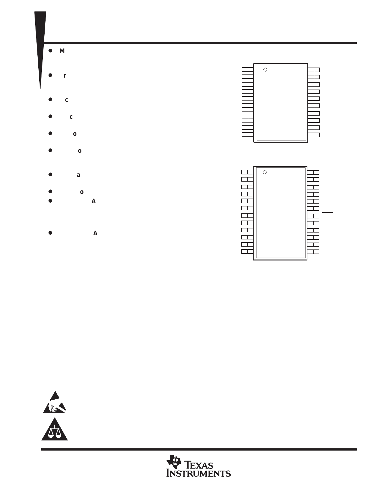
TCM37C15A ...DW OR N PACKAGE
TCM37C14A ...DW PACKAGE
(TOP VIEW)
1
2
3
4
5
6
7
8
9
10
(TOP VIEW)
1
2
3
4
5
6
7
8
9
10
11
12
20
19
18
17
16
15
14
13
12
11
24
23
22
21
20
19
18
17
16
15
14
13
V
CC
GSX
TS1
TS2
ANLGIN
AGND
PCMOUT
FSX
MCLK
DGND
V
CC
GSX
TS1
TS2
ANLGIN
AGND
TSX
PCMOUT
FSX
ASEL
MCLK
DGND
The TCM37C14A and TCM37C15A PCM combo with programmable gain control devices are single-chip PCM
combos (pulse-code-modulated CODECs with voice-band filtering). They are designed to perform transmit
encoding (A/D conversion) and receive decoding (D/A conversion), as well as the transmit and receive filtering
functions required to meet CCITT/(D3/D4) G.711 and G.714 specifications in a PCM system. Each device
provides all the functions required to interface a full-duplex, 4-line voice telephone circuit with a TDM
(time-division-multiplexed) system, and also perform the encoding and decoding of call progress tones. The
TCM37C14A and TCM37C15A are based on the proven TI TCM29C13A core, and have the added feature of
programmable transmit and receive gain.
Primary applications include line interface for digital transmission and switching of T1/E1 carrier (P ABX [private
branch automatic exchange] and central office telephone systems), subscriber line concentrators, digital
encryption systems, and digital signal processing. They are intended to be used at the analog termination of
a PCM line or trunk to the POTS (plain old telephone system) local-loop line.
The TCM37C15A is available in 20-pin DW SOIC (small-outline IC) or 20-pin N PDIP (plastic dual-in-line
package) packages, and the TCM37C14A is available in a 24-pin DW SOIC package and includes differential
output. All are characterized for operation from –40°C to 85°C.
These devices have limited built-in ESD protection. The leads should be shorted together or the device placed in conductive foam
during storage or handling to prevent electrostatic damage to the MOS gates.
Please be aware that an important notice concerning availability, standard warranty, and use in critical applications of
Texas Instruments semiconductor products and disclaimers thereto appears at the end of this data sheet.
PRODUCTION DATA information is current as of publication date.
Products conform to specifications per the terms of Texas Instruments
standard warranty. Production processing does not necessarily include
testing of all parameters.
POST OFFICE BOX 655303 • DALLAS, TEXAS 75265
Copyright 1998, Texas Instruments Incorporated
1
Page 2
TCM37C14A, TCM37C15A
T
A
PCM COMBO WITH PROGRAMMABLE GAIN CONTROL
SLWS018B – JUNE 1996 – REVISED MAY 1998
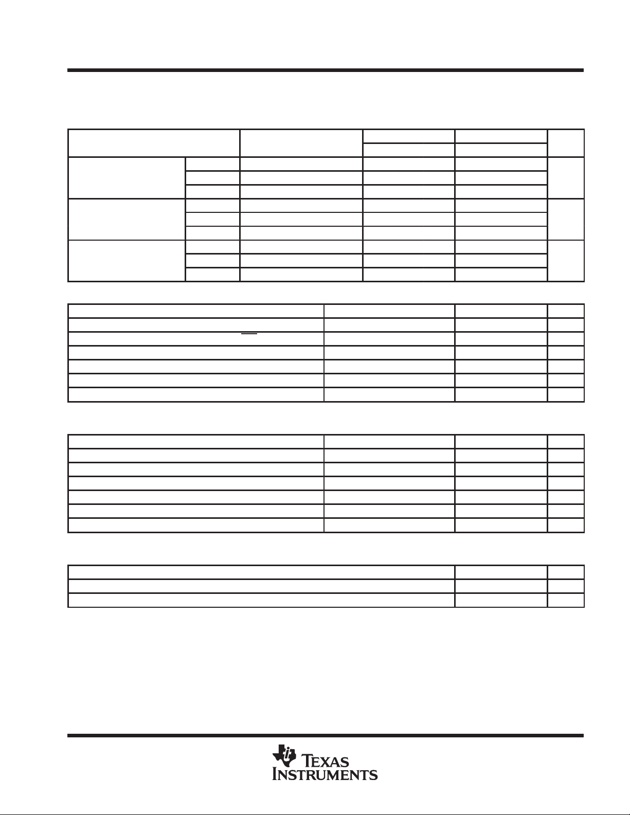
AVAILABLE OPTIONS
PACKAGE
20 PIN 24 PIN
SMALL OUTLINE
(DW)
–40°C to 85°C TCM37C15AIDW TCM37C15AIN TCM37C14AIDW
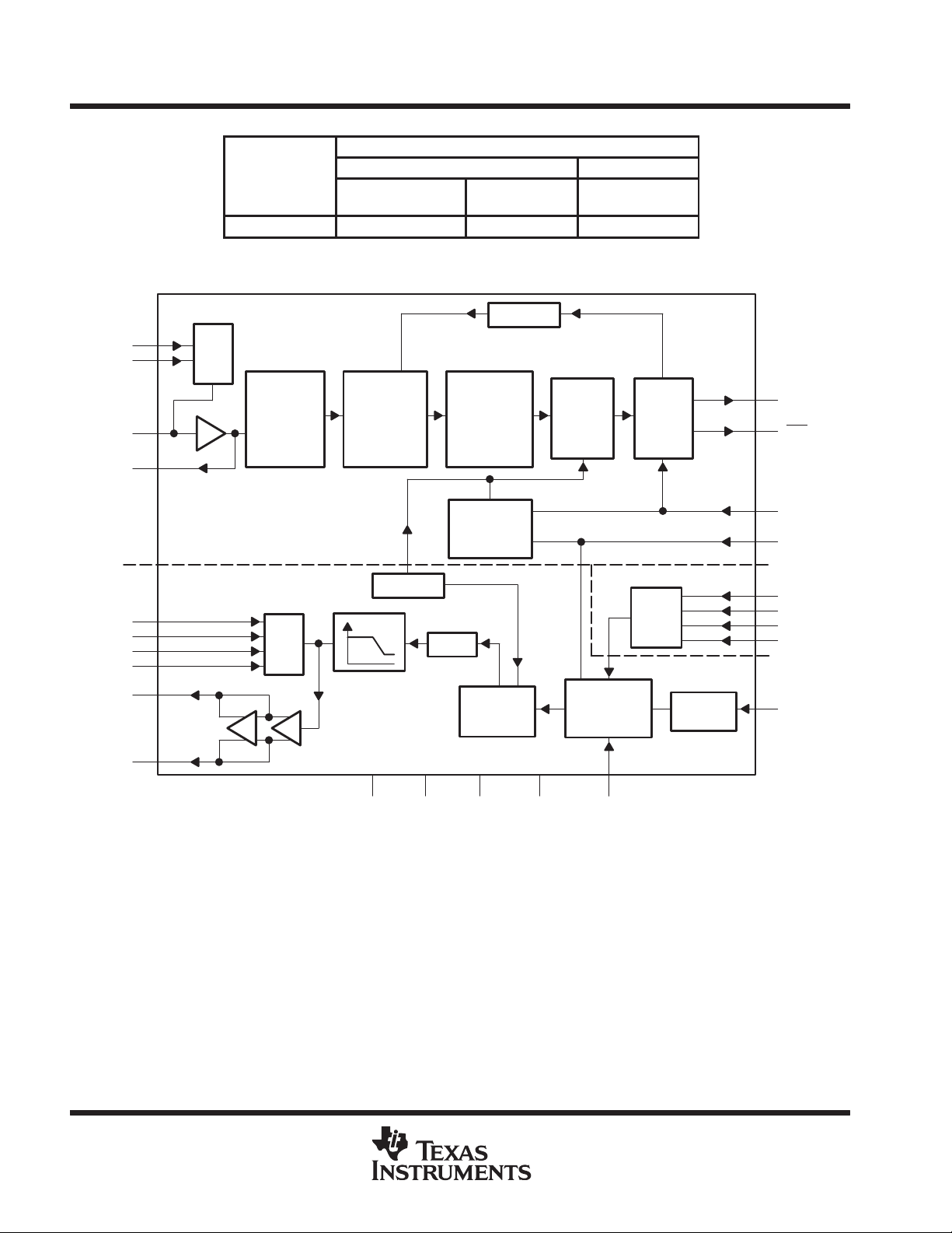
functional block diagram
PLASTIC DIP
(N)
SMALL OUTLINE
(DW)
TS1
TS2
ANLGIN
GSX
RIN
GSR
RS1
RS2
PWRO+
PWRO–
Transmit Section
22
21
20
23
4
7
5
6
2
3
†
Gain
Set
Transmit
Third-Order
Antialias
Low-Pass
Filter
(Analog)
Gain
Set
Transmit
Sixth-Order
Low-Pass
Filter
(Switched Cap)
Fc = 3400 Hz
Reference
Filter
(Switched Cap)
Buffer
Auto Zero
Transmit
Third-Order
High-Pass
Filter
Fc = 200 Hz
Analog to
Digital Control
Logic
Digital-to-
Analog
Converter
Sample
and Hold
ADC
Control SectionReceive Section
Digital-to-
Analog Control
Logic
Output
Register
Control
Logic
Input
Register
17
18
16
14
10
15
9
8
11
PCMOUT
†
TSX
FSX
MCLK
CLKSEL
†
ASEL
GS0
GS1
PCMIN
†
24 1 13 19 12
FSRAGNDDGNDVBBVCC
†
TCM37C14A only
NOTE A: Terminal numbers shown are for the TCM37C14A.
2
POST OFFICE BOX 655303 • DALLAS, TEXAS 75265
Page 3
NAME
TCM37C14A, TCM37C15A
PCM COMBO WITH PROGRAMMABLE GAIN CONTROL
SLWS018B – JUNE 1996 – REVISED MAY 1998
Terminal Functions
TERMINAL
NO.
’37C15A ’37C14A
AGND 15 19 Analog ground return for all internal voice circuits. AGND is connected internally to DGND.
ANLGIN 16 20 I Analog input to transmit operational amplifier.
ASEL 15 I Selection between A-law and µ-law operation. When ASEL is connected to VBB, A-law is selected.
CLKSEL 10 I Clock frequency selection. CLKSEL must be connected to VBB, VCC, or ground to select the master
DGND 11 13 Digital ground for all internal logic circuits. DGND is internally connected to AGND.
FSR 10 12 I Frame-synchronization clock input/time-slot enable for receive channel. The receive channel enters
FSX 13 16 I Frame-synchronization clock input/time-slot enable for transmit. The transmit channel enters the
GS0 8 9 I Input for first bit of the programmable gain control circuitry. GS0 works in combination with GS1 to
GS1 7 8 I Input for second bit of the programmable gain control circuitry . GS1 works in combination with GS0
GSR 6 7 I Input to gain-setting network of the output power amplifier. Gain is set by external resistors with three
GSX 19 23 O Output terminal of internal uncommitted operational amplifier. Internally , GSX is the voice signal input
MCLK 12 14 I Master clock (input). For the TCM37C14A, the master clock frequency can be either 2.048 MHz,
PCMIN 9 11 I Receive PCM input. PCM data is clocked in on PCMIN on eight consecutive negative transitions of
PCMOUT 14 17 O Transmit PCM output. PCM data is clocked out on PCMOUT on eight consecutive positive transitions
PWRO+ 2 2 O Noninverting output of power amplifier. PWRO+ can drive transformer hybrids or high-impedance
PWRO– 3 O Inverting output of power amplifier. PWRO– is functionally identical with and complementary to
RIN 3 4 I Input to receive section amplifiers. (See Figure 6 and Figure 7 for recommended circuitry.)
RS1 4 5 Terminal for first gain-control resistor of the receive section. RS1 is selected through closure of the
RS2 5 6 Terminal for second gain control resistor of the receive section. RS2 is selected through closure of
TS1 18 22 Terminal for gain-control resistor on input of transmit section. TS1 is selected through closure of the
TS2 17 21 Terminal for gain-control resistor on input of transmit section. TS2 is selected through closure of the
TSX 18 O Transmit channel time-slot strobe for the transmit channel (active low). TSX is an open drain output
V
BB
V
CC
1 1 Negative supply voltage. Input is –5 V ± 5%.
20 24 Positive supply voltage. Input is 5 V ± 5%.
I/O DESCRIPTION
When ASEL is connected to VCC or ground, µ-law is selected.
clock frequency. When CLKSEL is tied to VBB, MCLK is 2.048 MHz. When it is tied to ground, MCLK
is at 1.544 MHz. When it is tied to VCC, MCLK is 1.536 MHz.
the standby state when FSR is held low for 300 ms.
standby state when FSX is held low for 300 ms.
simultaneously control transmit and receive gain, and controls power-down instruction. (See
Table 1 and 2 for control logic information.)
to simultaneously control transmit and receive gain, and controls power-down instruction. (See T able
1 and 2 for control logic information.)
levels of programmable gain or attenuation control. (See Figure 6 and Figure 7 for recommended
configuration.)
to the transmit filter.
1.544 MHz, or 1.536 MHz, and is selected by CLKSEL. MCLK for the TCM37C15A is 2.048 MHz.
the receive data clock (MCLK).
of the transmit data clock (MCLK).
loads directly in a differential or a single-ended configuration.
PWRO +.
first gain control switch. (See Figure 6 and Figure 7 for recommended circuitry.)
the second gain control switch. (See Figure 6 and Figure 7 for recommended configuration.)
first gain-control switch. (See Figure 6 and Figure 7 for recommended configuration.)
second gain-control switch. (See Figure 6 and Figure 7 for recommended configuration.)
and can be used as an enable signal for a 3-state output buffer .
POST OFFICE BOX 655303 • DALLAS, TEXAS 75265
3
Page 4
TCM37C14A, TCM37C15A
Load resistance, R
Load capacitance, C
pF
PCM COMBO WITH PROGRAMMABLE GAIN CONTROL
SLWS018B – JUNE 1996 – REVISED MAY 1998
absolute maximum ratings over operating free-air temperature range (unless otherwise noted)
Supply voltage, V
Supply voltage, V
Voltage range at any analog input, V
(see Note 1) 7 V. . . . . . . . . . . . . . . . . . . . . . . . . . . . . . . . . . . . . . . . . . . . . . . . . . . . . . . . . . . . .
CC
(see Note 1) –7 V. . . . . . . . . . . . . . . . . . . . . . . . . . . . . . . . . . . . . . . . . . . . . . . . . . . . . . . . . . . .
BB
V
I
+ 0.3 V to V
CC
BB
†
– 0.3 V. . . . . . . . . . . . . . . . . . . . . . . . . . . . . . . . . . . . .
Continuous total power dissipation at (or below) 25°C free-air temperature 1300 mW. . . . . . . . . . . . . . . . . . .
Operating free-air temperature range, T
Storage temperature range, T
–65°C to 150°C. . . . . . . . . . . . . . . . . . . . . . . . . . . . . . . . . . . . . . . . . . . . . . . . . . .
stg
–40°C to 85°C. . . . . . . . . . . . . . . . . . . . . . . . . . . . . . . . . . . . . . . . . . . .
A
Lead temperature 1,6 mm (1/16 inch) from case for 10 seconds: DW or N package 260°C. . . . . . . . . . . . . . .
JEDEC Latch up ±250 mA or ±10 V. . . . . . . . . . . . . . . . . . . . . . . . . . . . . . . . . . . . . . . . . . . . . . . . . . . . . . . . . . . . . .
†
Stresses beyond those listed under “absolute maximum ratings” may cause permanent damage to the device. These are stress ratings only, and
functional operation of the device at these or any other conditions beyond those indicated under “recommended operating conditions” is not
implied. Exposure to absolute-maximum-rated conditions for extended periods may affect device reliability.
NOTE 1: Voltage values are with respect to GND.
recommended operating conditions (see Note 2)
MIN NOM MAX UNIT
Supply voltage, VCC (see Notes 2 and 3) 4.75 5 5.25 V
Supply voltage, V
DGND voltage with respect to AGND 0 V
High-level input voltage, V
Low-level input voltage, V
p
Operating free-air temperature, T
NOTES: 2. To avoid possible damage to these CMOS devices and resulting reliability problems, the power-up procedure described in the device
BB
IH
IL
L
L
A
power-up sequence paragraphs later in this document should be followed.
3. Voltages at analog inputs and outputs, VCC and VBB terminals, are with respect to the AGND terminal. All other voltages are
referenced to the DGND terminal unless otherwise noted.
At GSX/GSR 10 kΩ
At PWRO+ and/or PWRO– 300 Ω
At GSX/GSR 50
At PWRO+ and/or PWRO– 100
–4.75 –5 –5.25 V
2.2 V
0.8 V
p
–40 85 °C
4
POST OFFICE BOX 655303 • DALLAS, TEXAS 75265
Page 5
PARAMETER
TEST CONDITIONS
UNIT
V
CC
V
BB
TCM37C14A, TCM37C15A
PCM COMBO WITH PROGRAMMABLE GAIN CONTROL
SLWS018B – JUNE 1996 – REVISED MAY 1998
electrical characteristics over recommended ranges of supply voltage and operating free-air
temperature (outputs not loaded) (unless otherwise noted)
supply current
0°C to 85°C –40°C to 0°C
MIN TYP MAX MIN TYP MAX
Supply current from
I
CC
Supply current from
I
BB
PDPower dissipation
digital interface
V
High-level output voltage at PCMOUT IOH = –9.6 mA 2.4 V
OH
V
Low-level output voltage at PCMOUT, TSX IOL = 3.2 mA 0.5 V
OL
I
High-level input current, any digital input VI = 2.2 V to V
IH
I
Low-level input current, any digital input VI = 0 to 0.8 V 12 µA
IL
C
Input capacitance 5 pF
i
C
Output capacitance 5 pF
o
†
All typical values are at VBB = –5 V , VCC = 5 V, and TA = 25°C.
Operating 7 10 8 11
Standby FSX, FSR at VIL (after 300 ms) 0.5 1.3 1 1.7
Power down GS0, GS1 = VIL (after 300 ms) 0.5 1.2 1 1.7
Operating –7 –9 –9 –11.5
Standby FSX, FSR at VIL (after 300 ms) –0.6 –1 –0.8 –1.2
Power down GS0, GS1 = VIL (after 300 ms) –0.3 –0.9 –0.4 –1.2
Operating 70 100 80 110
Standby
Power down GS0, GS1 = VIL (after 300 ms) 7 12 10 17
PARAMETER TEST CONDITIONS MIN TYP†MAX UNIT
FSX, FSR at VIL (after 300 ms) 9 13 10 17
CC
mA
mA
mW
12 µA
transmit amplifier input
PARAMETER TEST CONDITIONS MIN TYP†MAX UNIT
Input current at ANLGIN VI = –2.17 V to 2.17 V ±100 nA
Input offset voltage at ANLGIN VI = –2.17 V to 2.17 V ±25 mV
Common-mode rejection at ANLGIN VI = –2.17 V to 2.17 V 55 dB
Open-loop voltage amplification at GSX 5000
Open-loop unity-gain bandwidth at GSX 1 MHz
Input resistance at ANLGIN 10 MΩ
†
All typical values are at VBB = –5 V , VCC = 5 V, and TA = 25°C.
receive filter output‡
PARAMETER MIN TYP†MAX UNIT
Output offset voltage PWRO+, PWRO– (single ended), Relative to AGND 80 mV
Output resistance at PWRO+, PWRO– 1 Ω
†
All typical values are at VBB = –5 V , VCC = 5 V, and TA = 25°C.
‡
PWRO– on TCM37C14A only
POST OFFICE BOX 655303 • DALLAS, TEXAS 75265
5
Page 6
TCM37C14A, TCM37C15A
R
600 Ω
Zero-transmission-level point, transmit channel (0 dBm0)
dBm
R
900 Ω
R
600 Ω
Zero-transmission-level point, receive channel (0 dBm0)
dBm
R
900 Ω
PCM COMBO WITH PROGRAMMABLE GAIN CONTROL
SLWS018B – JUNE 1996 – REVISED MAY 1998
electrical characteristics over recommended ranges of supply voltage and operating free-air
temperature (outputs not loaded) (unless otherwise noted) (continued)
gain and dynamic range, V
PARAMETER TEST CONDITIONS MIN TYP MAX UNIT
Encoder milliwatt response (transmit gain tolerance)
Encoder milliwatt response variation with temperature and
supplies
Digital milliwatt response (receive gain tolerance) relative to zero-
transmission level point
Digital milliwatt response variation with temperature and supplies TA = –40°C – 85°C, supplies = ±5% ±0.08 dB
p
p
NOTES: 4. Unless otherwise noted, the analog input is a 0-dBm0, 1020-Hz sine wave, where 0 dBm0 is defined as the zero-reference point
of the channel under test with unity gain set on the amplifier. This corresponds to an analog signal input of 1.064 V rms, or an output
of 1.503 Vrms.
5. The input amplifier is set for unity gain, noninverting. The digital input is a PCM bit stream generated by passing a 0-dBm0, 1020-Hz
sine wave through an ideal encoder.
6. Receive output is measured single ended with the output amplifier in the unity-gain configuration. All output levels are (sin x)/x
corrected.
= 5 V, VBB = –5 V, TA = 25°C (see Notes 4, 5, and 6) (unless otherwise noted)
CC
µ-law
A-law
µ-law
A-law
µ-law
A-law
µ-law
A-law
Signal input = 1.064 Vrms for µ-law,
Signal input = 1.068 Vrms for A-law
TA = –40°C – 85°C, supplies = ±5% ±0.08 dB
Signal input per CCITT G.711,
output signal = 1 kHz
=
L
=
L
=
L
=
L
±0.04 ±0.2 dBm0
±0.04 ±0.2 dBm0
2.76
2.79
1
1.03
5.76
5.79
4
4.03
gain tracking, reference level = –10 dBm0
PARAMETER TEST CONDITIONS MIN MAX UNIT
3 > input level ≥ –40 dBm0 ±0.25
Transmit gain tracking error , sinusoidal input
Receive gain tracking error, sinusoidal input
–40 > input level ≥ –50dBm0 ±0.5
–50 > input level ≥ –55 dBm0 ±1.2
3 > input level ≥ –40 dBm0 ±0.25
–40 > input level ≥ –50 dBm0 ±0.5
–50 > input level ≥ –55 dBm0 ±1.2
dB
dB
noise
PARAMETER TEST CONDITIONS MIN TYP†MAX UNIT
Transmit noise, C-message weighted ANLGIN = AGND 1 7 dBrnC0
Transmit noise, psophometrically weighted ANLGIN = AGND –82 –80 dBm0p
Receive noise, C-message-weighted quiet code at PWRO+
Receive noise, psophometrically weighted PCM = lowest positive decode level –81 dBm0p
†
All typical values are at VBB = –5 V , VCC = 5 V, and TA = 25°C.
PCMIN = 11111111 (µ-law),
PCMIN = 11010101 (A-law)
2 5 dBrnC0
6
POST OFFICE BOX 655303 • DALLAS, TEXAS 75265
Page 7
V
ppl
oltage rejection ratio, transmit channel
200 mV
dB
y
V
ppl
oltage rejection ratio, transmit channel
yg ,
dB
y
CC
ygj ,
yg ,
dB
y
BB
ygj ,
yg ,
dB
dBm0
TCM37C14A, TCM37C15A
PCM COMBO WITH PROGRAMMABLE GAIN CONTROL
SLWS018B – JUNE 1996 – REVISED MAY 1998
electrical characteristics over recommended ranges of supply voltage and operating free-air
temperature (outputs not loaded) (unless otherwise noted) (continued)
power supply rejection and crosstalk attenuation
PARAMETER TEST CONDITIONS MIN TYP†MAX UNIT
pp
su
CC
BB
V
(single ended)
V
(single ended)
Crosstalk attenuation, transmit-to-receive at PWRO+ (single ended)
Crosstalk attenuation, receive-to-transmit at PWRO+ (single ended)
†
All typical values are at VBB = –5 V , VCC = 5 V, and TA = 25°C.
y v
pp
su
y v
supply voltage rejection ratio, receive channel
supply voltage rejection ratio, receive channel
0 < f < 30 kHz
30 < f < 50 kHz
0 < f < 30 kHz
30 < f < 50 kHz
0 < f < 30 kHz
30 < f < 50 kHz
0 < f < 30 kHz
30 < f < 50 kHz
Idle channel,
pp
supply signal =
f measured at PCMOUT
Idle channel,
suppl
signal = 200 mVpp,
f measured at PCMOUT
Idle channel,
Idle channel,
suppl
signal = 200 mVpp,
narrow-band,
f measured at PWRO+
Idle channel,
suppl
signal = 200 mVpp,
narrow-band,
f measured at PWRO+
ANLGIN = 0 dBm0,
f = 1.02 kHz, unity gain,
PCMIN = lowest decode level
PCMIN = 0 dBm0,
f = 1.02 kHz
pp
pp,
–40
–45
–35
–55
–40
–45
–40
–45
75 dB
75 dB
distortion
PARAMETER TEST CONDITIONS MIN MAX UNIT
0 > ANLGIN ≥ –30 dBm0 36
Transmit signal to distortion ratio, sinusoidal input (CCITT G.712 – Method 2)
Receive signal to distortion ratio, sinusoidal input (CCITT G.712 – Method 2)
Transmit single-frequency distortion products Input signal = 0 dBm0 –46 dBm0
Receive single-frequency distortion products Input signal = 0 dBm0 –46 dBm0
Intermodulation distortion, end-to-end
Spurious out-of-band signals, end-to-end
–30 > ANLGIN ≥ –40 dBm0 30
–40 > ANLGIN ≥ –45 dBm0 25
0 > ANLGIN ≥ –30 dBm0 36
–30 > ANLGIN ≥ –40 dBm0 30
–40 > ANLGIN ≥ –45 dBm0 25
CCITT G.712 (7.1) –35
CCITT G.712 (7.2) –49
CCITT G.712 (6.1) –25
CCITT G.712 (9) –40
dB
dB
POST OFFICE BOX 655303 • DALLAS, TEXAS 75265
7
Page 8

TCM37C14A, TCM37C15A
y
s
y
s
(g ) g
Noninverting maximum gain out ut
g
dB
In ut signal at ANLGIN is 0 dBm0
Gain (voltage amplification) relative to gain at 1.02 kH
Input signal at PCMIN is 0 dBm0
dB
PCM COMBO WITH PROGRAMMABLE GAIN CONTROL
SLWS018B – JUNE 1996 – REVISED MAY 1998
electrical characteristics over recommended ranges of supply voltage and operating free-air
temperature (outputs not loaded) (unless otherwise noted) (continued)
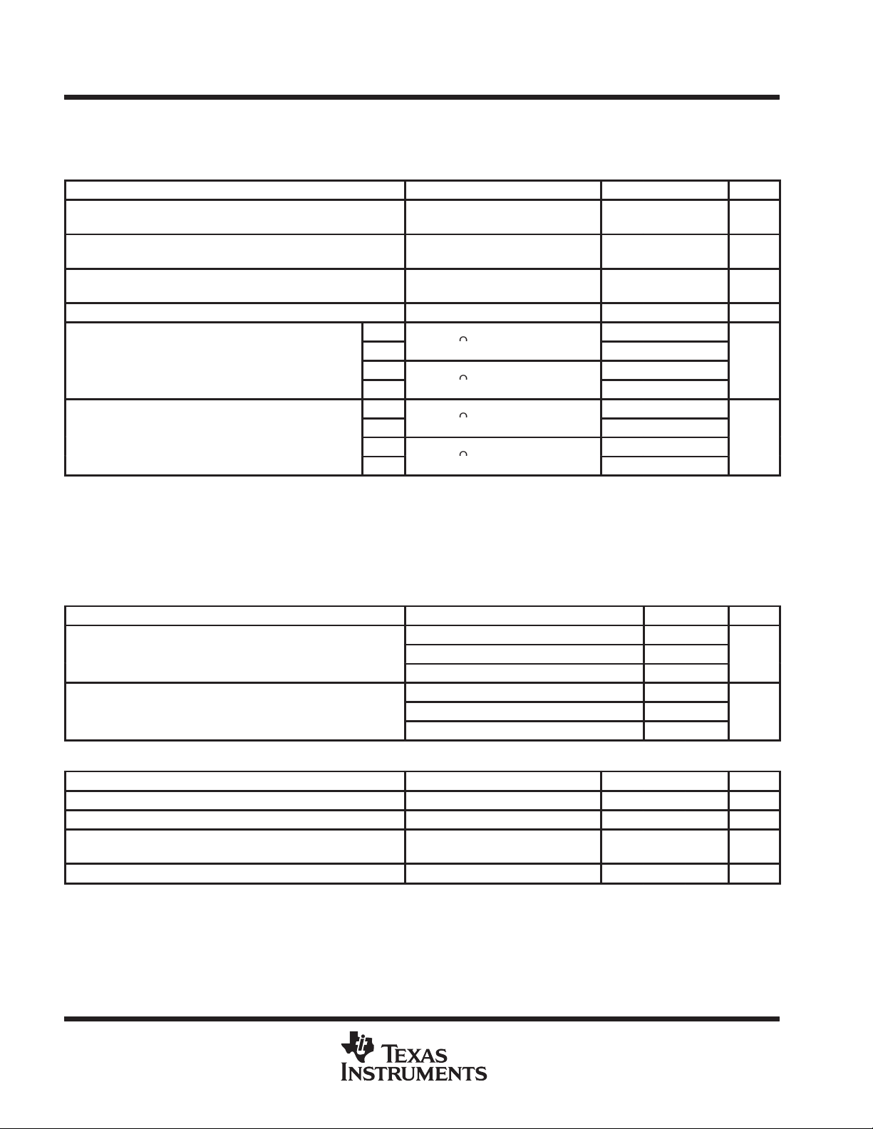
transmit filter transfer function (see Figure 1)
PARAMETER TEST CONDITIONS MIN TYP
f
= 2.048 MHz,
Transmit absolute delay time to PCMOUT
Transmit differential envelope delay time
relative to transmit absolute delay time
Receive absolute delay time to PWRO+ f
Receive differential envelope delay time
relative to transmit absolute delay time
Gain (voltage amplification) relative to gain
at 1.02 kHz
†
All typical values are at VBB = –5 V , VCC = 5 V, and TA = 25°C.
MCLK
Input to ANLGIN is 1.02 kHz at 0 dBm0
f = 500 Hz to 600 Hz 170
f = 600 Hz to 1000 Hz 95
f = 1000 Hz to 2600 Hz 45
f = 2600 Hz to 2800 Hz 105
= 2.048 MHz, Digital input is digital milliwatt codes 190 µs
MCLK
f = 500 Hz to 600 Hz 45
f = 600 Hz to 1000 Hz 35
f = 1000 Hz to 2600 Hz 85
f = 2600 Hz to 2800 Hz 110
Input amplifier set for unity gain,
Input si
nal at ANLGIN is 0 dBm0
16.67 Hz –30
50 Hz –25
60 Hz –23
200 Hz –1.8 –0.125
,
p
300 Hz to 3 kHz –0.15 0.15
3.3 kHz –0.35 0.15
3.4 kHz –1 –0.1
4 kHz –14
†
MAX UNIT
245 µs
µ
µ
receive filter transfer function (see Figure 2)
PARAMETER TEST CONDITIONS MIN MAX UNIT
Below 20 Hz 0.15
20 Hz 0.15
200 Hz –0.5 0.15
p
p
z
300 Hz to 3 kHz –0.15 0.15
3.3 kHz –0.35 0.15
3.4 kHz –1 –0.1
4 kHz –14
4.6 kHz and above –30
timing requirements over recommended ranges of supply voltage and operating free-air
temperature (unless otherwise noted)
clock timing (see Figure 3)
MIN NOM MAX UNIT
t
c(MCLK)
t
r
t
f
t
w(MCLK)
NOTE 7: FSX CLK and FSR CLK must be phase-locked with MCLK.
Clock period, MCLK (2.048 MHz systems) 488 ns
Rise time, MCLK 5 30 ns
Fall time, MCLK 5 30 ns
Pulse duration, MCLK (see Note 7) 220 ns
Clock duty cycle [t
w(CLK)/tc(CLK)
], MCLK 45% 50% 55%
8
POST OFFICE BOX 655303 • DALLAS, TEXAS 75265
Page 9

TCM37C14A, TCM37C15A
PCM COMBO WITH PROGRAMMABLE GAIN CONTROL
SLWS018B – JUNE 1996 – REVISED MAY 1998
timing requirements over recommended ranges of supply voltage and operating free-air
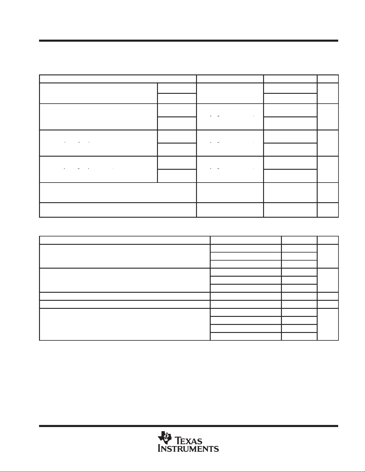
temperature (unless otherwise noted) (continued)
transmit timing (see Figure 3)
MIN MAX UNIT
t
d(FSX)
receive timing (see Figure 4)
t
d(FSR)
t
su(PCMIN)
t
h(PCMIN)
switching characteristics over recommended ranges of operating conditions
(see Figures 3 and 4)
t
pd1
t
pd2
t
pd3
t
pd4
t
pd5
NOTE 8: Timing parameters t
Delay time (frame sync), FSX high or low before MCLK ↓ 100 t
Delay time (frame sync), FSR high or low before MCLK ↓ 100 t
Setup time, PCMIN high before MCLK ↓ 50 ns
Hold time after PCMIN ↓ 60 ns
PARAMETER TEST CONDITIONS MIN MAX UNIT
Propagation delay time, MCLK ↑ to bit 1 data valid at PCMOUT (data enable time
on time slot entry) (see Note 8)
Propagation delay time, MCLK ↑ bit n to bit n data valid at PCMOUT (data valid
time)
Propagation delay time, MCLK ↓ low bit 8 to bit 8 Hi-Z at PCMOUT (data float
time on time slot exit) (see Note 8)
Propagation delay time, MCLK ↑ bit 1 to TSX active (low) (time slot enable time) CL = 0 pF to 100 pF 0 145 ns
Propagation delay time, MCLK ↓ to bit 8 to TSX inactive (high) (timeslot disable
time) (see Note 8)
, t
pd1
pd3
, and t
are referenced to the high-impedance state.
pd5
CL = 0 pF to 100 pF 0 145 ns
CL = 0 pF to 100 pF 0 145 ns
CL = 0 pF 60 215 ns
CL = 0 pF 60 190 ns
c(MCLK)
MIN MAX UNIT
c(MCLK)
–100 ns
–100 ns
POST OFFICE BOX 655303 • DALLAS, TEXAS 75265
9
Page 10

TCM37C14A, TCM37C15A
PCM COMBO WITH PROGRAMMABLE GAIN CONTROL
SLWS018B – JUNE 1996 – REVISED MAY 1998
PARAMETER MEASUREMENT INFORMATION
0
–1
0
–10
–20
– Gain Relative to Gain at 1 kHz – dB
V
A
–30
–30 dB
16.67 Hz
–23 dB
60 Hz
–25 dB
50 Hz
–0.125 dB
200 Hz
–1.8 dB
200 Hz
0.15 dB
300 Hz
–0.15 dB
300 Hz
Typical Filter
Transfer Function
Typical Filter
Transfer Function
0.15 dB
3000 Hz
–0.15 dB
3000 Hz
–0.35 dB
3300 Hz
–1dB
3400 Hz
0.15 dB
3300 Hz
–0.10 dB
3400 Hz
–14 dB
4000 Hz
–32 dB
4600 Hz
0
Expanded Scale
–1
0
–10
–20
–30
–40
–60 –60
f – Frequency – Hz
NOTE A: Gain (voltage amplification) is defined as gain relative to gain at 1 kHz in dB.
–40
–50–50
10 k1 k1005010
Figure 1. Transmit Filter Transfer Characteristics
10
POST OFFICE BOX 655303 • DALLAS, TEXAS 75265
Page 11

TCM37C14A, TCM37C15A
PCM COMBO WITH PROGRAMMABLE GAIN CONTROL
SLWS018B – JUNE 1996 – REVISED MAY 1998
PARAMETER MEASUREMENT INFORMATION
0.15 dB
3000 HZ
–0.15 dB
3000 Hz
–1dB
3400 Hz
0.15 dB
3300 HZ
–0.10 dB
3400 Hz
0
–1
Expanded Scale
–1
0.15 dB
200 Hz
0
–0.15 dB
200 Hz
0.15 dB
300 Hz
–0.15 dB
300 Hz
–0.35 dB
3300 Hz
0
–10
–14 dB
4000 Hz
–20
–30 dB
– Gain Relative to Gain at 1 kHz – dBA
–30
V
–40
Typical Filter
Transfer Function
4800 Hz
0
–10
–20
–30
–40
–50–50
50 100
NOTE A: Gain (voltage amplification) is defined as gain relative to gain at 1 kHz in dB.
1 k
f – Frequency – Hz
Figure 2. Receive Filter Transfer Characteristics
POST OFFICE BOX 655303 • DALLAS, TEXAS 75265
–60–60
10 k
11
Page 12

TCM37C14A, TCM37C15A
PCM COMBO WITH PROGRAMMABLE GAIN CONTROL
SLWS018B – JUNE 1996 – REVISED MAY 1998
PARAMETER MEASUREMENT INFORMATION
Time Slot 1
MCLK
t
d(FSX)
FSX
t
pd1
PCMOUT
TSX
†
Bit 1 = MSB = most significant bit (sign bit) and is clocked in first on PCMIN or clocked out first on PCMOUT.
‡
Bit 8 = LSB = least significant bit and is clocked in last on PCMIN or is clocked out last on PCMOUT.
NOTE A: Inputs are driven from 0.45 V to 2.4 V . T ime intervals are referenced to 2 V when the high level is indicated and 0.8 V when the low
level is indicated.
12345678
Bit 1
t
d(FSX)
†
t
pd4
t
r
t
pd2
Bit 2 Bit 3 Bit 4 Bit 5 Bit 6 Bit 7 Bit 8
t
f
t
w(MCLK)
t
c(MCLK)
t
pd5
t
pd3
‡
Figure 3. Transmit Timing
Time Slot 1
MCLK
t
d(FSR)
FSR
12345678
t
d(FSR)
t
r
t
f
t
w(MCLK)
t
c(MCLK)
t
su(PCMIN)
t
h(PCMIN)
PCMIN
†
Bit 1
Valid
†
Bit 1 = MSB = most significant bit (sign bit) and is clocked in first on PCMIN or clocked out first on PCMOUT.
‡
Bit 8 = LSB = least significant bit and is clocked in last on PCMIN or is clocked out last on PCMOUT.
NOTE A: Inputs are driven from 0.45 V to 2.4 V . T ime intervals are referenced to 2 V when the high level is indicated and 0.8 V when the low
level is indicated.
Bit 2
Valid
Bit 3
Valid
Bit 4
Valid
Bit 5
Valid
Bit 6
Valid
Bit 7
Valid
Bit 8
Valid
‡
Figure 4. Receive Timing
12
POST OFFICE BOX 655303 • DALLAS, TEXAS 75265
Page 13

TCM37C14A, TCM37C15A
PCM COMBO WITH PROGRAMMABLE GAIN CONTROL
SLWS018B – JUNE 1996 – REVISED MAY 1998
PRINCIPLES OF OPERATION
system reliability and design considerations
The TCM37C14A and TCM37C15A system reliability and design considerations are described in the following
paragraphs.
latch-up
Latch-up is possible in all CMOS devices. It is caused by the firing of a parasitic SCR that is present due to the
inherent nature of CMOS. When a latch-up occurs, the device draws excessive amounts of current and will
continue to draw heavy current until power is removed. Latch-up can result in permanent damage to the device
if supply current to the device is not limited.
Even though the devices are heavily protected against latch-up, it is still possible to cause latch-up under certain
conditions in which excess current is forced into or out of one or more terminals. Latch-up can occur when the
positive supply voltage drops momentarily below ground, when the negative supply voltage rises momentarily
above ground, or, possibly , if a signal is applied to a terminal after power has been applied but before the ground
is connected. This can happen if the device is hot inserted into a card with the power applied, or if the device
is mounted on a card that has an edge connector, and the card is hot inserted into a system with the power on.
To help ensure that latch-up does not occur, it is considered good design practice to connect a reverse-biased
Schottky diode with a forward voltage drop of less than or equal to 0.4 V (1N571 1 or equivalent) between each
power supply and GND (see Figure 5). If it is possible that a TCM37C14A- or TCM37C15A-equipped card with
an edge connector could be hot inserted into a powered-up system, it is also important to ensure that the ground
edge-connector traces are longer than the power and signal traces, so that the card ground is always the first
to make contact.
V
CC
DGND
V
BB
Figure 5. Latch-Up Protection Diode Connection
POST OFFICE BOX 655303 • DALLAS, TEXAS 75265
13
Page 14

TCM37C14A, TCM37C15A
PCM COMBO WITH PROGRAMMABLE GAIN CONTROL
SLWS018B – JUNE 1996 – REVISED MAY 1998
PRINCIPLES OF OPERATION
system reliability and design considerations (continued)
device power-up sequence
Latch-up also can occur if a signal source is connected without the device being properly grounded. A signal
applied to one terminal could then find a ground through another signal terminal on the device. T o ensure proper
operation of the device and as a safeguard against this sort of latch-up, it is recommended that the following
power-up sequence always be used:
1. Ensure that no signals are applied to the device before the power-up sequence is complete.
2. Connect GND.
3. Apply V
4. Apply V
(most negative voltage).
BB
(most positive voltage).
CC
5. Force a power down condition in the device.
6. Connect the master clock.
7. Release the power-down condition.
8. Apply FSX and/or FSR synchronization pulses.
9. Apply signal inputs.
When powering down the device, this procedure should be followed in the reverse order.
internal sequencing
On the transmit channel, digital outputs PCMOUT and TSX
approximately four frames (500 µs) after power up or application of V
†
TSX
are functional and occur in the proper timeslot. The analog circuits on the transmit side require
†
are held in the high-impedance state for
or VCC. After this delay , PCMOUT and
BB
approximately 60 ms to reach their equilibrium value due to the autozero circuit settling time. Thus, valid digital
information, such as for on/off hook detection, is available almost immediately, while analog information is
available after some delay.
To further enhance system reliability , the PCMOUT and TSX
†
terminals are placed in a high-impedance state
approximately 20 µs after an interruption of MCLK. This interruption could possibly occur with some kind of fault
condition elsewhere in the system.
†
TCM37C14A only
miscellaneous functions
Miscellaneous functions of the TCM37C14A and TCM37C15A are described in the following paragraphs.
gain/attenuation control
On-chip logic is included on the TCM37C14A and TCM37C15A to control the channel gain or attenuation and
power-down functions with minimum terminal allocation. The operational amplifiers in the receive and transmit
sections can be configured to either attenuate or amplify the signal depending on how external resistors are
connected to the device.
Two control input terminals (GS0 and GS1) select one of three levels of gain or attenuation in the transmit and
receive path as well as power-down. Note that the gain for both the transmit and receive sides are set together
and that the device enters the power-down mode when both GS0 and GS1 are held low.
14
POST OFFICE BOX 655303 • DALLAS, TEXAS 75265
Page 15

TCM37C14A, TCM37C15A
PCM COMBO WITH PROGRAMMABLE GAIN CONTROL
SLWS018B – JUNE 1996 – REVISED MAY 1998
PRINCIPLES OF OPERATION
miscellaneous functions (continued)
gain adjustment
If gain is used on the receive side, the input PCM data levels must be properly limited to prevent saturation of
the output amplifier. Refer to the gain and dynamic range table in the electrical characteristics section.
The gain of the transmit and receive amplifiers is set by external resistors connected to the device as shown
in Figure 6 and can be adjusted using internal switching elements as shown in Table 1.
RSIN
RSA
RSB
PWRO+
RIN
RS1
RS2
GSR
Analog Input
Analog Output
Receive Gain Control Circuitry
(Gain Configuration)
RSF
S0
S1
AGND
From Buffer
RTIN
RTA
RTB
Transmit Gain Control Circuitry
(Gain Configuration)
_
+
GSX
RTF
ANLGIN
TS1
TS2
_
+
S0
S1
AGND
Figure 6. Gain Control Circuitry
Table 1. Logic Table for Programmable Gain Control
CONTROL
TERMINALS
GS0 GS1 RS1 RS2 TS1 TS2 RECEIVE TRANSMIT
Low Low Power Down
Low Hi Open Open Open Open – RSF/RSIN – RTF/RTIN
Hi Low Closed Open Closed Open – RSF/RSIN || RSA – RTF/RTIN || RTA
Hi Hi Open Closed Open Closed – RSF/RSIN || RSB – RTF/RTIN || RTB
INTERNAL SWITCH POSITION
POST OFFICE BOX 655303 • DALLAS, TEXAS 75265
TRANSFER FUNCTION
(GAIN)
15
Page 16

TCM37C14A, TCM37C15A
PCM COMBO WITH PROGRAMMABLE GAIN CONTROL
SLWS018B – JUNE 1996 – REVISED MAY 1998
PRINCIPLES OF OPERATION
miscellaneous functions (continued)
attenuation adjust
The attenuation of the transmit and receive amplifiers is set by external resistors connected to the device as
shown in Figure 7 and can be adjusted using internal switching elements as shown in Table 2.
Analog Output
RSF
RSIN
Receive Gain Control Circuitry
(Attenuation Configuration)
RSB
RSA
Analog Input
PWRO+
S0
RS1
RS2
RIN
GSR
S1
From Buffer
RTA
RTF
RTIN
Transmit Gain Control Circuitry
(Attenuation Configuration)
_
+
AGND
GSX
RTB
TS1
TS2
ANLGIN
S0
S1
_
+
AGND
16
Figure 7. Attenuation Control Circuitry
Table 2. Logic Table for Programmable Attenuation Control
CONTROL
TERMINALS
GS0 GS1 RS1 RS2 TS1 TS2 RECEIVE TRANSMIT
Low Low Power Down
Low Hi Open Open Open Open – RSF/RSIN – RTF/RTIN
Hi Low Closed Open Closed Open – RSF || RSB/RSIN – RTF || RTB/RTIN
Hi Hi Open Closed OPEN Closed – RSF || RSA/RSIN – RTF || RTA/RTIN
INTERNAL SWITCH POSITION
POST OFFICE BOX 655303 • DALLAS, TEXAS 75265
TRANSFER FUNCTION
(ATTENUATION)
Page 17

TCM37C14A, TCM37C15A
PCM COMBO WITH PROGRAMMABLE GAIN CONTROL
SLWS018B – JUNE 1996 – REVISED MAY 1998
PRINCIPLES OF OPERATION
miscellaneous functions (continued)
power-down and standby operations
T o minimize power consumption, a power-down mode and three standby modes are provided. For power down,
low signals are applied to terminals GS0 and GS1. In the power-down mode, the average power consumption
is reduced to approximately 7 mW.
The three standby modes give the options of placing the entire device on standby, placing only the transmit
channel on standby , or placing only the receive channel on standby . T o place the entire device on standby , both
FSX and FSR are held low. For transmit-only operation, FSX is high and FSR is held low. For receive-only
operation, FSR is high and FSX is low (see Table 3 for power-down and standby procedures).
Table 3. Power-Down and Standby Procedures
DEVICE STATUS PROCEDURE
Power down GS0 and GS1 are low. 7 mW TSX and PCMOUT are in the high-impedance state.
Entire device on standby FSX and FSR are low. 9 mW TSX and PCMOUT are in the high-impedance state.
Only transmit on standby FSX is low, FSR is high. 50 mW
Only receive on standby FSR is low, FSX is high. 30 mW
TYPICAL POWER
CONSUMPTION
DIGITAL OUTPUT STATUS
TSX and PCMOUT are placed in the high-impedance state
within 300 ms.
fixed-data-rate timing
Fixed-data-rate timing uses master clock MCLK, frame synchronizer clocks FSX and FSR, and output TSX
(TCM37C14A only). An 8-kHz clock signal should be applied to the FSX and FSR inputs to set the sampling
frequency. Data is transmitted on PCMOUT on the first eight positive transitions of MCLK following the rising
edge of FSX. Data is received on PCMIN on the first eight falling edges of MCLK following FSR. A D/A
conversion is performed on the received digital word and the resulting analog sample voltage is held on an
internal sample-and-hold capacitor until transferred to the receive filter.
The TCM37C14A operates with MCLK frequencies of 1.536 MHz, 1.544 MHz, or 2.048 MHz, while the
TCM37C15A operates at 2.048 MHz.
precision voltage references
Voltage references that determine the gain and dynamic range characteristics of the device are generated
internally and require no external components to operate. A difference in subsurface charge density between
two suitably implanted MOS devices is used to derive a temperature- and bias-stable reference voltage. These
references are calibrated during the manufacturing process. Separate references are supplied to the transmit
and receive sections, and each is calibrated independently . Each reference value is then further trimmed by the
gain-setting operational amplifiers to a final precision value. Manufacturing tolerances of typically ± 0.04 dB in
absolute gain for each half channel can be achieved, providing a significant margin to compensate for error in
other board components.
conversion laws
The TCM37C14A provides pin-selectable µ-law or A-law operation as specified by the CCITT G.711
recommendation. A-law operation is selected when the ASEL terminal is connected to V
is selected when the ASEL terminal is connected to V
or to GND.
CC
and µ-law operation
BB
The TCM37C15A provides A-law operation only.
POST OFFICE BOX 655303 • DALLAS, TEXAS 75265
17
Page 18

TCM37C14A, TCM37C15A
PCM COMBO WITH PROGRAMMABLE GAIN CONTROL
SLWS018B – JUNE 1996 – REVISED MAY 1998
PRINCIPLES OF OPERATION
transmit operation
The transmit operation is described in the following paragraphs.
transmit filter
The input section provides gain adjustment in the passband by means of an on-chip uncommitted operational
amplifier. The load impedance to ground (AGND) at the amplifier output must be greater than 10 k Ω in parallel
with less than 50 pF.
A low-pass antialiasing section is included on the device. This section provides 35-dB attenuation at the
sampling frequency . No external components are required to provide the necessary antialiasing function for the
switched capacitor section of the transmit filter.
The band-pass section provides passband flatness and stopband attenuation that fulfills the AT&T D3/D4
channel bank transmission specification and CCITT recommendation G.712. Device specifications meet or
exceed digital class-5 central office switching systems requirements for input signals greater than –55 dBm0.
A high-pass section configuration was chosen to reject low-frequency noise from 50- and 60-Hz power lines,
17-Hz European electric railroads, ringing frequencies and their harmonics, and other low-frequency noise.
Even with the high rejection at these frequencies, the sharpness of the band edge gives low attenuation at
200 Hz. This feature allows the use of low-cost transformer hybrids without external components to be used
in systems.
encoding
The encoder internally samples the output of the transmit filter and holds each sample on an internal
sample-and-hold capacitor. The encoder performs an A/D conversion on a switched-capacitor array. Digital
data representing the sample is then transmitted on the first eight data clocks bits of the next frame.
The autozero circuit corrects for dc offset on the input signal to the encoder, using the sign-bit-averaging
technique. The sign bit from the encoder output is long-term averaged and subtracted from the input to the
encoder, removing all dc offset from the encoder input waveform.
receive operation
The receive operation is described in the following paragraphs.
decoding
The serial PCM word is received at the PCMIN terminal on the first eight data clock bits of the frame. D/A
conversion is performed and the corresponding analog sample is held on an internal sample-and-hold capacitor.
The sample voltage is then transferred to the receive filter.
receive filter
The receive filter provides passband flatness and stopband rejection that fulfills both the AT&T D3/D4
specification and CCITT recommendation G.712. The filter contains the required compensation for the (sin x)/x
response of such decoders.
18
POST OFFICE BOX 655303 • DALLAS, TEXAS 75265
Page 19

TCM37C14A, TCM37C15A
PCM COMBO WITH PROGRAMMABLE GAIN CONTROL
SLWS018B – JUNE 1996 – REVISED MAY 1998
PRINCIPLES OF OPERATION
transmit operation (continued)
receive output power amplifiers
A balanced-output amplifier is provided to allow maximum flexibility in output configuration. Either of the two
outputs can drive single-ended loads (i.e. referenced to AGND). Alternatively , the differential output can directly
drive a bridged load. The output stage is capable of driving resistive loads as low as 300 Ω to a single-ended
level of 12 dBm, or as low as 600 Ω in the differential mode to a level of 15 dBm.
Transmission levels are specified relative to the receive channel output under digital milliwatt conditions (i.e.
when the digital input at PCMIN is the 8-code sequence specified in CCITT recommendation G.711).
POST OFFICE BOX 655303 • DALLAS, TEXAS 75265
19
Page 20

TCM37C14A, TCM37C15A
PCM COMBO WITH PROGRAMMABLE GAIN CONTROL
SLWS018B – JUNE 1996 – REVISED MAY 1998
APPLICATION INFORMATION
Figure 8 shows a typical application of the TCM37C15A in the attenuation configuration. Resistor values have
been chosen to provide gains of 0 dB, –2.5 dB, and –7 dB in the transmit direction using the formulas in T able 2
(gain is controlled by GS0 and GS1). In the receive direction, gain has been configured for unity at all three
settings of GS0 and GS1.
High-tolerance resistors are recommended for the gain-setting networks to ensure consistant and accurate
gain. Resistor values should be selected such that all equivalent feedback and input resistors values are 10 kΩ
or greater. For example: RSIN || RSA || RTB ≥ 10 kΩ and RTIN || RT A || RTB ≥ 10 kΩ in gain configuration (see
Figure 6 and Table 1), and RSF || RSA || RSB ≥ 10 kΩ and RTF || RTA || RTB ≥ 10 kΩ in attenuation
configuration (see Figure 7 and Table 2).
Connect 0.1 µF bypass capacitors across the V
and AGND device terminals and across the VBB and AGND
CC
device terminals to reduce noise. For best results, these capacitors should be physically located as close to the
device terminals as possible.
Although the TCM37C14A and TCM37C15A devices are heavily protected against latch-up, 0.4-V Schottky
diodes D1 and D2 should be used for applications in environments that could expose the board to hot-swapping
— a common cause of latch-up (see the latch-up paragraph earlier in this document).
Voice Out
Data In
8 kHz Frame Sync
Gain-Set Inputs
13.0 K
13.0 K
{
RSF
RSIN
2
PWRO+
4
RS1
3
RIN
5
RS2
6
GSR
9
PCMIN
10
FSR FSX
8
GS0
7
GS1
CC
TCM37C15A
AGNDV
15 11
DGND
ANLGIN
PCMOUT
MCLK
GSX
TS1
TS2
V
BB
120
19
RTB
10.5 K
18
17
16
14
13
12
RTA
39.2 K
RTF
13.1 K
Data In
8 kHz Frame Sync
2.048 MHz Master Clock
RTIN
13.1 K
Voice In
20
0.1 µF 0.1 µF
D2D1
5 V
1N5711 1N5711
Figure 8. Typical TCM37C15A Application
POST OFFICE BOX 655303 • DALLAS, TEXAS 75265
–5 V
Page 21

TCM37C14A, TCM37C15A
PCM COMBO WITH PROGRAMMABLE GAIN CONTROL
SLWS018B – JUNE 1996 – REVISED MAY 1998
MECHANICAL DATA
DW (R-PDSO-G**) PLASTIC SMALL-OUTLINE PACKAGE
16 PIN SHOWN
16
0.050 (1,27)
0.020 (0,51)
0.014 (0,35)
1
A
0.010 (0,25)
9
8
M
0.419 (10,65)
0.400 (10,15)
0.299 (7,59)
0.293 (7,45)
PINS **
DIM
A MAX
A MIN
0.010 (0,25) NOM
0°–8°
16
0.410
(10,41)
0.400
(10,16)
Gage Plane
20
0.510
(12,95)
0.500
(12,70)
24
0.610
(15,49)
0.600
(15,24)
0.010 (0,25)
0.050 (1,27)
0.016 (0,40)
28
0.710
(18,03)
0.700
(17,78)
0.104 (2,65) MAX
NOTES: A. All linear dimensions are in inches (millimeters).
B. This drawing is subject to change without notice.
C. Body dimensions do not include mold flash or protrusion not to exceed 0.006 (0,15).
D. Falls within JEDEC MS-013
0.012 (0,30)
0.004 (0,10)
Seating Plane
0.004 (0,10)
4040000/B 03/95
POST OFFICE BOX 655303 • DALLAS, TEXAS 75265
21
Page 22

TCM37C14A, TCM37C15A
PCM COMBO WITH PROGRAMMABLE GAIN CONTROL
SLWS018B – JUNE 1996 – REVISED MAY 1998
MECHANICAL DATA
N (R-PDIP-T**) PLASTIC DUAL-IN-LINE PACKAGE
16 PIN SHOWN
16
1
0.035 (0,89) MAX
PINS **
DIM
A
9
0.260 (6,60)
0.240 (6,10)
8
0.070 (1,78) MAX
0.020 (0,51) MIN
0.200 (5,08) MAX
A MAX
A MIN
Seating Plane
14
0.775
(19,69)
0.745
(18,92)
16
0.775
(19,69)
0.745
(18,92)
18
0.920
(23.37)
0.850
(21.59)
20
0.975
(24,77)
0.940
(23,88)
0.310 (7,87)
0.290 (7,37)
0.100 (2,54)
0.021 (0,53)
0.015 (0,38)
NOTES: A. All linear dimensions are in inches (millimeters).
B. This drawing is subject to change without notice.
C. Falls within JEDEC MS-001 (20 pin package is shorter then MS-001.)
0.010 (0,25)
M
0.125 (3,18) MIN
0°–15°
0.010 (0,25) NOM
14/18 PIN ONL Y
4040049/C 08/95
22
POST OFFICE BOX 655303 • DALLAS, TEXAS 75265
Page 23

IMPORTANT NOTICE
T exas Instruments and its subsidiaries (TI) reserve the right to make changes to their products or to discontinue
any product or service without notice, and advise customers to obtain the latest version of relevant information
to verify, before placing orders, that information being relied on is current and complete. All products are sold
subject to the terms and conditions of sale supplied at the time of order acknowledgement, including those
pertaining to warranty, patent infringement, and limitation of liability.
TI warrants performance of its semiconductor products to the specifications applicable at the time of sale in
accordance with TI’s standard warranty. T esting and other quality control techniques are utilized to the extent
TI deems necessary to support this warranty . Specific testing of all parameters of each device is not necessarily
performed, except those mandated by government requirements.
CERT AIN APPLICATIONS USING SEMICONDUCTOR PRODUCTS MAY INVOLVE POTENTIAL RISKS OF
DEATH, PERSONAL INJURY, OR SEVERE PROPERTY OR ENVIRONMENTAL DAMAGE (“CRITICAL
APPLICATIONS”). TI SEMICONDUCTOR PRODUCTS ARE NOT DESIGNED, AUTHORIZED, OR
WARRANTED TO BE SUITABLE FOR USE IN LIFE-SUPPORT DEVICES OR SYSTEMS OR OTHER
CRITICAL APPLICA TIONS. INCLUSION OF TI PRODUCTS IN SUCH APPLICATIONS IS UNDERST OOD TO
BE FULLY AT THE CUSTOMER’S RISK.
In order to minimize risks associated with the customer’s applications, adequate design and operating
safeguards must be provided by the customer to minimize inherent or procedural hazards.
TI assumes no liability for applications assistance or customer product design. TI does not warrant or represent
that any license, either express or implied, is granted under any patent right, copyright, mask work right, or other
intellectual property right of TI covering or relating to any combination, machine, or process in which such
semiconductor products or services might be or are used. TI’s publication of information regarding any third
party’s products or services does not constitute TI’s approval, warranty or endorsement thereof.
Copyright 1998, Texas Instruments Incorporated
 Loading...