

Page 1

查询TL1591供应商
TL1591
SAMPLE-AND-HOLD CIRCUIT FOR CCD IMAGERS
SOCS026B – SEPTEMBER 1989 – REVISED JUNE 1994
• 15-MHz Sampling Rate
• 30-ns Acquisition Time
• Diode-Bridge Switch
• 25-MHz Bandwidth
• Low-Voltage Supply
ANLG V
ANLG GND
ANLG OUT
P OR PS PACKAGE
CC
ANLG IN
(TOP VIEW)
1
2
3
4
8
7
6
5
DGTL V
CC
DGTL IN
DGTL GND
SUB GND
description
The TL1591 is a monolithic integrated sample-and-hold circuit that uses the BiFET process with
Schottky-barrier diodes and is designed for use with CCD area imagers. This device consists of an ultra-fast
input-buffer amplifier , a digital-controlled diode-bridge switch, and a high-impedance output buffer amplifier. The
electronic switch is controlled by an LS-TTL-compatible logic input.
functional block diagram
4
ANLG OUT
ANLG IN
DGTL IN
2
7
C1
A2 A3A1
This device contains circuits to protect its inputs and outputs against damage due to high static voltages or electrostatic fields. These
circuits have been qualified to protect this device against electrostatic discharges (ESD) of up to 2 kV according to MIL-STD-883C,
Method 3015; however, precautions should be taken to avoid application of any voltage higher than maximum-rated voltages to these
conductive foam. In a circuit, unused inputs should always be connected to an appropriate logic voltage level, preferably either VCC or ground.
Specific guidelines for handling devices of this type are contained in the publication
(ESDS) Devices and Assemblies
PRODUCTION DATA information is current as of publication date.
Products conform to specifications per the terms of Texas Instruments
standard warranty. Production processing does not necessarily include
testing of all parameters.
high-impedance circuits. During storage or handling, the device leads should be shorted together or the device should be placed in
Guidelines for Handling Electrostatic-Discharge-Sensitive
available from Texas Instruments.
Copyright 1994, Texas Instruments Incorporated
POST OFFICE BOX 655303 • DALLAS, TEXAS 75265
1
Page 2

TL1591
PACKAGE
SAMPLE-AND-HOLD CIRCUIT FOR CCD IMAGERS
SOCS026B – SEPTEMBER 1989 – REVISED JUNE 1994
absolute maximum ratings over operating free-air temperature range (unless otherwise noted)
Supply voltage, V
Input voltage range, V
Continuous total dissipation See Dissipation Rating Table. . . . . . . . . . . . . . . . . . . . . . . . . . . . . . . . . . . . . . . . . . .
Operating free-air temperature range, T
Storage temperature range, T
†
Stresses beyond those listed under “absolute maximum ratings” may cause permanent damage to the device. These are stress ratings only, and
functional operation of the device at these or any other conditions beyond those indicated under “recommended operating conditions” is not
implied. Exposure to absolute-maximum-rated conditions for extended periods may affect device reliability.
7 V. . . . . . . . . . . . . . . . . . . . . . . . . . . . . . . . . . . . . . . . . . . . . . . . . . . . . . . . . . . . . . . . . . . . . . . .
CC
0 to V
. . . . . . . . . . . . . . . . . . . . . . . . . . . . . . . . . . . . . . . . . . . . . . . . . . . . . . . . . . . . . . . . . .
I
–25°C to 80°C. . . . . . . . . . . . . . . . . . . . . . . . . . . . . . . . . . . . . . . . . . . .
A
–55°C to 150°C. . . . . . . . . . . . . . . . . . . . . . . . . . . . . . . . . . . . . . . . . . . . . . . . .
STG
DISSIPATION RATING TABLE
TA ≤ 25°C DERATING FACTOR TA = 80°C
POWER RATING ABOVE TA = 25°C POWER RATING
P 1000 mW 8.0 mW/°C 560 mW
PS 725 mW 5.8 mW/°C 406 mW
recommended operating conditions
MIN NOM MAX UNIT
Supply voltage, V
High-level input voltage, V
Low-level input voltage, V
Peak-to-peak input voltage, V
Operating free-air temperature, T
CC
IH
IL
I(PP)
A
4.75 5 5.5 V
2 V
0.8 V
0.8 V
–25 80 °C
†
CC
electrical characteristics over ranges of supply voltage and operating free-air temperature (unless
otherwise noted)
PARAMETER TEST CONDITIONS MIN TYP‡MAX UNIT
V
IK
V
O(PP)
I
IH
I
IL
I
O
I
CC
r
i
r
o
Input clamp voltage –1.5 V
Peak-to-peak output voltage 1.1 V
High-level input current VCC = 5.5 V, VIH = 2.7 V 20 µA
Low-level input current VCC = 5.5 V, V
Output current 0.6 mA
Supply current VCC = 5.5 V 15 20 mA
Input resistance 10 kΩ
Output resistance 50 Ω
= 0.4 V –0.28 –0.4 mA
IL
operating characteristics
PARAMETER MIN TYP‡MAX UNIT
Linearity 0.7% 2%
A
v
‡
All typical values are at VCC = 5 V, TA = 25°C.
Voltage amplification 0.8 0.9 V/V
Sample-to-hold offset error 15 mV
Sample-mode offset error –150 –50 50 mV
Hold-mode feedthrough –50 dB
Hold-mode droop 100 µV/µs
2
POST OFFICE BOX 655303 • DALLAS, TEXAS 75265
Page 3
TL1591
SAMPLE-AND-HOLD CIRCUIT FOR CCD IMAGERS
SOCS026B – SEPTEMBER 1989 – REVISED JUNE 1994
dynamic characteristics (see Figure 1)
PARAMETER MIN TYP†MAX UNIT
Acquisition time, 0.6 V to 2% 18 ns
Acquisition time, 0.6 V to 1% 31 ns
Hold-mode settling time 35 ns
Sampling-mode bandwidth 25 MHz
Sampling rate 15 MHz
†
All typical values are at VCC = 5 V and TA = 25°C.
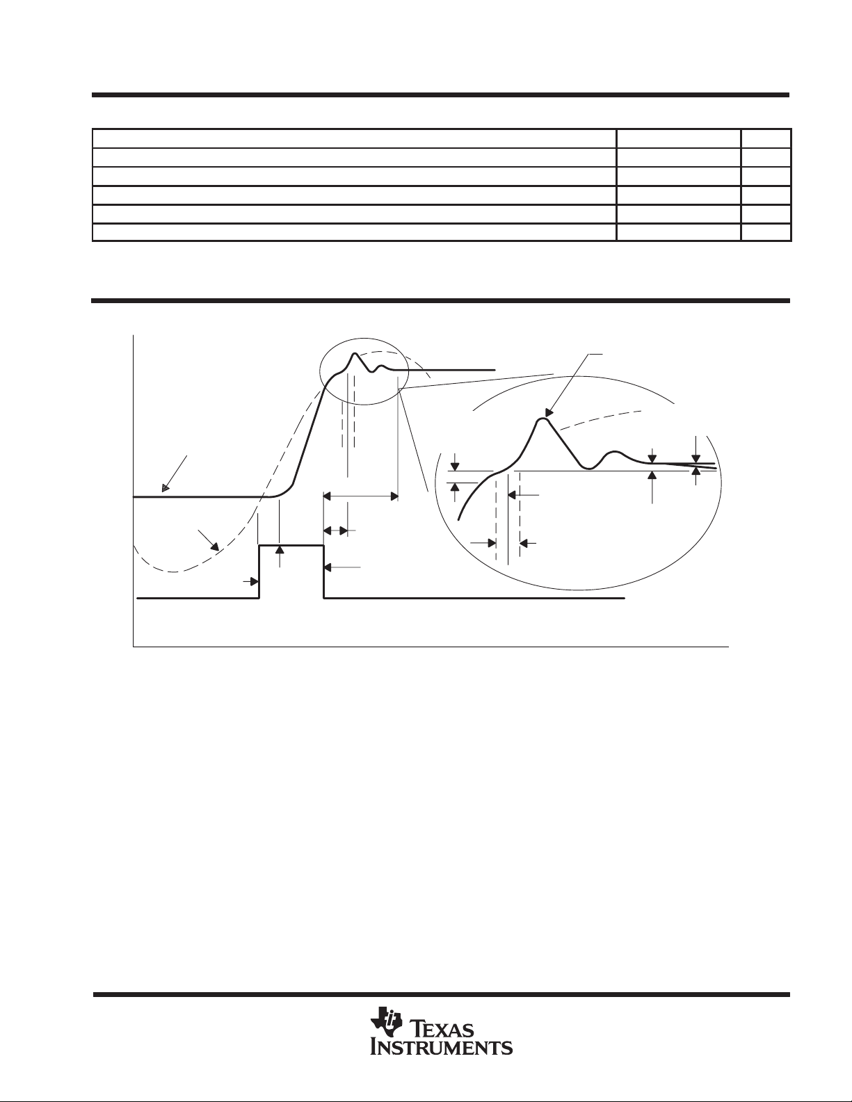
PARAMETER MEASUREMENT INFORMATION
Sample-to-Hold
Transient
Hold More
Voltage Droop
Sample-and-Hold
Output
Analog
Input
Signal
Sample
Command
Sample-Control Pulse
Sampling
Switch
Closes
(see Note A)
(see Note B)
Hold
Command
Aperture
Uncertainty
(error band)
Sample Switch
Opens
Aperture
Uncertainty
Time
Sample-to-Hold
Offset Error
Figure 1. Sample-Hold Definitions
NOTES: A. Hold-mode settling time is the time from the hold command transistion until the output has settled within a specified error band around
the final value.
B. Acquisition time is the time required, after the closing of the sampling switch, for the hold capacitor to charge to a full-scale voltage
change and then remain within a specified error band around the final value.
POST OFFICE BOX 655303 • DALLAS, TEXAS 75265
3
Page 4
TL1591
SAMPLE-AND-HOLD CIRCUIT FOR CCD IMAGERS
SOCS026B – SEPTEMBER 1989 – REVISED JUNE 1994
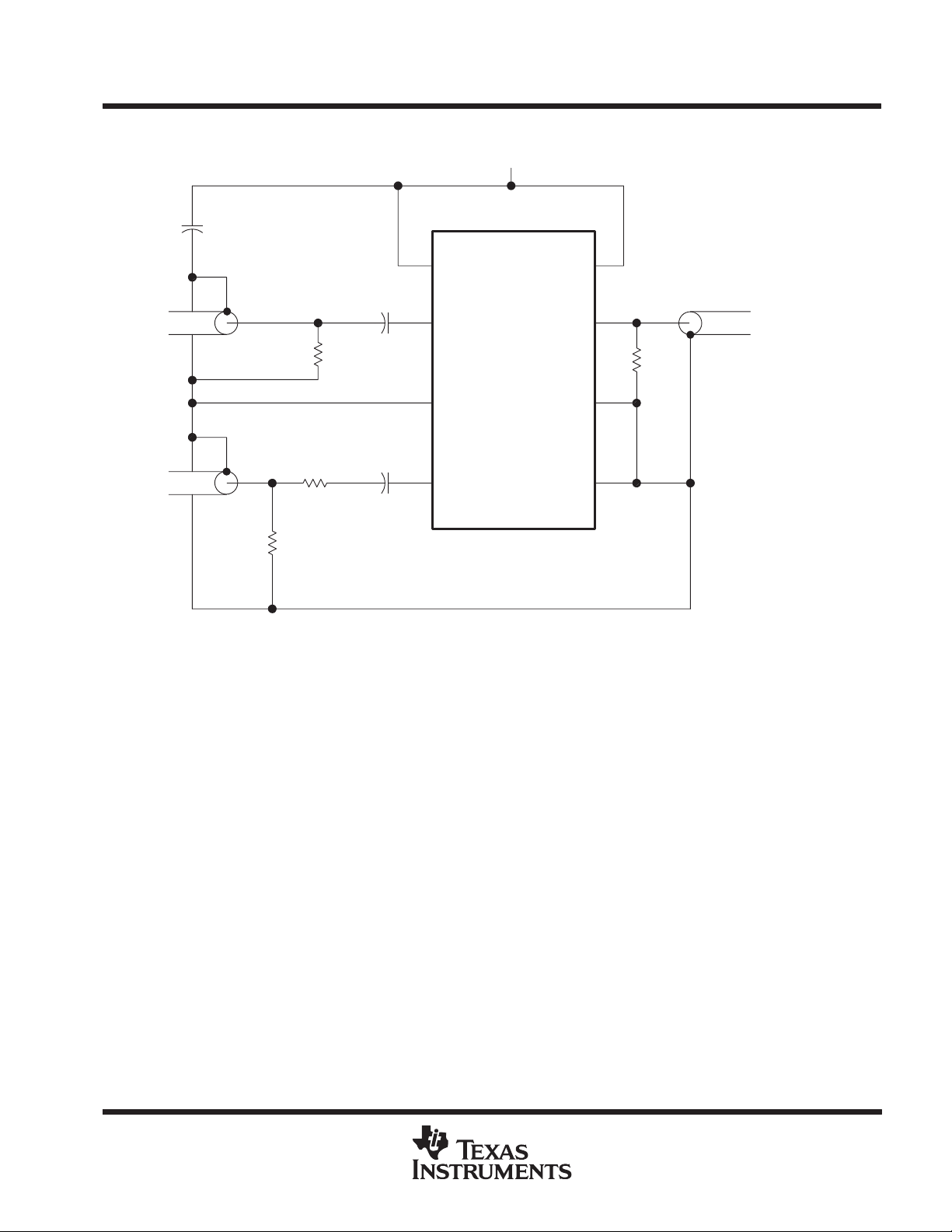
PARAMETER MEASUREMENT INFORMATION
V
CC
Analog
Input
Analog
Output
50 Ω
50 Ω
33 µF
53 Ω
975 Ω
50 Ω
1
ANLG V
33 µF
2
ANLG IN
3
ANLG GND
330 µF
4
ANLG OUT
Figure 2. Test Circuit
TL1591
CC
DGTL V
CC
DGTL IN
DGTL GND
SUB GND
8
7
50 Ω
6
5
50 Ω
Command Input
(sampling pulse)
4
POST OFFICE BOX 655303 • DALLAS, TEXAS 75265
Page 5
TL1591
SAMPLE-AND-HOLD CIRCUIT FOR CCD IMAGERS
SOCS026B – SEPTEMBER 1989 – REVISED JUNE 1994
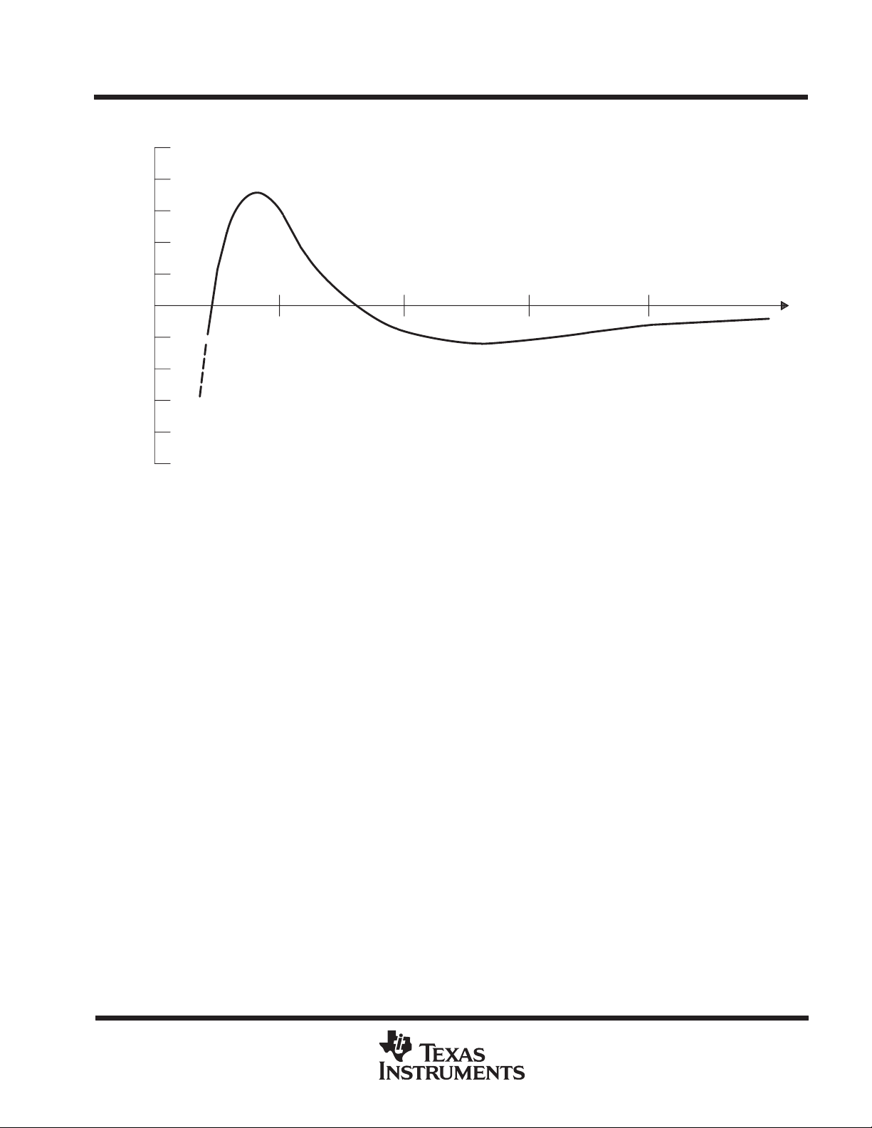
TYPICAL CHARACTERISTICS
5
4
3
2
1
0
–1
Sample/Hold Accuracy – %
–2
–3
–4
–5
20 30 40 50
Command Duration–ns
Figure 3. Sample/Hold Accuracy Versus Command Duration
POST OFFICE BOX 655303 • DALLAS, TEXAS 75265
5
Page 6

TL1591
SAMPLE-AND-HOLD CIRCUIT FOR CCD IMAGERS
SOCS026B – SEPTEMBER 1989 – REVISED JUNE 1994
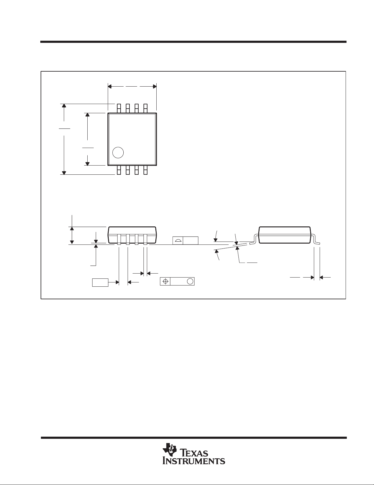
MECHANICAL DATA
P(R-PDIP-T8) PLASTIC DUAL-IN-LINE PACKAGE
0.400 (10,20)
MAX
58
0.260 (6,60)
0.240 (6,10)
14
0.070 (1,78) MAX
0.310 (7,87)
0.020 (0,51) MIN
0.290 (7,37)
0.200 (5,08) MAX
0.125 (3,18) MIN
0.100 (2,54) TYP
0.021 (0,53)
0.015 (0,38)
NOTES: A. All linear dimensions are in inches (millimeters).
B. This drawing is subject to change without notice.
Seating Plane
0°–15°
0.014 (0,36)
0.008 (0,20)
4040082/A–10/93
6
POST OFFICE BOX 655303 • DALLAS, TEXAS 75265
Page 7
TL1591
SAMPLE-AND-HOLD CIRCUIT FOR CCD IMAGERS
SOCS026B – SEPTEMBER 1989 – REVISED JUNE 1994
MECHANICAL DATA
PS/R-PDSO-G8 PLASTIC SMALL-OUTLINE PACKAGE
6,50
5,90
85
8,20
7,40
5,60
5,00
14
2,00 MAX
0,05 MIN
1,27
NOTES: A. All linear dimensions are in millimeters.
B. This drawing is subject to change without notice.
C. Body dimensions do not include mold flash or protrusion not to exceed 0,15.
Seating Plane
0,40
0,25
0,10
M
0°–10°
0,20
0,10
0,95
0,55
4040063/A–10/93
POST OFFICE BOX 655303 • DALLAS, TEXAS 75265
7
Page 8

IMPORTANT NOTICE
T exas Instruments and its subsidiaries (TI) reserve the right to make changes to their products or to discontinue
any product or service without notice, and advise customers to obtain the latest version of relevant information
to verify, before placing orders, that information being relied on is current and complete. All products are sold
subject to the terms and conditions of sale supplied at the time of order acknowledgement, including those
pertaining to warranty, patent infringement, and limitation of liability.
TI warrants performance of its semiconductor products to the specifications applicable at the time of sale in
accordance with TI’s standard warranty. Testing and other quality control techniques are utilized to the extent
TI deems necessary to support this warranty . Specific testing of all parameters of each device is not necessarily
performed, except those mandated by government requirements.
CERT AIN APPLICATIONS USING SEMICONDUCTOR PRODUCTS MAY INVOLVE POTENTIAL RISKS OF
DEATH, PERSONAL INJURY, OR SEVERE PROPERTY OR ENVIRONMENTAL DAMAGE (“CRITICAL
APPLICATIONS”). TI SEMICONDUCTOR PRODUCTS ARE NOT DESIGNED, AUTHORIZED, OR
WARRANTED TO BE SUITABLE FOR USE IN LIFE-SUPPORT DEVICES OR SYSTEMS OR OTHER
CRITICAL APPLICA TIONS. INCLUSION OF TI PRODUCTS IN SUCH APPLICATIONS IS UNDERST OOD TO
BE FULLY AT THE CUSTOMER’S RISK.
In order to minimize risks associated with the customer’s applications, adequate design and operating
safeguards must be provided by the customer to minimize inherent or procedural hazards.
TI assumes no liability for applications assistance or customer product design. TI does not warrant or represent
that any license, either express or implied, is granted under any patent right, copyright, mask work right, or other
intellectual property right of TI covering or relating to any combination, machine, or process in which such
semiconductor products or services might be or are used. TI’s publication of information regarding any third
party’s products or services does not constitute TI’s approval, warranty or endorsement thereof.
Copyright 1998, Texas Instruments Incorporated
 Loading...