TC281
1036- × 1010-PIXEL CCD IMAGE SENSOR
SOCS058B – JUNE 1996 – REVISED MA Y 1999
1
POST OFFICE BOX 655303 • DALLAS, TEXAS 75265
D
High-Resolution, Solid-State
Frame-Transfer Image Sensor
D
11.3-mm Image Area Diagonal
D
1000 (H) x 1000 (V) Active Elements
D
Up to 30 Frames per Second
D
8-µm Square Pixels
D
Low Dark Current
D
Advanced Lateral-Overflow-Drain
Antiblooming
D
Single Pulse Image Area Clear Capability
D
Dynamic Range ... More than 60 dB
D
High Sensitivity and Quantum Efficiency
D
Nondestructive Charge Detection Through
Texas Instruments (TI) Advanced BCD
Node Technology
D
High Near-IR and Blue Response
D
Solid-State Reliability With No Image
Burn-In, Residual Imaging, Image
Distortion, Image Lag, or Microphonics
description
The TC281 is a frame-transfer charge-coupled-device (CCD) image sensor that provides a very high-resolution
image acquisition capability for image-processing applications such as robotic vision, medical X-ray analysis,
and metrology. The image sensing area measures 8 mm horizontally and 8 mm vertically; the image-area
diagonal measures 1 1,3 mm and the sensor has 8-µm square pixels. The image area contains 1000 active lines
with 1000 active pixels per line. The dark reference signal can be obtained from ten dark reference lines located
between the image area and the storage area, 28 dark reference pixels located at the left edge of each horizontal
line, and 8 dark reference pixels located at the right edge of each horizontal line.
The storage section of the TC281 contains 1010 lines with 1036 pixels per line. The area is protected from
exposure to light by a metal layer. Photoelectric charge that is generated in the image area of the sensor can
be transferred into the storage section in less than 110 µs. After the image capture is completed (integration
time), the image readout is accomplished by transferring charge, one line at a time, into the serial register
located below the storage area. The serial register contains 1036 active pixels and 9 dummy pixels. The
maximum serial-register data rate is 40 megapixels per second. If the storage area needs to be cleared of all
charge, charge may be quickly transferred across the serial registers into the clearing drain located below the
register.
A high performance bulk charge detection (BCD) structure converts charge from each pixel into an output
voltage. A low-noise, two-stage, source-follower amplifier further buffers the signal before it is sent to the output
pin. A readout rate of 30 frames per second is easily achievable with this device.
The blooming-protection of the sensor is based on an advanced lateral-overflow-drain structure (ALOD). The
antiblooming function is activated when a suitable dc bias is applied to the overflow-drain pin. With this type of
blooming protection it is also possible to clear the image area of charge completely. This is accomplished by
providing a single 10V pulse of at least 1 µs duration to the overflow-drain pin.
Please be aware that an important notice concerning availability, standard warranty, and use in critical applications of
Texas Instruments semiconductor products and disclaimers thereto appears at the end of this data sheet.
PRODUCTION DATA information is current as of publication date.
Products conform to specifications per the terms of Texas Instruments
standard warranty. Production processing does not necessarily include
testing of all parameters.
Copyright 1999, Texas Instruments Incorporated
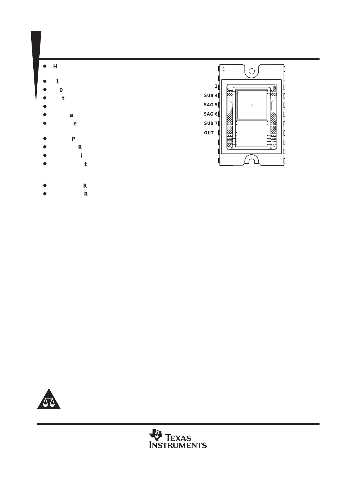
SUB 1
ODB 2
IAG 3
SUB 4
SAG 5
SAG 6
SUB 7
OUT 8
ADB 9
CDB 10
VGATE 11
22 SUB
21 TDB
20 IAG
19 SUB
18 SUB
17 SUB
16 NC
15 SRG
14 TRG
13 VSOURCE
12 RST
TI is a trademark of Texas Instruments Incorporated.
TC281
1036- × 1010-PIXEL CCD IMAGE SENSOR
SOCS058B – JUNE 1996 – REVISED MA Y 1999
2
POST OFFICE BOX 655303 • DALLAS, TEXAS 75265
description (continued)
The TC281 uses TI-proprietary advanced virtual-phase (A VP) technology , the advanced lateral-overflow-drain
structure, and the BCD detection node. These features provide the TI image sensing devices with a high blue
response, high near-IR sensitivity, low dark current, high photoresponse uniformity, and a single-phase
clocking. The TC281 is characterized for operation from -10_C to 45_C.
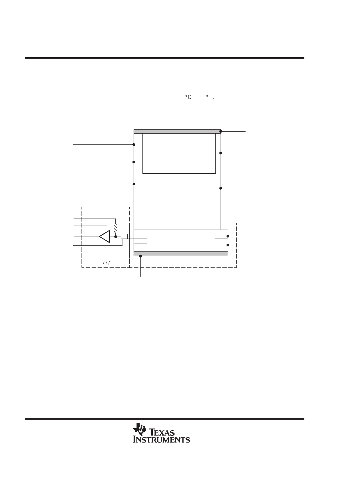
functional block diagram
Top Drain
Image Area
Storage Area
Serial Register
and Transfer Gate
Clearing Drain
21
20
5
15
14
TDB
10
11
12
88
9
13
Amplifier
6
3
2
ODB
IAG
SAG
V
SOURCE
ADB
OUT
RST
V
gate
CDB
IAG
SAG
SRG
TRG
ADVANCE INFORMATION
TC281
1036- × 1010-PIXEL CCD IMAGE SENSOR
SOCS058B – JUNE 1996 – REVISED MA Y 1999
3
POST OFFICE BOX 655303 • DALLAS, TEXAS 75265
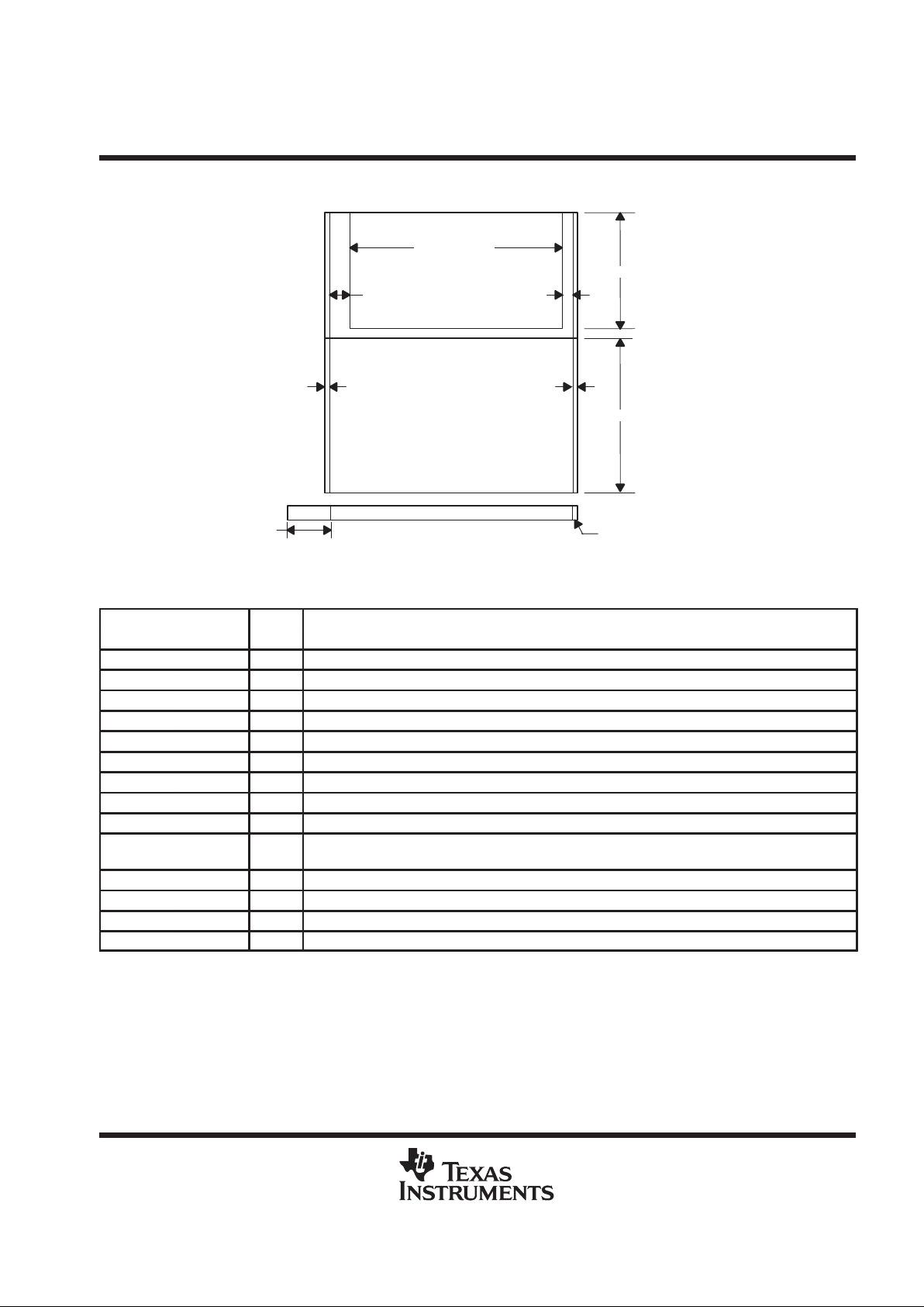
sensor topology diagram
1000 Pixels
28 Pixels 8 Pixels
1000 Lines
10 Lines
1010 Lines
1 Pixel1 Pixel
1 Dummy Pixel
10369
Dummy Pixels
Terminal Functions
TERMINAL
NAME NO.
I/O
DESCRIPTION
ADB 9 I Supply voltage for amplifier-drain bias
CDB 10 I Supply voltage for clearing-drain bias
IAG 3, 20 I Image area gate
NC 16 No connect
ODB 2 I Supply voltage overflow-drain antiblooming bias
OUT 8 O Output signal
RST 12 I Reset gate
SAG 5, 6 I Storage area gate
SRG 15 I Serial register gate 1
SUB
1, 4, 7, 17,
18, 19, 22
Substrate and clock return
TDB 21 NC Supply voltage for top-drain bias
TRG 14 I Transfer gate
VGATE 11 I Bias voltage for the gate of the BCD node
VSOURCE 13 I Bias voltage for the source of the BCD node
ADVANCE INFORMATION
TC281
1036- × 1010-PIXEL CCD IMAGE SENSOR
SOCS058B – JUNE 1996 – REVISED MA Y 1999
4
POST OFFICE BOX 655303 • DALLAS, TEXAS 75265
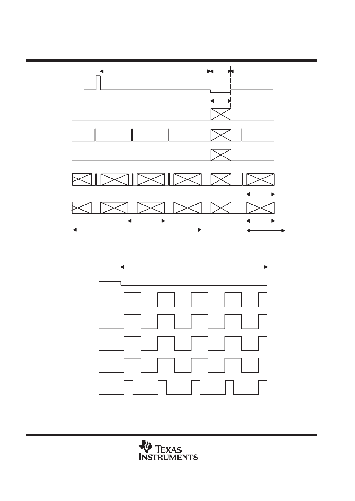
Integration Period Frame 2
Parallel Transfer
1010 Clocks
ODB
1046 Clocks
1010 Cycles
Readout Frame 2
Readout Frame 1
1046 Clocks
IAG
SAG
TRG
SRG
RST
Figure 1. Overview of Frame Timing with Variable Integration
Parallel Transfer 1010 Clocks
ODB
IAG
SAG
TRG
SRG
RST
Figure 2. Expanded Parallel Transfer Timing
ADVANCE INFORMATION

TC281
1036- × 1010-PIXEL CCD IMAGE SENSOR
SOCS058B – JUNE 1996 – REVISED MA Y 1999
5
POST OFFICE BOX 655303 • DALLAS, TEXAS 75265
1010 Cycles
Transfers One Line
From SA to SR
~1µs
Clears SRG During
Partial Line Readouts
Serial Line Readout
1046 Clocks
IAG
SAG
TRG
SRG
RST
Figure 3. Expanded Storage Area-to-Serial Register Transfer and Pixel Readout Timing
ODB
Storage Area Clear
9525 Clocks
IAG
SAG
TRG
SRG
RST
Figure 4. Special Modes of Operation: Storage Area Clear
ADVANCE INFORMATION
TC281
1036- × 1010-PIXEL CCD IMAGE SENSOR
SOCS058B – JUNE 1996 – REVISED MA Y 1999
6
POST OFFICE BOX 655303 • DALLAS, TEXAS 75265
IAG
~1µs
Transfer The
First Line From
SA to AR
Transfer The
Second Line
Adding to The First
Each Additional Pulse
Bins One Additional Line
Serial Line Readout
SAG
TRG
SRG
RST
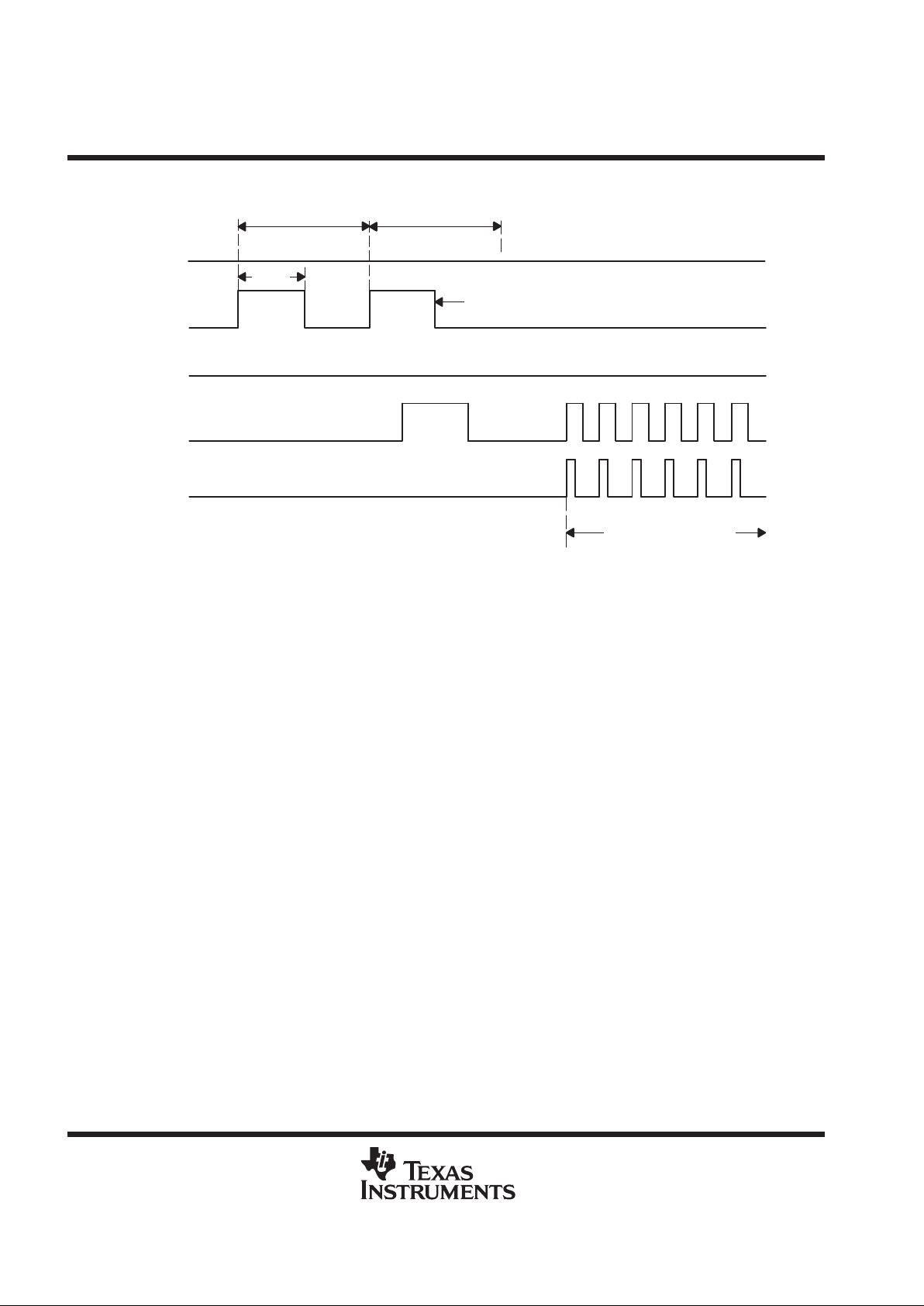
Figure 5. Special Modes of Operation: Binning
detailed description
The TC281 image sensor consists of five basic functional blocks: 1) the image-sensing area, 2) the advanced
lateral overflow drain (ALOD), 3) the storage area, 4) the serial register, and 5) the bulk charge detection (BCD)
node with the buffer output amplifier.
image-sensing area
The image-sensing area contains 1036 x 1010 pixel elements. A metal light shield covers 28 pixels on the left
edge of the sensing area, 8 pixels on the right edge, and 10 rows at the bottom of the sensing area. The dark
pixel signal can be used as a black reference during the video signal processing. The dark references will
accumulate the dark current at the same rate as the active photosites, thus representing the true black level
signal. As light enters the active photosites in the image area, electron hole pairs are generated and the
electrons are collected in the potential wells of the pixels. The wells have a finite charge storage capacity
determined by the pixel design. When the generated number of electrons in the illuminated pixels exceeds this
limit, the electrons could spill over into neighboring pixels and cause blooming. To prevent this problem, each
horizontal pair of pixels in the image sensing area shares a lateral overflow drain structure which provides up
to a 1000-to-1 protection against such undesirable phenomenon.
advanced lateral overflow drain
The advanced lateral overflow drain structure is shared by two neighboring pixels and provides several unique
features thus available in the sensor. By varying the dc bias of the drain pin, it is possible to control the blooming
protection level and trade it for the well capacity.
Applying a 10-V pulse for a minimum duration of 1 us above the nominal dc bias level causes charge in the image
area to be completely cleared. This feature permits a precise control of the integration time on a frame-by-frame
basis. The single-pulse clear capability also reduces smear by eliminating accumulated charge from the pixels
before the start of the integration (single sided smear).
ADVANCE INFORMATION

TC281
1036- × 1010-PIXEL CCD IMAGE SENSOR
SOCS058B – JUNE 1996 – REVISED MA Y 1999
7
POST OFFICE BOX 655303 • DALLAS, TEXAS 75265
advanced lateral overflow drain (continued)
Application of a negative 2-V pulse during the parallel transfer is recommended to prevent possible artifacts from
slight column-to-column pixel well capacity variations.
storage area
A metal light shield covers the storage area to prevent a further integration of charge when charge is being
stored before readout. When the sensor is to be used in a single-shot mode and is dormant for a long period
of time, it is necessary to perform multiple storage area clears to ensure the complete charge removal (see
Figure 4).
serial register
The serial register shifts the data out of the sensor area at a maximum rate of 40 MHz, thus achieving a 1000
x 1000 pixel readout with the frame rate of 30 frames per second. The data is shifted to the BCD node on the
falling edge of the SRG clocking pulses.
The data can also be transferred out of the serial registers in a parallel direction to the clear drain. This allows
partial line readouts. The timing for this operating mode consists of transferring the next row from the storage
into the serial register while also clocking the TRG gate. Binning of multiple pixels within a column together to
increase the device sensitivity is possible by multiple line transfers into the serial register prior to the register
readout. The timing for this mode of operation is shown in Figure 5. Care must be taken not to exceed the well
capacity of the serial register by transferring too many lines into it. Horizontal binning is also possible in this
sensor. It can be accomplished in the BCD detection node by a suitable skipping of the reset pulses.
bulk charge detection node and output amplifier
The TC281 image sensor uses a patented TI charge detection device called the bulk charge detection node.
In this structure, the signal electron packets are transferred under a uniquely designed p-channel MOS
transistor where they modulate the transistor threshold voltage. The threshold voltage changes are then
detected and represent the desired output signal. After sensing is completed, charge is removed from the node
by applying a reset pulse. One of the key advantages of the BCD charge detection concept is that charge is
sensed nondestructively . The nondestructive readout does not generate reset noise, therefore, eliminating the
need for the CDS post processing. Other advantages are high speed and a very low noise.
Emitter-follower output buffering is recommended for the TI image sensors. Also, it is recommended that the
emitter follower be ac coupled to the rest of the signal processing chain. AC coupling eliminates problems with
the sensor output dc stability and the sensor-to-sensor dc output level variations.
ADVANCE INFORMATION

TC281
1036- × 1010-PIXEL CCD IMAGE SENSOR
SOCS058B – JUNE 1996 – REVISED MA Y 1999
8
POST OFFICE BOX 655303 • DALLAS, TEXAS 75265
spurious nonuniformity specification
The spurious nonuniformity specification of the TC281 CCD grades –30 and –40 is based on several
performance characteristics:
D
Amplitude of the nonuniform line or pixel signal
D
Polarity of the nonuniform pixel signal
– Black
– White
D
Column signal amplitude
The CCD sensors are characterized in both an illuminated condition and a dark condition. In the dark condition,
the nonuniformity is specified in terms of absolute amplitude as shown in Figure 6. In the illuminated condition,
the nonuniformity is specified as a percentage of the total amplitude as shown in Figure 7.
PIXEL NONUNIFORMITY COLUMN NONUNIFORMITY
PART NUMBER
DARK CONDITION ILLUMINATED CONDITION
COLUMN AMPLITUDE
PIXEL AMPLITUDE, x (mV) % OF TOTAL ILLUMINATION
x (mV)
TC281-30 x ≤ TBD x ≤ TBD x < TBD
TC281-40 x ≤ TBD x ≤ TBD x ≤ TBD
mV
Amplitude
t
Illumination
% of Total
t
Figure 6. Pixel Nonuniformity, Figure 7. Pixel Nonuniformity,
Dark Condition Illuminated Condition
ADVANCE INFORMATION

TC281
1036- × 1010-PIXEL CCD IMAGE SENSOR
SOCS058B – JUNE 1996 – REVISED MA Y 1999
9
POST OFFICE BOX 655303 • DALLAS, TEXAS 75265
absolute maximum ratings over operating free-air temperature (unless otherwise noted)
†
Supply voltage range, V
CC
: ADB, CDB, TDB, Vgate, Vsource SUB to SUB + 15 V. . . . . . . . . . . . . . . . . . . . . .
Supply voltage range, V
CC
; ODB SUB to SUB + 21 V. . . . . . . . . . . . . . . . . . . . . . . . . . . . . . . . . . . . . . . . . . . . . . .
Clock voltage range: IAG, SAG, SRG, RST, TRG (see Note 1) –15 V to 15 V. . . . . . . . . . . . . . . . . . . . . . . . . .
Operating free-air temperature range, T
A
–10°C to 45°C. . . . . . . . . . . . . . . . . . . . . . . . . . . . . . . . . . . . . . . . . . . .
Storage temperature range, T
STG
–30°C to 85°C. . . . . . . . . . . . . . . . . . . . . . . . . . . . . . . . . . . . . . . . . . . . . . . . . . .
Package temperature for guaranteed operation –10°C to 55°C. . . . . . . . . . . . . . . . . . . . . . . . . . . . . . . . . . . . . . .
†
Stresses beyond those listed under “absolute maximum ratings” may cause permanent damage to the device. These are stress ratings only, and
functional operation of the device at these or any other conditions beyond those indicated under “recommended operating conditions” is not
implied. Exposure to absolute-maximum-rated conditions for extended periods may affect device reliability.
NOTE 1: Substrate at ground
recommended operating conditions
MIN NOM MAX UNIT
Supply voltage, V
CC
ADB, CDB 11 12 13 V
pp
Vsource 12 V
Suppl
y v
oltage, V
CC
Vgate 0 V
Image area clearing Vclear 14 16 18
Supply voltage for ODB
Antiblooming control Vabc 4 6 8
V
Parallel transfer Vxfer Vabc–2V
Supply current ADB 3.5 5 mA
Substrate bias voltage 0 V
High 1.5 2 2.5
Image area gate, IAG
Low –10.5 –10 –9.5
High 1.5 2 2.5
Storage area gate, SAG
Low –10.5 –10 –9.5
High 1.5 2 2.5
Clock voltage
Serial register gate, SRG
Low –10.5 –10 –9.5
V
High 1.5 2 2.5
Transfer gate, TRG
Low –10.5 –10 –9.5
High 5 5 8
Reset gate, RST
Low 0 0 0.5
IAG, SAG 5 10
Clock frequency, f
clock
SRG RST 40
MHz
TRG 5 10
ADVANCE INFORMATION

TC281
1036- × 1010-PIXEL CCD IMAGE SENSOR
SOCS058B – JUNE 1996 – REVISED MA Y 1999
10
POST OFFICE BOX 655303 • DALLAS, TEXAS 75265
electrical characteristics over recommended ranges of supply voltage and operating free-air
temperature
PARAMETER MIN TYP MAX UNIT
Dynamic range (see Note 2) 62 dB
Charge-conversion factor 10 µV/e
Charge-transfer efficiency (see Note 3) 0.99990 0.99995 1
Signal-response delay time, Tau (see Note 4) 7 ns
Output resistance 310 400 Ω
Noise-equivalent signal 12 25 electrons
Supply current (see Note 5) IDD 3.5 5 mA
IAG 14500
SAG 14500
Capacitance
SRG 52
pF
TRG 50
RST 5.5
†
All typical values are used at TA = 25°C.
NOTES: 2. Dynamic range is –20 times the logarithm of the mean-noise signal divided by the saturation-output signal.
3. Charge-transfer ef ficiency is one minus the charge loss per transfer in the output register. The test is performed in the dark using
an electrical input signal.
4. Signal-response delay time is the time between the falling edge of the SRG pulse and the output-signal valid state.
5. V
ADC
at 12 V and V
SUBSTRATE
at ground.
optical characteristics
PARAMETER MIN TYP MAX UNIT
No IR filter 240
Sensitivity (see Note 6)
With IR filter 30
mV/l
ux
Saturation signal, V
sat
(see Note 7) Antiblooming off 320 mV
Blooming overload ratio (see Note 8) 300 1000
Image-area well capacity 32K electrons
Smear at 5 MHz (see Notes 9 and 10) 0.06%
Dark current TA = 21°C 0.4 nA/cm
2
Electronic-shutter capability 1/1000 1/30 Saturation sec
NOTES: 6. Based on 16.67 ms integration time.
7. Saturation is the condition in which further increases in exposure do not lead to further increase in output signal.
8. Blooming-overload ratio is the ratio of blooming exposure to saturation exposure.
9. Smear is a measure of the error introduced by transferring charge through an illuminated pixel in shutterless operation. It is
equivalent to the ratio of the single-pixel transfer time to the exposure time using an illuminated section that is 1/10 of the image-area
vertical height with recommended clock frequencies.
10. The exposure time is 16.67 ms, the fast dump clocking rate during vertical timing is 10 MHz, and the illuminated section is 1/10 of
the height of the image section.
ADVANCE INFORMATION

TC281
1036- × 1010-PIXEL CCD IMAGE SENSOR
SOCS058B – JUNE 1996 – REVISED MA Y 1999
11
POST OFFICE BOX 655303 • DALLAS, TEXAS 75265
.15
.10
.05
0
300 500 700
Responsitivity – A/W
.20
.25
Wavelength – nm
RESPONSIVITY
vs
WAVELENGTH
.30
900
1100
Responsitivity
Figure 8. Typical Spectral Responsitivity
6
4
2
0
300 500 700
Sensitivity –
8
10
Wavelength – nm
12
900 1100
SENSITIVITY
vs
WAVELENGTH
Sensitivity
V
cm^2/µj
Figure 9. Typical Spectral Sensitivity
ADVANCE INFORMATION

TC281
1036- × 1010-PIXEL CCD IMAGE SENSOR
SOCS058B – JUNE 1996 – REVISED MA Y 1999
12
POST OFFICE BOX 655303 • DALLAS, TEXAS 75265
10
300 500 700
Quantium Efficiency – %
Wavelength – nm
QUANTUM EFFICIENCY
vs
WAVELENGTH
100
900 1100
Quantum Efficiency
Figure 10. Typical Spectral Quantum Efficiency
ADVANCE INFORMATION

TC281
1036- × 1010-PIXEL CCD IMAGE SENSOR
SOCS058B – JUNE 1996 – REVISED MA Y 1999
13
POST OFFICE BOX 655303 • DALLAS, TEXAS 75265
APPLICATION INFORMATION
NOTES: A. TI recommends designing AC coupled systems.
B. Inputs from user defined timer
C. Decoupling capacitors are not shown
1
22
3
4
5
6
7
8
9
10
11
22
21
20
19
18
17
16
15
14
13
12
SUB
ODB
IAG
SUB
SAG
SAG
SUB
OUT
ADB
CDB
VGATE
SUB
TDB
IAG
SUB
SUB
SUB
NC
SRG
TRG
VSOURCE
RST
AB_IN
CLR_IN
IAG_IN
SAG_IN
SRG_IN
TRG_IN
ODB
U2
Discrete ODB Driver
U3
U4
U1
IAG
SAG
Discrete Driver
RST_IN
SRG
TRG
RST
V
DD
V
DD
Discrete Serial Driver
AB
CLR
IAG
SAG
SRG
TRG
RST
ccd ANALOG OUT
(AC Coupled)
1
2
3
Q1
NPN
R2
100
R3
1 kΩ
C1
R1
100 kΩ
Figure 11. Typical Application Circuit
Table 1. Supply Voltages for Application Circuits
SUPPLY VOLTAGE
V
DD
12 V
V
CC
2 V
V
AA
–10 V
V
RST
5–8 V
ADVANCE INFORMATION

TC281
1036- × 1010-PIXEL CCD IMAGE SENSOR
SOCS058B – JUNE 1996 – REVISED MA Y 1999
14
POST OFFICE BOX 655303 • DALLAS, TEXAS 75265
APPLICATION INFORMATION
NOTES: A. MOSFET driver with a 4A peak current and 2 Ω output resistance (see Figure 14).
B. Image area clear (CLR) is active high while the parallel transfer (AB) is active low. These two pulses will generate the timing
for ODB, as shown in Figure 1.
C. Decoupling capacitors are not shown
+V
IN
U5
NC
+V
P-OUT
4A pk FET Driver
CLR
–V
–V
1
2
3
4
8
7
6
5
N-OUT
R6
0
C3
0.22 µF
0.22 µF
C2
+V
IN
U6
NC
+V
P-OUT
4A pk FET Driver
AB
–V
–V
1
2
3
4
8
7
6
5
N-OUT
R9
10
C5
0.22 µF
0.022 µF
C4
R7
200
KΩ
R5
1 kΩ
R4
3.83 kΩ
R8
3.24 kΩ
ODB
V
DD
V
DD
V
DD
Figure 12. T ypical ODB Driver Circuit
ADVANCE INFORMATION

TC281
1036- × 1010-PIXEL CCD IMAGE SENSOR
SOCS058B – JUNE 1996 – REVISED MA Y 1999
15
POST OFFICE BOX 655303 • DALLAS, TEXAS 75265
APPLICATION INFORMATION
NOTE A: Decoupling capacitors are not shown
2
31Q2
PFET
R12
5.1 Ω
R14
18 Ω
R11
392 Ω
R13
2 kΩ
D1
D2
3
1
2
Q3
NFET
R10
10 kΩ
R16
200 Ω
R15
10 kΩ
C6
0.22 µF
C7
0.22 µF
SRG_IN
V
CC
SRG
VAA
2
3
1
Q2
PFET
R12
5.1 Ω
R14
18 Ω
R11
392 Ω
R13
2 kΩ
D1
D2
3
1
2
Q3
NFET
R10
10 kΩ
R16
200 Ω
R15
10 kΩ
C6
0.22 µF
C7
0.22 µF
TRG_IN
V
CC
TRG
VAA
Figure 13. Typical Serial/Transfer Driver Circuits
2
3
1
Q2
PFET
R12
200 Ω
R14
200 Ω
R11
392 Ω
R13
2 kΩ
D1
D2
3
1
2
Q3
NFET
R10
10 kΩ
R16
200 Ω
R15
10 kΩ
C6
0.22 µF
C7
0.22 µF
RST_IN
VRST
RST
NOTE A: Decoupling capacitors are not shown
Figure 14. T ypical Reset Driver Circuit
ADVANCE INFORMATION

TC281
1036- × 1010-PIXEL CCD IMAGE SENSOR
SOCS058B – JUNE 1996 – REVISED MA Y 1999
16
POST OFFICE BOX 655303 • DALLAS, TEXAS 75265
APPLICATION INFORMATION
NOTES: A. MOSFET driver with a 4A peak current and 2 Ω output resistance (see Figure 13).
B. Decoupling capacitors are are not shown.
+V
IN
U7
NC
+V
P-OUT
4A pk FET Driver
–V
–V
1
2
3
4
8
7
6
5
N-OUT
V
CC
R17
806 Ω
R18
1 kΩ
3
1
2
Q4
PNP
IAG
IAG_IN
VAA
+V
IN
U8
NC
+V
P-OUT
4A pk FET Driver
–V
–V
1
2
3
4
8
7
6
5
N-OUT
V
CC
R19
806 Ω
R20
1 kΩ
3
1
2
Q5
PNP
SAG
SAG_IN
VAA
Figure 15. Typical Parallel Driver Circuit
ADVANCE INFORMATION

TC281
1036- × 1010-PIXEL CCD IMAGE SENSOR
SOCS058B – JUNE 1996 – REVISED MA Y 1999
17
POST OFFICE BOX 655303 • DALLAS, TEXAS 75265
MECHANICAL DATA
The package for the TC281 consists of a ceramic base, a glass window, and a 22-lead frame. The package leads
are configured in a dual in-line organization and fit into mounting holes with 2,54 mm (0.10 in) center-to-center
spacing. The glass window is sealed to the package by an epoxy adhesive. It can be cleaned by any standard
procedure for cleaning optical assemblies or by wiping the surface with a cotton swab moistened with alcohol.
Optical Center
Index Dot
Pin 1
Package
Center
7/96
17.90
17.40
9.51
9.21
28.22
27.66
25.13
24.87
16.60
16.40
1.00
0.90
0.508
2.10
1.70
1.12
0.92
3.22
2.62
18.03
17.53
0.30
0.20
0.76
0.16
5.10
3.50
0.56
0.46
2.67
2.41
Package
Center
0.08 ±0.08
0.08 ±0.08
TC281 (22 pin)
NOTES: A. All linear dimensions are in millimeters.
B. Single dimensions are nominal.
C. The center of the package and the center of the image area are not coincident.
D. Each pin centerline is located within 0,25 mm (0.010 in) of its true longitudinal position.
ADVANCE INFORMATION

IMPORTANT NOTICE
T exas Instruments and its subsidiaries (TI) reserve the right to make changes to their products or to discontinue
any product or service without notice, and advise customers to obtain the latest version of relevant information
to verify, before placing orders, that information being relied on is current and complete. All products are sold
subject to the terms and conditions of sale supplied at the time of order acknowledgement, including those
pertaining to warranty, patent infringement, and limitation of liability.
TI warrants performance of its semiconductor products to the specifications applicable at the time of sale in
accordance with TI’s standard warranty. Testing and other quality control techniques are utilized to the extent
TI deems necessary to support this warranty. Specific testing of all parameters of each device is not necessarily
performed, except those mandated by government requirements.
CERT AIN APPLICATIONS USING SEMICONDUCTOR PRODUCTS MAY INVOLVE POTENTIAL RISKS OF
DEATH, PERSONAL INJURY, OR SEVERE PROPERTY OR ENVIRONMENTAL DAMAGE (“CRITICAL
APPLICATIONS”). TI SEMICONDUCTOR PRODUCTS ARE NOT DESIGNED, AUTHORIZED, OR
WARRANTED TO BE SUITABLE FOR USE IN LIFE-SUPPORT DEVICES OR SYSTEMS OR OTHER
CRITICAL APPLICATIONS. INCLUSION OF TI PRODUCTS IN SUCH APPLICA TIONS IS UNDERST OOD TO
BE FULLY AT THE CUSTOMER’S RISK.
In order to minimize risks associated with the customer’s applications, adequate design and operating
safeguards must be provided by the customer to minimize inherent or procedural hazards.
TI assumes no liability for applications assistance or customer product design. TI does not warrant or represent
that any license, either express or implied, is granted under any patent right, copyright, mask work right, or other
intellectual property right of TI covering or relating to any combination, machine, or process in which such
semiconductor products or services might be or are used. TI’s publication of information regarding any third
party’s products or services does not constitute TI’s approval, warranty or endorsement thereof.
Copyright 1999, Texas Instruments Incorporated
 Loading...