

TC245
786- × 488-PIXEL CCD IMAGE SENSOR
SOCS019A – DECEMBER 1991
Copyright 1991, Texas Instruments Incorporated
2-1
POST OFFICE BOX 655303 • DALLAS, TEXAS 75265
• High-Resolution, Solid-State Image Sensor
for NTSC B/W TV Applications
• 8-mm Image-Area Diagonal, Compatible
With 1/2” Vidicon Optics
• 755 (H) x 242 (V) Active Elements in
Image-Sensing Area
• Advanced On-Chip Signal Processing
• Low Dark Current
• Electron-Hole Recombination Antiblooming
• Dynamic Range . . . More Than 70 dB
• High Sensitivity
• High Photoresponse Uniformity
• High Blue Response
• Single-Phase Clocking
• Solid-State Reliability With No Image
Burn-in, Residual Imaging, Image
Distortion, Image Lag, or Microphonics
description
The TC245 is a frame-transfer charge-coupled device (CCD) image sensor designed for use in single-chip B/W
NTSC TV applications. The device is intended to replace a 1/2-inch vidicon tube in applications requiring small
size, high reliability, and low cost.
The image-sensing area of the TC245 is configured into 242 lines with 786 elements in each line. Twenty-nine
elements are provided in each line for dark reference. The blooming-protection feature of the sensor is based
on recombining excess charge with charge of opposite polarity in the substrate. This antiblooming is activated
by supplying clocking pulses to the antiblooming gate, which is an integral part of each image-sensing element.
The sensor is designed to operate in an interlace mode, electronically displacing the image-sensing elements
in alternate fields by one-half of a vertical line during the charge integration period, effectively increasing the
vertical resolution and minimizing aliasing. The device can also be operated as a 755 (H) by 242 (V)
noninterlaced sensor with significant reduction in the dark signal.
A gated floating-diffusion detection structure with an automatic reset and voltage reference incorporated on-chip
converts charge to signal voltage. The signal is further processed by a low-noise, state-of-the-art correlated
clamp-sample-and-hold circuit. A low-noise, two-stage, source-follower amplifier buffers the output and
provides high output-drive capability . The image is read out through three outputs, each of which reads out every
third image column.
The TC245 is built using TI-proprietary virtual-phase technology, which provides devices with high blue
response, low dark signal, good uniformity , and single-phase clocking. The TC245 is characterized for operation
from –10°C to 45°C.
This MOS device contains limited built-in gate protection. During storage or handling, the device leads should be shorted together
or the device should be placed in conductive foam. In a circuit, unused inputs should always be connected to SUB. Under no
circumstances should pin voltages exceed absolute maximum ratings. Avoid shorting OUTn to ADB during operation to prevent
damage to the amplifier. The device can also be damaged if the output terminals are reverse-biased and an excessive current is
allowed to flow. Specific guidelines for handling devices of this type are contained in the publication
Guidelines for Handling
Electrostatic-Discharge-Sensitive (ESDS) Devices and Assemblies
available from Texas Instruments.
SUB 1
IAG 2
ABG 3
ADB 4
OUT3 5
OUT2 6
OUT1 7
AMP GND 8
CDB 9
SUB 10
20 SUB
19 IAG
18 ABG
17 SAG
16 SRG3
15 SRG2
14 SRG1
13 NC
12 TRG
11 IDB
DUAL-IN-LINE PACKAGE
(TOP VIEW)
NC – No internal connection
PRODUCTION DATA information is current as of publication date.
Products conform to specifications per the terms of Texas Instruments
standard warranty. Production processing does not necessarily include
testing of all parameters.
TC245
786- × 488-PIXEL CCD IMAGE SENSOR
SOCS019A – DECEMBER 1991
2-2
POST OFFICE BOX 655303 • DALLAS, TEXAS 75265
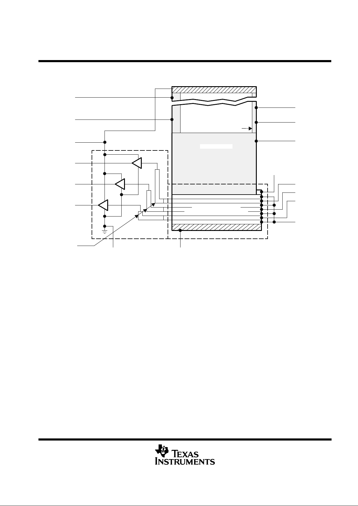
functional block diagram
Dark Reference Elements
Clearing Drain
Amplifiers
OUT2
OUT3
ADB
ABG
IAG
2
3
4
5
6
7
OUT1
8
AMP GND CDB
9
SRG3
SRG2
SRG1
TRG
IDB
12
14
15
16
SAG
17
ABG
IAG
18
19
Storage Area
Blooming Protection
Image Area With
Top Drain
11 Dummy
Elements
Gates, and Serial Registers
Multiplexer, Transfer
11
detailed description
The TC245 consists of four basic functional blocks: (1) the image-sensing area, (2) the image-storage area,
(3) the multiplexer block with serial registers and transfer gates, and (4) the low-noise signal-processing
amplifier block with charge-detection nodes. The location of each of these blocks is identified in the functional
block diagram.
TC245
786- × 488-PIXEL CCD IMAGE SENSOR
SOCS019A – DECEMBER 1991
2-3
POST OFFICE BOX 655303 • DALLAS, TEXAS 75265
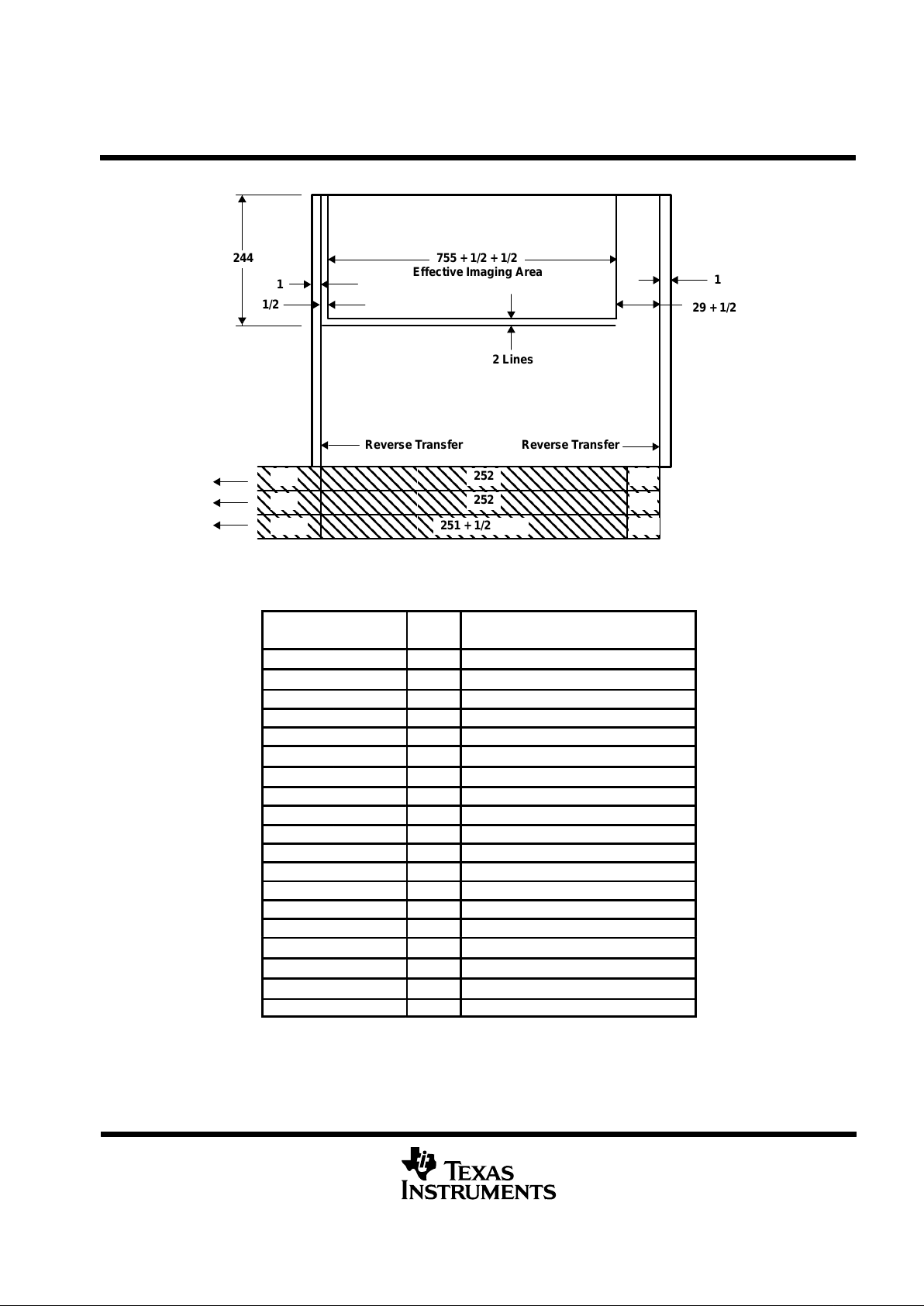
sensor topology diagram
1
1/2
244 755 + 1/2 + 1/2
Effective Imaging Area
1
29 + 1/2
2 Lines
Reverse Transfer Reverse Transfer
252
252
251 + 1/2 + 1/2
10
10
9.5
11
11
11.5
Dummy Pixels OPB
Terminal Functions
PIN
NAME NO.
I/O
DESCRIPTION
ABG
†
3 I Antiblooming gate
ABG
†
18 I Antiblooming gate
ADB 4 I Supply voltage for amplifier drain bias
AMP GND 8 Amplifier ground
CDB 9 I Supply voltage for clearing drain bias
IAG
†
2 I Image-area gate
IAG
†
19 I Image-area gate
IDB 11 I Supply voltage for input diode bias
OUT1 7 O Output signal 1
OUT2 6 O Output signal 2
OUT3 5 O Output signal 3
SAG 17 I Storage-area gate
SRG1 14 I Serial-register gate 1
SRG2 15 I Serial-register gate 2
SRG3 16 I Serial-register gate 3
SUB
†
1 Substrate and clock return
SUB
†
10 Substrate and clock return
SUB
†
20 Substrate and clock return
TRG 12 I Transfer gate
†
All pins of the same name should be connected together externally.

TC245
786- × 488-PIXEL CCD IMAGE SENSOR
SOCS019A – DECEMBER 1991
2-4
POST OFFICE BOX 655303 • DALLAS, TEXAS 75265
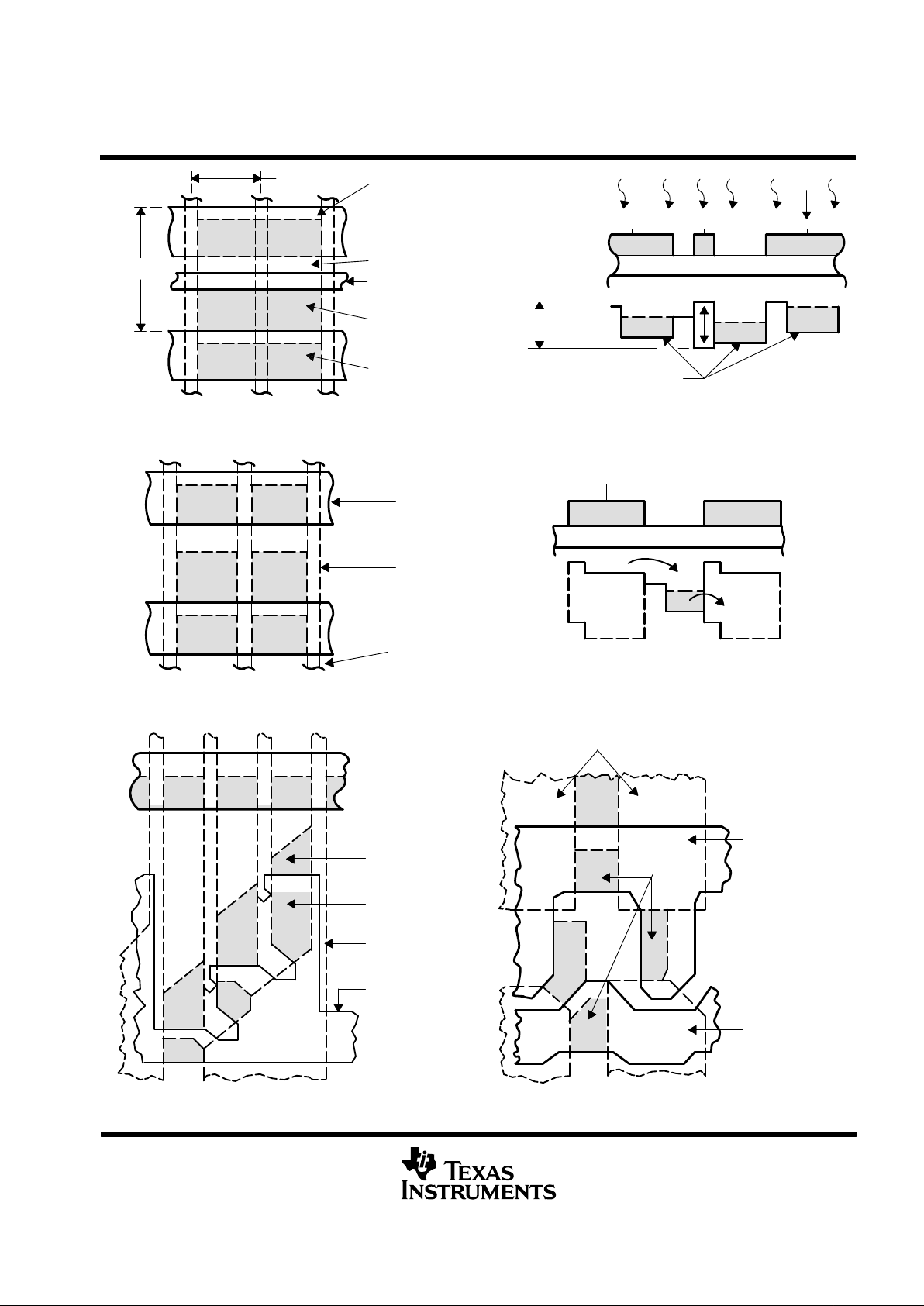
image-sensing and storage areas
Figure 1 and Figure 2 show cross sections with potential well diagrams and top views of image-sensing and
storage-area elements. As light enters the silicon in the image-sensing area, free electrons are generated and
collected in the potential wells of the sensing elements. During this time, blooming protection is activated by
applying a burst of pulses to the antiblooming gate inputs every horizontal blanking interval. This prevents
blooming caused by the spilling of charge from overexposed elements into neighboring elements. After
integration is complete, the signal charge is transferred into the storage area.
There are 29 full columns and one half-column of elements at the right edge of the image-sensing area that are
shielded from incident light; these elements provide the dark reference used in subsequent video processing
circuits to restore the video black level. There are also one full column and one half-column of light-shielded
elements at the left edge of the image-sensing area and two lines of light-shielded elements between the
image-sensing and image-storage areas (the latter prevent charge leakage from the image-sensing area into
the image-storage area).
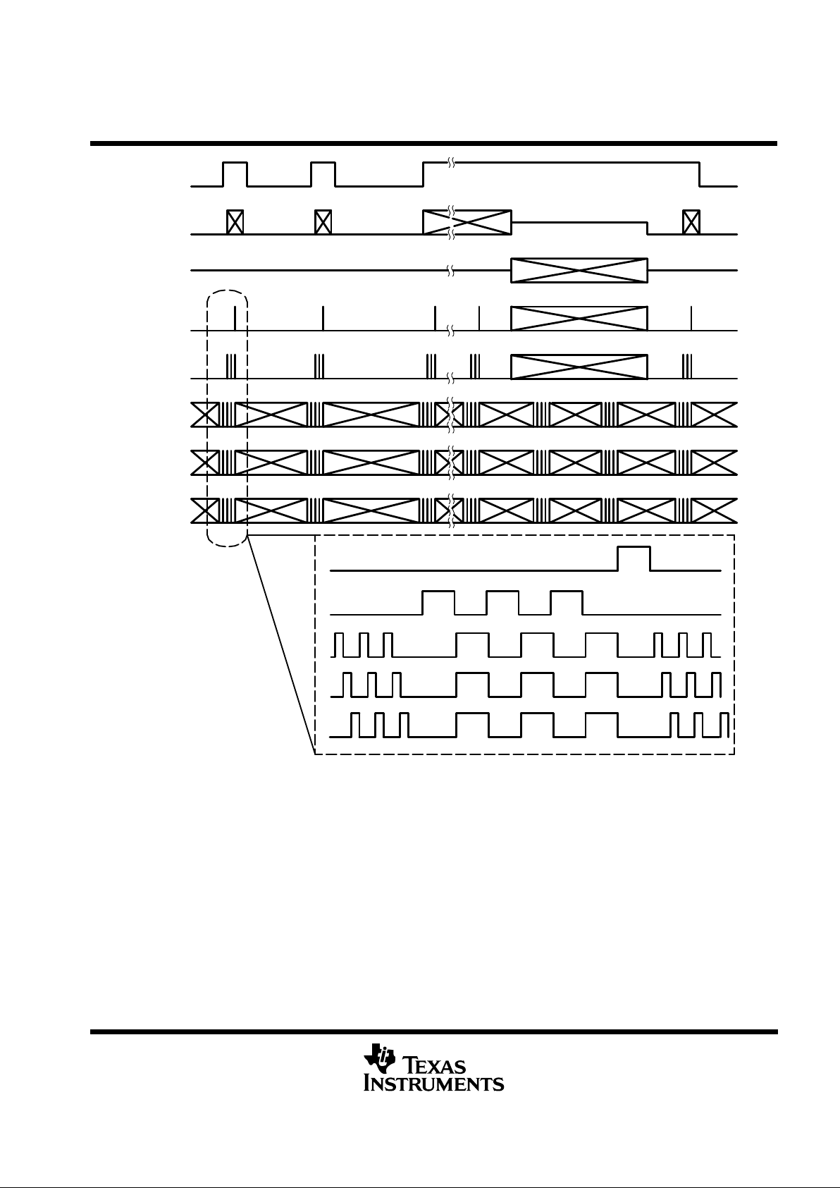
multiplexer with transfer gates and serial registers
The multiplexer and transfer gates transfer charge line by line from the storage-area columns into the
corresponding serial registers and prepare it for readout. Figure 3 illustrates the layout of the multiplexing gate
that vertically separates the pixels for input into the serial registers. Figure 4 shows the layout of the interface
region between the serial-register gates and the transfer gates. Multiplexing is activated during the horizontal
blanking interval by applying appropriate pulses to the transfer gates and serial registers; the required pulse
timing is shown in Figure 5. A drain is also included to provide the capability to clear the image-sensing and
storage areas of unwanted charge. Such charge can accumulate in the imager during the start-up of operation
or under special circumstances when nonstandard TV operation is desired.
correlated clamp-sample-and-hold amplifier with charge-detection nodes
Figure 6 illustrates the correlated clamp-sample-and-hold amplifier circuit. Charge is converted into a video
signal by transferring the charge onto a floating diffusion structure in detection node1 that is connected to the
gate of MOS transistor Q1. The proportional charge-induced signal is then processed by the circuit shown in
Figure 6. This circuit consists of a low-pass filter formed by Q1 and C2, coupling capacitor C1, dummy detection
node 2, which restores the dc bias on the gate of Q3, sampling transistor Q5, holding capacitor C3, and output
buffer Q6. Transistors Q2, Q4, and Q7 are current sources for each corresponding stage of the amplifier. The
parameters of this high-performance signal-processing amplifier have been optimized to minimize noise and
maximize the video signal.
The signal processing begins with a reset of detection node 1 and restoration of the dc bias on the gate of Q3
through the clamping function of dummy detection node 2. After the clamping is completed, the new charge
packet is transferred onto detection node 1. The resulting signal is sampled by the sampling transistor Q5 and
is stored on the holding capacitor C3. This process is repeated periodically and is correlated to the charge
transfer in the registers. The correlation is achieved automatically since the same clock lines used in registers
φ-S2 and φ-S3 for charge transport serve for reset and sample. The multiple use of the clock lines significantly
reduces the number of signals required to operate the sensor. The amplifier also contains an internal voltage
reference generator that provides the reference bias for the reset and clamp transistors. The detection nodes
and the corresponding amplifiers are located some distance away from the edge of the storage area. Therefore,
eleven dummy elements are incorporated at the end of each serial register to span the distance. The location
of the dummy elements, which are considered to be part of the amplifiers, is shown in the functional block
diagram.
TC245
786- × 488-PIXEL CCD IMAGE SENSOR
SOCS019A – DECEMBER 1991
2-5
POST OFFICE BOX 655303 • DALLAS, TEXAS 75265
φ-ABG
φ-IAG
8.5 µm(H)
Clocked Barrier
Virtual Barrier
Antiblooming Gate
Virtual Well
Clocked Well
Light
Antiblooming
Clocking Levels
Accumulated Charge
19.75 µm(V)
Figure 1. Charge-Accumulation Process
φ-PS
Channel Stops
Virtual Phase
Clocked Phase
Figure 2. Charge-Transfer Process
Gate
Multiplexing
Stop
Channel
Well
Clocked
Well
Virtual
Gate
Transfer
Serial-Register
Gate
Wells
Clocked
Channel Stops
Figure 3. Multiplexing-Gate Layout Figure 4. Interface-Region Layout
TC245
786- × 488-PIXEL CCD IMAGE SENSOR
SOCS019A – DECEMBER 1991
2-6
POST OFFICE BOX 655303 • DALLAS, TEXAS 75265
Composite
Blanking
SRG3
SRG2
SRG 1
TRG
SAG
IAG
ABG
Blanking Interval
Horizontal
Expanded
Figure 5. Timing Diagram

TC245
786- × 488-PIXEL CCD IMAGE SENSOR
SOCS019A – DECEMBER 1991
2-7
POST OFFICE BOX 655303 • DALLAS, TEXAS 75265
ADB
SRG1
Reset Gate
and
Output
Diode
Detection Node 1
CCD Register
Virtual
Gate
Clocked
Gate
Reference Generator
V
O
Q7
Q6
C3
Q5
Q4
Q3
Detection
Node 2
C2
C1
Q2
Q1
SRG2 SRG3
Figure 6. Correlated Clamp-Sample-and-Hold Amplifier Circuit Diagram

TC245
786- × 488-PIXEL CCD IMAGE SENSOR
SOCS019A – DECEMBER 1991
2-8
POST OFFICE BOX 655303 • DALLAS, TEXAS 75265
spurious nonuniformity specification
The spurious nonuniformity specification of the TC245 CCD grades –10, –20, –30, and –40 is based on several
sensor characteristics:
• Amplitude of the nonuniform pixel
• Polarity of the nonuniform pixel
– Black
– White
• Location of the nonuniformity (see Figure 7)
– Area A
– Element columns near horizontal center of the area
– Element rows near vertical center of the area
– Area B
– Up to the pixel or line border
– Up to area A
– Other
– Edge of the imager
– Up to area B
• Nonuniform pixel count
• Distance between nonuniform pixels
• Column amplitude
The CCD sensors are characterized in both an illuminated condition and a dark condition. In the dark condition,
the nonuniformity is specified in terms of absolute amplitude as shown in Figure 8. In the illuminated condition,
the nonuniformity is specified as a percentage of the total illumination as shown in Figure 9.
BA
20 Pixels
11
Lines
18 Pixels
Lines
7
377
Pixels
233
Lines
Figure 7. Sensor Area Map

TC245
786- × 488-PIXEL CCD IMAGE SENSOR
SOCS019A – DECEMBER 1991
2-9
POST OFFICE BOX 655303 • DALLAS, TEXAS 75265
mV
Amplitude
t
Illumination
% of Total
t
Figure 8. Pixel Nonuniformity, Figure 9. Pixel Nonuniformity,
Dark Condition Illuminated Condition
The grade specification for the TC245 is as follows (CCD video-output signal is 50 mV ±10 mV):
Pixel nonuniformity:
DARK CONDITION ILLUMINATED CONDITION
DISTANCE
NONUNIFORM PIXEL TYPE
DISTANCE
SEPARATION
PART
PIXEL
WHITE BLACK W/B
†
% OF TOTAL
TOTAL
NUMBER
AMPLITUDE
, x
(mV)
AREA AREA AREA
ILLUMINATION
AREA A
AREA B
COUNT‡
X Y AREA
(mV)
A B A B A B
TC245-20 x > 3.5 0 0 0 0 0 0 x > 5 0 0 — — — —
-
2.5 < x ≤ 3.5 2 5 2 5 2 5 5.0 < x ≤ 7.5 2 5
TC245-30
x > 3.5 0 0 0 0 0 0 x > 7.5 0 0
12
10080A
3.5 < x ≤ 7 3 7 3 7 3 7 7.5 < x ≤ 15 3 7
TC245-40
x > 7 0 0 0 0 0 0 x > 15 0 0
15
— — —
†
White and black nonuniform pixel pair
‡
The total spot count is the sum of all nonuniform white, black, and white/black pairs in the dark condition added to the number of nonuniform black
pixels in the illuminated condition. The sum of all nonuniform combinations will not exceed the total count.
Column nonuniformity:
PART
COLUMN
WHITE BLACK
PART
NUMBER
AMPLITUDE, x
AREAS AREAS
NUMBER
(mV)
AREAS
A AND B
AREAS
A AND B
TC245-20 x > 0.3 0 0
TC245-30 x > 0.5 0 0
TC245-40 x > 0.7 0 0

TC245
786- × 488-PIXEL CCD IMAGE SENSOR
SOCS019A – DECEMBER 1991
2-10
POST OFFICE BOX 655303 • DALLAS, TEXAS 75265
absolute maximum ratings over operating free-air temperature range (unless otherwise noted)
†
Supply voltage range for ADB, CDB, IDB (see Note 1) 0 V to 15 V. . . . . . . . . . . . . . . . . . . . . . . . . . . . . . . . . . . .
Input voltage range for ABG, IAG, SAG, SRG, TRG –15 V to 15 V. . . . . . . . . . . . . . . . . . . . . . . . . . . . . . . . . . .
Operating free-air temperature range, T
A
–30°C to 85°C. . . . . . . . . . . . . . . . . . . . . . . . . . . . . . . . . . . . . . . . . . . .
Storage temperature range –30°C to 85°C. . . . . . . . . . . . . . . . . . . . . . . . . . . . . . . . . . . . . . . . . . . . . . . . . . . . . . . . .
Lead temperature 1,6 mm (1/16 inch) from case for 10 seconds 260°C. . . . . . . . . . . . . . . . . . . . . . . . . . . . . . .
†
Stresses beyond those listed under “absolute maximum ratings” may cause permanent damage to the device. These are stress ratings only, and
functional operation of the device at these or any other conditions beyond those indicated under “recommended operating conditions” is not
implied. Exposure to absolute-maximum-rated conditions for extended periods may affect device reliability.
NOTE 1: All voltage values are with respect to the substrate terminal.
recommended operating conditions
MIN NOM MAX UNIT
Supply voltage, ADB 11 12 13 V
Substrate bias voltage 0 V
High level 1.5 2 2.5
IAG
Intermediate level
§
–5.7
Low level –11 –9
High level 1.5 2 2.5
SRG1, SRG2, SRG3
Low level –11 –9
High level 2 4 6
Input voltage, V
I
‡
ABG
Intermediate level
§
–2.3
V
Low level –7.5 –7 –6.5
High level 1.5 2 2.5
SAG
Low level –11 –9
High level 1.5 2 2.5
TRG
Low level –11 –9
IAG, SAG 3.58
Clock frequency, f
clock
SRG1, SRG2, SRG3, TRG 4.77
MHz
qy
clock
ABG 2
Capacitive load OUT1, OUT2, OUT3 6 pF
Operating free-air temperature, T
A
–10 45 °C
‡
The algebraic convention, in which the least-positive (most negative) value is designated minimum, is used in this data sheet for clock voltage
levels.
§
Adjustment is required for optimal performance.

TC245
786- × 488-PIXEL CCD IMAGE SENSOR
SOCS019A – DECEMBER 1991
2-11
POST OFFICE BOX 655303 • DALLAS, TEXAS 75265
electrical characteristics over recommended operating range of supply voltage, TA = –10°C to 45°C
PARAMETER MIN TYP
†
MAX UNIT
Dynamic range (see Note 2) Antiblooming disabled (see Note 3) 60 70 dB
Charge conversion factor 3.8 4 4.2 µV/e
Charge transfer efficiency (see Note 4) 0.99990 0.99995 1
Signal response delay time, τ (see Note 5 and Figure 13) 18 20 22 ns
Gamma (see Note 6) 0.97 0.98 0.99
Output resistance 700 800 Ω
1/f noise (5 kHz) 0.1
Noi
se voltage
Random noise (f = 100 kHz) 0.08
µV/√Hz
Noise equivalent signal 30 electrons
ADB (see Note 7) 20
Rejection ratio at 4.77 MHz SRG1, SRG2, SRG3 (see Note 8) 40 dB
ABG (see Note 9) 20
Supply current 5 mA
IAG 6500
SRG1, SRG2, SRG3 68
Input capacitance, C
i
ABG 2400 pF
TRG 180
SAG 6800
†
All typical values are at TA = 25 °C
NOTES: 2. Dynamic range is –20 times the logarithm of the mean noise signal divided by the saturation output signal.
3. For this test, the antiblooming gate must be biased at the intermediate level.
4. Charge transfer efficiency is one minus the charge loss per transfer in the output register. The test is performed in the dark using
an electrical input signal.
5. Signal-response delay time is the time between the falling edge of the SRG clock pulse and the output signal valid state.
6. Gamma (γ) is the value of the exponent in the equation below for two points on the linear portion of the transfer function curve (this
value represents points near saturation):
ǒ
Exposure (2)
Exposure (1)
Ǔ
g
+
ǒ
Output signal (2)
Output signal (1)
Ǔ
7. ADB rejection ratio is –20 times the logarithm of the ac amplitude at the output divided by the ac amplitude at ADB.
8. SRGn rejection ratio is –20 times the logarithm of the ac amplitude at the output divided by the ac amplitude at SRGn.
9. ABG rejection ratio is –20 times the logarithm of the ac amplitude at the output divided by the ac amplitude at ABG.

TC245
786- × 488-PIXEL CCD IMAGE SENSOR
SOCS019A – DECEMBER 1991
2-12
POST OFFICE BOX 655303 • DALLAS, TEXAS 75265
optical characteristics, TA = 40°C, integration time = 16.67 ms (unless otherwise noted)
PARAMETER MIN TYP MAX UNIT
No IR Filter
Measured at V
U
197
S
ens
itivit
y
With IR Filter
Measured at V
U
(see Notes 10 and 11)
24
m
V/l
x
Saturation signal, V
sat
(see Note 12) Antiblooming disabled, interlace off 320 mV
Maximum usable signal, V
use
Antiblooming enabled, interlace on 180 mV
Interlace on 100
Bl
ooming overload ratio (see Note
13)
Interlace off 200
Image-area well capacity 80 x 10
3
electrons
Smear (see Note 14) See Note 15 0.0004
Dark current Interlace off TA = 21°C 0.027 nA/cm
2
°
TC245-30 5.5
Dark si
gnal (see Note
16)
T
A
=
45°C
TC245-40 6
m
V
TC245-30 3.5
Pixel
uniformity
Output si
gnal = 50 mV
±10 mV
TC245-40 5
m
V
TC245-30 0.5
Col
umn uniformity
Output si
gnal = 50 mV
±10 mV
TC245-40 0.7
m
V
Shading Output signal = 100 mV 15%
NOTES: 10. Sensitivity is measured at an integration time of 16.67 ms with a source temperature of 2856 K. A CM-500 filter is used.
11. VU is the output voltage that represents the threshold of operation of antiblooming. VU ≈ 1/2 saturation signal.
12. Saturation is the condition in which further increase in exposure does not lead to further increase in output signal.
13. Blooming overload ratio is the ratio of blooming exposure to saturation exposure.
14. Smear is a measure of the error induced by transferring charge through an illuminated pixel in shutterless operation. It is equivalent
to the ratio of the single-pixel transfer time during a fast dump to the exposure time using an illuminated section that is 1/10 of the
image- area vertical height with recommended clock frequencies.
15. Exposure time is 16.67 ms, the fast-dump clocking rate during vertical timing is 3.58 MHz, and the illuminated section is 1/10 of the
height of the image section.
16. Dark-signal level is measured from the dummy pixels.

TC245
786- × 488-PIXEL CCD IMAGE SENSOR
SOCS019A – DECEMBER 1991
2-13
POST OFFICE BOX 655303 • DALLAS, TEXAS 75265
PARAMETER MEASUREMENT INFORMATION
DR (dynamic range)
+
camera white clip voltage
V
n
Vn = noise floor voltage
V
sat (min)
= minimum saturation voltage
V
use (max)
= maximum usable voltage
V
use (typ)
= typical user voltage (camera white clip)
(light input)
Lux
Enabled
With Antiblooming
Blooming Point
Well Capacity
Dependent On
Disabled
With Antiblooming
Blooming Point
Gate High Level
Upon Antiblooming
Level Dependent
DR
V
n
V
sat (min)
V
use (typ)
V
use (max)
V
O
NOTES: A. V
use (typ)
is defined as the voltage determined to equal the camera white clip. This voltage must be less than V
use (max)
.
B. A system trade-off is necessary to determine the system light sensitivity versus the signal/noise ratio. By lowering the V
use (typ)
,
the light sensitivity of the camera is increased; however, this sacrifices the signal/noise ratio of the camera.
Figure 10. Typical V
sat
, V
use
Relationship

TC245
786- × 488-PIXEL CCD IMAGE SENSOR
SOCS019A – DECEMBER 1991
2-14
POST OFFICE BOX 655303 • DALLAS, TEXAS 75265
PARAMETER MEASUREMENT INFORMATION
Slew rate between 10% and 90% = 70 to 120 V/µs, tr = 150 ns, tf = 90 ns.
t
f
t
r
0%
VIL max
10%
Intermediate Level
VIH min
90%
100%
Figure 11. Typical Clock Waveform for IAG, ABG and SAG
Slew rate between 10% and 90% = 300 V/µs, tr = tf = 15 ns.
t
f
t
r
0%
VIL max
10%
VIH min
90%
100%
Figure 12. Typical Clock Waveform for SRG and TRG
Hold
and
Sample
100%
90%
OUT
SRG
– 9 V
0%
– 9 V to –11 V
1.5 V to 2.5 V
CCD Delay
τ
15 ns10 ns
Figure 13. SRG and CCD Output Waveforms

TC245
786- × 488-PIXEL CCD IMAGE SENSOR
SOCS019A – DECEMBER 1991
2-15
POST OFFICE BOX 655303 • DALLAS, TEXAS 75265
TYPICAL CHARACTERISTICS
0.01
0.001
1
0.1
700 800 900
Responsivity – A/W
Incident Wavelength – nm
CCD SPECTRAL RESPONSIVITY
400 500 600 1000 1100
V
ADB
= 12 V, TA = 25°C
No IR Filter
Light Power = 1.5 µW/cm
2
Light Box: Canon SA702
Quantum Efficiency – %
100
60
50
40
30
20
10
5
3
2
300
Figure 14

TC245
786- × 488-PIXEL CCD IMAGE SENSOR
SOCS019A – DECEMBER 1991
2-16
POST OFFICE BOX 655303 • DALLAS, TEXAS 75265
APPLICATION INFORMATION
TC245
4.7 µF
+
+
+
+
15 pF
Oscillator
14.3-MHz
20 pF
4443424140393837363534
1
2
3
4
5
6
7
8
9
10
11
33
32
31
30
29
28
27
26
25
24
23
V
CC
1213141516171819202122
10 OUT1
11 OUT2
16
15
14
13
12 OUT3
1
2
3
4
5
6
7
8
ADB
10
20
19
18
17
16
15
14
13
12
11
1
2
3
4
5
6
7
8
9
V
ABG –
ABLVL
V
Parallel Driver
IALVL
V
SS
19
18
17
16
15
14
13
12
11
1
2
3
4
5
6
7
8
9
9
8
7
6
5
4
3
2
1
11
12
13
14
15
16
17
18
19
22 kΩ
47 kΩ
4.7 µF
4.7 µF
4.7 µF
100 Ω
100 Ω
100 Ω
9
ADB
V
CC
V
SS
V
ABLVL
IALVL
V
ABG+
V
ABG–
12 V
5 V
–10 V
2 V
–2.5 V
–5 V
4 V
–6 V
DC VOLTAGES
IALVL
I/N
IAIN
ABIN
MIDSEL
SAIN
PD
GND
V
ABG+
IASR
ABSR
V
CC
ABLVL
IAOUT
ABOUT
SAOUT
V
CC
V
ABG–
10
V
SS
V
SS
20
10
20
SEL0OUT
GND
PD
SRG3IN
SRG2IN
SRG1IN
TRGIN
NC
SEL1OUT
SEL0
NC
V
CC
SRG3OUT
SRG2OUT
SRG1OUT
TRGOUT
V
CC
SEL1V
SS
V
SS
V
ABG+
Serial Driver
SUB
IAG
ABG
SAG
SRG3
SRG2
SEG1
NC
TRG
IDB
SUB
IAG
ABG
ADB
OUT3
OUT2
OUT1
AMP GND
CDB
SUB
ANLG V
CC
AIN1
CIN1
AIN2
CIN2
AIN3
CIN3
ANLG GND
TL1593
S/H1
S/H2
S/H
3
DIG V
CC
OUT1
OUT2
OUT3
DGTL GND
V
CC
ABS1
ABS0
SC(90)
SC
BF
CBLK
CSYNC
CP1
CP2
BCP2
BCP1
T
S1
S2
S3
PD
PS
GT
ABIN
PI
MODE
GND
VCCV
CC
HIGH
GPS
SB
GP
VD
VD2
WHTA
VGATE
HGATE
CLK2M
VCC
FI
E/L
VDS
HCR
VCR
GT2
GT1/SH3
GT3/SH2
SH1
X2
X1
SN28835
NTSC Timer
TMS3473B
SN28846
Image Sensor
Sample-and-Hold
SUPPORT CIRCUITS
DEVICE PACKAGE APPLICATION FUNCTION
SN28835FS 44 pin flatpack T iming generator NTSC timing generator (CCD, S/H, processing)
SN28846DW 20 pin small outline Serial driver Driver for TRG, SRG1, SRG2, SRG3
TMS3473BDW 20 pin small outline Parallel driver Driver for IAG, SAG, ABG
TL1593CNS 16 pin small outline (EIAJ) Sample and hold Three-channel sample-and-hold IC
Figure 15. Typical Application Circuit Diagram

TC245
786- × 488-PIXEL CCD IMAGE SENSOR
SOCS019A – DECEMBER 1991
2-17
POST OFFICE BOX 655303 • DALLAS, TEXAS 75265
MECHANICAL DATA
The package for the TC245 consists of a ceramic base, a glass window, and a 20-lead frame. The glass window is
sealed to the package by an epoxy adhesive. The package leads are configured in a dual in-line organization and
fit into mounting holes with 1,78 mm (0.070 in) center-to-center spacings.
0,33 (0.013)
0,17 (0.007)
1,65 (0.065)
1,91 (0.075)
0,41 (0.016)
0,51 (0.020)
3,90 (0.154)
5,50 (0.217)
0,76 (0.030)
1,78 (0.070)
Rotation ±90°
7,20 (0.283)
7,60 (0.299)
Center
Package
Center
Optical
15,44 (0.608)
15,64 (0.616)
MAX
18,30 (0.720)
13,87 (0.546)
13,67 (0.538)
4,01 (0.158) MAX
15,54 (0.612)
14,94 (0.588)
1,70 (0.067)
1,10 (0.043)
Focus
Plane
6,50 (0.256)
6,10 (0.240)
ALL LINEAR DIMENSIONS ARE IN MILLIMETERS AND PARENTHETICALLY IN INCHES
TC245 (20 pin)
Index
Mark
7/94
15,14 (0.596)
14,84(0.584)
3,38(0.133)
2,72 (0.107)
NOTES: A. The center of the package and the center of image area not coincident.
B. The distance from the top of the glass to the image sensor surface is typically 1 mm (0.04 inch). The glass is 0.95 ±0.08 mm thick
and has an index of refraction of 1.53.
C. Each pin centerline is located within 0.18 mm of its true longitudinal position.
D. Maximum rotation of the sensor within the package is 1.5°.

SOCS019A – DECEMBER 1991
2-18
POST OFFICE BOX 655303 • DALLAS, TEXAS 75265

IMPORTANT NOTICE
T exas Instruments (TI) reserves the right to make changes to its products or to discontinue any semiconductor
product or service without notice, and advises its customers to obtain the latest version of relevant information
to verify, before placing orders, that the information being relied on is current.
TI warrants performance of its semiconductor products and related software to the specifications applicable at
the time of sale in accordance with TI’s standard warranty. Testing and other quality control techniques are
utilized to the extent TI deems necessary to support this warranty. Specific testing of all parameters of each
device is not necessarily performed, except those mandated by government requirements.
Certain applications using semiconductor products may involve potential risks of death, personal injury, or
severe property or environmental damage (“Critical Applications”).
TI SEMICONDUCTOR PRODUCTS ARE NOT DESIGNED, INTENDED, AUTHORIZED, OR WARRANTED
TO BE SUITABLE FOR USE IN LIFE-SUPPORT APPLICATIONS, DEVICES OR SYSTEMS OR OTHER
CRITICAL APPLICATIONS.
Inclusion of TI products in such applications is understood to be fully at the risk of the customer. Use of TI
products in such applications requires the written approval of an appropriate TI officer. Questions concerning
potential risk applications should be directed to TI through a local SC sales office.
In order to minimize risks associated with the customer’s applications, adequate design and operating
safeguards should be provided by the customer to minimize inherent or procedural hazards.
TI assumes no liability for applications assistance, customer product design, software performance, or
infringement of patents or services described herein. Nor does TI warrant or represent that any license, either
express or implied, is granted under any patent right, copyright, mask work right, or other intellectual property
right of TI covering or relating to any combination, machine, or process in which such semiconductor products
or services might be or are used.
Copyright 1995, Texas Instruments Incorporated
 Loading...