

TC237
680- × 500-PIXEL CCD IMAGE SENSOR
SOCS044B – JUNE 1994 – REVISED JUNE 1996
1
POST OFFICE BOX 655303 • DALLAS, TEXAS 75265
D
Very High-Resolution, 1/3-in Solid-State
Image Sensor for NTSC Black and White
Applications
D
340,000 Pixels per Field
D
Frame Memory
D
658 (H) × 496 (V) Active Elements in Image
Sensing Area Compatible With Electronic
Centerin
D
Multimode Readout Capability
– Progressive Scan
– Interlaced Scan
– Dual-Line Readout
– Image-Area Line Summing
– Smear Subtraction
D
Fast Single-Pulse Clear Capability
D
Continuous Electronic Exposure Control
From 1/60 – 1/50,000 s
D
7.4-µm Square Pixels
D
Advanced Lateral-Overflow-Drain
Antiblooming
D
Low Dark Current
D
High Dynamic Range
D
High Sensitivity
D
High Blue Response
D
Solid-State Reliability With No Image
Burn-In, Residual Imaging, Image
Distortion, Image Lag, or
Microphonics
description
The TC237 is a frame-transfer, charge-coupled device (CCD) image sensor designed for use in single-chip
black and white NTSC TV, computer, and special-purpose applications requiring low cost and small size.
The image-sensing area of the TC237 is configured into 500 lines with 680 elements in each line. Twenty-two
elements are provided in each line for dark reference. The blooming-protection feature of the sensor is based
on an advanced lateral-overflow-drain concept. The sensor can be operated in a true-interlace mode as a
658(H) × 496(V) sensor with a very low dark current. One important feature of the TC237 very high-resolution
sensor is the ability to capture a full 340,000 pixels per field. The image sensor also provides high-speed imagetransfer capability. This capability allows for a continuous electronic exposure control without the loss of
sensitivity and resolution inherent in other technologies. The charge is converted to signal voltage at 20 µV per
electron by a high-performance structure with a reset and a voltage-reference generator. The signal is further
buffered by a low-noise, two-stage, source-follower amplifier to provide high output-drive capability.
The TC237 is built using TI-proprietary advanced virtual-phase (A VP) technology , which provides devices with
high blue response, low dark signal, good uniformity, and single-phase clocking. The TC237 is characterized
for operation from –10°C to 45°C.
This MOS device contains limited built-in gate protection. During storage or handling, the device leads should be shorted together
or the device should be placed in conductive foam. In a circuit, unused inputs should always be connected to VSS. Under no
circumstances should pin voltages exceed absolute maximum ratings. Avoid shorting OUT to VSS during operation to prevent
damage to the amplifier. The device can also be damaged if the output terminals are reverse-biased and an excessive current is
allowed to flow. Specific guidelines for handling devices of this type are contained in the publication
Guidelines for Handling
Electrostatic-Discharge-Sensitive (ESDS) Devices and Assemblies
available from Texas Instruments.
Copyright 1996, Texas Instruments Incorporated
PRODUCTION DATA information is current as of publication date.
Products conform to specifications per the terms of Texas Instruments
standard warranty. Production processing does not necessarily include
testing of all parameters.
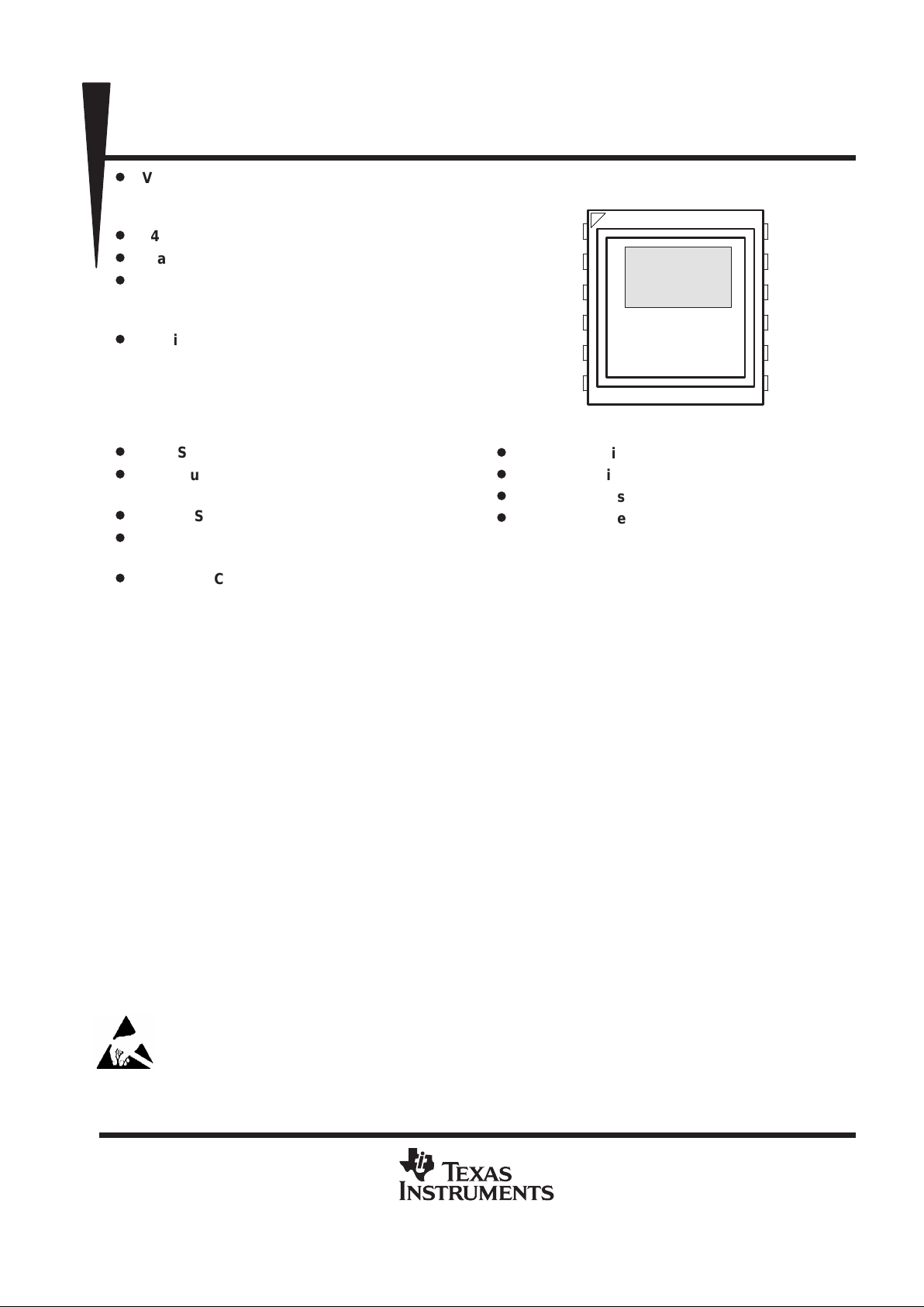
DUAL-IN-LINE PACKAGE
(TOP VIEW)
ODB 1
IAG2 2
SUB 3
ADB 4
OUT1 5
OUT2 6
12 IAG1
11 SAG
10 SAG
9 SUB
8 SRG
7 RST
TC237
680- × 500-PIXEL CCD IMAGE SENSOR
SOCS044B – JUNE 1994 – REVISED JUNE 1996
2
POST OFFICE BOX 655303 • DALLAS, TEXAS 75265
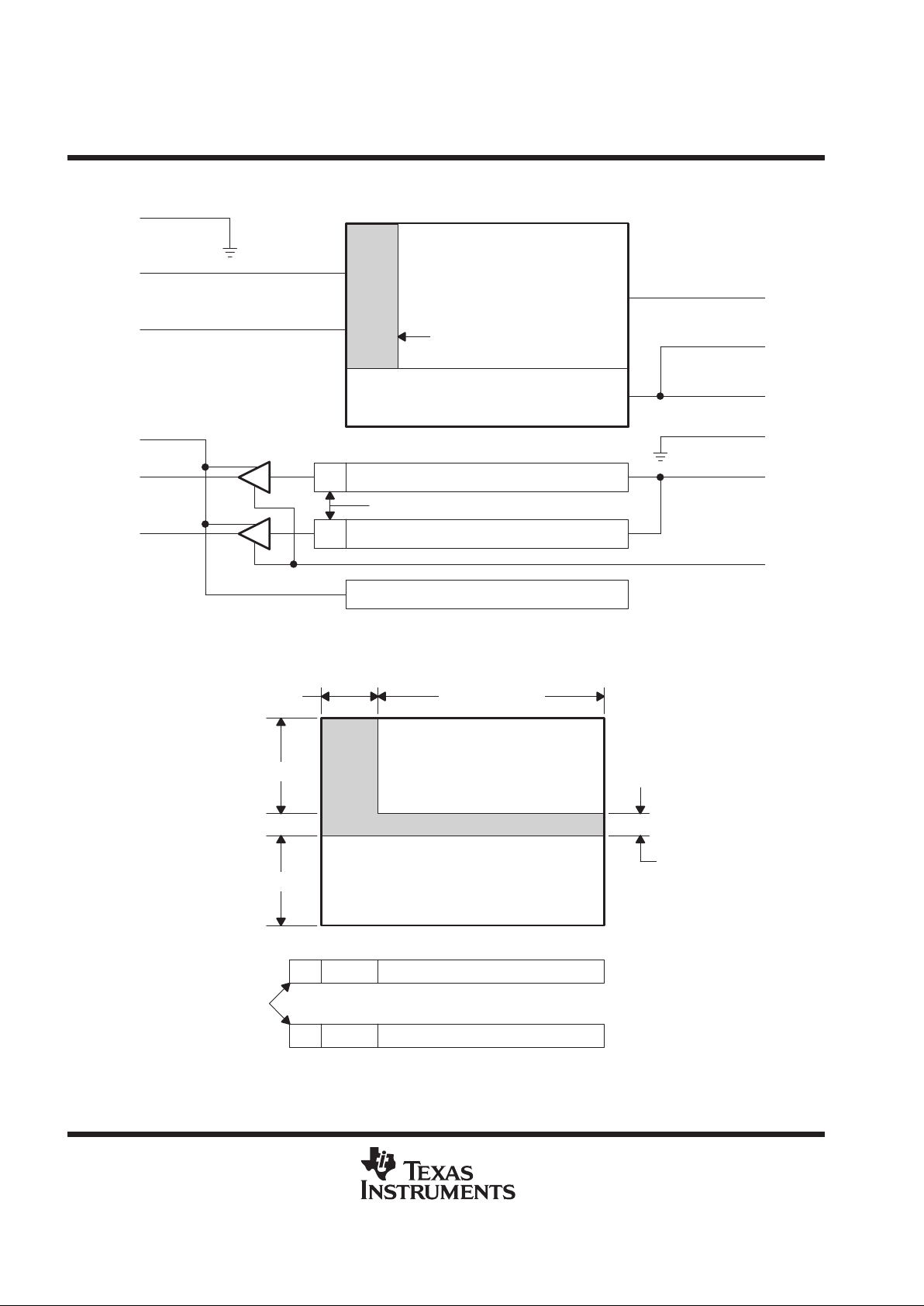
functional block diagram
Image Area With
Blooming Protection
Dark Reference Elements
Storage Area
Clearing Drain
3
1
2
4
6
5
SUB
ODB
IAG2
ADB
OUT2
OUT1
Amplifiers
4 Dummy Elements
9
8
7
10
12
11
IAG1
SAG
SAG
SUB
SRG
RST
sensor topology diagram
Single-Phase Storage Area
Two-Phase Image-Sensing Area
422
Optical Black
(OPB)
4 22 658 Active Pixels
Dummy Pixels
658 Active Pixels
4 Dark Lines
22 Dark Reference Pixels
658 Active Pixels
496 Lines
500 Lines

TC237
680- × 500-PIXEL CCD IMAGE SENSOR
SOCS044B – JUNE 1994 – REVISED JUNE 1996
3
POST OFFICE BOX 655303 • DALLAS, TEXAS 75265
Terminal Functions
TERMINAL
NAME NO.
I/O
DESCRIPTION
ADB 4 I Supply voltage for amplifier-drain bias
IAG1 12 I Image-area gate 1
IAG2 2 I Image-area gate 2
ODB 1 I Supply voltage overflow-drain antiblooming bias
OUT1 5 O Output signal 1
OUT2 6 O Output signal 2
RST 7 I Reset gate
SAG 10, 11 I Storage-area gate
SRG 8 I Serial-register gate
SUB 3, 9 Substrate
detailed description
The TC237 consists of four basic functional blocks: the image-sensing area, the image-storage area, the serial
register gates, and the low-noise signal processing amplifier block with charge-detection nodes and
independent resets. The location of each of these blocks is identified in the functional block diagram.
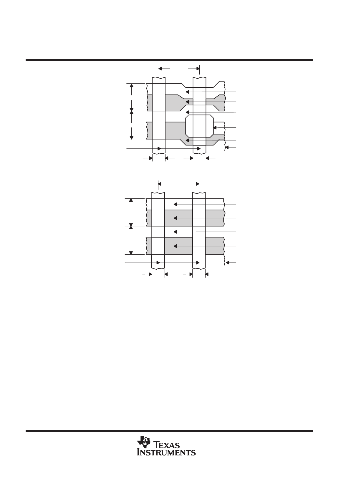
image-sensing and storage areas
Figure 1 and Figure 2 show cross sections with potential-well diagrams and top views of the image-sensing and
storage-area elements. As light enters the silicon in the image-sensing area, free electrons are generated and
collected in the wells of the sensing elements. Blooming protection is provided by applying a dc bias to the
overflow-drain bias pin. If it is necessary to clear the image before beginning a new integration time (for
implementation of electronic fixed shutter or electronic auto-iris), it is possible to do so by applying a pulse at
least 1 µs in duration to the overflow-drain bias. After integration is complete, the charge is transferred into the
storage area; the transfer timing is dependent on whether the readout mode is interlace or progressive scan.
If the progressive-scan readout mode is selected, the readout may be performed normally by utilizing one serial
register or high speed by using both serial registers (see Figure 3 through Figure 5). A line-summing operation
(which is useful in off-chip smear subtraction) may be implemented before the parallel transfer (see Figure 6
for line-summing timing).
There are 22 columns at the left edge of the image-sensing area that are shielded from incident light; these
elements provide the dark reference used in subsequent video-processing circuits to restore the video black
level. There are also four dark lines between the image-sensing and the image-storage area that prevent charge
leakage from the image-sensing area into the image-storage area.
TC237
680- × 500-PIXEL CCD IMAGE SENSOR
SOCS044B – JUNE 1994 – REVISED JUNE 1996
4
POST OFFICE BOX 655303 • DALLAS, TEXAS 75265
3.8 µm
3.6 µm
7.4 µm
1.6 µm
1.6 µm
Channel Stops
Including Metal Bus Lines
Clocked Barrier
Clocked Well
Virtual Barrier
Antiblooming
Device
Virtual Well
Clocked Gate
Figure 1. Image-Area Pixel Structure
3.5 µm
3.5 µm
7.4 µm
1.6 µm
Clocked Barrier
Clocked Well
Virtual Barrier
Virtual Well
Clocked Gate
1.6 µm
Channel Stops
Including Metal Bus Lines
Figure 2. Storage-Area Pixel Structure
TC237
680- × 500-PIXEL CCD IMAGE SENSOR
SOCS044B – JUNE 1994 – REVISED JUNE 1996
5
POST OFFICE BOX 655303 • DALLAS, TEXAS 75265
Expanded Section of
Parallel Transfer
IAG1, 2
SAG
SRG
1 µs Minimum
684 Pulses
684 Pulses
†
†
†
‡
ODB
IAG1, 2
SAG
SRG
RST
Clear Integrate Transfer to Memory Readout
250 Cycles
Figure 3. Interlace Timing
†
The number of parallel transfer pulses is field dependent. Field 1 has 500 pulses of IAG1, IAG2, SAG, and SRG with appropriate phasing. Field 2
has 501 pulses.
‡
The readout is from register 2.

TC237
680- × 500-PIXEL CCD IMAGE SENSOR
SOCS044B – JUNE 1994 – REVISED JUNE 1996
6
POST OFFICE BOX 655303 • DALLAS, TEXAS 75265
Expanded Section of
Parallel Transfer
IAG1, 2
SAG
SRG
1 µs Minimum
684 Pulses
†
684 Pulses
ODB
IAG1, 2
SAG
SRG
RST
Clear Integrate Transfer to Memory Readout
500 Cycles
500 Pulses
500 Pulses
500 Pulses
†
The readout will be from register 2.
Figure 4. Progressive-Scan Timing With Single Register Readout

TC237
680- × 500-PIXEL CCD IMAGE SENSOR
SOCS044B – JUNE 1994 – REVISED JUNE 1996
7
POST OFFICE BOX 655303 • DALLAS, TEXAS 75265
Expanded Section of
Parallel Transfer
IAG1, 2
SAG
SRG
1 µs Minimum
684 Pulses
684 Pulses
ODB
IAG1, 2
SAG
SRG
RST
Clear Integrate Transfer to Memory Readout
250 Cycles
500 Pulses
500 Pulses
500 Pulses
Figure 5. Progressive-Scan Timing With Dual Register Readout

TC237
680- × 500-PIXEL CCD IMAGE SENSOR
SOCS044B – JUNE 1994 – REVISED JUNE 1996
8
POST OFFICE BOX 655303 • DALLAS, TEXAS 75265
Expanded Section of
Parallel Transfer
IAG1, 2
SAG
SRG
1 µs Minimum
684 Pulses
684 Pulses
§
ODB
IAG2
SAG
SRG
RST
Clear Integrate Transfer to Memory Readout
250 Cycles
†
IAG1
Line
Sum
‡
¶
¶
¶
¶
Figure 6. Line-Summing Timing
†
This pulse occurs only during field 1.
‡
This pulse occurs only during field 2.
§
While readout is from register 2, register 1 can be read out for off-chip smear subtraction.
¶
The number of parallel transfer pulses if field dependent. field 1 has 500 pulses and field 2 has 501 pulses.

TC237
680- × 500-PIXEL CCD IMAGE SENSOR
SOCS044B – JUNE 1994 – REVISED JUNE 1996
9
POST OFFICE BOX 655303 • DALLAS, TEXAS 75265
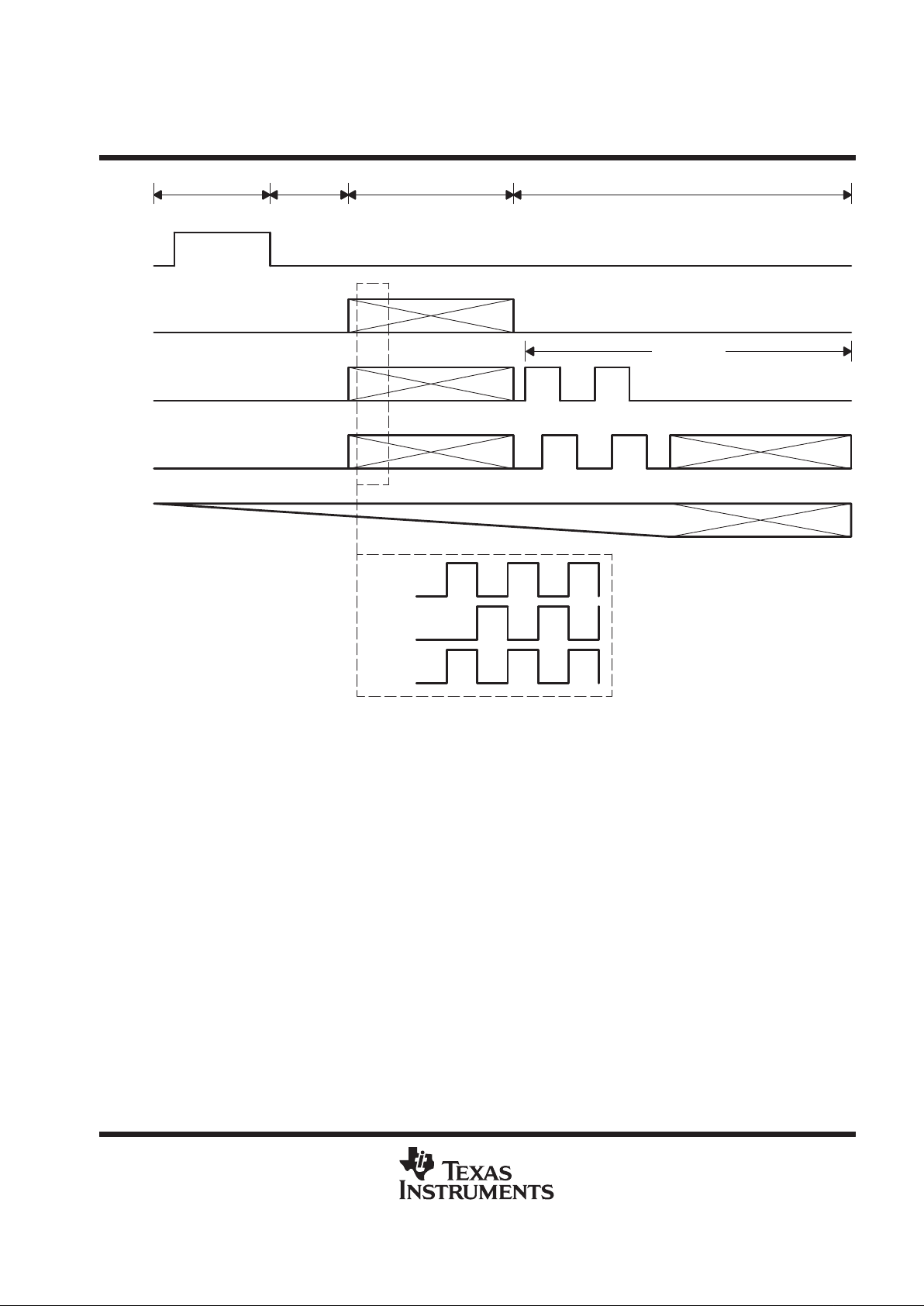
serial registers
The storage-area gate and serial gate(s) are used to transfer the charge line by line from the storage area into
the serial register(s). Depending on the readout mode, one or both serial registers is used. If both are used, the
registers are read out in parallel.
readout and video processing
After transfer into the serial register(s), the pixels are clocked out and sensed by a charge-detection node. The
node must be reset to a reference level before the next pixel is placed onto the detection node. The timing for
the serial-register readout, which includes the external pixel clamp and sample-and-hold signals needed to
implement correlated double sampling, is shown in Figure 7. As the charge is transferred onto the detection
node, the potential of this node changes in proportion to the amount of signal received. The change is sensed
by an MOS transistor and, after proper buffering, the signal is supplied to the output terminal of the image sensor .
The buffer amplifier converts charge into a video signal. Figure 8 shows the circuit diagram of the
charge-detection node and output amplifier. The detection nodes and amplifiers are placed a short distance
away from the edge of the storage area; therefore, each serial register contains 4 dummy elements that are used
to span the distance between the serial registers and the amplifiers.
OUT
RST
SRG
S/H
PCMP
Figure 7. Serial-Readout and Video-Processing Timing
V
OUT
ADBV
REF
Reset
CCD Channel
QR Q1 Q2
Figure 8. Output Amplifier and Charge-Detection Node

TC237
680- × 500-PIXEL CCD IMAGE SENSOR
SOCS044B – JUNE 1994 – REVISED JUNE 1996
10
POST OFFICE BOX 655303 • DALLAS, TEXAS 75265
absolute maximum ratings over operating free-air temperature range (unless otherwise noted)
†
Supply voltage range, ADB (see Note 1) SUB to SUB + 15 V. . . . . . . . . . . . . . . . . . . . . . . . . . . . . . . . . . . . . . . . .
Supply voltage range, ODB SUB to SUB + 21 V. . . . . . . . . . . . . . . . . . . . . . . . . . . . . . . . . . . . . . . . . . . . . . . . . . . .
Input voltage range for ABG, IAG1, IAG2, SAG, SRG 0 V to 15 V. . . . . . . . . . . . . . . . . . . . . . . . . . . . . . . . . . . . .
Operating free-air temperature range, T
A
–10°C to 45°C. . . . . . . . . . . . . . . . . . . . . . . . . . . . . . . . . . . . . . . . . . . .
Storage temperature range –30°C to 85°C. . . . . . . . . . . . . . . . . . . . . . . . . . . . . . . . . . . . . . . . . . . . . . . . . . . . . . . . .
Operating case temperature range –10°C to 55°C. . . . . . . . . . . . . . . . . . . . . . . . . . . . . . . . . . . . . . . . . . . . . . . . . .
†
Stresses beyond those listed under “absolute maximum ratings” may cause permanent damage to the device. These are stress ratings only, and
functional operation of the device at these or any other conditions beyond those indicated under “recommended operating conditions” is not
implied. Exposure to absolute-maximum-rated conditions for extended periods may affect device reliability.
NOTE 1: All voltage values are with respect to substrate terminal.
recommended operating conditions
MIN NOM MAX UNIT
Supply voltage for amplifier drain bias, ADB 21 22 23 V
pp
For antiblooming control 14 16 17
Suppl
y v
oltage for overflow-drain antiblooming bias, ODB
For clearing 25 26 27
V
Substrate bias voltage 10 V
High level 11.5 12 12.5
IAG1, IAG2
Low level 0
p
High level 11.5 12 12.5
Input voltage, V
I
SAG
Low level 0
V
High level 11.5 12 12.5
SRG, RST
Low level 0
IAG1, IAG2 25
Clock frequency, f
clock
SAG 25
MHz
SRG, RST 12.5
Capacitive load OUT1, OUT2 6 pF
Operating free-air temperature, T
A
–10 45 °C

TC237
680- × 500-PIXEL CCD IMAGE SENSOR
SOCS044B – JUNE 1994 – REVISED JUNE 1996
11
POST OFFICE BOX 655303 • DALLAS, TEXAS 75265
electrical characteristics over recommended operating range of supply voltage,
T
A
= –10°C to 45°C
PARAMETER MIN TYP
†
MAX UNIT
With CDS
‡
69 70
Dynamic range (see Note 2)
Without CDS
‡
58 59
dB
Charge conversion factor 20 µV/e
Charge-transfer efficiency (see Note 3) 0.9999 0.99995 1
Signal-response delay time, τ (see Note 4) TBD ns
Gamma (see Note 5) 1
Output resistance 300 400 500 Ω
With CDS
‡
8.5 10 12
Noise-equivalent signal
Without CDS
‡
30 36 42
electrons
ADB (see Note 6) TBD
Rejection ratio
SRG (see Note 7) TBD
dB
ABG (see Note 8) TBD
Supply current 5 10 mA
IAG1, IAG2 2000
p
p
SRG 70
p
Input capacitance, C
i
RST 10
pF
SAG 4000
†
All typical values are at TA = 25°C.
‡
CDS = Correlated double sampling, a signal-processing technique that improves noise performance by subtraction of reset noise.
NOTES: 2. Dynamic range is –20 times the logarithm of the mean noise signal divided by saturation output signal.
3. Charge-transfer efficiency is one minus the charge loss per transfer in the output register. The test is performed in the dark using
an electrical input signal.
4. Signal-response delay time is the time between the falling edge of the SRG pulse and the output-signal valid state.
5. Gamma (γ) is the value of the exponent in the equation below for two points on the linear portion of the transfer-function curve (this
value represents points near saturation).
ǒ
Exposure (2)
Exposure (1)
Ǔ
g
+
ǒ
Output signal (2)
Output signal (1)
Ǔ
6. ADB rejection ratio is –20 times the logarithm of the ac amplitude at the output divided by the ac amplitude at ADB.
7. SRG rejection ratio is –20 times the logarithm of the ac amplitude at the output divided by the ac amplitude at SRG.
8. ABG rejection ratio is –20 times the logarithm of the ac amplitude at the output divided by the ac amplitude at ABG.

TC237
680- × 500-PIXEL CCD IMAGE SENSOR
SOCS044B – JUNE 1994 – REVISED JUNE 1996
12
POST OFFICE BOX 655303 • DALLAS, TEXAS 75265
optical characteristics, TA = 40°C, integration time = 16.67 ms (unless otherwise noted)
PARAMETER MIN TYP MAX UNIT
No IR filter 256
Sensitivity (see Note 9)
With IR filter 32
mV/l
ux
Saturation signal, V
sat
(see Note 10) Antiblooming disabled 390 mV
Maximum usable signal, V
use
Antiblooming enabled 180 mV
Blooming overload ratio (see Note 11) 1000
Image-area well capacity 22K 30K 38K electrons
Smear (see Note 12) See Note 13 –78 dB
Dark current TA = 21°C 0.05 nA/cm
2
Dark signal TA = 45°C 1 mV
Dark-signal uniformity TA = 45°C 0.5 mV
Dark-signal shading TA = 45°C 0.5 mV
p
Dark TA = 45°C 10 mV
Spurious nonuniformit
y
Illuminated, F#8 TA = 45°C 15 %
Column uniformity 0.5 mV
Electronic-shutter capability 1/50,000 1/60 s
NOTES: 9. Theoretical value
10. Saturation is the condition in which further increase in exposure does not lead to further increase in output signal.
11. Blooming is the condition in which charge is induced in an element by light incident on another element. Blooming overload ratio
is the ratio of blooming exposure to saturation exposure.
12. Smear is a measure of the error introduced by transferring charge through an illuminated pixel in shutterless operation. It is
equivalent to the ratio of the single-pixel transfer time to the exposure time using an illuminated section that is 1/10 of the image-area
vertical height with recommended clock frequencies.
13. The exposure time is 16.67 ms, the fast-dump clocking rate during vertical transfer is 12.5 MHz, and the illuminated section is 1/10
the height of the image section.
TYPICAL CHARACTERISTICS
0.00
0.10
0.20
0.30
0.40
0.50
300 400 500 600 700 800 900 1000 1100
2
4
0
6
8
10
12
14
16
.1
.2
.3
.4
.5
.6
.7
.8
.9
Responsivity – A/W
Sensitivity – V/
2
Wavelength (nm)
Quantum Efficiency
µJ/cm
Figure 9. Spectral Characteristics of the TC237 CCD Sensor

TC237
680- × 500-PIXEL CCD IMAGE SENSOR
SOCS044B – JUNE 1994 – REVISED JUNE 1996
13
POST OFFICE BOX 655303 • DALLAS, TEXAS 75265
V
S
V
CC
V
SUB
V
ADB
V
ODB
12 V
5 V
10 V
22 V
22 V
DC VOLTAGES
CLKIN
PCMP
CLAMP
S/H
CLEAR
†
GND
1
2
3
4
5
6
V
CC
RST
IA1
IA2
SA
SR
12
11
10
9
8
7
GND
GND
1
7
V
CC
CLK
14
8
VAB
V
CC
GND
EN
ABIN
ABMIN
1
2
3
4
5
6
VABM
ABOUT
VABL
GND
IA1OUT
VI
24
23
22
21
20
19
IA1IN
7
IA2OUT
18
IA2IN
8
GND
17
SAIN
9
SAOUT
16
SRIN
10
VS
15
SRMIN11SROUT
14
GND
12
VSM
13
ODB
IAG2
SUB
ADB
OUT1
OUT2
1
2
3
4
5
6
IAG1
SAG
SAG
SUB
SRG
RST
12
11
10
9
8
7
Oscillator
V
CC
0.1
V
S
0.1
V
CC
V
CC
TMC57253DSB
V
SUB
V
S
33
ADB
0.1
33
+
100
V
ADB
+
15
0.1
OUT1
1 k
2N3904
100
V
ADB
+
15
0.1
OUT2
1 k
2N3904
10 k
V
ODB
+
15
0.1
2N3904
10 k
V
ODB
CLR
‡
+
15
2N3904
1 k
2N3904
10 k
22 pF
10 k
22 pF
User-Defined
Timer
TC237
All values are in Ω and µF unless otherwise noted.
15 V
0.1
+
†
CLEAR is active-low TTL.
‡
CLR is nominally 18 VDC with a 10-V pulse for image clear.
Figure 10. Typical Application Circuit Diagram
SUPPORT CIRCUIT
DEVICE PACKAGE APPLICATION FUNCTION
TMC57253DSB 24-pin surface Driver Driver for IAG1, 2, SAG, SRG, and RST

TC237
680- × 500-PIXEL CCD IMAGE SENSOR
SOCS044B – JUNE 1994 – REVISED JUNE 1996
14
POST OFFICE BOX 655303 • DALLAS, TEXAS 75265
MECHANICAL DATA
The package for the TC237 consists of a ceramic base, a glass window, and a 12-lead frame. The glass window is
sealed to the package by an epoxy adhesive. The package leads are configured in a dual-in-line organization and
fit into mounting holes with 1,78 mm center-to-center spacings.
Package
Center
Optical
Center
Focus Plane
ALL LINEAR DIMENSIONS ARE IN MILLIMETERS
TC237 (12 pin)
Index
Mark
04/95
4,50
4,10
5,99
5,59
12,40
12,00
11,50
11,10
10,90
10,70
2,08
1,48
11,68
11,18
0,33
0,17
3,298
2,798
3,998
3,398
11,70
11,50
1,78
0,76
1,91
1,65
0,51
0,41
0,50
3,90

IMPORTANT NOTICE
T exas Instruments and its subsidiaries (TI) reserve the right to make changes to their products or to discontinue
any product or service without notice, and advise customers to obtain the latest version of relevant information
to verify, before placing orders, that information being relied on is current and complete. All products are sold
subject to the terms and conditions of sale supplied at the time of order acknowledgement, including those
pertaining to warranty, patent infringement, and limitation of liability.
TI warrants performance of its semiconductor products to the specifications applicable at the time of sale in
accordance with TI’s standard warranty. Testing and other quality control techniques are utilized to the extent
TI deems necessary to support this warranty. Specific testing of all parameters of each device is not necessarily
performed, except those mandated by government requirements.
CERT AIN APPLICATIONS USING SEMICONDUCTOR PRODUCTS MAY INVOLVE POTENTIAL RISKS OF
DEATH, PERSONAL INJURY, OR SEVERE PROPERTY OR ENVIRONMENTAL DAMAGE (“CRITICAL
APPLICATIONS”). TI SEMICONDUCTOR PRODUCTS ARE NOT DESIGNED, AUTHORIZED, OR
WARRANTED TO BE SUITABLE FOR USE IN LIFE-SUPPORT DEVICES OR SYSTEMS OR OTHER
CRITICAL APPLICATIONS. INCLUSION OF TI PRODUCTS IN SUCH APPLICA TIONS IS UNDERST OOD TO
BE FULLY AT THE CUSTOMER’S RISK.
In order to minimize risks associated with the customer’s applications, adequate design and operating
safeguards must be provided by the customer to minimize inherent or procedural hazards.
TI assumes no liability for applications assistance or customer product design. TI does not warrant or represent
that any license, either express or implied, is granted under any patent right, copyright, mask work right, or other
intellectual property right of TI covering or relating to any combination, machine, or process in which such
semiconductor products or services might be or are used. TI’s publication of information regarding any third
party’s products or services does not constitute TI’s approval, warranty or endorsement thereof.
Copyright 1998, Texas Instruments Incorporated
 Loading...