

Page 1
www.ti.com
AI
AO
BO
CO
DO
AIAI
BI
BI
C1
C1
D1
D1D1
E2
E1
1
2
3
4
5
6
7
8
16
15
14
13
12
11
10
9
AI
AI
AO
E1
BO
BI
BI
GND
VCC
DI
DI
DO
E2
CO
CI
CI
SOIC PACKAGE
(TOP VIEW)
查询TAS5121I供应商
TB5R3
SLLS643 – SEPTEMBER 2005
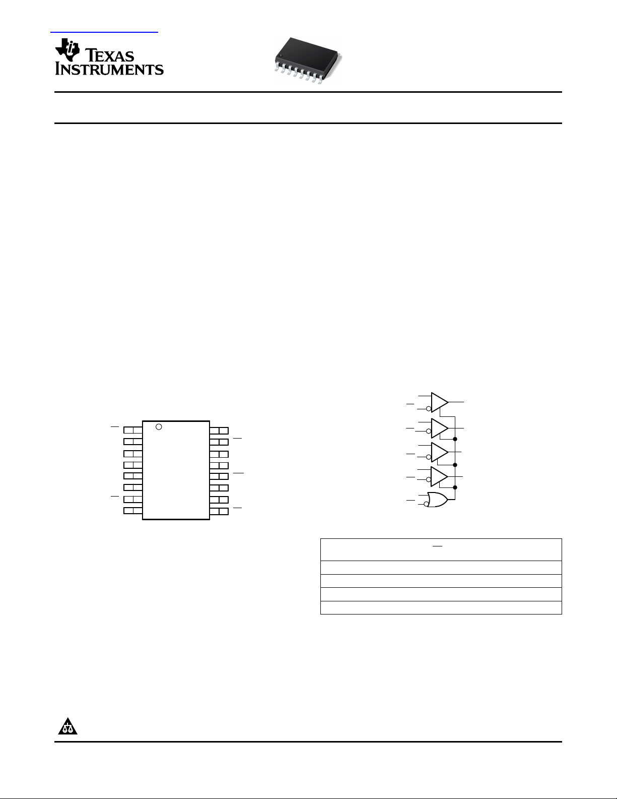
QUAD DIFFERENTIAL PECL RECEIVERS
FEATURES DESCRIPTION
• Functional Replacement for the Agere BRF1A
• Pin Equivalent to General Trade 26LS32
• High Input Impedance Approximately 8 k Ω
• <2.6-ns Maximum Propagation Delay
• TB5R3 Provides 50-mV Hysteresis (Typical)
• -1.1-V to 7.1-V Common-Mode Input Voltage
Range
• Single 5-V ± 10% Supply
• ESD Protection HBM > 3 kV and CDM > 2 kV
• Operating Temperature Range: -40 ° C to 85 ° C
• Available in Gull-Wing SOIC (JEDEC MS-013, The packaging for this differential line receiver is a
DW) and SOIC (D) Package
APPLICATIONS
• Digital Data or Clock Transmission Over Bal-
anced Lines
These quad differential receivers accept digital data
over balanced transmission lines. They translate
differential input logic levels to TTL output logic
levels.
The TB5R3 is a pin- and function-compatible replacement for the Agere systems BRF1A; it includes 3-kV
HBM and 2-kV CDM ESD protection.
The power-down loading characteristics of the receiver input circuit are approximately 8 k Ω relative to
the power supplies; hence they do not load the
transmission line when the circuit is powered down.
16-pin gull wing SOIC (DW) or a 16 pin SOIC (D).
The enable inputs of this device include internal
pull-up resistors of approximately 40 k Ω that are
connected to V
to ensure a logical high level input
CC
if the inputs are open circuited.
PIN ASSIGNMENTS
FUNCTIONAL BLOCK DIAGRAM
Enable Truth Table
E1 E2
0 0 Active
1 0 Active
0 1 Disabled
1 1 Active
OUTPUT
CONDITION
PRODUCTION DATA information is current as of publication date.
Products conform to specifications per the terms of the Texas
Instruments standard warranty. Production processing does not
necessarily include testing of all parameters.
Please be aware that an important notice concerning availability, standard warranty, and use in critical applications of Texas
Instruments semiconductor products and disclaimers thereto appears at the end of this data sheet.
Copyright © 2005, Texas Instruments Incorporated
Page 2
www.ti.com
TB5R3
SLLS643 – SEPTEMBER 2005
These devices have limited built-in ESD protection. The leads should be shorted together or the device
placed in conductive foam during storage or handling to prevent electrostatic damage to the MOS gates.
ORDERING INFORMATION
PART NUMBER
TB5R3DW TB5R3 Gull-Wing SOIC NiPdAu Production
TB5R3LDW TB5R3L Gull-Wing SOIC SnPb Production
TB5R3D TB5R3 SOIC NiPdAu Production
TB5R3LD TB5R3L SOIC SnPb Production
(1) Add the R suffix for tape and reel carrier (i.e., TB5R3DR)
POWER DISSIPATION RATINGS
PACKAGE JUNCTION-TO-AMBIENT TOR
DW
D
(1) This is the inverse of the junction-to-ambient thermal resistance when board-mounted with no air flow.
(2) In accordance with the low-K thermal metric definitions of EIA/JESD51-3.
(3) In accordance with the high-K thermal metric definitions of EIA/JESD51-7.
(1)
CIRCUIT BOARD POWER RATING POWER RATING
MODEL TA≤ 25 ° C TA= 85 ° C
Low-K
High-K
Low-K
High-K
PART MARKING Package LEAD FINISH STATUS
THERMAL RESISTANCE, DERATING FAC-
WITH NO AIR FLOW TA≥ 25 ° C
(2)
(3)
(2)
(3)
831 mW 120.3 ° C/W 8.3 mW/ ° C 332 mW
1240 mW 80.8 ° C/W 12.4 mW/ ° C 494 mW
763 mW 131.1 ° C/W 7.6 mW/ ° C 305 mW
1190 mW 84.1 ° C/W 11.9 mW/ ° C 475 mW
(1)
THERMAL CHARACTERISTICS
PARAMETER PACKAGE VALUE UNIT
θ
JB
θ
JC
Junction-to-Board
Thermal Resistance
Junction-to-Case
Thermal Resistance
DW 53.7
D 47.5
DW 47.1
D 44.2
° C/W
° C/W
ABSOLUTE MAXIMUM RATINGS
over operating free-air temperature range unless otherwise noted
Supply voltage, V
Magnitude of differential bus (input) voltage, |V
ESD
Continuous power dissipation See Dissipation Rating Table
Storage temperature, T
(1) Stresses beyond those listed under "absolute maximum ratings” may cause permanent damage to the device. These are stress ratings
only, and functional operation of the device at these or any other conditions beyond those indicated under "recommended operating
conditions” is not implied. Exposure to absolute-maximum-rated conditions for extended periods may affect device reliability.
(2) Tested in accordance with JEDEC Standard 22, Test Method A114-A.
(3) Tested in accordance with JEDEC Standard 22, Test Method C101.
CC
Human Body Model
Charged-Device Model
stg
- VAI|, |V
(2)
AI
All pins ± 3.5 kV
(3)
All pins ± 2 kV
- VBI|, |V
BI
(1)
UNIT
0 V to 6 V
- VCI|, |V
CI
- VDI| 8.4 V
DI
-65 ° C to 150 ° C
2
Page 3
www.ti.com
SLLS643 – SEPTEMBER 2005
RECOMMENDED OPERATING CONDITIONS
MIN NOM MAX UNIT
Supply voltage, V
CC
Bus pin input voltage, VAI, VAI, VBIVBI, VCI, or VCI, VDI, V
Magnitude of differential input voltage, |V
Low-level enable input voltage
High-level enable input voltage
Operating free-air temperature, T
(2)
, VIL(V
(2)
, VIH(V
A
- VAI|, |V
AI
= 5.5 V) 0.8 V
CC
= 5.5 V) 2 V
CC
DI
- VBI|, |V
BI
- VCI|, |V
CI
- VDI| 0.1 6 V
DI
4.5 5 5.5 V
(1)
-1.2
-40 85 ° C
(1) The algebraic convention, in which the least positive (most negative) limit is designated as minimum is used in this data sheet, unless
otherwise noted.
(2) The input levels and difference voltage provide no noise immunity and should be tested only in a static, noise-free environment.
DEVICE ELECTRICAL CHARACTERISTICS
over operating free-air temperature range unless otherwise noted
PARAMETER TEST CONDITIONS MIN TYP MAX UNIT
I
CC
Supply current
(1)
(1) Current is dc power draw as measured through GND pin and does not include power delivered to load.
Outputs disabled 50 mA
Outputs enabled 48 mA
TB5R3
7.2 V
RECEIVER ELECTRICAL CHARACTERISTICS
over operating free-air temperature range unless otherwise noted
PARAMETER TEST CONDITIONS MIN TYP MAX UNIT
V
V
V
V
V
V
I
I
I
I
I
I
I
R
(1) This parameter is listed using a magnitude and polarity/direction convention, rather than an algebraic convention, to match the original
(2) The input levels and difference voltage provide no noise immunity and should be tested only in a static, noise-free environment.
Output low voltage V
OL
Output high voltage V
OH
Enable input clamp voltage V
IK
Positive-going differential input threshold voltage
TH+
Negative-going differential input threshold voltage
TH-
Differential input threshold voltage hysteresis, (V
HYST
OZL
Output off-state current, (High-Z) V
OZH
Output short circuit current V
OS
Enable input low current V
IL
(2)
, (V
- VxI) x = A, B, C, or D 100 mV
xl
(2)
, (V
- VxI) x = A, B, C, or D mV
xl
- V
TH+
) 50 mV
TH_
Enable input high current VIN= 2.7 V 20 µA
IH
Enable input reverse current VIN= 5.5 V 100 µA
Differential input low current V
IL
Differential input high current VCC= 5.5V, VIN= 7.2 V 1 mA
IH
Small-signal output resistance Ω
O
= 4.5 V, IOL= 8 mA 0.4 V
CC
= 4.5 V, IOH= -400 µA 2.4 V
CC
= 4.5 V, II= -5 mA -1
CC
= 5.5 V
CC
= 5.5 V mA
CC
= 5.5 V, VIN= 0.4 V µA
CC
V
= 5.5 V
CC
= 5.5V, VIN= -1.2 V -2
CC
VO= 0.4 V -20
VO= 2.4 V 20 µA
Output High 50
Output Low 25
Agere data sheet.
(1)
V
-
(1)
100
(1)
µA
-
(1)
400
-
(1)
400
(1)
mA
3
Page 4
www.ti.com
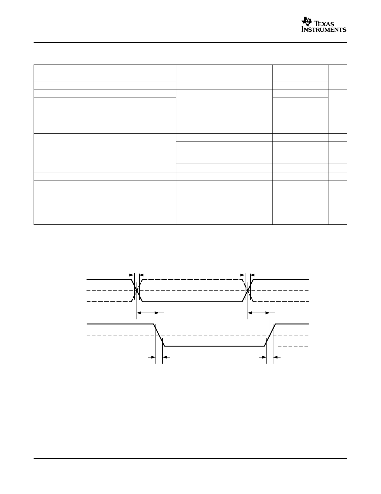
OUTPUT
3.7 V
2.7 V
3.2 V
V
OH
VOL
1.5 V
t
THL
t
PHL
t
PLH
t
TLH
20%
80%
20%
80%
INPUT
INPUT
See Note A See Note A
t
f
t
r
80% 80%
20% 20%
TB5R3
SLLS643 – SEPTEMBER 2005
SWITCHING CHARACTERISTICS
over operating free-air temperature range unless otherwise noted
PARAMETER TEST CONDITIONS MIN TYP MAX UNIT
t
PLH
t
PHL
t
PLH
t
PHL
t
PHZ
t
PLZ
t
skew1
∆ t
-p
∆ t
t
PZH
t
PZL
t
TLH
t
THL
Propagation delay time, low-to-high-level output 1.64 <2.6
Propagation delay time, high-to-low-level output 1.57 <2.6
Propagation delay time, low-to-high-level output 2.2 3.5
Propagation delay time, high-to-low-level output 2.1 3.5
Output disable time, high-level-to-high-impedance
(3)
output
Output disable time, low-level-to-high-impedance
(3)
output
Pulse-width distortion, |t
skew1p
Part-to-part output waveform skew
Same part output waveform skew CL= 10 pF, See Figure 2 and Figure 4 0.3 ns
skew
Output enable time, high-impedance-to-high-level
(3)
output
Output enable time, high-impedance-to-low-level
(3)
output
- t
PHL
|
PLH
Rise time (20%-80%) 1 ns
Fall time (80%-20%) 1 ns
CL= 0 pF
CL= 50 pF, See Figure 2 and Figure 4
(1)
, See Figure 2 and Figure 4 ns
(2)
7.7 12 ns
CL= 5 pF, See Figure 3 and Figure 5
5.2 12 ns
CL= 10 pF, See Figure 2 and Figure 4 0.7 ns
CL= 150 pF, See Figure 2 and Figure 4 4 ns
CL= 10 pF, TA= 75 ° C, See Figure 2 and
Figure 4
0.8 1.4 ns
CL= 10 pF, See Figure 2 and Figure 4 1.5 ns
6.9 12 ns
CL= 10 pF, See Figure 3 and Figure 4
6.3 12 ns
CL= 10 pF, See Figure 2 and Figure 4
ns
(1) The propagation delay values with a 0 pF load are based on design and simulation.
(2) tr/tf: 3 ns (20% - 80%)
(3) See Table 1.
A. tr/tf: 3 ns (20% - 80%)
Figure 1. Receiver Propagation Delay Times
4
Page 5

www.ti.com
OUTPUT
2.4 V
0.4 V
1.5 V
t
PHZ
t
PZH
t
PLZ
t
PZL
0.2 V
0.2 V
0.2 V
0.2 V
0.4 V
2.4 V
1.5 V
E2
See
Note A
E1
See
Note B
V
OH
V
OL
TO OUTPUT
OF DEVICE
UNDER TEST
5 V
5 k
DIODES TYPE
458E, 1N4148,
OR EQUIVALENT
2 k
C
L
CLincludes test-fixture and probe capacitance.
TO OUTPUT
OF DEVICE
UNDER TEST
C
L
500
1.5 V
CLincludes test-fixture and probe capacitance.
A. E2 = 1 while E1 changes states.
B. E1 = 0 while E2 changes states.
TB5R3
SLLS643 – SEPTEMBER 2005
Figure 2. Receiver Enable and Disable Timing
Parametric values specified under the Electrical Characteristics and Timing Characteristics sections for the data
transmission driver devices are measured with the following output load circuits.
Figure 3. Receiver Propagation Delay Time and Enable Time (t
Figure 4. Receiver Disable Time (t
, t
PHZ
) Test Circuit
PLZ
PZH
, t
) Test Circuit
PZL
5
Page 6

www.ti.com
0
2
4
3.5
3
2.5
0 50 100 150 200
t
pd
− Propagation Delay Time − ns
CL − Load Capacitance − pF
2251751257525
1.5
1
0.5
t
PLH
t
PHL
TB5R3
SLLS643 – SEPTEMBER 2005
TYPICAL CHARACTERISTICS
TYPICAL PROPAGATION DELAY
vs
LOAD CAPACITANCE
NOTE: This graph is included as an aid to the system designers. Total circuit delay varies with load capacitance. The total
delay is the sum of the delay due to external capacitance and the intrinsic delay of the device. Intrinsic delay is listed
in the table above as the 0 pF load condition. The incremental increase in delay between the 0 pF load condition and
the actual total load capacitance represents the extrinsic, or external delay contributed by the load.
Figure 5.
6
Page 7

www.ti.com
0
0.5
1
1.5
2.5
−50 0 50 100 150
− Low-to-High Propagation Delay − ns
t
PLH
T
J
− Junction Temperature − C
25−25 75 125 175
2
Max
Typ
Min
VCC = 5 V
Loaded per Figure 3
− High-to-Low Propagation Delay − ns
t
PHL
0
0.5
1
1.5
2.5
−50 0 50 100 150
T
J
− Junction Temperature − C
25−25 75 125 175
2
V
CC
= 5 V ,
Loaded per Figure 3
Typ
Min
Max
0
0.5
1
1.5
2.5
−50 0 50 100 150
T
J
− Junction Temperature − C
25−25 75 125 175
2
V
O
− Output Voltage − V
3.5
3
4
V
CC
= 4.5 V ,
Loaded per Figure 3
VOH, min
VOL, max
0
5
10
15
25
−50 0 50 100 150
T
J
− Junction Temperature − C
25−25 75 125 175
20
I
CC
− Supply Current − mA
35
30
50
V
CC
= 5.5 V
VOH, min
VOL, max
40
45
TYPICAL CHARACTERISTICS (continued)
TB5R3
SLLS643 – SEPTEMBER 2005
LOW-TO-HIGH PROPAGATION DELAY HIGH-TO-LOW PROPAGATION DELAY
vs vs
JUNCTION TEMPERATURE JUNCTION TEMPERATURE
Figure 6. Figure 7.
MINIMUM V
AND MAXIMUM V
OH
vs vs
OL
TYPICAL AND MAXIMUM I
JUNCTION TEMPERATURE JUNCTION TEMPERATURE
CC
Figure 8. Figure 9.
7
Page 8

www.ti.com
VSn I
Sn
(
VLn I
Ln
)
TJ T
A
P
D
JA
TJ T
A
P
D
JA(S)
JA(S)
JC
CA
JB
BA
JCCAJB
BA
40
60
80
100
120
140
0 100 200 300 400 500
Thermal Impedance − C/W
D, Low−K
DW, Low−K
DW, High−K
D, High−K
TB5R3
SLLS643 – SEPTEMBER 2005
APPLICATION INFORMATION
Power Dissipation
The power dissipation rating, often listed as the
package dissipation rating, is a function of the ambient temperature, TA, and the airflow around the
device. This rating correlates with the device's maximum junction temperature, sometimes listed in the
absolute maximum ratings tables. The maximum
junction temperature accounts for the processes and
materials used to fabricate and package the device,
in addition to the desired life expectancy.
There are two common approaches to estimating the
internal die junction temperature, TJ. In both of these
methods, the device internal power dissipation P
needs to be calculated This is done by totaling the
supply power(s) to arrive at the system power dissipation:
and then subtracting the total power dissipation of the
external load(s):
The first T
and ambient temperature, along with one parameter:
θJA, the junction-to-ambient thermal resistance, in
degrees Celsius per watt.
The product of P
rise above the ambient temperature. Therefore:
calculation uses the power dissipation
J
and θ
D
JA
is the junction temperature
which the device is mounted and on the airflow over
the device and PCB. JEDEC/EIA has defined
standardized test conditions for measuring θJA. Two
commonly used conditions are the low-K and the
high-K boards, covered by EIA/JESD51-3 and
EIA/JESD51-7 respectively. Figure 10 shows the
low-K and high-K values of θ
versus air flow for this
JA
device and its package options.
The standardized θ
JA
values may not accurately
represent the conditions under which the device is
used. This can be due to adjacent devices acting as
heat sources or heat sinks, to nonuniform airflow, or
to the system PCB having significantly different thermal characteristics than the standardized test PCBs.
D
The second method of system thermal analysis is
more accurate. This calculation uses the power
dissipation and ambient temperature, along with two
device and two system-level parameters:
(1)
• θJC, the junction-to-case thermal resistance, in
degrees Celsius per watt
• θJB, the junction-to-board thermal resistance, in
degrees Celsius per watt
(2)
• θCA, the case-to-ambient thermal resistance, in
degrees Celsius per watt
• θBA, the board-to-ambient thermal resistance, in
degrees Celsius per watt.
In this analysis, there are two parallel paths, one
through the case (package) to the ambient, and
another through the device to the PCB to the ambient. The system-level junction-to-ambient thermal im-
(3)
pedance, θ
, is the equivalent parallel impedance
JA(S)
of the two parallel paths:
Figure 10. Thermal Impedance vs Air Flow
Note that θ
8
is highly dependent on the PCB on
JA
where
The device parameters θ
and θ
JC
account for the
JB
internal structure of the device. The system-level
parameters θ
and θ
CA
take into account details of
BA
the PCB construction, adjacent electrical and mechanical components, and the environmental conditions
including airflow. Finite element (FE), finite difference
(FD), or computational fluid dynamics (CFD) programs can determine θ
and θBA. Details on using
CA
these programs are beyond the scope of this data
sheet, but are available from the software manufacturers.
(4)
(5)
Page 9

Page 10

Page 11

IMPORTANT NOTICE
Texas Instruments Incorporated and its subsidiaries (TI) reserve the right to make corrections, modifications,
enhancements, improvements, and other changes to its products and services at any time and to discontinue
any product or service without notice. Customers should obtain the latest relevant information before placing
orders and should verify that such information is current and complete. All products are sold subject to TI’s terms
and conditions of sale supplied at the time of order acknowledgment.
TI warrants performance of its hardware products to the specifications applicable at the time of sale in
accordance with TI’s standard warranty. Testing and other quality control techniques are used to the extent TI
deems necessary to support this warranty . Except where mandated by government requirements, testing of all
parameters of each product is not necessarily performed.
TI assumes no liability for applications assistance or customer product design. Customers are responsible for
their products and applications using TI components. To minimize the risks associated with customer products
and applications, customers should provide adequate design and operating safeguards.
TI does not warrant or represent that any license, either express or implied, is granted under any TI patent right,
copyright, mask work right, or other TI intellectual property right relating to any combination, machine, or process
in which TI products or services are used. Information published by TI regarding third-party products or services
does not constitute a license from TI to use such products or services or a warranty or endorsement thereof.
Use of such information may require a license from a third party under the patents or other intellectual property
of the third party, or a license from TI under the patents or other intellectual property of TI.
Reproduction of information in TI data books or data sheets is permissible only if reproduction is without
alteration and is accompanied by all associated warranties, conditions, limitations, and notices. Reproduction
of this information with alteration is an unfair and deceptive business practice. TI is not responsible or liable for
such altered documentation.
Resale of TI products or services with statements different from or beyond the parameters stated by TI for that
product or service voids all express and any implied warranties for the associated TI product or service and
is an unfair and deceptive business practice. TI is not responsible or liable for any such statements.
Following are URLs where you can obtain information on other Texas Instruments products and application
solutions:
Products Applications
Amplifiers amplifier.ti.com Audio www.ti.com/audio
Data Converters dataconverter.ti.com Automotive www.ti.com/automotive
DSP dsp.ti.com Broadband www.ti.com/broadband
Interface interface.ti.com Digital Control www.ti.com/digitalcontrol
Logic logic.ti.com Military www.ti.com/military
Power Mgmt power.ti.com Optical Networking www.ti.com/opticalnetwork
Microcontrollers microcontroller.ti.com Security www.ti.com/security
Telephony www.ti.com/telephony
Video & Imaging www.ti.com/video
Wireless www.ti.com/wireless
Mailing Address: Texas Instruments
Post Office Box 655303 Dallas, Texas 75265
Copyright 2005, Texas Instruments Incorporated
 Loading...