

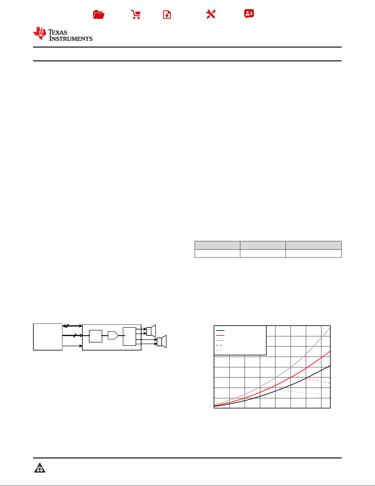
Supply Voltage (V)
Output Power (W)
5 10 15 20 24
0
20
40
60
80
10 20
D002
8 : Load Peak
6 : Load Peak
4 : Load Peak
6 : Load Continous
4 : Load Continous
System
PP
CH2
CH1
Control and
Status
Digital Audio
I2C
TAS5782M
Power
Bridge
DAC
PCDSP
Copyright © 2017, Texas Instruments Incorporated
Product
Folder
Order
Now
Technical
Documents
Tools &
Software
Support &
Community
SLASEG8A –MARCH 2016–REVISED JULY 2017
TAS5782M 30 W Stereo Class-D Amplifier with 96-kHz Processing
TAS5782M
1 Features
1
• Flexible Audio I/O Configuration
– Supports I2S, TDM, LJ, RJ Digital Input
– Sample Rate Support
– BD Amplifier Modulation
– Supports 3-Wire Digital Audio Interface (No
MCLK required)
• High-Performance Closed-Loop Architecture
(PVDD = 12 V, R
– Closed-Loop = reduced component count/
smaller solution size
– Idle Channel Noise = 62 µVrms (A-Wtd)
– THD+N = 0.2% (at 1 W, 1 kHz)
– SNR = 103dB A-Wtd (Ref. to THD+N = 1%)
• Flexible Processing Features
– 15 BiQuads / SmartEQ
– 2 x 5 BiQuads for X-Over / EQ
– 3-Band Advanced DRC + AGL
– Dynamic EQ and SmartBass
– Sound Field Spatializer (SFS)
– 96-kHz Processor Sampling
• Communication Features
– Software Mode Control via I2C Port
– Two Address Select Pins – Up to 4 Devices
• Robustness and Reliability Features
– Clock Error , DC, and Short-Circuit Protection
– Overtemperature and Overcurrent Protection
SPACE
Simplified Block Diagram
= 8 Ω, SPK_GAIN = 20 dB)
SPK
2 Applications
• LCD, LED TV, and Multi-Purpose Monitors
• Sound Bars, Docking Stations, and PC Audio
• Wireless Subwoofers, Bluetooth Speakers, and
Active Speakers
3 Description
The TAS5782M device is a high-performance, stereo
closed-loop Class-D amplifier with integrated audio
processor with up to 96-kHz architecture. To convert
from digital to analog, the device uses a high
performance DAC with Burr Brown™ audio
technology. It requires only two power supplies: one
DVDD for low-voltage circuitry and one PVDD for
high-voltage circuitry. It is controlled by a software
control port using standard I2C communication.
An optimal mix of thermal performance and device
cost is provided in the 90 mΩ r
MOSFETs. Additionally, a thermally enhanced 48-Pin
TSSOP provides excellent operation in the elevated
ambient temperatures found in modern consumer
electronic devices.
Device Information
PART NUMBER PACKAGE BODY SIZE (NOM)
TAS5782M TSSOP (48) 12.50 mm × 6.10 mm
(1) For all available packages, see the orderable addendum at
the end of the data sheet.
Power at 10% THD+N vs PVDD
DS(on)
(1)
of the output
(1)
1
An IMPORTANT NOTICE at the end of this data sheet addresses availability, warranty, changes, use in safety-critical applications,
intellectual property matters and other important disclaimers. PRODUCTION DATA.
(1) Tested on TAS5782MEVM Board.

TAS5782M
SLASEG8A –MARCH 2016–REVISED JULY 2017
www.ti.com
Table of Contents
1 Features.................................................................. 1
2 Applications ........................................................... 1
3 Description ............................................................. 1
4 Revision History..................................................... 2
5 Device Comparison Table..................................... 3
6 Pin Configuration and Functions......................... 4
6.1 Internal Pin Configurations........................................ 6
7 Specifications......................................................... 9
7.1 Absolute Maximum Ratings ...................................... 9
7.2 ESD Ratings.............................................................. 9
7.3 Recommended Operating Conditions..................... 10
7.4 Thermal Information................................................ 10
7.5 Electrical Characteristics......................................... 11
7.6 Power Dissipation Characteristics .......................... 15
7.7 MCLK Timing ......................................................... 20
7.8 Serial Audio Port Timing – Slave Mode.................. 20
7.9 Serial Audio Port Timing – Master Mode................ 21
7.10 I2C Bus Timing – Standard................................... 21
7.11 I2C Bus Timing – Fast........................................... 21
7.12 SPK_MUTE Timing .............................................. 22
7.13 Typical Characteristics.......................................... 24
8 Parametric Measurement Information ............... 33
9 Detailed Description............................................ 34
9.1 Overview................................................................. 34
9.2 Functional Block Diagram ....................................... 34
9.3 Feature Description................................................. 35
9.4 Device Functional Modes........................................ 56
10 Application and Implementation........................ 59
10.1 Application Information.......................................... 59
10.2 Typical Applications ............................................. 61
11 Power Supply Recommendations ..................... 70
11.1 Power Supplies ..................................................... 70
12 Layout................................................................... 72
12.1 Layout Guidelines ................................................. 72
12.2 Layout Example .................................................... 74
13 Register Maps...................................................... 80
13.1 Registers - Page 0 ................................................ 80
13.2 Registers - Page 1 .............................................. 116
14 Device and Documentation Support ............... 120
14.1 Device Support.................................................... 120
14.2 Receiving Notification of Documentation
Updates.................................................................. 120
14.3 Community Resources........................................ 121
14.4 Trademarks......................................................... 121
14.5 Electrostatic Discharge Caution.......................... 121
14.6 Glossary.............................................................. 121
15 Mechanical, Packaging, and Orderable
Information......................................................... 121
4 Revision History
NOTE: Page numbers for previous revisions may differ from page numbers in the current version.
Changes from Original (March 2017) to Revision A Page
• Added missing cross references to the Quick Reference Table .......................................................................................... 24
• Changed Changed the Volume Ramp Up/Down Step default value to 11 .......................................................................... 50
• Changed 5th bit of the I2C Slave Address table .................................................................................................................. 54
• Added DSP Book, Page, and Register Update section ....................................................................................................... 56
• Deleted Page 0 Registers 0x0A, 0x50, 0x51, 0x52, and 0x54............................................................................................. 80
• Changed the PLLE bit type of Register 4 from R to R/W..................................................................................................... 81
• Changed Bit configuration of Register 0x14......................................................................................................................... 88
• Changed PJDV bit in Register 21 from 5-4 to 5-0................................................................................................................ 89
• Changed Reset value of Register 0x3D to '00110000'......................................................................................................... 98
• Changed Bit configuration of Register 0x5D ...................................................................................................................... 112
• Deleted Page 1 Registers 0x05 and 0x08.......................................................................................................................... 116
2
Submit Documentation Feedback Copyright © 2016–2017, Texas Instruments Incorporated
Product Folder Links: TAS5782M
www.ti.com
5 Device Comparison Table
DEVICE NAME MODULATION STYLE PROCESSING TYPE
TAS5782MDCA BD Modulation
TAS5754MDCA 1SPW (Ternary)
TAS5756MDCA BD Modulation
TAS5766MDCA BD Modulation 50 MIPs, Fixed-Function (Uses single ROM image of process flow)
TAS5782M
SLASEG8A –MARCH 2016–REVISED JULY 2017
100 MIPs, Flexible Process flow (Uses mixture of RAM and ROM
components to create several process flows)
50 MIPs, HybridFlow (Uses mixture of RAM and ROM components to
create several process flows)
50 MIPs, HybridFlow (Uses mixture of RAM and ROM components to
create several process flows)
Product Folder Links: TAS5782M
Submit Documentation FeedbackCopyright © 2016–2017, Texas Instruments Incorporated
3
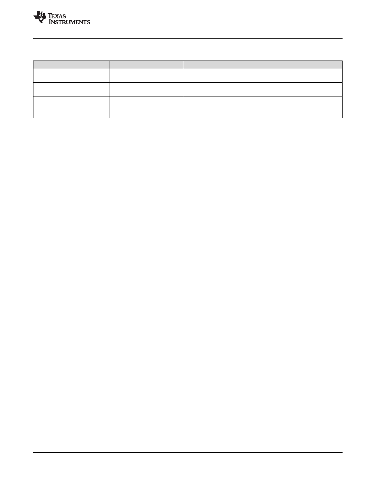
1
5
4
3
2
6
10
9
8
7
12
11
36
32
33
34
35
31
27
28
29
30
25
26
PowerPAD
TM
SPK_OUTA-
PGND
SPK_OUTA+
PVDD
SPK_GAIN/FSW
BSTRPA+
SPK_INA-
DVDD_REG
CN
GND
CPVSS
CP
SPK_OUTB+
CPVDD
DVDD
LRCLK/FS
DGND
ADR0
SPK_MUTE
14
13
16
15
18
17
20
19
22
21
24
23
48
44
45
46
47
43
39
40
41
42
37
38
PVDD
SPK_OUTB-
PGND
BSTRPB-
BSTRPB+
PVDD
SPK_FAULT
SPK_INB-
PVDD
SPK_INB+
DAC_OUTB
PGND
SPK_INA+
DAC_OUTA
AGND
SCL
RESET
ADR1
GPIO0
GPIO2
BSTRPA-
SDA
SCLK
SDIN
PVDD
AGND
AVDD
GVDD_REG
MCLK
TAS5782M
SLASEG8A –MARCH 2016–REVISED JULY 2017
6 Pin Configuration and Functions
www.ti.com
48-Pin TSSOP with PowerPAD™
DCA Package
Top View
4
Submit Documentation Feedback Copyright © 2016–2017, Texas Instruments Incorporated
Product Folder Links: TAS5782M

www.ti.com
SLASEG8A –MARCH 2016–REVISED JULY 2017
Pin Functions
PIN
NAME NO.
ADR0 26 DI
ADR1 20 DI
AGND
AVDD 14 P Figure 2 Power supply for internal analog circuitry
BSTRPA– 1 P
BSTRPA+ 5 P
BSTRPB– 48 P
BSTRPB+ 44 P
CN 34 P Figure 14 Negative pin for capacitor connection used in the line-driver charge pump
CP 32 P Figure 13 Positive pin for capacitor connection used in the line-driver charge pump
CPVDD 31 P Figure 2 Power supply for charge pump circuitry
CPVSS 35 P Figure 14 –3.3-V supply generated by charge pump for the DAC
DAC_OUTA 13 AO
DAC_OUTB 36 AO Single-ended output for Channel B of the DAC
DGND 29 G — Ground reference for digital circuitry. Connect this pin to the system ground.
DVDD 30 P Figure 2 Power supply for the internal digital circuitry
DVDD_REG 28 P Figure 15
GND 33 G — Ground pin for device. This pin should be connected to the system ground.
GPIO0 18
GPIO2 21
GVDD_REG 8 P Figure 5
LRCK/FS 25 DI/O
MCLK 22 DI Master clock used for internal clock tree and sub-circuit and state machine clocking
PGND
PVDD
RESET 19 DI Figure 17 Device reset input. Pull down to reset, pull up to activate device.
SCL 17 DI Figure 10
SCLK 23 DI/O Figure 11 Bit clock for the digital signal that is active on the input data line of the serial data port
SDA 16 DI/O Figure 9
SDIN 24 D1 Figure 11 Data line to the serial data port
SPK_INA– 11 AI
SPK_INA+ 12 AI Positive pin for differential speaker amplifier input A
SPK_INB– 38 AI Negative pin for differential speaker amplifier input B
SPK_INB+ 37 AI Positive pin for differential speaker amplifier input B
TYPE
10
15
3
46
6
7
41
42
43
G — Ground reference for analog circuitry
DI/O General purpose input/output pins (GPIOx). Refer to GPIO registers for configuration.
G — Ground reference for power device circuitry. Connect this pin to the system ground.39
P Figure 1 Power supply for internal power circuitry
(1)
TERMINATION
INTERNAL
Figure 3
Figure 8
Figure 11
Figure 7
DESCRIPTION
Sets the LSB of the I2C address to 0 if pulled to GND, to 1 if pulled to DVDD
Sets the second LSB of the I2C address to 0 if pulled to GND, to 1 if pulled to DVDD
(2)
Connection point for the SPK_OUTA– bootstrap capacitor which is used to create a power supply for
the high-side gate drive for SPK_OUTA–
Connection point for the SPK_OUTA+ bootstrap capacitor which is used to create a power supply for
the high-side gate drive for SPK_OUTA+
Connection point for the SPK_OUTB– bootstrap capacitor which is used to create a power supply for
the high-side gate drive for SPK_OUTB–
Connection point for the SPK_OUTB+ bootstrap capacitor which is used to create a power supply for
the high-side gate drive for SPK_OUTB+
Single-ended output for Channel A of the DAC
Voltage regulator derived from DVDD supply for use for internal digital circuitry. This pin is provided
as a connection point for filtering capacitors for this supply and must not be used to power any
external circuitry.
Voltage regulator derived from PVDD supply to generate the voltage required for the gate drive of
output MOSFETs. This pin is provided as a connection point for filtering capacitors for this supply and
must not be used to power any external circuitry.
Word select clock for the digital signal that is active on the serial port's input data line. In I2S, LJ, and
RJ, this corresponds to the left channel and right channel boundary. In TDM mode, this corresponds
to the frame sync boundary.
I2C serial control port clock
I2C serial control port data
Negative pin for differential speaker amplifier input A
TAS5782M
(1) AI = Analog input, AO = Analog output, DI = Digital Input, DO = Digital Output, DI/O = Digital Bi-directional (input and output), P =
Power, G = Ground (0 V)
(2) This pin should be connected to the system ground.
Submit Documentation FeedbackCopyright © 2016–2017, Texas Instruments Incorporated
Product Folder Links: TAS5782M
5

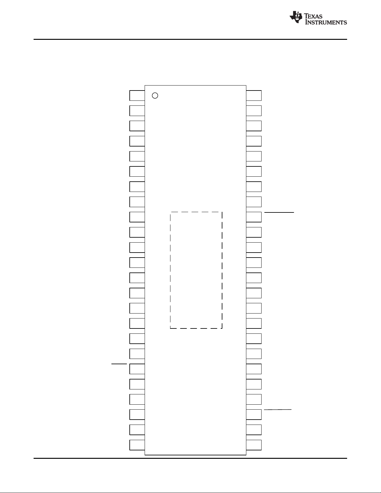
PVDD
SPK_OUTxx
Copyright © 2016, Texas Instruments Incorporated
GVDD
PVDD
SPK_OUTxx
BSTRPxx
7 V ESD
Copyright © 2016, Texas Instruments Incorporated
PVDD
30 V ESD
Copyright © 2016, Texas Instruments Incorporated
DVDD
3.3 V ESD
Copyright © 2016, Texas Instruments Incorporated
TAS5782M
SLASEG8A –MARCH 2016–REVISED JULY 2017
Pin Functions (continued)
PIN
NAME NO.
SPK_FAULT 40 DO Figure 16 Fault pin which is pulled low when an overcurrent, overtemperature, or DC detect fault occurs
SPK_GAIN/F
REQ
SPK_OUTA– 2 AO
SPK_OUTA+ 4 AO Positive pin for differential speaker amplifier output A
SPK_OUTB– 47 AO Negative pin for differential speaker amplifier output B
SPK_OUTB+ 45 AO Positive pin for differential speaker amplifier output B
SPK_MUTE 27 I Figure 12
PowerPAD — G —
TYPE
9 AI Figure 6 Sets the gain and switching frequency of the speaker amplifier, latched in upon start-up of the device.
(1)
TERMINATION
INTERNAL
Figure 4
DESCRIPTION
Negative pin for differential speaker amplifier output A
Speaker amplifier mute which must be pulled low (connected to DGND) to mute the device and
pulled high (connected to DVDD) to unmute the device.
Provides both electrical and thermal connection from the device to the board. A matching ground pad
must be provided on the PCB and the device connected to it through solder. For proper electrical
operation, this ground pad must be connected to the system ground.
6.1 Internal Pin Configurations
www.ti.com
Figure 1. PVDD Pins Figure 2. AVDD, DVDD and CPVDD Pins
Figure 3. BSTRPxx Pins Figure 4. SPK_OUTxx Pins
6
Submit Documentation Feedback Copyright © 2016–2017, Texas Instruments Incorporated
Product Folder Links: TAS5782M
SDA
3.3 V
ESD
DVDD
Copyright © 2016, Texas Instruments Incorporated
SCL
3.3 V
ESD
DVDD
Copyright © 2016, Texas Instruments Incorporated
SPK_INxx
7 V ESD
Gain Switch
Copyright © 2016, Texas Instruments Incorporated
AVDD
CPVSS
DAC_OUTA
Copyright © 2016, Texas Instruments Incorporated
GVDD
7 V ESD
PVDD
10 Ÿ
Copyright © 2016, Texas Instruments Incorporated
GVDD
SPK_GAIN/FREQ
7 V ESD
10 NŸ
Copyright © 2016, Texas Instruments Incorporated
www.ti.com
Internal Pin Configurations (continued)
Figure 5. GVDD_REG Pin Figure 6. SPK_GAIN/FREQ Pin
TAS5782M
SLASEG8A –MARCH 2016–REVISED JULY 2017
Figure 7. SPK_INxx Pins Figure 8. DAC_OUTx Pins
Figure 9. SDA Pin Figure 10. SCL Pin
Submit Documentation FeedbackCopyright © 2016–2017, Texas Instruments Incorporated
Product Folder Links: TAS5782M
7
DVDD
1.8 V
ESD
DVDD_REG
Copyright © 2016, Texas Instruments Incorporated
28 V
ESD
SPK_FAULT
100 Ÿ
Copyright © 2016, Texas Instruments Incorporated
CVPDD
3.3 V
ESD
CP
Copyright © 2016, Texas Instruments Incorporated
CN
3.3 V
ESD
CPVSS
3.3 V
ESD
GND
Copyright © 2016, Texas Instruments Incorporated
DVDD
3.3 V
ESD
MCLK
SCLK
SDIN
LRCK/FS
Copyright © 2016, Texas Instruments Incorporated
DVDD
3.3 V
ESD
SPK_MUTE
Copyright © 2016, Texas Instruments Incorporated
TAS5782M
SLASEG8A –MARCH 2016–REVISED JULY 2017
Internal Pin Configurations (continued)
Figure 11. SCLK, MCLK, SDIN, and LRCK/FS Pins Figure 12. SPK_MUTE Pin
www.ti.com
8
Figure 13. CP Pin Figure 14. CN and CPVSS Pins
Submit Documentation Feedback Copyright © 2016–2017, Texas Instruments Incorporated
Figure 15. DVDD_REG Pin Figure 16. SPK_FAULT Pin
Product Folder Links: TAS5782M
RESET
3.3 V
ESD
DVDD
Copyright © 2016, Texas Instruments Incorporated
TAS5782M
www.ti.com
SLASEG8A –MARCH 2016–REVISED JULY 2017
Internal Pin Configurations (continued)
Figure 17. RESET Pin
7 Specifications
7.1 Absolute Maximum Ratings
Free-air room temperature 25°C (unless otherwise noted)
DVDD, AVDD,
CPVDD
PVDD PVDD supply –0.3 30 V
V
I(AmpCtrl)
V
I(DigIn)
V
I(SPK_INxx)
V
I(SPK_OUTxx)
T
J
T
stg
(1) Stresses beyond those listed under Absolute Maximum Ratings may cause permanent damage to the device. These are stress ratings
only, and functional operation of the device at these or any other conditions beyond those indicated under Recommended Operating
Conditions is not implied. Exposure to absolute-maximum-rated conditions for extended periods may affect device reliability.
(2) DVDD referenced digital pins include: ADR0, ADR1, GPIO0, GPIO2, LRCK/FS, MCLK, RESET, SCL, SCLK, SDA, SDIN, and
SPK_MUTE.
Low-voltage digital, analog, charge pump supply –0.3 3.9 V
Input voltage for SPK_GAIN/FREQ and SPK_FAULT pins –0.3 V
DVDD referenced digital inputs
(2)
Analog input into speaker amplifier –0.3 6.3 V
Voltage at speaker output pins –0.3 32 V
Ambient operating temperature, T
A
Operating junction temperature, digital die –40 125 °C
Operating junction temperature, power die –40 165 °C
Storage temperature –40 125 °C
(1)
MIN MAX UNIT
+ 0.3 V
GVDD
–0.5 V
+ 0.5 V
DVDD
–25 85 °C
7.2 ESD Ratings
VALUE UNIT
V
(ESD)
Electrostatic
discharge
Human-body model (HBM), per ANSI/ESDA/JEDEC JS-001
Charged-device model (CDM), per JEDEC specification JESD22-C101
(1) JEDEC document JEP155 states that 2000-V HBM allows safe manufacturing with a standard ESD control process.
(2) JEDEC document JEP157 states that 500-V CDM allows safe manufacturing with a standard ESD control process.
Product Folder Links: TAS5782M
(1)
(2)
±2000
±500
Submit Documentation FeedbackCopyright © 2016–2017, Texas Instruments Incorporated
V
9
TAS5782M
SLASEG8A –MARCH 2016–REVISED JULY 2017
www.ti.com
7.3 Recommended Operating Conditions
Free-air room temperature 25°C (unless otherwise noted)
MIN NOM MAX UNIT
V
(POWER)
R
SPK
V
IH(DigIn)
V
IL(DigIn)
L
OUT
Power supply inputs
Minimum speaker load
Input logic high for DVDD referenced digital inputs
Input logic low for DVDD referenced digital inputs
Minimum inductor value in LC filter under short-circuit
condition
(1) DVDD referenced digital pins include: ADR0, ADR1, GPIO0, GPIO2, LRCK/FS, MCLK, RESET, SCL, SCLK, SDA, SDIN, and
SPK_MUTE.
(2) The best practice for driving the input pins of the TAS5782M device is to power the drive circuit or pullup resistor from the same supply
which provides the DVDD power supply.
(3) The best practice for driving the input pins of the TAS5782M device low is to pull them down, either actively or through pulldown
resistors to the system ground.
DVDD, AVDD, CPVDD 2.9 3.63
PVDD 4.5 26.4
BTL Mode 3 Ω
PBTL Mode 2 Ω
(1)(2)
(1)(3)
0.9 × V
V
DVDD
DVDD
0 0.1 × V
V
DVDD
DVDD
1 4.7 µH
V
V
V
7.4 Thermal Information
TAS5782M
DCA (TSSOP)
THERMAL METRIC
(1)
JEDEC
STANDARD
2-LAYER PCB
R
θJA
R
θJC(top)
R
θJB
ψ
JT
ψ
JB
R
θJC(bot)
Junction-to-ambient thermal resistance 41.8 27.6 19.4 °C/W
Junction-to-case (top) thermal resistance 14.4 14.4 14.4 °C/W
Junction-to-board thermal resistance 9.4 9.4 9.4 °C/W
Junction-to-top characterization parameter 0.6 0.6 2 °C/W
Junction-to-board characterization parameter 8.1 9.3 4.8 °C/W
Junction-to-case (bottom) thermal resistance N/A N/A N/A °C/W
(1) For more information about traditional and new thermal metrics, see the Semiconductor and IC Package Thermal Metrics application
report.
48 PINS
JEDEC
STANDARD
4-LAYER PCB
UNIT
TAS5782MEVM
4-LAYER PCB
10
Submit Documentation Feedback Copyright © 2016–2017, Texas Instruments Incorporated
Product Folder Links: TAS5782M
TAS5782M
www.ti.com
SLASEG8A –MARCH 2016–REVISED JULY 2017
7.5 Electrical Characteristics
Free-air room temperature 25°C (unless otherwise noted) Measurements were made using TAS5782MEVM board and Audio
Precision System 2722 with Analog Analyzer filter set to 40 kHz brickwall filter. The device output PWM frequency was set to
768 kHz unless otherwise noted.
PARAMETER TEST CONDITIONS MIN TYP MAX UNIT
DIGITAL I/O
|IIH|1
|IIL|1
V
IH1
V
IL1
V
OH(DigOut)
V
OL(DigOut)
V
OL(SPK_FAULT)
GVDD_REG GVDD regulator voltage 7 V
I2C CONTROL PORT
C
L(I2C)
f
SCL(fast)
f
SCL(slow)
V
NH
MCLK AND PLL SPECIFICATIONS
D
MCLK
f
MCLK
f
PLL
SERIAL AUDIO PORT
t
DLY
D
SCLK
f
S
f
SCLK
f
SCLK
SPEAKER AMPLIFIER (ALL OUTPUT CONFIGURATIONS)
A
V(SPK_AMP)
ΔA
V(SPK_AMP)
Input logic high current level
for DVDD referenced digital
input pins
(1)
V
IN(DigIn)
= V
DVDD
10 µA
Input logic low current level
for DVDD referenced digital
input pins
(1)
V
= 0 V –10 µA
IN(DigIn)
Input logic high threshold for
DVDD referenced digital
(1)
inputs
70% V
DVDD
Input logic low threshold for
DVDD referenced digital
(1)
inputs
Output logic high voltage
(1)
level
Output logic low voltage
(1)
level
Output logic low voltage level
for SPK_FAULT
Allowable load capacitance
for each I2C Line
IOH= 4 mA 80% V
IOH= –4 mA 22% V
With 100-kΩ pullup resistor 0.8 V
30% V
400 pF
DVDD
DVDD
DVDD
Support SCL frequency No wait states, fast mode 400 kHz
Support SCL frequency No wait states, slow mode 100 kHz
Noise margin at High level for
each connected device
(including hysteresis)
0.2 × V
DD
V
Allowable MCLK duty cycle 40% 60%
Supported MCLK frequencies Up to 50 MHz 128 512 f
PLL input frequency
Required LRCK/FS to SCLK
rising edge delay
Clock divider uses fractional divide
D > 0, P = 1
Clock divider uses integer divide
D = 0, P = 1
6.7 20
1 20
5 ns
S
MHz
Allowable SCLK duty cycle 40% 60%
Supported input sample rates 8 96 kHz
Supported SCLK frequencies 32 64 f
S
SCLK frequency Either master mode or slave mode 24.576 MHz
SPK_GAIN/FREQ voltage < 3 V,
Speaker amplifier gain
see Adjustable Amplifier Gain and Switching
Frequency Selection
SPK_GAIN/FREQ voltage > 3.3 V,
see Adjustable Amplifier Gain and Switching
20
dBV
26
Frequency Selection
Typical variation of speaker
amplifier gain
±1 dBV
(2)
(2)
(1) DVDD referenced digital pins include: ADR0, ADR1, GPIO0, GPIO2, LRCK/FS, MCLK,RESET, SCL, SCLK, SDA, SDIN, and
SPK_MUTE.
(2) A unit of fSindicates that the specification is the value listed in the table multiplied by the sample rate of the audio used in the
TAS5782M device.
Submit Documentation FeedbackCopyright © 2016–2017, Texas Instruments Incorporated
Product Folder Links: TAS5782M
11
TAS5782M
SLASEG8A –MARCH 2016–REVISED JULY 2017
www.ti.com
Electrical Characteristics (continued)
Free-air room temperature 25°C (unless otherwise noted) Measurements were made using TAS5782MEVM board and Audio
Precision System 2722 with Analog Analyzer filter set to 40 kHz brickwall filter. The device output PWM frequency was set to
768 kHz unless otherwise noted.
PARAMETER TEST CONDITIONS MIN TYP MAX UNIT
Switching frequency depends on voltage
f
SPK_AMP
K
SVR
Switching frequency of the
speaker amplifier
Power supply rejection ratio
Drain-to-source on resistance
r
DS(on)
OCE
OTE
THRES
THRES
of the individual output
MOSFETs
SPK_OUTxx overcurrent
error threshold
Overtemperature error
threshold
Time required to clear
OCE
CLRTIME
overcurrent error after error
condition is removed.
Time required to clear
OTE
OVE
UVE
CLRTIME
THRES(PVDD)
THRES(PVDD)
overtemperature error after
error condition is removed.
PVDD overvoltage error
threshold
PVDD undervoltage error
threshold
SPEAKER AMPLIFIER (STEREO BTL)
|VOS| Amplifier offset voltage
I
CN(SPK)
P
O(SPK)
Idle channel noise
Output Power (Per Channel)
presented at SPK_GAIN/FREQ pin and the
clocking arrangement, including the incoming
sample rate, see Adjustable Amplifier Gain and
Switching Frequency Selection
Injected Noise = 50 Hz to 60 Hz, 200 mV
= 26 dB, input audio signal = digital zero
V
= 24 V, I
PVDD
includes PVDD/PGND pins, leadframe, bondwires
= 500 mA, TJ= 25°C,
(SPK_OUT)
P-P
, Gain
and metallization layers.
V
PVDD
= 24 V, I
= 500 mA, TJ= 25°C 90
(SPK_OUT)
Measured differentially with zero input data,
SPK_GAIN/FREQ pin configured for 20 dB gain,
V
= 12 V
PVDD
Measured differentially with zero input data,
SPK_GAIN/FREQ pin configured for 26 dB gain,
V
= 24 V
PVDD
V
= 12 V, SPK_GAIN = 20 dB, R
PVDD
Weighted
V
= 15 V, SPK_GAIN = 20 dB, R
PVDD
Weighted
V
= 19 V, SPK_GAIN = 26 dB, R
PVDD
Weighted
V
= 24 V, SPK_GAIN = 26 dB, R
PVDD
Weighted
V
= 12 V, SPK_GAIN = 20 dB, R
PVDD
THD+N = 0.1%
V
= 12 V, SPK_GAIN = 20 dB, R
PVDD
THD+N = 0.1%
V
= 15 V, SPK_GAIN = 26 dB, R
PVDD
THD+N = 0.1%
V
= 15 V, SPK_GAIN = 26 dB, R
PVDD
THD+N = 0.1%
V
= 19 V, SPK_GAIN = 26 dB, R
PVDD
THD+N = 0.1%
V
= 19 V, SPK_GAIN = 26 dB, R
PVDD
THD+N = 0.1%
V
= 24 V, SPK_GAIN = 26 dB, R
PVDD
THD+N = 0.1%
V
= 24 V, SPK_GAIN = 26 dB, R
PVDD
THD+N = 0.1%
SPK
SPK
SPK
SPK
SPK
SPK
SPK
SPK
SPK
SPK
SPK
SPK
= 8 Ω, A-
= 8 Ω, A-
= 8 Ω, A-
= 8 Ω, A-
= 4 Ω,
= 8 Ω,
= 4 Ω,
= 8 Ω,
= 4 Ω,
= 8 Ω,
= 4 Ω,
= 8 Ω,
176.4 768 kHz
60 dB
120
mΩ
7.5 A
165 °C
1.3 s
1.3 s
27 V
4.3 V
2
mV
5 15
49
59
µV
81
82
14
8
23
13
W
34
20
40
33
RMS
12
Submit Documentation Feedback Copyright © 2016–2017, Texas Instruments Incorporated
Product Folder Links: TAS5782M
TAS5782M
www.ti.com
SLASEG8A –MARCH 2016–REVISED JULY 2017
Electrical Characteristics (continued)
Free-air room temperature 25°C (unless otherwise noted) Measurements were made using TAS5782MEVM board and Audio
Precision System 2722 with Analog Analyzer filter set to 40 kHz brickwall filter. The device output PWM frequency was set to
768 kHz unless otherwise noted.
PARAMETER TEST CONDITIONS MIN TYP MAX UNIT
V
SNR
(referenced to 0 dBFS input
signal)
Signal-to-noise ratio
THD+N
SPK
Total harmonic distortion and
noise
Cross-talk (worst case
X-talk
SPK
between left-to-right and
right-to-left coupling)
SPEAKER AMPLIFIER (MONO PBTL)
|VOS| Amplifier offset voltage
I
CN
Idle channel noise
= 12 V, SPK_GAIN = 20 dB, R
PVDD
Weighted, –120 dBFS Input
V
= 15 V, SPK_GAIN = 26 dB, R
PVDD
Weighted, –120 dBFS Input
V
= 19 V, SPK_GAIN = 26 dB, R
PVDD
Weighted, –120 dBFS Input
V
= 24 V, SPK_GAIN = 26 dB, R
PVDD
Weighted, –120 dBFS Input
V
= 12 V, SPK_GAIN = 20 dB, R
PVDD
PO= 1 W, f = 1kHz
V
= 12 V, SPK_GAIN = 20 dB, R
PVDD
PO= 1 W, f = 1kHz
V
= 15 V, SPK_GAIN = 26 dB, R
PVDD
PO= 1 W, f = 1kHz
V
= 15 V, SPK_GAIN = 26 dB, R
PVDD
PO= 1 W, f = 1kHz
V
= 19 V, SPK_GAIN = 26 dB, R
PVDD
PO= 1 W, f = 1kHz
V
= 19 V, SPK_GAIN = 26 dB, R
PVDD
PO= 1 W, f = 1kHz
V
= 24 V, SPK_GAIN = 26 dB, R
PVDD
PO= 1 W, f = 1kHz
V
= 24 V, SPK_GAIN = 26 dB, R
PVDD
PO= 1 W, f = 1kHz
V
= 12 V, SPK_GAIN = 20 dB, R
PVDD
Input Signal 250 mVrms,
1-kHz Sine, across f(S)
V
= 15 V, SPK_GAIN = 26 dBV, R
PVDD
Input Signal 250 mVrms,
1-kHz Sine, across f(S)
V
= 19 V, SPK_GAIN = 26 dBV, R
PVDD
Input Signal 250 mVrms,
1-kHz Sine, across f(S)
V
= 24 V, SPK_GAIN = 26 dBV, R
PVDD
Input Signal 250 mVrms,
1-kHz Sine, across f(S)
Measured differentially with zero input data,
SPK_GAIN/FREQ pin configured for 20 dB gain,
V
= 12 V
PVDD
Measured differentially with zero input data,
SPK_GAIN/FREQ pin configured for 26 dB gain,
V
= 24 V
PVDD
V
= 12 V, SPK_GAIN = 20 dB, R
PVDD
Weighted
V
= 15 V, SPK_GAIN = 20 dB, RSPK = 8 Ω,
PVDD
A-Weighted
V
= 19 V, SPK_GAIN = 26 dB, RSPK = 8 Ω,
PVDD
A-Weighted
V
= 24 V, SPK_GAIN = 26 dB, R
PVDD
Weighted
SPK
SPK
SPK
SPK
SPK
SPK
SPK
SPK
SPK
SPK
SPK
SPK
SPK
SPK
SPK
SPK
SPK
SPK
= 8 Ω, A-
= 8 Ω, A-
= 8 Ω, A-
= 8 Ω, A-
= 4 Ω,
= 8 Ω,
= 4 Ω,
= 8 Ω,
= 4 Ω,
= 8 Ω,
= 4 Ω,
= 8 Ω,
= 8 Ω,
= 8 Ω,
= 8 Ω,
= 8 Ω,
= 8 Ω, A-
= 8 Ω, A-
103
102
103
105
0.021%
0.022%
0.02%
0.037%
0021%
0.028%
0.027%
0.038%
–90
–102
–93
–93
0.7
48
49
83
82
dB
dB
mV
4
µV
RMS
Product Folder Links: TAS5782M
Submit Documentation FeedbackCopyright © 2016–2017, Texas Instruments Incorporated
13

TAS5782M
SLASEG8A –MARCH 2016–REVISED JULY 2017
www.ti.com
Electrical Characteristics (continued)
Free-air room temperature 25°C (unless otherwise noted) Measurements were made using TAS5782MEVM board and Audio
Precision System 2722 with Analog Analyzer filter set to 40 kHz brickwall filter. The device output PWM frequency was set to
768 kHz unless otherwise noted.
PARAMETER TEST CONDITIONS MIN TYP MAX UNIT
V
P
O
SNR
THD+N
Output power (per channel)
Signal-to-noise ratio
(referenced to 0 dBFS input
signal)
Total harmonic distortion and
noise
= 12 V, SPK_GAIN = 20 dB, R
PVDD
THD+N = 0.1%, Unless otherwise noted
V
= 12 V, SPK_GAIN = 20 dB, R
PVDD
THD+N = 0.1%, Unless otherwise noted
V
= 12 V, SPK_GAIN = 20 dB, R
PVDD
THD+N = 0.1%
V
= 15 V, SPK_GAIN = 26 dB, R
PVDD
THD+N = 0.1%, Unless otherwise noted
V
= 15 V, SPK_GAIN = 26 dB, R
PVDD
THD+N = 0.1%, Unless otherwise noted
V
= 15 V, SPK_GAIN = 26 dB, R
PVDD
THD+N = 0.1%
V
= 19 V, SPK_GAIN = 26 dB, R
PVDD
THD+N = 0.1%, Unless otherwise noted
V
= 19 V, SPK_GAIN = 26 dB, R
PVDD
THD+N = 0.1%, Unless otherwise noted
V
= 19 V, SPK_GAIN = 26 dB, R
PVDD
THD+N = 0.1%
V
= 24 V, SPK_GAIN = 26 dB, R
PVDD
THD+N = 0.1%, Unless otherwise noted
V
= 24 V, SPK_GAIN = 26 dB, R
PVDD
THD+N = 0.1%, Unless otherwise noted
V
= 24 V, SPK_GAIN = 26 dB, R
PVDD
THD+N = 0.1%
V
= 12 V, SPK_GAIN = 20 dB, R
PVDD
Weighted, –120 dBFS Input
V
= 15 V, SPK_GAIN = 26 dB, R
PVDD
Weighted, –120 dBFS Input
V
= 19 V, SPK_GAIN = 26 dB, R
PVDD
Weighted, –120 dBFS Input
V
= 24 V, SPK_GAIN = 26 dB, R
PVDD
Weighted, –120 dBFS Input
V
= 12 V, SPK_GAIN = 20 dB, R
PVDD
PO= 1 W, f = 1kHz
V
= 12 V, SPK_GAIN = 20 dB, R
PVDD
PO= 1 W, f = 1kHz
V
= 12 V, SPK_GAIN = 20 dB, R
PVDD
PO= 1 W, f = 1kHz
V
= 15 V, SPK_GAIN = 26 dB, R
PVDD
PO= 1 W, f = 1kHz
V
= 15 V, SPK_GAIN = 26 dB, R
PVDD
PO= 1 W, f = 1kHz
V
= 15 V, SPK_GAIN = 26 dB, R
PVDD
PO= 1 W, f = 1kHz
V
= 19 V, SPK_GAIN = 26 dB, R
PVDD
PO= 1 W, f = 1kHz
V, R
= 4 Ω, PO= 1 W, f = 1kHz 0.012%
SPK
V
= 19 V, SPK_GAIN = 26 dB, R
PVDD
PO= 1 W, f = 1kHz
V
= 24 V, SPK_GAIN = 26 dB, R
PVDD
PO= 1 W, f = 1kHz
V
= 24 V, SPK_GAIN = 26 dB, R
PVDD
PO= 1 W, f = 1kHz
V
= 24 V, SPK_GAIN = 26 dB, R
PVDD
PO= 1 W, f = 1kHz
SPK
SPK
SPK
SPK
SPK
SPK
SPK
SPK
SPK
SPK
SPK
SPK
SPK
SPK
SPK
SPK
SPK
SPK
SPK
SPK
SPK
SPK
SPK
SPK
SPK
SPK
SPK
= 2 Ω,
= 4 Ω,
= 8 Ω,
= 2 Ω,
= 4 Ω,
= 8 Ω,
= 2 Ω,
= 4 Ω,
= 8 Ω,
= 2 Ω,
= 4 Ω,
= 8 Ω,
= 8 Ω, A-
= 8 Ω, A-
= 8 Ω, A-
= 8 Ω, A-
= 2 Ω,
= 4 Ω,
= 8 Ω,
= 2 Ω,
= 4 Ω,
= 8 Ω,
= 2 Ω,
= 8 Ω,
= 2 Ω,
= 4 Ω,
= 8 Ω,
30
16
9
44
22
13
W
50
36
20
40
61
34
105
104
dB
105
107
0.014%
0.011%
0.014%
0.015%
0.013%
0.015%
0.018%
0.020%
0.028%
0.02%
0.027%
14
Submit Documentation Feedback Copyright © 2016–2017, Texas Instruments Incorporated
Product Folder Links: TAS5782M

www.ti.com
7.6 Power Dissipation Characteristics
Free-air room temperature 25°C (unless otherwise noted)
V
PVDD
(V)
SPK_GAIN
7.4 20
(dBV)
(1)(2)(3)
f
SPK_AMP
(kHz)
384
768
STATE OF
OPERATION
Mute
Standby
Powerdown
Mute
Standby
Powerdown
Idle
Idle
TAS5782M
SLASEG8A –MARCH 2016–REVISED JULY 2017
R
SPK
(Ω)
I
PVDD
(mA)
(4)
4 21.30 59.70 0.355
6 21.33 59.68 0.355
8 21.30 59.70 0.355
4 21.33 58.82 0.352
6 21.34 58.81 0.352
8 21.36 58.81 0.352
4 2.08 12.41 0.056
6 2.11 12.41 0.057
8 2.17 12.41 0.057
4 2.03 0.730 0.017
6 2.04 0.740 0.018
8 2.06 0.740 0.018
4 27.48 59.7 0.400
6 27.49 59.73 0.401
8 24.46 59.72 0.378
4 27.50 58.8 0.398
6 27.51 58.8 0.398
8 27.52 58.81 0.398
4 2.04 12.41 0.056
6 2.08 12.41 0.056
8 2.11 12.41 0.057
4 2.06 0.73 0.018
6 2.07 0.74 0.018
8 2.08 0.74 0.018
I
DVDD
(mA)
(5)
P
DISS
(W)
(1) Mute: B0-P0-R3-D0,D4 = 1
(2) Standby: B0-P0-R2-D4 = 1
(3) Power down: B0-P0-R2-D0 = 1
(4) I
(5) I
refers to all current that flows through the PVDD supply for the DUT. Any other current sinks not directly related to the DUT current
PVDD
draw were removed.
refers to all current that flows through the DVDD (3.3-V) supply for the DUT. Any other current sinks not directly related to the
DVDD
DUT current draw were removed.
Product Folder Links: TAS5782M
Submit Documentation FeedbackCopyright © 2016–2017, Texas Instruments Incorporated
15

TAS5782M
SLASEG8A –MARCH 2016–REVISED JULY 2017
Power Dissipation Characteristics (continued)
Free-air room temperature 25°C (unless otherwise noted)
V
PVDD
(V)
SPK_GAIN
11.1 20
(dBV)
(1)(2)(3)
f
SPK_AMP
(kHz)
384
768
STATE OF
OPERATION
Idle
Mute
Standby
Powerdown
Idle
Mute
Standby
Powerdown
R
SPK
(Ω)
I
PVDD
(mA)
(4)
I
DVDD
(mA)
(5)
4 24.33 59.74 0.467
6 24.32 59.74 0.467
8 24.36 59.70 0.467
4 24.36 58.81 0.464
6 24.32 58.82 0.464
8 24.37 58.84 0.465
4 3.58 12.40 0.081
6 3.57 12.41 0.081
8 3.58 12.42 0.081
4 3.52 0.74 0.042
6 3.52 0.74 0.042
8 3.54 0.74 0.042
4 30.70 59.70 0.538
6 30.65 59.72 0.537
8 30.67 59.71 0.537
4 3.072 58.80 0.528
6 30.69 58.81 0.535
8 30.69 58.81 0.535
4 3.54 12.40 0.080
6 3.54 12.41 0.080
8 3.58 12.42 0.081
4 3.53 0.74 0.042
6 3.53 0.74 0.042
8 3.55 0.74 0.042
www.ti.com
P
DISS
(W)
16
Submit Documentation Feedback Copyright © 2016–2017, Texas Instruments Incorporated
Product Folder Links: TAS5782M
www.ti.com
Power Dissipation Characteristics (continued)
Free-air room temperature 25°C (unless otherwise noted)
V
PVDD
(V)
SPK_GAIN
12 20
(dBV)
(1)(2)(3)
f
SPK_AMP
(kHz)
384
768
STATE OF
OPERATION
Idle
Mute
Standby
Powerdown
Idle
Mute
Standby
Powerdown
TAS5782M
SLASEG8A –MARCH 2016–REVISED JULY 2017
R
SPK
(Ω)
I
PVDD
(mA)
(4)
4 25.07 59.72 0.498
6 25.08 59.73 0.498
8 25.10 59.71 0.498
4 25.12 58.84 0.496
6 25.08 58.82 0.495
8 25.11 58.82 0.495
4 3.92 12.40 0.088
6 3.93 12.41 0.088
8 3.94 12.41 0.088
4 3.87 0.75 0.049
6 3.85 0.74 0.049
8 3.87 0.75 0.049
4 31.31 59.72 0.573
6 31.29 59.71 0.573
8 31.31 59.74 0.573
4 31.31 58.80 0.570
6 31.33 58.81 0.570
8 31.32 58.81 0.570
4 3.88 12.40 0.087
6 3.90 12.41 0.088
8 3.91 12.41 0.088
4 3.89 0.75 0.049
6 3.91 0.74 0.049
8 3.88 0.75 0.049
I
DVDD
(mA)
(5)
P
DISS
(W)
Product Folder Links: TAS5782M
Submit Documentation FeedbackCopyright © 2016–2017, Texas Instruments Incorporated
17
TAS5782M
SLASEG8A –MARCH 2016–REVISED JULY 2017
Power Dissipation Characteristics (continued)
Free-air room temperature 25°C (unless otherwise noted)
V
PVDD
(V)
SPK_GAIN
15 26
(dBV)
(1)(2)(3)
f
SPK_AMP
(kHz)
384
768
STATE OF
OPERATION
Idle
Mute
Standby
Powerdown
Idle
Mute
Standby
Powerdown
R
SPK
(Ω)
I
PVDD
(mA)
(4)
I
DVDD
(mA)
(5)
4 27.94 59.73 0.616
6 27.91 59.75 0.616
8 27.75 59.69 0.613
4 27.98 58.84 0.614
6 27.94 58.87 0.613
8 27.88 58.85 0.612
4 5.09 12.41 0.117
6 5.12 12.41 0.118
8 5.19 12.41 0.119
4 5.02 0.74 0.078
6 5.06 0.74 0.078
8 5.14 0.74 0.080
4 33.05 59.7 0.693
6 33.03 59.72 0.693
8 33.08 59.68 0.693
4 33.03 58.81 0.690
6 33.04 58.81 0.690
8 33.05 58.80 0.690
4 5.07 12.41 0.117
6 5.09 12.41 0.117
8 5.14 12.41 0.118
4 5.02 0.74 0.078
6 5.04 0.74 0.078
8 5.09 0.74 0.079
www.ti.com
P
DISS
(W)
18
Submit Documentation Feedback Copyright © 2016–2017, Texas Instruments Incorporated
Product Folder Links: TAS5782M

www.ti.com
Power Dissipation Characteristics (continued)
Free-air room temperature 25°C (unless otherwise noted)
V
PVDD
(V)
SPK_GAIN
19.6 26
(dBV)
(1)(2)(3)
f
SPK_AMP
(kHz)
384
768
STATE OF
OPERATION
Idle
Mute
Standby
Powerdown
Idle
Mute
Standby
Powerdown
TAS5782M
SLASEG8A –MARCH 2016–REVISED JULY 2017
R
SPK
(Ω)
I
PVDD
(mA)
(4)
4 32.27 59.77 0.830
6 32.19 59.76 0.828
8 32.08 59.75 0.826
4 32.27 58.85 0.827
6 32.24 58.87 0.826
8 32.22 58.86 0.826
4 6.95 12.40 0.177
6 6.93 12.42 0.177
8 7.00 12.41 0.178
4 6.89 0.74 0.137
6 6.90 0.74 0.138
8 6.96 0.73 0.139
4 34.99 59.74 0.883
6 34.95 59.74 0.882
8 34.97 59.71 0.882
4 34.96 58.85 0.879
6 34.98 58.83 0.880
8 34.96 58.81 0.879
4 6.93 12.40 0.177
6 6.93 12.42 0.177
8 6.98 12.41 0.178
4 6.84 0.74 0.137
6 6.89 0.74 0.137
8 6.90 0.73 0.138
I
DVDD
(mA)
(5)
P
DISS
(W)
Product Folder Links: TAS5782M
Submit Documentation FeedbackCopyright © 2016–2017, Texas Instruments Incorporated
19
TAS5782M
SLASEG8A –MARCH 2016–REVISED JULY 2017
Power Dissipation Characteristics (continued)
Free-air room temperature 25°C (unless otherwise noted)
V
PVDD
(V)
SPK_GAIN
24 26
(dBV)
(1)(2)(3)
f
SPK_AMP
(kHz)
384
768
STATE OF
OPERATION
Idle
Mute
Standby
Powerdown
Idle
Mute
Standby
Powerdown
R
SPK
(Ω)
I
PVDD
(mA)
(4)
I
DVDD
(mA)
(5)
4 36.93 59.80 1.084
6 36.87 59.81 1.082
8 36.77 59.76 1.080
4 36.94 58.91 1.081
6 36.89 58.89 1.080
8 36.85 58.90 1.079
4 8.73 12.40 0.250
6 8.72 12.40 0.250
8 8.71 12.40 0.250
4 8.64 0.74 0.210
6 8.66 0.74 0.210
8 8.69 0.73 0.211
4 36.84 59.73 1.081
6 36.86 59.76 1.082
8 36.83 59.78 1.081
4 36.85 58.85 1.079
6 36.84 58.84 1.078
8 36.82 58.83 1.078
4 8.66 12.40 0.249
6 8.68 12.40 0.249
8 8.71 12.40 0.250
4 8.63 0.74 0.210
6 8.64 0.74 0.210
8 8.65 0.73 0.210
www.ti.com
P
DISS
(W)
7.7 MCLK Timing
See Figure 18.
t
MCLK
t
MCLKH
t
MCLKL
MCLK period 20 1000 ns
MCLK pulse width, high 9 ns
MCLK pulse width, low 9 ns
7.8 Serial Audio Port Timing – Slave Mode
See Figure 19.
f
SCLK
t
SCLK
t
SCLKL
t
SCLKH
t
SL
t
LS
t
SU
t
DH
t
DFS
20
SCLK frequency 1.024 MHz
SCLK period 40 ns
SCLK pulse width, low 16 ns
SCLK pulse width, high 16 ns
SCLK rising to LRCK/FS edge 8 ns
LRCK/FS Edge to SCLK rising edge 8 ns
Data setup time, before SCLK rising edge 8 ns
Data hold time, after SCLK rising edge 8 ns
Data delay time from SCLK falling edge 15 ns
Submit Documentation Feedback Copyright © 2016–2017, Texas Instruments Incorporated
Product Folder Links: TAS5782M
MIN NOM MAX UNIT
MIN NOM MAX UNIT
www.ti.com
7.9 Serial Audio Port Timing – Master Mode
See Figure 20.
t
SCLK
t
SCLKL
t
SCLKH
t
LRD
t
SU
t
DH
t
DFS
SCLK period 40 ns
SCLK pulse width, low 16 ns
SCLK pulse width, high 16 ns
LRCK/FS delay time from to SCLK falling edge –10 20 ns
Data setup time, before SCLK rising edge 8 ns
Data hold time, after SCLK rising edge 8 ns
Data delay time from SCLK falling edge 15 ns
7.10 I2C Bus Timing – Standard
f
SCL
t
BUF
t
LOW
t
HI
t
RS-SU
t
S-HD
t
D-SU
t
D-HD
t
SCL-R
t
SCL-R1
t
SCL-F
t
SDA-R
t
SDA-F
t
P-SU
SCL clock frequency 100 kHz
Bus free time between a STOP and START condition 4.7 µs
Low period of the SCL clock 4.7 µs
High period of the SCL clock 4 µs
Setup time for (repeated) START condition 4.7 µs
Hold time for (repeated) START condition 4 µs
Data setup time 250 ns
Data hold time 0 900 ns
Rise time of SCL signal 20 + 0.1C
Rise time of SCL signal after a repeated START condition and after an acknowledge bit 20 + 0.1C
Fall time of SCL signal 20 + 0.1C
Rise time of SDA signal 20 + 0.1C
Fall time of SDA signal 20 + 0.1C
Setup time for STOP condition 4 µs
TAS5782M
SLASEG8A –MARCH 2016–REVISED JULY 2017
MIN NOM MAX UNIT
MIN MAX UNIT
1000 ns
B
1000 ns
B
1000 ns
B
1000 ns
B
1000 ns
B
7.11 I2C Bus Timing – Fast
See Figure 21.
f
SCL
t
BUF
t
LOW
t
HI
t
RS-SU
t
RS-HD
t
D-SU
t
D-HD
t
SCL-R
t
SCL-R1
t
SCL-F
t
SDA-R
t
SDA-F
t
P-SU
t
SP
SCL clock frequency 400 kHz
Bus free time between a STOP and START condition 1.3 µs
Low period of the SCL clock 1.3 µs
High period of the SCL clock 600 ns
Setup time for (repeated)START condition 600 ns
Hold time for (repeated)START condition 600 ns
Data setup time 100 ns
Data hold time 0 900 ns
Rise time of SCL signal 20 + 0.1C
Rise time of SCL signal after a repeated START condition and after an acknowledge bit 20 + 0.1C
Fall time of SCL signal 20 + 0.1C
Rise time of SDA signal 20 + 0.1C
Fall time of SDA signal 20 + 0.1C
Setup time for STOP condition 600 ns
Pulse width of spike suppressed 50 ns
MIN MAX UNIT
B
B
B
B
B
300 ns
300 ns
300 ns
300 ns
300 ns
Product Folder Links: TAS5782M
Submit Documentation FeedbackCopyright © 2016–2017, Texas Instruments Incorporated
21

SCLK
(Input)
0.5 × DVDD
t
SCLKH
0.5 × DVDD
t
SCLKL
t
SCLK
t
SL
t
SU
t
DH
0.5 × DVDD
0.5 × DVDD
t
DFS
t
LS
LRCK/FS
(Input)
DATA
(Input)
DATA
(Output)
"L"
"H"
0.7 × V
DVDD
t
MCLKH
t
MCLKL
t
MCLK
0.3 × V
DVDD
TAS5782M
SLASEG8A –MARCH 2016–REVISED JULY 2017
7.12 SPK_MUTE Timing
See Figure 22.
t
r
t
f
Rise time 20 ns
Fall time 20 ns
Figure 18. Timing Requirements for MCLK Input
www.ti.com
MIN MAX UNIT
22
Figure 19. Serial Audio Port Timing in Slave Mode
Submit Documentation Feedback Copyright © 2016–2017, Texas Instruments Incorporated
Product Folder Links: TAS5782M
SPK_MUTE
t
f
<20ns
t
r
< 20 ns
t
f
< 20 ns
0.9 × DV
DD
0.1 × DV
DD
SDA
SCL
START
Repeated
START
STOP
t
D-SU
t
LOW
.
t
SCL-R
.
t
HI
.
t
S-HD
.
t
BUF
.
t
SCL-F
.
t
D-HD
t
RS-HD
t
RS-SU
t
SDA-R
t
SDA-FtP-SU
t
SP
t
BCL
LRCK/FS
(Input)
SCLK
(Input)
DATA
(Input)
DATA
(Output)
t
SCLK
.
t
BCL
t
SCLK
t
DH
t
DFS
t
LRD
0.5 × DVDD
0.5 × DVDD
0.5 × DVDD
0.5 × DVDD
t
SU
www.ti.com
TAS5782M
SLASEG8A –MARCH 2016–REVISED JULY 2017
Figure 20. Serial Audio Port Timing in Master Mode
Figure 21. I2C Communication Port Timing Diagram
Figure 22. SPK_MUTE Timing Diagram for Soft Mute Operation via Hardware Pin
Product Folder Links: TAS5782M
Submit Documentation FeedbackCopyright © 2016–2017, Texas Instruments Incorporated
23
TAS5782M
SLASEG8A –MARCH 2016–REVISED JULY 2017
www.ti.com
7.13 Typical Characteristics
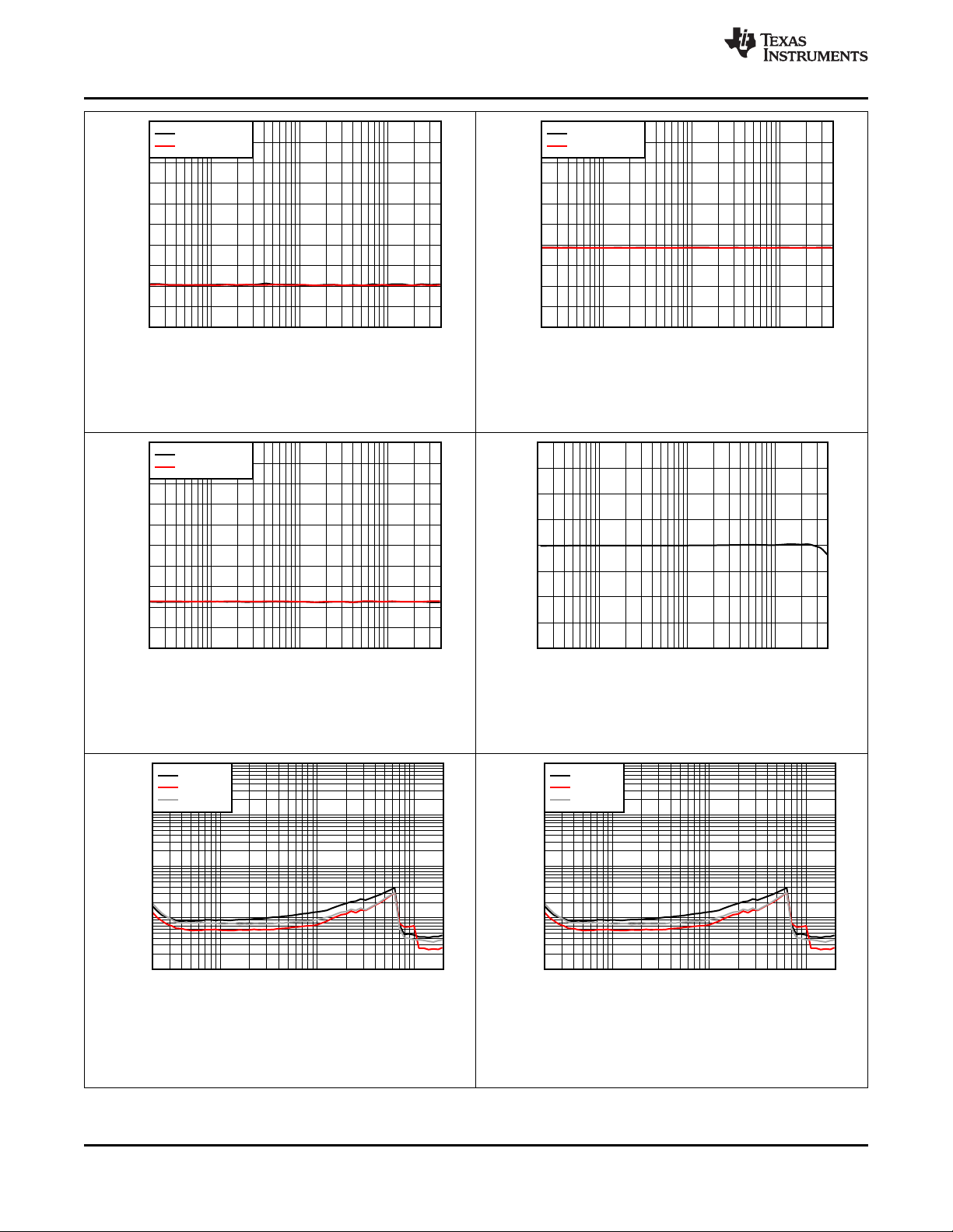
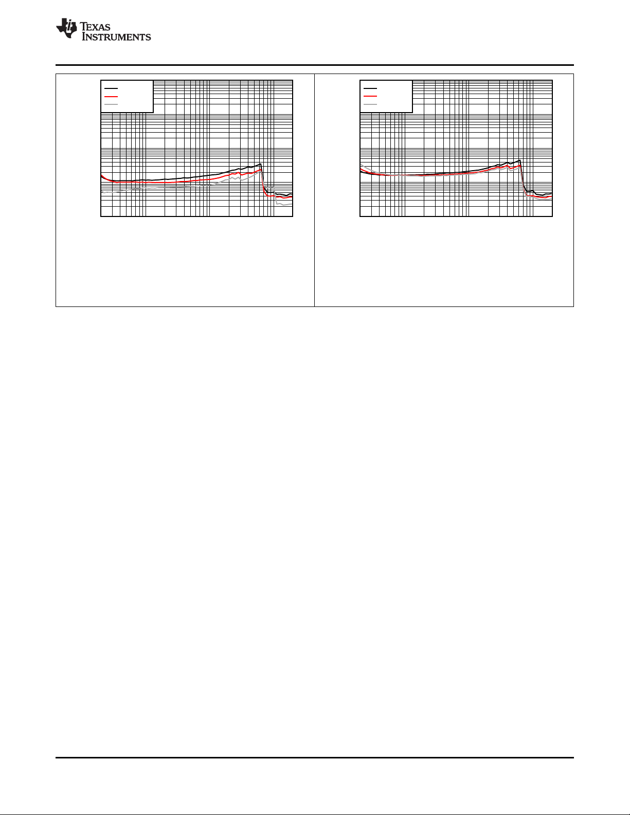
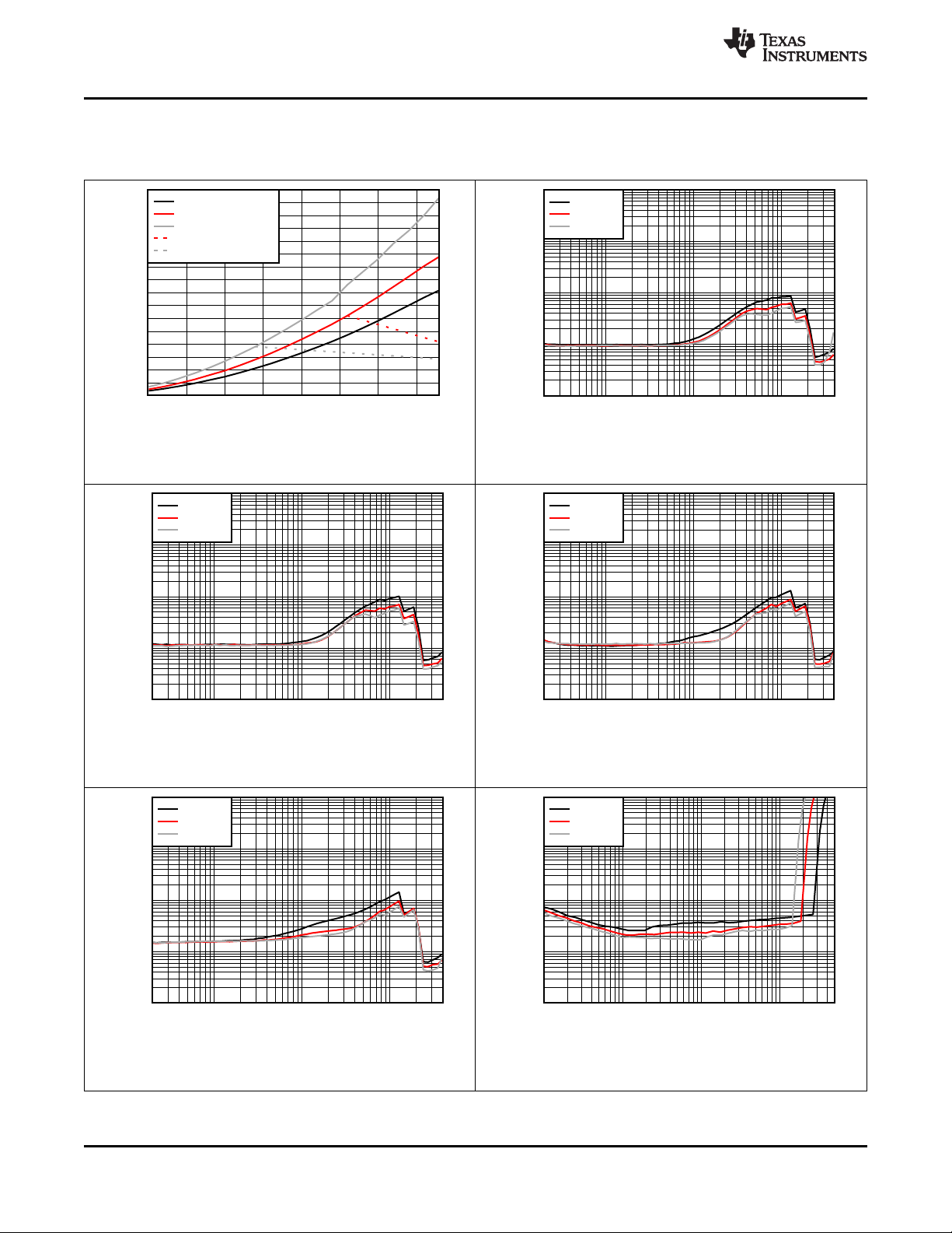
All performance plots were taken using the TAS5782MEVM Board at room temperature, unless otherwise noted.
The term "traditional LC filter" refers to the output filter that is present by default on the TAS5782MEVM Board.
Table 1. Quick Reference Table
OUTPUT
CONFIGURATIONS
Bridge Tied Load (BTL)
Configuration Curves
Parallel Bridge Tied Load
(PBTL) Configuration
Frequency Response Figure 42
Output Power vs PVDD Figure 23
THD+N vs Frequency, V
THD+N vs Frequency, V
THD+N vs Frequency, V
THD+N vs Frequency, V
THD+N vs Power, V
THD+N vs Power, V
THD+N vs Power, V
THD+N vs Power, V
Idle Channel Noise vs PVDD Figure 32
Efficiency vs Output Power Figure 33
Efficiency vs Output Power Figure 34
Efficiency vs Output Power Figure 35
Idle Current Draw (Filterless) vs PVDD Figure 36
Crosstalk vs. Frequency Figure 37
PVDD PSRR vs Frequency Figure 38
DVDD PSRR vs Frequency Figure 39
AVDD PSRR vs Frequency Figure 40
CPVDD PSRR vs Frequency Figure 41
THD+N vs Frequency, V
THD+N vs Frequency, V
THD+N vs Frequency, V
THD+N vs Frequency, V
Output Power vs PVDD Figure 47
THD+N vs Frequency, V
THD+N vs Frequency, V
THD+N vs Frequency, V
THD+N vs Frequency, V
THD+N vs Power, V
THD+N vs Power, V
THD+N vs Power, V
THD+N vs Power, V
Idle Channel Noise vs PVDD Figure 56
Efficiency vs Output Power Figure 57
THD+N vs Frequency, V
THD+N vs Frequency, V
THD+N vs Frequency, V
THD+N vs Frequency, V
PLOT TITLE FIGURE NUMBER
= 12 V Figure 24
PVDD
= 15 V Figure 25
PVDD
= 18 V Figure 26
PVDD
= 24 V Figure 27
PVDD
= 12 V Figure 28
PVDD
= 15 V Figure 29
PVDD
= 18 V Figure 30
PVDD
= 24 V Figure 31
PVDD
= 12 V Figure 43
PVDD
= 15 V Figure 44
PVDD
= 18 V Figure 45
PVDD
= 24 V Figure 46
PVDD
= 12 V Figure 48
PVDD
= 15 V Figure 49
PVDD
= 18 V Figure 50
PVDD
= 24 V Figure 51
PVDD
= 12 V Figure 52
PVDD
= 15 V Figure 53
PVDD
= 18 V Figure 54
PVDD
= 24 V Figure 55
PVDD
= 12 V Figure 60
PVDD
= 15 V Figure 61
PVDD
= 18 V Figure 62
PVDD
= 24 V Figure 63
PVDD
24
Submit Documentation Feedback Copyright © 2016–2017, Texas Instruments Incorporated
Product Folder Links: TAS5782M

Frequency (Hz)
THD+N (%)
0.001
0.01
0.1
1
10
100 1k 10k20 40k
D004
4 : Load
6 : Load
8 : Load
Frequency (Hz)
THD+N (%)
0.001
0.01
0.1
1
10
100 1k 10k20 40k
D005
4 : Load
6 : Load
8 : Load
Supply Voltage (V)
Output Power (W)
5 10 15 20 24
0
20
40
60
80
10 20
D002
8 : Load Peak
6 : Load Peak
4 : Load Peak
6 : Load Continous
4 : Load Continous
Frequency (Hz)
THD+N (%)
0.001
0.01
0.1
1
10
100 1k 10k20 40k
D003
4 : Load
6 : Load
8 : Load
TAS5782M
www.ti.com
SLASEG8A –MARCH 2016–REVISED JULY 2017
7.13.1 Bridge Tied Load (BTL) Configuration Curves
Free-air room temperature 25°C (unless otherwise noted) Measurements were made using TAS5782MEVM
board and Audio Precision System 2722 with Analog Analyzer filter set to 40-kHz brickwall filter. All
measurements taken with audio frequency set to 1 kHz and device PWM frequency set to 768 kHz, unless
otherwise noted. For both the BTL plots and the PBTL plots, the LC filter used was 4.7 µH / 0.68 µF. Return to
Quick Reference Table.
A
V(SPK_AMP)
A
V(SPK_AMP)
= 26 dBV
Figure 23. Output Power vs PVDD – BTL
= 20 dBV PO= 1 W V
Figure 25. THD+N vs Frequency – BTL
PVDD
= 15 V
A
V(SPK_AMP)
A
V(SPK_AMP)
= 20 dBV PO= 1 W V
Figure 24. THD+N vs Frequency – BTL
= 26 dBV PO= 1 W V
Figure 26. THD+N vs Frequency – BTL
PVDD
PVDD
= 12 V
= 18 V
Product Folder Links: TAS5782M
Submit Documentation FeedbackCopyright © 2016–2017, Texas Instruments Incorporated
25

Output Power (W)
Total Harmonic Distortion + Noise (%)
0.001
0.01
0.1
1
10
10m 100m 1 10 50
D010
4 : Load
6 : Load
8 : Load
Supply Voltage (V)
Idle Channel Noise (PVrms)
0
10
20
30
40
50
60
70
80
90
100
1510 20
D011
Gain = 20 dB, PWM Freq = 384 kHz
Gain = 26 dB, PWM Freq = 384 kHz
Gain = 20 dB, PWM Freq = 768 kHz
Gain = 26 dB, PWM Freq = 768 kHz
Output Power (W)
Total Harmonic Distortion + Noise (%)
0.001
0.01
0.1
1
10
10m 100m 1 10 40
D008
4 : Load
6 : Load
8 : Load
Output Power (W)
Total Harmonic Distortion + Noise (%)
0.001
0.01
0.1
1
10
10m 100m 1 10 50
D009
4 : Load
6 : Load
8 : Load
Frequency (Hz)
THD+N (%)
0.001
0.01
0.1
1
10
100 1k 10k20 40k
D006
4 : Load
6 : Load
8 : Load
Output Power (W)
Total Harmonic Distortion + Noise (%)
0.001
0.01
0.1
1
10
10m 100m 1 10 30
D007
4 : Load
6 : Load
8 : Load
TAS5782M
SLASEG8A –MARCH 2016–REVISED JULY 2017
www.ti.com
A
V(SPK_AMP)
A
V(SPK_AMP)
dBV
= 26 dBV PO= 1 W V
Figure 27. THD+N vs Frequency – BTL
= 20
Figure 29. THD+N vs Power – BTL
V
PVDD
PVDD
= 24 V
= 15 V
A
V(SPK_AMP)
A
V(SPK_AMP)
dBV
= 20 dBV V
Figure 28. THD+N vs Power – BTL
= 26
Figure 30. THD+N vs Power – BTL
PVDD
= 12 V
V
PVDD
=
18 V
A
V(SPK_AMP)
26
= 26 dBV V
Figure 31. THD+N vs Power – BTL
Submit Documentation Feedback Copyright © 2016–2017, Texas Instruments Incorporated
= 24 V
PVDD
Product Folder Links: TAS5782M
R
= 4 Ω
SPK
Figure 32. Idle Channel Noise vs PVDD – BTL

Frequency (Hz)
Crosstalk (dB)
-120
-100
-80
-60
-40
-20
0
100 1k 10k20 40k
D016
Ch 1 to Ch 2
Ch 2 to Ch 1
Frequency
PSRR (dB)
-100
-80
-60
-40
-20
0
100 1k 10k20 40k
D017
Left Channel
Right Channel
Output Power (W)
Efficiency (%)
0
10
20
30
40
50
60
70
80
90
100
0 20 40 60 80
D014
PVDD = 12 V
PVDD = 15 V
PVDD = 18 V
PVDD = 24 V
Supply Voltage (V)
PVDD Idle Current (mA)
0
10
20
30
40
50
60
205 15 2510 20
D015
Output Power (W)
Efficiency (%)
0
10
20
30
40
50
60
70
80
90
100
0 20 40 60 80
D012
PVDD = 12 V
PVDD = 15 V
PVDD = 18 V
PVDD = 24 V
Output Power (W)
Efficiency (%)
0
10
20
30
40
50
60
70
80
90
100
0 20 40 60 80
D013
PVDD = 12 V
PVDD = 15 V
PVDD = 18 V
PVDD = 24 V
www.ti.com
R
= 4 Ω
SPK
Figure 33. Efficiency vs Output Power – BTL
TAS5782M
SLASEG8A –MARCH 2016–REVISED JULY 2017
R
= 6 Ω
SPK
Figure 34. Efficiency vs Output Power – BTL
R
SPK
Figure 35. Efficiency vs Output Power – BTL
A
V(SPK_AMP)
= 26 dBV V
Figure 37. Crosstalk vs Frequency – BTL
= 8 Ω
f
SPK_AMP
= 768 kHz R
Figure 36. Idle Current Draw (Filterless) vs V
PVDD
= 24 V
A
V(SPK_AMP)
Product Folder Links: TAS5782M
SPK
PVDD
= 26 dBV V
= 24 V + 250 mVac
PVDD
Figure 38. PVDD PSRR vs Frequency – BTL
Submit Documentation FeedbackCopyright © 2016–2017, Texas Instruments Incorporated
= 8 Ω
– BTL
27
Frequency (Hz)
THD+N (%)
0.001
0.01
0.1
1
10
100 1k 10k20 20k
D035
4 : Load
6 : Load
8 : Load
Frequency (Hz)
THD+N (%)
0.001
0.01
0.1
1
10
100 1k 10k20 20k
D036
4 : Load
6 : Load
8 : Load
Frequency
PSRR (dB)
-100
-80
-60
-40
-20
0
100 1k 10k20 40k
D020
Left Channel
Right Channel
Frequency (Hz)
Gain (dB)
12
16
20
24
28
100 1k 10k20 40k
D001
Frequency
PSRR (dB)
-100
-80
-60
-40
-20
0
100 1k 10k20 40k
D018
Left Channel
Right Channel
Frequency
PSRR (dB)
-100
-80
-60
-40
-20
0
100 1k 10k20 40k
D019
Left Channel
Right Channel
TAS5782M
SLASEG8A –MARCH 2016–REVISED JULY 2017
www.ti.com
A
V(SPK_AMP)
V
= 3.3 V + 250 mVac
DVDD
A
V(SPK_AMP)
V
= 3.3 V + 250 mVac
CPVDD
= 26 dBV V
PVDD
Figure 39. DVDD PSRR vs Frequency – BTL
= 26 dBV V
PVDD
Figure 41. CPVDD PSRR vs Frequency – BTL
= 24 V
= 24 V
A
V(SPK_AMP)
V
= 3.3 V + 250 mVac
AVDD
A
V(SPK_AMP)
= 26 dBV V
PVDD
Figure 40. AVDD PSRR vs Frequency – BTL
= 20 dB P
= 1 W PVDD = 12 V
OUT
Figure 42. Gain vs Frequency – BTL
= 24 V
A
V(SPK_AMP)
dB
= 20
P
= 1 W PVDD = 12 V
OUT
Figure 43. THD vs Frequency – BTL
28
Submit Documentation Feedback Copyright © 2016–2017, Texas Instruments Incorporated
A
V(SPK_AMP)
dB
Product Folder Links: TAS5782M
= 20
P
= 1 W PVDD = 15 V
OUT
Figure 44. THD vs Frequency - BTL
Frequency (Hz)
THD+N (%)
0.001
0.01
0.1
1
10
100 1k 10k20 20k
D037
4 : Load
6 : Load
8 : Load
Frequency (Hz)
THD+N (%)
0.001
0.01
0.1
1
10
100 1k 10k20 20k
D038
4 : Load
6 : Load
8 : Load
www.ti.com
TAS5782M
SLASEG8A –MARCH 2016–REVISED JULY 2017
A
V(SPK_AMP)
dB
= 20
P
= 1 W PVDD = 18 V
OUT
Figure 45. THD vs Frequency – BTL
A
V(SPK_AMP)
dB
= 20
P
= 1 W PVDD = 24 V
OUT
Figure 46. THD vs Frequency – BTL
Submit Documentation FeedbackCopyright © 2016–2017, Texas Instruments Incorporated
29
Product Folder Links: TAS5782M
Frequency (Hz)
Total Harmonic Distortion + Noise (%)
0.001
0.01
0.1
1
10
100 1k 10k20 40k
D025
2 : Load
3 : Load
4 : Load
Output Power (W)
Total Harmonic Distortion + Noise (%)
0.001
0.01
0.1
1
10
10m 100m 1 10 50
D026
2 : Load
3 : Load
4 : Load
Frequency (Hz)
Total Harmonic Distortion + Noise (%)
0.001
0.01
0.1
1
10
100 1k 10k20 40k
D023
2 : Load
3 : Load
4 : Load
Frequency (Hz)
Total Harmonic Distortion + Noise (%)
0.001
0.01
0.1
1
10
100 1k 10k20 40k
D024
2 : Load
3 : Load
4 : Load
Supply Voltage (V)
Output Power (W)
5 10 15 20 24
0
20
40
60
80
100
120
140
160
10 20
D021
4 : Load Peak
3 : Load Peak
2 : Load Peak
3 : Load Continous
2 : Load Continous
Frequency (Hz)
Total Harmonic Distortion + Noise (%)
0.001
0.01
0.1
1
10
100 1k 10k20 40k
D022
2 : Load
3 : Load
4 : Load
TAS5782M
SLASEG8A –MARCH 2016–REVISED JULY 2017
7.13.2 Parallel Bridge Tied Load (PBTL) Configuration
Return to Quick Reference Table.
www.ti.com
A
V(SPK_AMP)
A
V(SPK_AMP)
= 26 dBV
Figure 47. Output Power vs PVDD – PBTL
= 20 dBV PO= 1 W V
PVDD
Figure 49. THD+N vs Frequency – PBTL
= 15 V
A
V(SPK_AMP)
A
V(SPK_AMP)
= 20 dBV PO= 1 W V
Figure 48. THD+N vs Frequency – PBTL
= 26 dBV PO= 1 W V
Figure 50. THD+N vs Frequency – PBTL
PVDD
PVDD
= 12 V
= 18 V
A
V(SPK_AMP)
= 26 dBV PO= 1 W V
Figure 51. THD+N vs Frequency – PBTL
30
Submit Documentation Feedback Copyright © 2016–2017, Texas Instruments Incorporated
= 24 V
PVDD
Product Folder Links: TAS5782M
A
V(SPK_AMP)
= 20 dBV V
Figure 52. THD+N vs Power – PBTL
PVDD
= 12 V

Output Power (W)
Efficiency (%)
0
10
20
30
40
50
60
70
80
90
0 20 40 60 80 100
D031
PVDD = 12 V
PVDD = 15 V
PVDD = 18 V
PVDD = 24 V
Output Power (W)
Efficiency (%)
0
10
20
30
40
50
60
70
80
90
100
0 20 40 60 80 100
D032
PVDD = 12 V
PVDD = 15 V
PVDD = 18 V
PVDD = 24 V
Output Power (W)
Total Harmonic Distortion + Noise (%)
0.001
0.01
0.1
1
10
10m 100m 1 10 150
D029
2 : Load
3 : Load
4 : Load
Supply Voltage (V)
Idle Channel Noise (PVrms)
0
10
20
30
40
50
60
70
80
90
100
205 15 2510 20
D030
Gain = 20 dB, PWM Freq = 384 kHz
Gain = 26 dB, PWM Freq = 384 kHz
Gain = 20 dB, PWM Freq = 768 kHz
Gain = 26 dB, PWM Freq = 768 kHz
Output Power (W)
Total Harmonic Distortion + Noise (%)
0.001
0.01
0.1
1
10
10m 100m 1 10 80
D027
2 : Load
3 : Load
4 : Load
Output Power (W)
Total Harmonic Distortion + Noise (%)
0.001
0.01
0.1
1
10
10m 100m 1 10 100
D028
2 : Load
3 : Load
4 : Load
www.ti.com
TAS5782M
SLASEG8A –MARCH 2016–REVISED JULY 2017
A
V(SPK_AMP)
A
V(SPK_AMP)
= 20 dBV V
Figure 53. THD+N vs Power – PBTL
= 20 dBV V
PVDD
= 24 V
Figure 55. THD+N vs Power – PBTL
PVDD
= 15 V
A
V(SPK_AMP)
R
= 4 Ω
SPK
= 26 dBV V
PVDD
= 18 V
Figure 54. THD+N vs Power – PBTL
Figure 56. Idle Channel Noise vs PVDD – PBTL
A
V(SPK_AMP)
dBV
= 26
Figure 57. Efficiency vs Output Power – PBTL
R
= 2 Ω
SPK
Product Folder Links: TAS5782M
A
V(SPK_AMP)
dBV
= 20
Figure 58. Efficiency vs Output Power
Submit Documentation FeedbackCopyright © 2016–2017, Texas Instruments Incorporated
R
= 3 Ω
SPK
31

Frequency (Hz)
THD+N (%)
0.001
0.01
0.1
1
10
100 1k 10k20 20k
D042
2 : Load
3 : Load
4 : Load
Frequency (Hz)
THD+N (%)
0.001
0.01
0.1
1
10
100 1k 10k20 20k
D040
2 : Load
3 : Load
4 : Load
Frequency (Hz)
THD+N (%)
0.001
0.01
0.1
1
10
100 1k 10k20 20k
D041
2 : Load
3 : Load
4 : Load
Output Power (W)
Efficiency (%)
0
10
20
30
40
50
60
70
80
90
100
0 20 40 60 80
D033
PVDD = 12 V
PVDD = 15 V
PVDD = 18 V
PVDD = 24 V
Frequency (Hz)
THD+N (%)
0.001
0.01
0.1
1
10
100 1k 10k20 20k
D039
2 : Load
3 : Load
4 : Load
TAS5782M
SLASEG8A –MARCH 2016–REVISED JULY 2017
www.ti.com
A
V(SPK_AMP)
dBV
A
V(SPK_AMP)
dB
= 20
Figure 59. Efficiency vs Output Power
= 20
P
= 1 W PVDD = 15 V
OUT
Figure 61. THD vs Frequency – PBTL
R
SPK
= 4 Ω
A
V(SPK_AMP)
dB
= 20
P
= 1 W PVDD = 12 V
OUT
Figure 60. THD vs Frequency – PBTL
A
V(SPK_AMP)
dB
= 20
P
= 1 W PVDD = 18 V
OUT
Figure 62. THD vs Frequency – PBTL
A
V(SPK_AMP)
32
= 20 dB P
Submit Documentation Feedback Copyright © 2016–2017, Texas Instruments Incorporated
= 1 W PVDD = 24 V
OUT
Figure 63. THD vs Frequency – PBTL
Product Folder Links: TAS5782M

www.ti.com
8 Parametric Measurement Information
PARAMETER FIGURE
Stereo BTL Figure 80
Mono PBTL Figure 81
TAS5782M
SLASEG8A –MARCH 2016–REVISED JULY 2017
Product Folder Links: TAS5782M
Submit Documentation FeedbackCopyright © 2016–2017, Texas Instruments Incorporated
33

SPK_OUTB+
SPK_OUTB-
SPK_OUTA+
SPK_OUTA-
SCLK
SDIN
MCLK
LRCK/FS
DVDD
CPVDD
GVDD_REG
PVDD
SPK_GAIN/FREQ
DAC_OUTA
DAC_OUTB
SPK_INB±
SPK_INA±
Internal Gate
Drive Regulator
RESETGPIO0 GPIO2 ADR1
CP
CN
DVDD_REG
CPVSS
Analog
to
PWM
Modulator
Gate
Drives
Full Bridge
Power
Stage A
Output
Current
Monitoring
and
Protection
Full Bridge
Power
Stage B
Gate
Drives
Closed Loop Class D Amplifier
1.8-V
Regulator
Internal Voltage
Supplies
Charge
Pump
Serial
Audio
Port
µCDSP
Selectable
Process
Flows
DAC
Internal Control Registers and State Machines
Clock Monitoring
and Error Protection
Die Temperature
Monitoring and Protection
ADR0SDASCL
SPK_FAULTSPK_SD
Error Reporting
SDOUT
AVDD
Internal
Voltage
Supplies
SPK_MUTE
Copyright © 2016, Texas Instruments Incorporated
TAS5782M
SLASEG8A –MARCH 2016–REVISED JULY 2017
www.ti.com
9 Detailed Description
9.1 Overview
The TAS5782M device integrates 4 main building blocks together into a single cohesive device that maximizes
sound quality, flexibility, and ease of use. The 4 main building blocks are listed below:
• A stereo audio DAC, boasting a strong Burr-Brown heritage with a highly flexible serial audio port.
• A µCDSP audio processing core, with different RAM and ROM options.
• A flexible closed-loop amplifier capable of operating in stereo or mono, at several different switching
frequencies, and with a variety of output voltages and loads.
• An I2C control port for communication with the device
The device requires only two power supplies for proper operation. A DVDD supply is required to power the lowvoltage digital and analog circuitry. Another supply, called PVDD, is required to provide power to the output stage
of the audio amplifier. The operating range for these supplies is shown in the Recommended Operating
Conditions table.
Communication with the device is accomplished through the I2C control port. A speaker amplifier fault line is also
provided to notify a system controller of the occurrence of an overtemperature , overcurrent, or DC error in the
speaker amplifier. Two digital GPIO pins are available for use. In the selectable process flows of the TAS5782M,
the GPIO2 pin is used as an SDOUT terminal. The other GPIO is unused.
The µCDSP audio processing core is pre-programmed with a configurable DSP program. The PPC3 provides a
means by which to manipulate the controls associated with that Process Flow.
9.2 Functional Block Diagram
34
Submit Documentation Feedback Copyright © 2016–2017, Texas Instruments Incorporated
Product Folder Links: TAS5782M

LRCK/FS
Serial Audio
Interface
(Input)
µCDSP
(including
interpolator)
Delta
Sigma
Modulator
Current
Segments
I to V
Line
Driver
fS 16 fS 128 fS
+
OSRCKDSPCK DACCK
Charge Pump
CPCK
Audio
Out
TAS5782M
www.ti.com
SLASEG8A –MARCH 2016–REVISED JULY 2017
9.3 Feature Description
9.3.1 Power-on-Reset (POR) Function
The TAS5782M device has a power-on reset function. The power-on reset feature resets all of the registers to
their default configuration as the device is powering up. When the low-voltage power supply used to power
DVDD, AVDD, and CPVDD exceeds the POR threshold, the device sets all of the internal registers to their
default values and holds them there until the device receives valid MCLK, SCLK, and LRCK/FS toggling for a
period of approximately 4 ms. After the toggling period has passed, the internal reset of the registers is removed
and the registers can be programmed via the I2C Control Port.
9.3.2 Device Clocking
The TAS5782M devices have flexible systems for clocking. Internally, the device requires a number of clocks,
mostly at related clock rates to function correctly. All of these clocks can be derived from the Serial Audio
Interface in one form or another.
Figure 64. Audio Flow with Respective Clocks
Figure 64 shows the basic data flow at basic sample rate (fS). When the data is brought into the serial audio
interface, the data is processed, interpolated and modulated to 128 × fSbefore arriving at the current segments
for the final digital to analog conversion.
Figure 65 shows the clock tree.
Product Folder Links: TAS5782M
Submit Documentation FeedbackCopyright © 2016–2017, Texas Instruments Incorporated
35

SCLK
PLL
K × R/P
K = J.D
J = 1,2,3,«..,62,63
D= 0000,0001,«.,9998,9999
R= 1,2,3,4,«.,15,16
P= 1,2,«.,14,15
SREF
(P0-R13)
MCLK/
PLL Mux
GPIO
MCLK
PLLCKIN PLLCK
MCLK
PLLEN
(P0-R4)
DAC CLK
Source Mux
DDAC
(P0-R28)
Divider
DDSP (P0-R27)
Divider
GPIO
MCLK
Divider
Divider
SDAC
(P0-R14)
DACCK (DAC Clock )
Divide
by 2
MUX
I16E (P0-R34)
OSRCK
(Oversampling
Ratio Clock )
DNCP (P0-R29)
CPCK (Charge Pump Clock )
DOSR
(P0-R30)
TAS5782M
SLASEG8A –MARCH 2016–REVISED JULY 2017
Feature Description (continued)
www.ti.com
Figure 65. TAS5782M Clock Distribution Tree
The Serial Audio Interface typically has 4 connection pins which are listed as follows:
• MCLK (System Master Clock)
• SCLK (Bit Clock)
• LRCK/FS (Left Right Word Clock and Frame Sync)
• SDIN (Input Data)
• The output data, SDOUT, is presented on one of the GPIO pins.
• See the GPIO Port and Hardware Control Pins section)
The device has an internal PLL that is used to take either MCLK or SCLK and create the higher rate clocks
required by the DSP and the DAC clock.
In situations where the highest audio performance is required, bringing MCLK to the device along with SCLK and
LRCK/FS is recommended. The device should be configured so that the PLL is only providing a clock source to
the DSP. All other clocks are then a division of the incoming MCLK. To enable the MCLK as the main source
clock, with all others being created as divisions of the incoming MCLK, set the DAC CLK source Mux (SDAC in
Figure 65) to use MCLK as a source, rather than the output of the MCLK/PLL Mux.
9.3.3 Serial Audio Port
9.3.3.1 Clock Master Mode from Audio Rate Master Clock
In Master Mode, the device generates bit clock and left-right and frame sync clock and outputs them on the
appropriate pins. To configure the device in master mode, first put the device into reset, then use registers
SCLKO and LRKO (P0-R9). Then reset the LRCK/FS and SCLK divider counters using bits RSCLK and RLRK
(P0-R12). Finally, exit reset.
Figure 66 shows a simplified serial port clock tree for the device in master mode.
36
Submit Documentation Feedback Copyright © 2016–2017, Texas Instruments Incorporated
Product Folder Links: TAS5782M

SCLK
LRCK/FS
MCLK
Divider
Q1 = 1...128
Audio Related System Clock (MCLK)
Divider
Q1 = 1...128
SCLKO (Bit Clock Output In Master Mode)
LRCK/FS (LR Clock or Frame Sync Output In
Master Mode
TAS5782M
www.ti.com
SLASEG8A –MARCH 2016–REVISED JULY 2017
Feature Description (continued)
Figure 66. Simplified Clock Tree for MCLK Sourced Master Mode
In master mode, MCLK is an input and SCLK and LRCK/FS are outputs. SCLK and LRCK/FS are integer
divisions of MCLK. Master mode with a non-audio rate master clock source requires external GPIO’s to use the
PLL in standalone mode. The PLL should be configured to ensure that the on-chip processor can be driven at
the maximum clock rate. The master mode of operation is described in the Clock Master from a Non-Audio Rate
Master Clock section.
When used with audio rate master clocks, the register changes that should be done include switching the device
into master mode, and setting the divider ratio. An example of the master mode of operations is using 24.576
MHz MCLK as a master clock source and driving the SCLK and LRCK/FS with integer dividers to create 48 kHz
sample rate clock output. In master mode, the DAC section of the device is also running from the PLL output.
The TAS5782M device is able to meet the specified audio performance while using the internal PLL. However,
using the MCLK CMOS oscillator source will have less jitter than the PLL.
To switch the DAC clocks (SDAC in the Figure 65) the following registers should be modified
• DAC and OSR Source Clock Register (P0-R14). Set to 0x30 (MCLK input, and OSR is set to whatever the
DAC source is)
• The DAC clock divider should be 16 fS.
– 16 × 48 kHz = 768 kHz
– 24.576 MHz (MCLK in) / 768 kHz = 32
– Therefore, the divide ratio for register DDAC (P0-R28) should be set to 32. The register mapping gives
0x00 = 1, therefore 32 must be converter to 0x1F (31dec).
9.3.3.2 Clock Master from a Non-Audio Rate Master Clock
The classic example here is running a 96-kHz sampling system. Given the clock tree for the device (shown in
Figure 65), a non-audio clock rate cannot be brought into the MCLK to the PLL in master mode. Therefore, the
PLL source must be configured to be a GPIO pin, and the output brought back into another GPIO pin.
Product Folder Links: TAS5782M
Submit Documentation FeedbackCopyright © 2016–2017, Texas Instruments Incorporated
37

SCLK
LRCK/FS
MCLK
Master Mode
SLCK Integer
Divider
Non-Audio MCLK
PLL
GPOIx
GPOIy
New
Audio
MCLK
Master Mode
LRCK/FS
Integer Divider
SCLK
Out
LRCK/FS
Out
TAS5782M
SLASEG8A –MARCH 2016–REVISED JULY 2017
Feature Description (continued)
www.ti.com
The clock flow through the system is shown in Figure 67. The newly generated MCLK must be brought out of the
device on a GPIO pin, then brought into the MCLK pin for integer division to create SCLK and LRCK/FS outputs.
9.3.3.3 Clock Slave Mode with 4-Wire Operation (SCLK, MCLK, LRCK/FS, SDIN)
The TAS5782M device requires a system clock to operate the digital interpolation filters and advanced segment
DAC modulators. The system clock is applied at the MCLK input and supports up to 50 MHz. The TAS5782M
device system-clock detection circuit automatically senses the system-clock frequency. Common audio sampling
frequencies in the bands of 32 kHz, (44.1 – 48 kHz), (88.2 – 96 kHz) are supported.
In the presence of a valid bit MCLK, SCLK and LRCK/FS, the device automatically configures the clock tree and
PLL to drive the µCDSP as required.
The sampling frequency detector sets the clock for the digital filter, Delta Sigma Modulator (DSM) and the
Negative Charge Pump (NCP) automatically. Table 2 shows examples of system clock frequencies for common
audio sampling rates.
Figure 67. Generating Audio Clocks Using Non-Audio Clock Sources
NOTE
Pull-up resistors should be used on SCLK and LRCK/FS in master mode to ensure the
device remains out of sleep mode.
NOTE
Values in the parentheses are grouped when detected, for example, 88.2 kHz and 96 kHz
are detected as double rate, 32 kHz, 44.1 kHz and 48 kHz are detected as single rate and
so on.
Also note, there is one process flow which has only a (1/2)X SRC.
38
Submit Documentation Feedback Copyright © 2016–2017, Texas Instruments Incorporated
Product Folder Links: TAS5782M

TAS5782M
www.ti.com
SLASEG8A –MARCH 2016–REVISED JULY 2017
Feature Description (continued)
MCLK rates that are not common to standard audio clocks, between 1 MHz and 50 MHz, are supported by
configuring various PLL and clock-divider registers directly. In slave mode, auto clock mode should be disabled
using P0-R37. Additionally, the user can be required to ignore clock error detection if external clocks are not
available for some time during configuration or if the clocks presented on the pins of the device are invalid. The
extended programmability allows the device to operate in an advanced mode in which the device becomes a
clock master and drive the host serial port with LRCK/FS and SCLK, from a non-audio related clock (for
example, using a setting of 12 MHz to generate 44.1 kHz [LRCK/FS] and 2.8224 MHz [SCLK]).
Table 2 shows the timing requirements for the system clock input. For optimal performance, use a clock source
with low phase jitter and noise. For MCLK timing requirements, refer to the Serial Audio Port Timing – Master
Mode section.
Table 2. System Master Clock Inputs for Audio Related Clocks
SAMPLING
FREQUENCY
8 kHz
16 kHz 2.048
32 kHz 4.096
44.1 kHz 5.6488
48 kHz 6.144
88.2 kHz 11.2896
96 kHz 12.288
(1) This system clock rate is not supported for the given sampling frequency.
(2) This system clock rate is supported by PLL mode.
64 f
See
S
(1)
SYSTEM CLOCK FREQUENCY (f
128 f
1.024
S
(2)
(2)
(2)
(2)
(2)
(2)
192 f
S
(2)
1.536
(2)
3.072
(2)
6.144
(2)
8.4672
(2)
9.216
(2)
16.9344 22.5792 33.8688 45.1584
18.432 24.576 36.864 49.152
256 f
2.048 3.072 4.096
4.096 6.144 8.192
8.192 12.288 16.384
11.2896 16.9344 22.5792
12.288 18.432 24.576
9.3.3.4 Clock Slave Mode with SCLK PLL to Generate Internal Clocks (3-Wire PCM)
S
MCLK
) (MHz)
384 f
S
512 f
S
9.3.3.4.1 Clock Generation using the PLL
The TAS5782M device supports a wide range of options to generate the required clocks as shown in Figure 65.
The clocks for the PLL require a source reference clock. This clock is sourced as the incoming SCLK or MCLK, a
GPIO can also be used.
The source reference clock for the PLL reference clock is selected by programming the SRCREF value on P0-
R13, D[6:4]. The TAS5782M device provides several programmable clock dividers to achieve a variety of
sampling rates. See Figure 65.
If PLL functionality is not required, set the PLLEN value on P0-R4, D[0] to 0. In this situation, an external master
clock is required.
Table 3. PLL Configuration Registers
CLOCK MULTIPLEXER
REGISTER FUNCTION BITS
SREF PLL Reference B0-P0-R13-D[6:4]
DDSP Clock divider B0-P0-R27-D[6:0]
DSCLK External SCLK Div B0-P0-R32-D[6:0]
DLRK External LRCK/FS Div B0-P0-R33-D[7:0]
Product Folder Links: TAS5782M
Submit Documentation FeedbackCopyright © 2016–2017, Texas Instruments Incorporated
39

PLLCKIN x R x J.D
PLLCK =
P
PLLCKIN x R x K
or PLLCK =
P
TAS5782M
SLASEG8A –MARCH 2016–REVISED JULY 2017
9.3.3.4.2 PLL Calculation
www.ti.com
The TAS5782M device has an on-chip PLL with fractional multiplication to generate the clock frequency required
by the Digital Signal Processing blocks. The programmability of the PLL allows operation from a wide variety of
clocks that may be available in the system. The PLL input (PLLCKIN) supports clock frequencies from 1 MHz to
50 MHz and is register programmable to enable generation of required sampling rates with fine precision.
The PLL is enabled by default. The PLL can be enabled by writing to P0-R4, D[0]. When the PLL is enabled, the
PLL output clock PLLCK is given by Equation 1:
where
• R = 1, 2, 3,4, ... , 15, 16
• J = 4,5,6, . . . 63, and D = 0000, 0001, 0002, . . . 9999
• K = [J value].[D value]
• P = 1, 2, 3, ... 15 (1)
R, J, D, and P are programmable. J is the integer portion of K (the numbers to the left of the decimal point), while
D is the fractional portion of K (the numbers to the right of the decimal point, assuming four digits of precision).
9.3.3.4.2.1 Examples:
• If K = 8.5, then J = 8, D = 5000
• If K = 7.12, then J = 7, D = 1200
• If K = 14.03, then J = 14, D = 0300
• If K = 6.0004, then J = 6, D = 0004
When the PLL is enabled and D = 0000, the following conditions must be satisfied:
• 1 MHz ≤ ( PLLCKIN / P ) ≤ 20 MHz
• 64 MHz ≤ (PLLCKIN x K x R / P ) ≤ 100 MHz
• 1 ≤ J ≤ 63
When the PLL is enabled and D ≠ 0000, the following conditions must be satisfied:
• 6.667 MHz ≤ PLLCLKIN / P ≤ 20 MHz
• 64 MHz ≤ (PLLCKIN x K x R / P ) ≤ 100 MHz
• 4 ≤ J ≤ 11
• R = 1
When the PLL is enabled,
• fS= (PLLCLKIN × K × R) / (2048 × P)
• The value of N is selected so that fS× N = PLLCLKIN x K x R / P is in the allowable range.
Example: MCLK = 12 MHz and fS= 44.1 kHz, (N=2048)
Select P = 1, R = 1, K = 7.5264, which results in J = 7, D = 5264
Example: MCLK = 12 MHz and fS= 48.0 kHz, (N=2048)
Select P = 1, R = 1, K = 8.192, which results in J = 8, D = 1920
Values are written to the registers in Table 4.
40
Submit Documentation Feedback Copyright © 2016–2017, Texas Instruments Incorporated
Table 4. PLL Registers
DIVIDER FUNCTION BITS
PLLE PLL enable P0-R4, D[0]
PPDV PLL P P0-R20, D[3:0]
PJDV PLL J P0-R21, D[5:0]
PDDV PLL D
PRDV PLL R P0-R24, D[3:0]
Product Folder Links: TAS5782M
P0-R22, D[5:0]
P0-R23, D[7:0]

www.ti.com
SLASEG8A –MARCH 2016–REVISED JULY 2017
Table 5. PLL Configuration Recommendations
EQUATIONS DESCRIPTION
fS(kHz) Sampling frequency
R
MCLK
MCLK (MHz) System master clock frequency at MCLK input (pin 20)
PLL VCO (MHz) PLL VCO frequency as PLLCK in Figure 65
P One of the PLL coefficients in Equation 1
PLL REF (MHz) Internal reference clock frequency which is produced by MCLK / P
M = K × R The final PLL multiplication factor computed from K and R as described in Equation 1
K = J.D One of the PLL coefficients in Equation 1
R One of the PLL coefficients in Equation 1
PLL f
S
DSP f
S
NMAC The clock divider value in Table 3
DSP CLK (MHz) The operating frequency as DSPCK in Figure 65
MOD f
S
MOD f (kHz) DAC operating frequency as DACCK in
NDAC DAC clock divider value in Table 3
DOSR
NCP NCP (negative charge pump) clock divider value in Table 3
CP f Negative charge pump clock frequency (fS× MOD fS/ NCP)
% Error
Ratio between sampling frequency and MCLK frequency (MCLK frequency = RMCLK x sampling frequency)
Ratio between fSand PLL VCO frequency (PLL VCO / fS)
Ratio between operating clock rate and fS(PLL fS/ NMAC)
Ratio between DAC operating clock frequency and fS(PLL fS/ NDAC)
OSR clock divider value in Table 3 for generating OSRCK in Figure 65. DOSR must be chosen so that MOD fS/ DOSR =
16 for correct operation.
Percentage of error between PLL VCO / PLL fSand fS(mismatch error).
• This value is typically zero but can be non-zero especially when K is not an integer (D is not zero).
• This value can be non-zero only when the TAS5782M device acts as a master.
TAS5782M
The previous equations explain how to calculate all necessary coefficients and controls to configure the PLL.
Table 6 provides for easy reference to the recommended clock divider settings for the PLL as a Master Clock.
Product Folder Links: TAS5782M
Submit Documentation FeedbackCopyright © 2016–2017, Texas Instruments Incorporated
41

TAS5782M
SLASEG8A –MARCH 2016–REVISED JULY 2017
f
S
(kHz)
8
11.025
16
R
MCLK
128 1.024 98.304 1 1.024 96 48 2 12288 1024 12 8.192 768 6144 16 48 0 4 1536
192 1.536 98.304 1 1.536 64 32 2 12288 1024 12 8.192 768 6144 16 48 0 4 1536
256 2.048 98.304 1 2.048 48 48 1 12288 1024 12 8.192 768 6144 16 48 0 4 1536
384 3.072 98.304 3 1.024 96 48 2 12288 1024 12 8.192 768 6144 16 48 0 4 1536
512 4.096 98.304 3 1.365 72 36 2 12288 1024 12 8.192 768 6144 16 48 0 4 1536
768 6.144 98.304 3 2.048 48 48 1 12288 1024 12 8.192 768 6144 16 48 0 4 1536
1024 8.192 98.304 3 2.731 36 36 1 12288 1024 12 8.192 768 6144 16 48 0 4 1536
1152 9.216 98.304 9 1.024 96 48 2 12288 1024 12 8.192 768 6144 16 48 0 4 1536
1536 12.288 98.304 9 1.365 72 36 2 12288 1024 12 8.192 768 6144 16 48 0 4 1536
2048 16.384 98.304 9 1.82 54 54 1 12288 1024 12 8.192 768 6144 16 48 0 4 1536
3072 24.576 98.304 9 2.731 36 36 1 12288 1024 12 8.192 768 6144 16 48 0 4 1536
128 1.4112 90.3168 1 1.411 64 32 2 8192 1024 8 11.2896 512 5644.8 16 32 0 4 1411.2
192 2.1168 90.3168 3 0.706 128 32 4 8192 1024 8 11.2896 512 5644.8 16 32 0 4 1411.2
256 2.8224 90.3168 1 2.822 32 32 1 8192 1024 8 11.2896 512 5644.8 16 32 0 4 1411.2
384 4.2336 90.3168 3 1.411 64 32 2 8192 1024 8 11.2896 512 5644.8 16 32 0 4 1411.2
512 5.6448 90.3168 3 1.882 48 48 1 8192 1024 8 11.2896 512 5644.8 16 32 0 4 1411.2
768 8.4672 90.3168 3 2.822 32 32 1 8192 1024 8 11.2896 512 5644.8 16 32 0 4 1411.2
1024 11.2896 90.3168 3 3.763 24 24 1 8192 1024 8 11.2896 512 5644.8 16 32 0 4 1411.2
1152 12.7008 90.3168 9 1.411 64 32 2 8192 1024 8 11.2896 512 5644.8 16 32 0 4 1411.2
1536 16.9344 90.3168 9 1.882 48 48 1 8192 1024 8 11.2896 512 5644.8 16 32 0 4 1411.2
2048 22.5792 90.3168 9 2.509 36 36 1 8192 1024 8 11.2896 512 5644.8 16 32 0 4 1411.2
3072 33.8688 90.3168 9 3.763 24 24 1 8192 1024 8 11.2896 512 5644.8 16 32 0 4 1411.2
128 2.048 98.304 1 2.048 48 48 1 6144 1024 6 16.384 384 6144 16 24 0 4 1536
192 3.072 98.304 1 3.072 32 32 1 6144 1024 6 16.384 384 6144 16 24 0 4 1536
256 4.096 98.304 1 4.096 24 24 1 6144 1024 6 16.384 384 6144 16 24 0 4 1536
384 6.144 98.304 3 2.048 48 48 1 6144 1024 6 16.384 384 6144 16 24 0 4 1536
512 8.192 98.304 3 2.731 36 36 1 6144 1024 6 16.384 384 6144 16 24 0 4 1536
768 12.288 98.304 3 4.096 24 24 1 6144 1024 6 16.384 384 6144 16 24 0 4 1536
1024 16.384 98.304 3 5.461 18 18 1 6144 1024 6 16.384 384 6144 16 24 0 4 1536
1152 18.432 98.304 3 6.144 16 16 1 6144 1024 6 16.384 384 6144 16 24 0 4 1536
1536 24.576 98.304 9 2.731 36 36 1 6144 1024 6 16.384 384 6144 16 24 0 4 1536
2048 32.768 98.304 9 3.641 27 27 1 6144 1024 6 16.384 384 6144 16 24 0 4 1536
3072 49.152 98.304 9 5.461 18 18 1 6144 1024 6 16.384 384 6144 16 24 0 4 1536
MCLK
(MHz)
64 1.024 98.304 1 1.024 96 48 2 6144 1024 6 16.384 384 6144 16 24 0 4 1536
PLL VCO
(MHz)
Table 6. Recommended Clock Divider Settings for PLL as Master Clock
P
PLL REF
(MHz)
M = K×R K = J×D R PLL fSDSP fSNMAC
DSP CLK
(MHz)
MOD f
S
MOD f
(kHz)
NDAC DOSR % ERROR NCP
www.ti.com
CP f
(kHz)
42
Submit Documentation Feedback Copyright © 2016–2017, Texas Instruments Incorporated
Product Folder Links: TAS5782M

www.ti.com
f
S
(kHz)
22.05
32
44.1
TAS5782M
SLASEG8A –MARCH 2016–REVISED JULY 2017
Table 6. Recommended Clock Divider Settings for PLL as Master Clock (continued)
R
MCLK
128 2.8224 90.3168 1 2.822 32 32 1 4096 1024 4 22.5792 256 5644.8 16 16 0 4 1411.2
192 4.2336 90.3168 3 1.411 64 32 2 4096 1024 4 22.5792 256 5644.8 16 16 0 4 1411.2
256 5.6448 90.3168 1 5.645 16 16 1 4096 1024 4 22.5792 256 5644.8 16 16 0 4 1411.2
384 8.4672 90.3168 3 2.822 32 32 1 4096 1024 4 22.5792 256 5644.8 16 16 0 4 1411.2
512 11.2896 90.3168 3 3.763 24 24 1 4096 1024 4 22.5792 256 5644.8 16 16 0 4 1411.2
768 16.9344 90.3168 3 5.645 16 16 1 4096 1024 4 22.5792 256 5644.8 16 16 0 4 1411.2
1024 22.5792 90.3168 3 7.526 12 12 1 4096 1024 4 22.5792 256 5644.8 16 16 0 4 1411.2
1152 25.4016 90.3168 9 2.822 32 32 1 4096 1024 4 22.5792 256 5644.8 16 16 0 4 1411.2
1536 33.8688 90.3168 9 3.763 24 24 1 4096 1024 4 22.5792 256 5644.8 16 16 0 4 1411.2
2048 45.1584 90.3168 9 5.018 18 18 1 4096 1024 4 22.5792 256 5644.8 16 16 0 4 1411.2
128 4.096 98.304 1 4.096 24 24 1 3072 1024 3 32.768 192 6144 16 12 0 4 1536
192 6.144 98.304 3 2.048 48 48 1 3072 1024 3 32.768 192 6144 16 12 0 4 1536
256 8.192 98.304 2 4.096 24 24 1 3072 1024 3 32.768 192 6144 16 12 0 4 1536
384 12.288 98.304 3 4.096 24 24 1 3072 1024 3 32.768 192 6144 16 12 0 4 1536
512 16.384 98.304 3 5.461 18 18 1 3072 1024 3 32.768 192 6144 16 12 0 4 1536
768 24.576 98.304 3 8.192 12 12 1 3072 1024 3 32.768 192 6144 16 12 0 4 1536
1024 32.768 98.304 3 10.923 9 9 1 3072 1024 3 32.768 192 6144 16 12 0 4 1536
1152 36.864 98.304 9 4.096 24 24 1 3072 1024 3 32.768 192 6144 16 12 0 4 1536
1536 49.152 98.304 6 8.192 12 12 1 3072 1024 3 32.768 192 6144 16 12 0 4 1536
128 5.6448 90.3168 1 5.645 16 16 1 2048 1024 2 45.1584 128 5644.8 16 8 0 4 1411.2
192 8.4672 90.3168 3 2.822 32 32 1 2048 1024 2 45.1584 128 5644.8 16 8 0 4 1411.2
256 11.2896 90.3168 2 5.645 16 16 1 2048 1024 2 45.1584 128 5644.8 16 8 0 4 1411.2
384 16.9344 90.3168 3 5.645 16 16 1 2048 1024 2 45.1584 128 5644.8 16 8 0 4 1411.2
512 22.5792 90.3168 3 7.526 12 12 1 2048 1024 2 45.1584 128 5644.8 16 8 0 4 1411.2
768 33.8688 90.3168 3 11.29 8 8 1 2048 1024 2 45.1584 128 5644.8 16 8 0 4 1411.2
1024 45.1584 90.3168 3 15.053 6 6 1 2048 1024 2 45.1584 128 5644.8 16 8 0 4 1411.2
MCLK
(MHz)
64 1.4112 90.3168 1 1.411 64 32 2 4096 1024 4 22.5792 256 5644.8 16 16 0 4 1411.2
32 1.024 98.304 1 1.024 96 48 2 3072 1024 3 32.768 192 6144 16 12 0 4 1536
48 1.536 98.304 1 1.536 64 16 4 3072 1024 3 32.768 192 6144 16 12 0 4 1536
64 2.048 98.304 1 2.048 48 24 2 3072 1024 3 32.768 192 6144 16 12 0 4 1536
32 1.4112 90.3168 1 1.411 64 32 2 2048 1024 2 45.1584 128 5644.8 16 8 0 4 1411.2
64 2.8224 90.3168 1 2.822 32 16 2 2048 1024 2 45.1584 128 5644.8 16 8 0 4 1411.2
PLL VCO
(MHz)
P
PLL REF
(MHz)
M = K×R K = J×D R PLL fSDSP fSNMAC
DSP CLK
(MHz)
MOD f
MOD f
S
(kHz)
NDAC DOSR % ERROR NCP
CP f
(kHz)
Product Folder Links: TAS5782M
Submit Documentation FeedbackCopyright © 2016–2017, Texas Instruments Incorporated
43

TAS5782M
SLASEG8A –MARCH 2016–REVISED JULY 2017
Table 6. Recommended Clock Divider Settings for PLL as Master Clock (continued)
f
(kHz)
48
96
S
R
MCLK
128 6.144 98.304 1 6.144 16 16 1 2048 1024 2 49.152 128 6144 16 8 0 4 1536
192 9.216 98.304 3 3.072 32 32 1 2048 1024 2 49.152 128 6144 16 8 0 4 1536
256 12.288 98.304 2 6.144 16 16 1 2048 1024 2 49.152 128 6144 16 8 0 4 1536
384 18.432 98.304 3 6.144 16 16 1 2048 1024 2 49.152 128 6144 16 8 0 4 1536
512 24.576 98.304 3 8.192 12 12 1 2048 1024 2 49.152 128 6144 16 8 0 4 1536
768 36.864 98.304 3 12.288 8 8 1 2048 1024 2 49.152 128 6144 16 8 0 4 1536
1024 49.152 98.304 3 16.384 6 6 1 2048 1024 2 49.152 128 6144 16 8 0 4 1536
128 12.288 98.304 2 6.144 16 16 1 1024 512 2 49.152 64 6144 16 4 0 4 1536
192 18.432 98.304 3 6.144 16 16 1 1024 512 2 49.152 64 6144 16 4 0 4 1536
256 24.576 98.304 4 6.144 16 16 1 1024 512 2 49.152 64 6144 16 4 0 4 1536
384 36.864 98.304 6 6.144 16 16 1 1024 512 2 49.152 64 6144 16 4 0 4 1536
512 49.152 98.304 8 6.144 16 16 1 1024 512 2 49.152 64 6144 16 4 0 4 1536
MCLK
(MHz)
32 1.536 98.304 1 1.536 64 32 2 2048 1024 2 49.152 128 6144 16 8 0 4 1536
64 3.072 98.304 1 3.072 32 16 2 2048 1024 2 49.152 128 6144 16 8 0 4 1536
32 3.072 98.304 1 3.072 32 16 2 1024 512 2 49.152 64 6144 16 4 0 4 1536
48 4.608 98.304 3 1.536 64 32 2 1024 512 2 49.152 64 6144 16 4 0 4 1536
64 6.144 98.304 1 6.144 16 8 2 1024 512 2 49.152 64 6144 16 4 0 4 1536
PLL VCO
(MHz)
P
PLL REF
(MHz)
M = K×R K = J×D R PLL fSDSP fSNMAC
DSP CLK
(MHz)
MOD f
www.ti.com
MOD f
S
(kHz)
NDAC DOSR % ERROR NCP
CP f
(kHz)
44
Submit Documentation Feedback Copyright © 2016–2017, Texas Instruments Incorporated
Product Folder Links: TAS5782M

TAS5782M
www.ti.com
SLASEG8A –MARCH 2016–REVISED JULY 2017
9.3.3.5 Serial Audio Port – Data Formats and Bit Depths
The serial audio interface port is a 3-wire serial port with the signals LRCK/FS (pin 25), SCLK (pin 23), and SDIN
(pin 24). SCLK is the serial audio bit clock, used to clock the serial data present on SDIN into the serial shift
register of the audio interface. Serial data is clocked into the TAS5782M device on the rising edge of SCLK. The
LRCK/FS pin is the serial audio left/right word clock or frame sync when the device is operated in TDM Mode.
Table 7. TAS5782M Audio Data Formats, Bit Depths and Clock Rates
FORMAT DATA BITS
I2S/LJ/RJ 32, 24, 20, 16 Up to 96 128 to 3072 (≤ 50 MHz) 64, 48, 32
TDM 32, 24, 20, 16
MAXIMUM LRCK/FS
FREQUENCY (kHz)
Up to 48 128 to 3072 125, 256
96 128 to 512 125, 256
MCLK RATE (fS) SCLK RATE (fS)
The TAS5782M device requires the synchronization of LRCK/FS and system clock, but does not require a
specific phase relation between LRCK/FS and system clock.
If the relationship between LRCK/FS and system clock changes more than ±5 MCLK, internal operation is
initialized within one sample period and analog outputs are forced to the bipolar zero level until resynchronization between LRCK/FS and system clock is completed.
If the relationship between LRCK/FS and SCLK are invalid more than 4 LRCK/FS periods, internal operation is
initialized within one sample period and analog outputs are forced to the bipolar zero level until resynchronization between LRCK/FS and SCLK is completed.
9.3.3.5.1 Data Formats and Master/Slave Modes of Operation
The TAS5782M device supports industry-standard audio data formats, including standard I2S and left-justified.
Data formats are selected via Register (P0-R40). All formats require binary two's complement, MSB-first audio
data; up to 32-bit audio data is accepted. The data formats are detailed in Figure 68 through Figure 73.
The TAS5782M device also supports right-justified, and TDM data. I2S, LJ, RJ, and TDM are selected using
Register (P0-R40). All formats require binary 2s complement, MSB-first audio data. Up to 32 bits are accepted.
Default setting is I2S and 24 bit word length. The I2S slave timing is shown in Figure 20.
shows a detailed timing diagram for the serial audio interface.
In addition to acting as a I2S slave, the TAS5782M device can act as an I2S master, by generating SCLK and
LRCK/FS as outputs from the MCLK input. Table 8 lists the registers used to place the device into Master or
Slave mode. Please refer to the Serial Audio Port Timing – Master Mode section for serial audio Interface timing
requirements in Master Mode. For Slave Mode timing, please refer to the Serial Audio Port Timing – Slave Mode
section.
Table 8. I2S Master Mode Registers
REGISTER FUNCTION
P0-R9-B0, B4, and B5 I2S Master mode select
P0-R32-D[6:0]
P0-R33-D[7:0]
SCLK divider and LRCK/FS divider
Product Folder Links: TAS5782M
Submit Documentation FeedbackCopyright © 2016–2017, Texas Instruments Incorporated
45

DATA
LRCK/FS
DATA
DATA
SCLK
161521 161521
2423
2
242321
323121 323121
1
«
1 t
S .
«
« ««
Left-channel Right-channel
« « «
«
«
««
Audio data word = 16-bit, SCLK = 32, 48, 64f
S
Audio data word = 24-bit, SCLK = 48, 64f
S
Audio data word = 32-bit, SCLK = 64f
S
MSB
LSB
MSB
LSB
MSB
LSB
MSB
LSB
MSB MSBLSB LSB
LRCK/FS
DATA
161521 161521
DATA
21 24
2
21 2423
DATA
21 3231 21 3231
Audio data word = 16-bit, SCLK = 32, 48, 64f
S
Audio data word = 24-bit, SCLK = 48, 64f
S
Audio data word = 32-bit, SCLK = 64f
S
1 t
S .
« « « « « «
Left-channel
««
««
Right-channel
LSB
MSB
LSB
MSB
LSB
MSB
LSB
MSB
MSB MSB
««
LSB
LSB
SCLK
TAS5782M
SLASEG8A –MARCH 2016–REVISED JULY 2017
www.ti.com
I2S Data Format; L-channel = LOW, R-channel = HIGH
Figure 68. Left Justified Audio Data Format
Figure 69. I2S Audio Data Format
46
Submit Documentation Feedback Copyright © 2016–2017, Texas Instruments Incorporated
Product Folder Links: TAS5782M

LRCK/FS
- ,
21 3231 21 3231
1
1
1
«
1 /f
S .
161521 161521
« « « «
21 2423 21 2423
Audio data word = 16-bit, Offset = 0
SCLK
DATA
DATA
DATA
Audio data word = 24-bit, Offset = 0
Audio data word = 32-bit, Offset = 0
Data Slot 1
MSB
LSB
MSB
LSB
Data Slot 2
« «
« «
«
MSB
LSB
«
MSB
LSB
Data Slot 1
MSB
LSB
LSB
LRCK/FS
DATA
DATA
DATA
21 3231 21 3231
1 /f
S .
« « « « « «
Left-channel
Right-channel
MSB
MSB
««
LSB
LSB
SCLK
Audio data word = 24-bit, SCLK = 48, 64f
S
Audio data word = 32-bit, SCLK = 64f
S
Audio data word = 16-bit, SCLK = 32, 48, 64f
S
161521
«
161521
«
MSB
LSB
21 24
2
«
MSB
LSB
21 2423
«
MSB
LSB
MSB
LSB
www.ti.com
The following data formats are only available in software mode.
TAS5782M
SLASEG8A –MARCH 2016–REVISED JULY 2017
Right Justified Data Format; L-channel = HIGH, R-channel = LOW
Figure 70. Right Justified Audio Data Format
TDM Data Format with OFFSET = 0
In TDM Modes, Duty Cycle of LRCK/FS should be 1x SCLK at minimum. Rising edge is considered frame start.
Figure 71. TDM 1 Audio Data Format
Product Folder Links: TAS5782M
Submit Documentation FeedbackCopyright © 2016–2017, Texas Instruments Incorporated
47

LRCK/FS
21 3231 21 3231
«
1 /f
S
.
161521 161521
« « « «
21 2423 21 2423
Audio data word = 16-bit, Offset = n
SCLK
DATA
DATA
DATA
Audio data word = 24-bit, Offset = n
Audio data word = 32-bit, Offset = n
Data Slot 1
MSB
LSB
MSB
LSB
Data Slot 2
« «
« «
«
MSB
LSB
«
MSB
LSB
Data Slot 1
MSB
LSB
LSB
Data Slot 2
Data Slot 1 Data Slot 2
OFFSET = n
LRCK/FS
21 3231 21 3231
1
1
1
«
1 /f
S .
161521 161521
« « « «
21 2423 21 2423
Audio data word = 16-bit, Offset = 1
SCLK
DATA
DATA
DATA
Audio data word = 24-bit, Offset = 1
Audio data word = 32-bit, Offset = 1
Data Slot 1
MSB
LSB
MSB
LSB
Data Slot 2
« «
« «
«
MSB
LSB
«
MSB
LSB
Data Slot 1
MSB
LSB
LSB
Data Slot 2
Data Slot 1 Data Slot 2
OFFSET = 1
TAS5782M
SLASEG8A –MARCH 2016–REVISED JULY 2017
www.ti.com
TDM Data Format with OFFSET = 1
In TDM Modes, Duty Cycle of LRCK/FS should be 1x SCLK at minimum. Rising edge is considered frame start.
Figure 72. TDM 2 Audio Data Format
TDM Data Format with OFFSET = N
In TDM Modes, Duty Cycle of LRCK/FS should be 1x SCLK at minimum. Rising edge is considered frame start.
48
Submit Documentation Feedback Copyright © 2016–2017, Texas Instruments Incorporated
Figure 73. TDM 3 Audio Data Format
Product Folder Links: TAS5782M

TAS5782M
www.ti.com
SLASEG8A –MARCH 2016–REVISED JULY 2017
9.3.3.6 Input Signal Sensing (Power-Save Mode)
The TAS5782M device has a zero-detect function. The zero-detect function can be applied to both channels of
data as an AND function or an OR function, via controls provided in the control port in P0-R65-D[2:1].Continuous
Zero data cycles are counted by LRCK/FS, and the threshold of decision for analog mute can be set by P0-R59,
D[6:4] for the data which is clocked in on the left frame of an I2S signal or Slot 1 of a TDM signal and P0-R59,
D[2:0] for the data which is clocked in on the right frame of an I2S signal or Slot 2 of a TDM signal as shown in
Table 10. Default values are 0 for both channels.
Table 9. Zero Detection Mode
ATMUTECTL VALUE FUNCTION
0
Bit : 2
1 (Default)
0
Bit : 1
1 (Default)
0
Bit : 0
1 (Default)
Zero data triggers for the two channels for zero detection are
ORed together.
Zero data triggers for the two channels for zero detection are
ANDed together.
Zero detection and analog mute are disabled for the data
clocked in on the right frame of an I2S signal or Slot 2 of a
TDM signal.
Zero detection analog mute are enabled for the data clocked in
on the right frame of an I2S signal or Slot 2 of a TDM signal.
Zero detection analog mute are disabled for the data clocked
in on the left frame of an I2S signal or Slot 1 of a TDM signal.
Zero detection analog mute are enabled for the data clocked in
on the left frame of an I2S signal or Slot 1 of a TDM signal.
Table 10. Zero Data Detection Time
ATMUTETIML OR ATMA NUMBER OF LRCK/FS CYCLES TIME at 48 kHz
0 0 0 1024 21 ms
0 0 1 5120 106 ms
0 1 0 10240 213 ms
0 1 1 25600 533 ms
1 0 0 51200 1.066 secs
1 0 1 102400 2.133 secs
1 1 0 256000 5.333 secs
1 1 1 512000 10.66 secs
9.3.4 Enable Device
To play audio after the device is powered up or reset the device must be enabled by writing book 0x00, page
0x00, register 0x02 to 0x00.
9.3.4.1 Example
The following is a sample script for enabling the device:
#Enable DUT
w 90 00 00 #Go to page 0
w 90 7f 00 #Go to book 0
w 90 02 00 #Enable device
9.3.5 Volume Control
For more information regarding the TAS5782 flexible processing system, see the TAS5782M Process Flows
9.3.5.1 DAC Digital Gain Control
Ramp-up frequency and ramp-down frequency can be controlled by P0-R63, D[7:6] and D[3:2] as shown in
Table 11. Also ramp-up step and ramp-down step can be controlled by P0-R63, D[5:4] and D[1:0] as shown in
Table 12.
Submit Documentation FeedbackCopyright © 2016–2017, Texas Instruments Incorporated
Product Folder Links: TAS5782M
49

TAS5782M
SLASEG8A –MARCH 2016–REVISED JULY 2017
www.ti.com
Table 11. Ramp Up or Down Frequency
RAMP UP
SPEED
00 1 Default 00 1 Default
01 2 01 2
10 4 10 4
11 Direct change 11 Direct change
EVERY N f
S
COMMENTS
RAMP DOWN
FREQUENCY
EVERY N f
S
COMMENTS
Table 12. Ramp Up or Down Step
RAMP UP
STEP
00 4.0 00 –4.0
01 2.0 01 –2.0
10 1.0 10 –1.0
11 0.5 Default 11 –0.5 Default
STEP dB COMMENTS
9.3.5.1.1 Emergency Volume Ramp Down
RAMP DOWN
STEP
STEP dB COMMENTS
Emergency ramp down of the volume is provided for situations such as I2S clock error and power supply failure.
Ramp-down speed is controlled by P0-R64-D[7:6]. Ramp-down step can be controlled by P0-R64-D[5:4]. Default
is ramp-down by every fScycle with –4dB step.
9.3.6 Adjustable Amplifier Gain and Switching Frequency Selection
The voltage divider between the GVDD_REG pin and the SPK_GAIN/FREQ pin is used to set the gain and
switching frequency of the amplifier. Upon start-up of the device, the voltage presented on the SPK_GAIN/FREQ
pin is digitized and then decoded into a 3-bit word which is interpreted inside the TAS5782M device to
correspond to a given gain and switching frequency. In order to change the SPK_GAIN or switching frequency of
the amplifier, the PVDD must be cycled off and on while the new voltage level is present on the
SPK_GAIN/FREQ pin.
Because the amplifier adds gain to both the signal and the noise present in the audio signal, the lowest gain
setting that can meet voltage-limited output power targets should be used. Using the lowest gain setting ensures
that the power target can be reached while minimizing the idle channel noise of the system. The switching
frequency selection affects three important operating characteristics of the device. The three affected
characteristics are the power dissipation in the device, the power dissipation in the inductor, and the target output
filter for the application.
Higher switching frequencies typically result in slightly higher power dissipation in the TAS5782M device and
lower dissipation in the inductor in the system, due to decreased ripple current through the inductor and
increased charging and discharging current in device and parasitic capacitances. Switching at the higher of the
available switching frequencies will result in lower overall dissipation in the system and lower operating
temperature of the inductors. However, the thermally limited power output of the device can be decreased in this
situation, because some of the TAS5782M device thermal headroom will be absorbed by the higher switching
frequency. Conversely inductor heating can be reduced by using the higher switching frequency to reduce the
ripple current.
Another advantage of increasing the switching frequency is that the higher frequency carrier signal can be filtered
by an L-C filter with a higher corner frequency, leading to physically smaller components. Use the highest
switching frequency that continues to meet the thermally limited power targets for the application. If thermal
constraints require heat reduction in the TAS5782M device, use a lower switching rate.
The switching frequency of the speaker amplifier is dependent on an internal synchronizing signal, (f
SYNC
), which
is synchronous with the sample rate. The rate of the synchronizing signal is also dependent on the sample rate.
Refer to Table 13 below for details regarding how the sample rates correlate to the synchronizing signal.
50
Submit Documentation Feedback Copyright © 2016–2017, Texas Instruments Incorporated
Product Folder Links: TAS5782M

TAS5782M
www.ti.com
SLASEG8A –MARCH 2016–REVISED JULY 2017
Table 13. Sample Rates vs Synchronization Signal
SAMPLE RATE
[kHz]
8
16
32
48
96
192
11.025
22.05
44.1
88.2
f
SYNC
[kHz]
96
88.2
Table 14 summarizes the de-code of the voltage presented to the SPK_GAIN/FREQ pin. The voltage presented
to the SPK_GAIN/FREQ pin is latched in upon startup of the device. Subsequent changes require power cycling
the device. A gain setting of 20 dB is recommended for nominal supply voltages of 13 V and lower, while a gain
of 26 dB is recommended for supply voltages up to 26.4 V. Table 14 shows the voltage required at the
SPK_GAIN/FREQ pin for various gain and switching scenarios as well some example resistor values for meeting
the voltage range requirements.
Table 14. Amplifier Switching Mode vs. SPK_GAIN/FREQ Voltage
V
SPK_GAIN/FREQ
MIN MAX
6.61 7 Reserved Reserved Reserved
5.44 6.6
4.67 5.43
3.89 4.66
3.11 3.88
2.33 3.1
1.56 2.32
0.78 1.55
0 0.77
(V) RESISTOR EXAMPLES
R100 (kΩ): RESISTOR TO
GROUND
R101 (kΩ): RESISTOR TO
GVDD_REG
R100 = 750
R101 = 150
R100 = 390
R101 = 150
R100 = 220
R101 = 150
R100 = 150
R101 = 150
R100 = 100
R101 = 150
R100 = 56
R101 = 150
R100 = 33
R101 = 150
R100 = 8.2
R101 = 150
GAIN MODE
26 dBV
20 dBV
AMPLIFIER
SWITCHING
FREQUENCY MODE
8 × f
SYNC
6 × f
SYNC
5 × f
SYNC
4 × f
SYNC
8 × f
SYNC
6 × f
SYNC
5 × f
SYNC
4 × f
SYNC
9.3.7 Error Handling and Protection Suite
9.3.7.1 Device Overtemperature Protection
The TAS5782M device continuously monitors die temperature to ensure the temperature does not exceed the
OTE
THRES
level specified in the Recommended Operating Conditions table. If an OTE event occurs, the
SPK_FAULT line is pulled low and the SPK_OUTxx outputs transition to high impedance, signifying a fault. This
is a non-latched error and the device will attempt to self clear after OTE
Product Folder Links: TAS5782M
CLRTIME
has passed.
Submit Documentation FeedbackCopyright © 2016–2017, Texas Instruments Incorporated
51

TAS5782M
SLASEG8A –MARCH 2016–REVISED JULY 2017
www.ti.com
9.3.7.2 SPK_OUTxx Overcurrent Protection
The TAS5782M device continuously monitors the output current of each amplifier output to ensure the output
current does not exceed the OCE
level specified in the Recommended Operating Conditions table. If an
THRES
OCE event occurs, the SPK_FAULT line is pulled low and the SPK_OUTxx outputs transition to high impedance,
signifying a fault. This is a non-latched error and the device will attempt to self clear after OCE
CLRTIME
has
passed.
9.3.7.3 DC Offset Protection
If the TAS5782M device measures a DC offset in the output voltage, the SPK_FAULT line is pulled low and the
SPK_OUTxx outputs transition to high impedance, signifying a fault. This latched error requires the SPK_MUTE
line to toggle to reset the error. Alternatively, pulling the MCLK, SCLK, or LRCK low causes a clock error, which
also resets the device. Normal operation resumes by re-starting the stopped lock.
9.3.7.4 Internal V
Undervoltage-Error Protection
AVDD
The TAS5782M device internally monitors the AVDD net to protect against the AVDD supply dropping
unexpectedly. To enable this feature, P1-R5-B0 is used.
9.3.7.5 Internal V
If the voltage presented on the PVDD supply drops below the UVE
Undervoltage-Error Protection
PVDD
THRES(PVDD)
value listed in the Recommended
Operating Conditions table, the SPK_OUTxx outputs transition to high impedance. This is a self-clearing error,
which means that once the PVDD level drops below the level listed in the Recommended Operating Conditions
table, the device resumes normal operation.
9.3.7.6 Internal V
If the voltage presented on the PVDD supply exceeds the OVE
Overvoltage-Error Protection
PVDD
THRES(PVDD)
value listed in the Recommended
Operating Conditions table, the SPK_OUTxx outputs will transition to high impedance. This is a self-clearing
error, which means that once the PVDD level drops below the level listed in the Recommended Operating
Conditions table, the device will resume normal operation.
NOTE
The voltage presented on the PVDD supply only protects up to the level described in the
Recommended Operating Conditions table for the PVDD voltage. Exceeding the absolute
maximum rating may cause damage and possible device failure, because the levels
exceed that which can be protected by the OVE protection circuit.
9.3.7.7 External Undervoltage-Error Protection
The SPK_MUTE pin can also be used to monitor a system voltage, such as a LCD TV backlight, a battery pack
in portable device, by using a voltage divider created with two resistors (see Figure 74).
• If the SPK_MUTE pin makes a transition from 1 to 0 over 6 ms or more, the device switches into external
undervoltage protection mode, which uses two trigger levels.
• When the SPK_MUTE pin level reaches 2 V, soft mute process begins.
• When the SPK_MUTE pin level reaches 1.2 V, analog output mute engages, regardless of digital audio level,
and analog output shutdown begins.
Figure 75 shows a timing diagram for external undervoltage error protection.
52
Submit Documentation Feedback Copyright © 2016–2017, Texas Instruments Incorporated
Product Folder Links: TAS5782M

t
f
0.9 × DV
DD
0.1 × DV
DD
2.0 V
1.2 V
Digital attenuation followed by analog mute
Analog mute
SPK_MUTE
V
DD
12 V
SPK_MUTE
7.25 NŸ
2.75 NŸ
TAS5782M
www.ti.com
SLASEG8A –MARCH 2016–REVISED JULY 2017
NOTE
The SPK_MUTE input pin voltage range is provided in the Recommended Operating
Conditions table. The ratio of external resistors must produce a voltage within the provided
input range. Any increase in power supply (such as power supply positive noise or ripple)
can pull the SPK_MUTE pin higher than the level specified in the Recommended
Operating Conditions table, potentially causing damage to or failure of the device.
Therefore, any monitored voltage (including all ripple, power supply variation, resistor
divider variation, transient spikes, and others) must be scaled by the resistor divider
network to never drive the voltage on the SPK_MUTE pin higher than the maximum level
specified in the Recommended Operating Conditions table.
When the divider is set correctly, any DC voltage can be monitored. Figure 74 shows a 12-V example of how the
SPK_MUTE is used for external undervoltage error protection.
Figure 74. SPK_MUTE Used in External Undervoltage Error Protection
Figure 75. SPK_MUTE Timing for External Undervoltage Error Protection
9.3.7.8 Internal Clock Error Notification (CLKE)
When a clock error is detected on the incoming data clock, the TAS5782M device switches to an internal
oscillator and continues to the drive the DAC, while attenuating the data from the last known value. Once this
process is complete, the DAC outputs will be hard muted to the ground and the class D PWM output will stop
switching. The clock error can be monitored at B0-P0-R94 and R95. The clock error status bits are non-latching,
except for MCLK halted B0-P0-R95-D[4] and CERF B0-P0-R95-D[0] which are cleared when read.
Product Folder Links: TAS5782M
Submit Documentation FeedbackCopyright © 2016–2017, Texas Instruments Incorporated
53

GPIOx Mux
Mux
GPIOx Input State
Monitoring
(P0-R119)
To µCDSP
GPIOx Output Inversion
P0-R87
GPIOx Output Enable
P0-R8
Internal Data
(P0-R83)
Off (low)
DSP GPIOx output
Register GPIOx output (P0-R86)
Auto mute flag (Both A and B)
Auto mute flag (Channel B)
Auto mute flag (Channel A)
Clock invalid flag
Serial Audio Data Output
Analog mute flag for B
Analog mute flag for A
PLL lock flag
Charge Pump Clock
Under voltage flag 1
Under voltage flag 2
PLL output/4
GPIOx Output Selection
P0-R83
To Clock Tree
TAS5782M
SLASEG8A –MARCH 2016–REVISED JULY 2017
9.3.8 GPIO Port and Hardware Control Pins
www.ti.com
9.3.9 I2C Communication Port
The TAS5782M device supports the I2C serial bus and the data transmission protocol for standard and fast mode
as a slave device. Because the TAS5782M register map spans several books and pages, the user must select
the correct book and page before writing individual register bits or bytes. Changing from book to book is
accomplished by first changing to page 0x00 by writing 0x00 to register 0x00 and then writing the book number
to register 0x7f of page 0. Changing from page to page is accomplished via register 0x00 on each page. The
register value selects the register page, from 0 to 255.
9.3.9.1 Slave Address
MSB LSB
1 0 0 1 0 ADR2 ADR1 R/ W
The TAS5782M device has 7 bits for the slave address. The first five bits (MSBs) of the slave address are
factory preset to 10010 (0x9x). The next two bits of the address byte are the device select bits which can be
user-defined by the ADR1 and ADR0 terminals. A maximum of four devices can be connected on the same bus
at one time, which gives a range of 0x90, 0x92, 0x94 and 0x96, as detailed in Table 16. Each TAS5782M device
responds when it receives the slave address.
ADR1 ADR0 I2C SLAVE ADDRESS [R/W]
0 0 0x90
0 1 0x92
54
1 0 0x94
1 1 0x96
Submit Documentation Feedback Copyright © 2016–2017, Texas Instruments Incorporated
Table 16. I2C Address Configuration via ADR0 and ADR1 Pins
Figure 76. GPIO Port
Table 15. I2C Slave Address
Product Folder Links: TAS5782M

9
SDA
SCL
St
Start
condition
1–7 8 1–8 9 1–8 9
9
Sp
Stop
condition
Slave address R/W ACK DATA ACK DATA ACK ACK
R/W: Read operation if 1; otherwise, write operation
ACK: Acknowledgement of a byte if 0
DATA: 8 bits (byte)
TAS5782M
www.ti.com
SLASEG8A –MARCH 2016–REVISED JULY 2017
9.3.9.2 Register Address Auto-Increment Mode
Auto-increment mode allows multiple sequential register locations to be written to or read back in a single
operation, and is especially useful for block write and read operations. The TAS5782M device supports autoincrement mode automatically. Auto-increment stops at page boundaries.
9.3.9.3 Packet Protocol
A master device must control packet protocol, which consists of start condition, slave address, read/write bit,
data if write or acknowledge if read, and stop condition. The TAS5782M device supports only slave receivers and
slave transmitters.
Figure 77. Packet Protocol
Table 17. Write Operation - Basic I2C Framework
Transmitter M M M S M S M S S M
Data Type St slave address R/ ACK DATA ACK DATA ACK ACK Sp
Table 18. Read Operation - Basic I2C Framework
Transmitter M M M S S M S M M M
Data Type St slave address R/ ACK DATA ACK DATA ACK NACK Sp
M = Master Device; S = Slave Device; St = Start Condition Sp = Stop Condition
9.3.9.4 Write Register
A master can write to any TAS5782M device registers using single or multiple accesses. The master sends a
TAS5782M device slave address with a write bit, a register address, and the data. If auto-increment is enabled,
the address is that of the starting register, followed by the data to be transferred. When the data is received
properly, the index register is incremented by 1 automatically. When the index register reaches 0x7F, the next
value is 0x0. Table 19 shows the write operation.
Table 19. Write Operation
Transmitter M M M S M S M S M S S M
Data Type St slave addr W ACK inc
reg
addr
ACK
write
data 1
ACK
write
data 2
ACK ACK Sp
M = Master Device; S = Slave Device; St = Start Condition Sp = Stop Condition; W = Write; ACK = Acknowledge
9.3.9.5 Read Register
A master can read the TAS5782M device register. The value of the register address is stored in an indirect index
register in advance. The master sends a TAS5782M device slave address with a read bit after storing the
register address. Then the TAS5782M device transfers the data which the index register points to. When autoincrement is enabled, the index register is incremented by 1 automatically. When the index register reaches
0x7F, the next value is 0x0. Table 20 lists the read operation.
Table 20. Read Operation
Transmitter M M M S M S M M M S S M M M
Product Folder Links: TAS5782M
Submit Documentation FeedbackCopyright © 2016–2017, Texas Instruments Incorporated
55

TAS5782M
SLASEG8A –MARCH 2016–REVISED JULY 2017
www.ti.com
Table 20. Read Operation (continued)
Data Type St
slave
addr
W ACK inc
reg
addr
ACK Sr
slave
addr
R ACK data ACK NACK Sp
M = Master Device; S = Slave Device; St = Start Condition; Sr = Repeated start condition; Sp = Stop Condition;
W = Write; R = Read; NACK = Not acknowledge
9.3.9.6 DSP Book, Page, and Register Update
The DSP memory is arranged in books, pages, and registers. Each book has several pages and each page has
several registers.
9.3.9.6.1 Book and Page Change
To change the book, the user must be on page 0x00. In register 0x7f on page 0x00 you can change the book.
On page 0x00 of each book, register 0x7f is used to change the book. Register 0x00 of each page is used to
change the page. To change a book first write 0x00 to register 0x00 to switch to page 0 then write the book
number to register 0x7f on page 0. To change between pages in a book, simply write the page number to
register 0x00.
9.3.9.6.2 Swap Flag
The swap flag is used to copy the audio coefficient from the host memory to the DSP memory. The swap flag
feature is important to maintain the stability of the BQs. A BQ is a closed-loop system with 5 coefficients. To
avoid instability in the BQ in an update transition between two different filters, update all five parameters within
one audio sample. The internal swap flag insures all 5 coefficients for each filter are transferred from host
memory to DSP memory occurs within an audio sample. The swap flag stays high until the full host buffer is
transferred to DSP memory. Updates to the Host buffer should not be made while the swap flag is high.
All writes to book 0x8C from page 0x11 and register 0x58 through page 0x21 and register 0x78 require the swap
flag. The swap flag is located in book 0x8C, page 0x23, and register 0x14 and must be set to 0x00 00 00 01 for
a swap.
9.3.9.6.3 Example Use
The following is a sample script for configuring a device on I2C slave address 0x90 and using the DSP host
memory to change the fine volume to the default value of 0 dB:
w 90 00 00 #Go to page 0
w 90 7f 8c #Change the book to 0x8C
w 90 00 1e #Go to page 0x1E
w 90 44 00 80 00 00 #Fine volume Left
w 90 48 00 80 00 00 #Fine volume Right
#Run the swap flag for the DSP to work on the new coefficients
w 90 00 00 #Go to page 0
w 90 7f 8c #Change the book to 0x8C
w 90 00 23 #Go to page 0x23
w 90 14 00 00 00 01 #Swap flag
9.4 Device Functional Modes
Because the TAS5782M device is a highly configurable device, numerous modes of operation can exist for the
device. For the sake of succinct documentation, these modes are divided into two modes:
• Fundamental operating modes
• Secondary usage modes
Fundamental operating modes are the primary modes of operation that affect the major operational
characteristics of the device, which are the most basic configurations that are chosen to ensure compatibility with
the intended application or the other components that interact with the device in the final system. Some
examples of the operating modes are the communication protocol used by the control port, the output
configuration of the amplifier, or the Master/Slave clocking configuration.
The fundamental operating modes are described starting in the Serial Audio Port Operating Modes section.
56
Submit Documentation Feedback Copyright © 2016–2017, Texas Instruments Incorporated
Product Folder Links: TAS5782M

TAS5782M
www.ti.com
SLASEG8A –MARCH 2016–REVISED JULY 2017
Device Functional Modes (continued)
Secondary usage modes are best described as modes of operation that are used after the fundamental operating
modes are chosen to fine tune how the device operates within a given system. These secondary usage modes
can include selecting between left justified and right justified Serial Audio Port data formats, or enabling some
slight gain/attenuation within the DAC path. Secondary usage modes are accomplished through manipulation of
the registers and controls in the I2C control port. Those modes of operation are described in their respective
register/bit descriptions and, to avoid redundancy, are not included in this section.
9.4.1 Serial Audio Port Operating Modes
The serial audio port in the TAS5782M device supports industry-standard audio data formats, including I2S, Time
Division Multiplexing (TDM), Left-Justified (LJ), and Right-Justified (RJ) formats. To select the data format that
will be used with the device, controls are provided on P0-R40. The timing diagrams for the serial audio port are
shown in the Serial Audio Port Timing – Slave Mode section, and the data formats are shown in the Serial Audio
Port – Data Formats and Bit Depths section.
9.4.2 Communication Port Operating Modes
The TAS5782M device is configured via an I2C communication port. The device does not support a hardware
only mode of operation, nor Serial Peripheral Interface (SPI) communication. The I2C Communication Protocol is
detailed in the I2C Communication Port section. The I2C timing requirements are described in the I2C Bus
Timing – Standard and I2C Bus Timing – Fast sections.
9.4.3 Speaker Amplifier Operating Modes
The TAS5782M device can be used in two different amplifier configurations:
• Stereo Mode
• Mono Mode
9.4.3.1 Stereo Mode
The familiar stereo mode of operation uses the TAS5782M device to amplify two independent signals, which
represent the left and right portions of a stereo signal. These amplified left and right audio signals are presented
on differential output pairs shown as SPK_OUTA± and SPK_OUTB±. The routing of the audio data which is
presented on the SPK_OUTxx outputs can be changed according to the Audio Process Flow which is used and
the configuration of registers P0-R42-D[5:4] and P0-R42-D[1:0]. The familiar stereo mode of operation is shown
in .
By default, the TAS5782M device is configured to output the Right frame of a I2S input on the Channel A output
and the left frame on the Channel B output.
9.4.3.2 Mono Mode
The mono mode of operation is used to describe operation in which the two outputs of the device are placed in
parallel with one another to increase the power sourcing capabilities of the audio output channel. This is also
known as Parallel Bridge Tied Load (PBTL).
On the output side of the TAS5782M device, the summation of the devices can be done before the filter in a
configuration called Pre-Filter PBTL. However, the two outputs may be required to merge together after the
inductor portion of the output filter. Doing so does require two additional inductors, but allows smaller, less
expensive inductors to be used because the current is divided between the two inductors. This process is called
Post-Filter PBTL. Both variants of mono operation are shown in Figure 78 and Figure 79.
Product Folder Links: TAS5782M
Submit Documentation FeedbackCopyright © 2016–2017, Texas Instruments Incorporated
57

L
FILT
C
FILT
L
FILT
C
FILT
SPK_OUTA+
SPK_OUTA-
SPK_OUTB+
L
FILT
C
FILT
SPK_OUTB-
L
FILT
C
FILT
Copyright © 2016, Texas Instruments Incorporated
L
FILT
C
FILT
L
FILT
C
FILT
SPK_OUTA+
SPK_OUTA-
SPK_OUTB+
SPK_OUTB-
Copyright © 2016, Texas Instruments Incorporated
TAS5782M
SLASEG8A –MARCH 2016–REVISED JULY 2017
www.ti.com
Device Functional Modes (continued)
Figure 78. Pre-Filter PBTL Figure 79. Post-Filter PBTL
On the input side of the TAS5782M device, the input signal to the mono amplifier can be selected from the any
slot in a TDM stream or the left or right frame from an I2S, LJ, or RJ signal. The TAS5782M device can also be
configured to amplify some mixture of two signals, as in the case of a subwoofer channel which mixes the left
and right channel together and sends the mixture through a low-pass filter to create a mono, low-frequency
signal.
The mono mode of operation is shown in the Mono (PBTL) Systems section.
9.4.3.3 Master and Slave Mode Clocking for Digital Serial Audio Port
The digital audio serial port in the TAS5782M device can be configured to receive clocks from another device as
a serial audio slave device. The slave mode of operation is described in the Clock Slave Mode with SCLK PLL to
Generate Internal Clocks (3-Wire PCM) section. If no system processor is available to provide the audio clocks,
the TAS5782M device can be placed into Master Mode. In master mode, the TAS5782M device provides the
clocks to the other audio devices in the system. For more details regarding the Master and Slave mode operation
within the TAS5782M device, see the Serial Audio Port Operating Modes section.
58
Submit Documentation Feedback Copyright © 2016–2017, Texas Instruments Incorporated
Product Folder Links: TAS5782M

TAS5782M
www.ti.com
SLASEG8A –MARCH 2016–REVISED JULY 2017
10 Application and Implementation
NOTE
Information in the following applications sections is not part of the TI component
specification, and TI does not warrant its accuracy or completeness. TI’s customers are
responsible for determining suitability of components for their purposes. Customers should
validate and test their design implementation to confirm system functionality.
10.1 Application Information
This section details the information required to configure the device for several popular configurations and
provides guidance on integrating the TAS5782M device into the larger system.
10.1.1 External Component Selection Criteria
The Supporting Component Requirements table in each application description section lists the details of the
supporting required components in each of the System Application Schematics.
Where possible, the supporting component requirements have been consolidated to minimize the number of
unique components which are used in the design. Component list consolidation is a method to reduce the
number of unique part numbers in a design, to ease inventory management, and to reduce the manufacturing
steps during board assembly. For this reason, some capacitors are specified at a higher voltage than what would
normally be required. An example of this is a 50-V capacitor may be used for decoupling of a 3.3-V power supply
net.
In this example, a higher voltage capacitor can be used even on the lower voltage net to consolidate all caps of
that value into a single component type. Similarly, several unique resistors that have all the same size and value
but different power ratings can be consolidated by using the highest rated power resistor for each instance of that
resistor value.
While this consolidation can seem excessive, the benefits of having fewer components in the design can far
outweigh the trivial cost of a higher voltage capacitor. If lower voltage capacitors are already available elsewhere
in the design, they can be used instead of the higher voltage capacitors. In all situations, the voltage rating of the
capacitors must be at least 1.45 times the voltage of the voltage which appears across them. The power rating of
the capacitors should be 1.5 times to 1.75 times the power dissipated in it during normal use case.
10.1.2 Component Selection Impact on Board Layout, Component Placement, and Trace Routing
Because the layout is important to the overall performance of the circuit, the package size of the components
shown in the component list was intentionally chosen to allow for proper board layout, component placement,
and trace routing. In some cases, traces are passed in between two surface mount pads or ground plane
extensions from the TAS5782M device and into to the surrounding copper for increased heat-sinking of the
device. While components may be offered in smaller or larger package sizes, it is highly recommended that the
package size remain identical to the size used in the application circuit as shown. This consistency ensures that
the layout and routing can be matched very closely, which optimizes thermal, electromagnetic, and audio
performance of the TAS5782M device in circuit in the final system.
10.1.3 Amplifier Output Filtering
The TAS5782M device is often used with a low-pass filter, which is used to filter out the carrier frequency of the
PWM modulated output. This filter is frequently referred to as the L-C Filter, due to the presence of an inductive
element L and a capacitive element C to make up the 2-pole filter.
The L-C filter removes the carrier frequency, reducing electromagnetic emissions and smoothing the current
waveform which is drawn from the power supply. The presence and size of the L-C filter is determined by several
system level constraints. In some low-power use cases that have no other circuits which are sensitive to EMI, a
simple ferrite bead or a ferrite bead plus a capacitor can replace the traditional large inductor and capacitor that
are commonly used. In other high-power applications, large toroid inductors are required for maximum power and
film capacitors can be used due to audio characteristics. Refer to the application report Class-D LC Filter Design
(SLOA119) for a detailed description on the proper component selection and design of an L-C filter based upon
the desired load and response.
Submit Documentation FeedbackCopyright © 2016–2017, Texas Instruments Incorporated
Product Folder Links: TAS5782M
59

TAS5782M
SLASEG8A –MARCH 2016–REVISED JULY 2017
www.ti.com
Application Information (continued)
10.1.4 Programming the TAS5782M
The TAS5782M device includes an I2C compatible control port to configure the internal registers of the
TAS5782M device. The control console software provided by TI is required to configure the device. More details
regarding programming steps, and a few important notes are available below and also in the design examples
that follow.
10.1.4.1 Resetting the TAS5782M Registers and Modules
The TAS5782M device has several methods by which the device can reset the register, interpolation filters, and
DAC modules. The registers offer the flexibility to do these in or out of shutdown as well as in or out of standby.
However, there can be issues if the reset bits are toggled in certain illegal operation modes.
Any of the following routines can be used with no issue:
• Reset Routine 1
– Place device in Standby
– Reset modules
• Reset Routine 2
– Place device in Standby + Power Down
– Reset registers
• Reset Routine 3
– Place device in Power Down
– Reset registers
• Reset Routine 4
– Place device in Standby
– Reset registers
• Reset Routine 5
– Place device in Standby + Power Down
– Reset modules + Reset registers
• Reset Routine 6
– Place device in Power Down
– Reset modules + Reset registers
• Reset Routine 7
– Place device in Standby
– Reset modules + Reset registers
Two reset routines are not supported and should be avoided. If used, they can cause the device to become
unresponsive. These unsupported routines are shown below.
• Unsupported Reset Routine 1 (do not use)
– Place device in Standby + Power Down
– Reset modules
• Unsupported Reset Routine 2 (do not use)
– Place device in Power Down
– Reset modules
60
Submit Documentation Feedback Copyright © 2016–2017, Texas Instruments Incorporated
Product Folder Links: TAS5782M

GND
GNDGNDGND
GND
GND GND
2.0-SDIN
2.0-SCLK
2.0-MCLK
2.0-SDOUT
2.0-GPIO1
2.0-GPIO0
2.0-SPK_FAULT
3.3V
GNDGND GND
1µF
C118
2.2µF
C113
GND
GND GND GND
PVDD
0.1µF
C121
2.0-SPK_OUTB-
2.0-SPK_OUTB+
L100
2.0-SPK_OUTA+
2.0-SPK_OUTA-
GND GND GND
PVDD
3.3V
GND
150k
R101
2.0-SCL
2.0-SDA
To System Processor
L101
L102
L103
22µF
C101
0.22µF
C104
GND
0.1µF
C109
GND
GND
GND
750k
R100
GND
BSTRPA-
1
SPK_OUTA-
2
PGND
3
SPK_OUTA+
4
BSTRAPA+
5
PVDD6PVDD
7
GVDO
8
SPK_GAIN/FREQ
9
AGND
10
SPK_INA-
11
SPK_INA+
12
DAC_OUTA
13
AVDD
14
AGND
15
SDA
16
SCL
17
GPIO018RESET
19
ADR1
20
GPIO2
21
MCLK
22
SCLK
23
SDIN
24
LRCK/FS25ADR026SPK_MUTE27DVDD_REG28DGND29DVDD30CPVDD31CP32GND33CN34CPVSS35DAC_OUTB36SPK_INB+37SPK_INB-38PGND39SPK_FAULT40PVDD41PVDD42PVDD43BSTRPB+44SPK_OUTB+45PGND46SPK_OUTB-47BSTRPB-
48
PAD
U100
TAS5782
2.0-OUTA+
2.0-OUTA-
2.0-OUTB-
2.0-OUTB+
2.0-SPK_MUTE
2.0-LRCK/FS
3.3V
1µF
C119
1µF
C120
1µF
C105
1µF
C103
22µF
C102
22µF
C122
22µF
C123
2.2µF
C114
0.22µF
C108
0.22µF
C111
0.22µF
C115
0.1µF
C110
0.1µF
C116
0.1µF
C117
2.2µF
C107
0.1µF
C100
1µF
C112
2.2µF
C106
Copyright © 2016, Texas Instruments Incorporated
TAS5782M
www.ti.com
SLASEG8A –MARCH 2016–REVISED JULY 2017
10.2 Typical Applications
10.2.1 2.0 (Stereo BTL) System
For the stereo (BTL) PCB layout, see Figure 85.
A 2.0 system refers to a system in which there are two full range speakers without a separate amplifier path for
the speakers which reproduce the low-frequency content. In this system, two channels are presented to the
amplifier via the digital input signal. These two channels are amplified and then sent to two separate speakers. In
some cases, the amplified signal is further separated based upon frequency by a passive crossover network after
the L-C filter. Even so, the application is considered 2.0.
Most commonly, the two channels are a pair of signals called a stereo pair, with one channel containing the
audio for the left channel and the other channel containing the audio for the right channel. While certainly the two
channels can contain any two audio channels, such as two surround channels of a multi-channel speaker
system, the most popular occurrence in two channels systems is a stereo pair.
Figure 80 shows the 2.0 (Stereo BTL) system application.
Submit Documentation FeedbackCopyright © 2016–2017, Texas Instruments Incorporated
10.2.1.1 Design Requirements
Figure 80. 2.0 (Stereo BTL) System Application Schematic
• Power supplies:
– 3.3-V supply
– 5-V to 24-V supply
• Communication: host processor serving as I2C compliant master
Product Folder Links: TAS5782M
• External memory (such as EEPROM and flash) used for coefficients
The requirements for the supporting components for the TAS5782M device in a Stereo 2.0 (BTL) system is
provided in Table 21.
61

TAS5782M
SLASEG8A –MARCH 2016–REVISED JULY 2017
Table 21. Supporting Component Requirements for Stereo 2.0 (BTL) Systems
REFERENCE
DESIGNATOR
U100 TAS5782M 48 Pin TSSOP Digital-input, closed-loop class-D amplifier
R100 See the Adjustable
R101 0402 1%, 0.063 W
L100, L101, L102,
L103
C100, C121 0.1 µF 0402
C104, C108, C111,
C115
C109, C110, C116,
C117
C103 1 µF
C105, C118, C119,
C120
C106, C107, C113,
C114
C101, C102, C122,
C123
VALUE SIZE DETAILED DESCRIPTION
Amplifier Gain and
Switching Frequency
Selection section
0.22 µF 0603
0.68 µF 0805
chosen to aid in trace
1 µF 0402 Ceramic, 1 µF, 6.3V, ±10%, X5R
2.2 µF 0402
22 µF 0805 Ceramic, 22 µF, ±20%, X5R
0402 1%, 0.063 W
See the Amplifier Output Filtering section
Ceramic, 0.1 µF, ±10%, X7R
Voltage rating must be > 1.45 × V
Ceramic, 0.22 µF, ±10%, X7R
Voltage rating must be > 1.45 × V
Ceramic, 0.68 µF, ±10%, X7R
Voltage rating must be > 1.8 × V
0603
(this body size
routing)
Ceramic, 1 µF, ±10%, X7R
Voltage rating must be > 16 V
Ceramic, 2.2 µF, ±10%, X5R
At a minimum, voltage rating must be > 10V, however higher
voltage caps have been shown to have better stability under DC
bias. Refer to the guidance provided in the TAS5782M for
suggested values.
Voltage rating must be > 1.45 × V
PVDD
PVDD
PVDD
PVDD
www.ti.com
10.2.1.2 Detailed Design Procedure
10.2.1.2.1 Step One: Hardware Integration
• Using the Typical Application Schematic as a guide, integrate the hardware into the system schematic.
• Following the recommended component placement, board layout, and routing given in the example layout
above, integrate the device and its supporting components into the system PCB file.
– The most critical sections of the circuit are the power supply inputs, the amplifier output signals, and the
high-frequency signals, all of which go to the serial audio port. Constructing these signals to ensure they
are given precedent as design trade-offs are made is recommended.
– For questions and support go to the E2E forums (e2e.ti.com). If deviating from the recommended layout is
necessary, go to the E2E forum to request a layout review.
10.2.1.2.2 Step Two: System Level Tuning
• Use the TAS5782MEVM evaluation module and the PPC3 app to configure the desired device settings.
10.2.1.2.3 Step Three: Software Integration
• Use the End System Integration feature of the PPC3 app to generate a baseline configuration file.
• Generate additional configuration files based upon operating modes of the end-equipment and integrate static
configuration information into initialization files.
• Integrate dynamic controls (such as volume controls, mute commands, and mode-based EQ curves) into the
main system program.
62
Submit Documentation Feedback Copyright © 2016–2017, Texas Instruments Incorporated
Product Folder Links: TAS5782M

www.ti.com
SLASEG8A –MARCH 2016–REVISED JULY 2017
10.2.1.3 Application Curves
Table 22 shows the application specific performance plots for Stereo 2.0 (BTL) systems.
Table 22. Relevant Performance Plots
PLOT TITLE FIGURE NUMBER
Output Power vs PVDD Figure 23
THD+N vs Frequency, V
THD+N vs Frequency, V
THD+N vs Frequency, V
THD+N vs Frequency, V
THD+N vs Power, V
THD+N vs Power, V
THD+N vs Power, V
THD+N vs Power, V
Idle Channel Noise vs PVDD Figure 32
Efficiency vs Output Power Figure 33
DVDD PSRR vs. Frequency Figure 39
AVDD PSRR vs. Frequency Figure 40
C
PSRR vs. Frequency Figure 41
PVDD
PVDD
PVDD
PVDD
PVDD
= 12 V Figure 24
PVDD
= 15 V Figure 25
PVDD
= 18 V Figure 26
PVDD
= 24 V Figure 27
PVDD
= 12 V Figure 28
= 15 V Figure 29
= 18 V Figure 30
= 24 V Figure 31
TAS5782M
10.2.2 Mono (PBTL) Systems
For the mono (PBTL) PCB layout, see Figure 87.
A mono system refers to a system in which the amplifier is used to drive a single loudspeaker. Parallel Bridge
Tied Load (PBTL) indicates that the two full-bridge channels of the device are placed in parallel and drive the
loudspeaker simultaneously using an identical audio signal. The primary benefit of operating the TAS5782M
device in PBTL operation is to reduce the power dissipation and increase the current sourcing capabilities of the
amplifier output. In this mode of operation, the current limit of the audio amplifier is approximately doubled while
the on-resistance is approximately halved.
The loudspeaker can be a full-range transducer or one that only reproduces the low-frequency content of an
audio signal, as in the case of a powered subwoofer. Often in this use case, two stereo signals are mixed
together and sent through a low-pass filter to create a single audio signal which contains the low frequency
information of the two channels. Conversely, advanced digital signal processing can create a low-frequency
signal for a multichannel system, with audio processing which is specifically targeted on low-frequency effects.
Because low-frequency signals are not perceived as having a direction (at least to the extent of high-frequency
signals) it is common to reproduce the low-frequency content of a stereo signal that is sent to two separate
channels. This configuration pairs one device in Mono PBTL configuration and another device in Stereo BTL
configuration in a single system called a 2.1 system. The Mono PBTL configuration is detailed in the 2.1 (Stereo
BTL + External Mono Amplifier) Systems section. shows the Mono (PBTL) system application
Product Folder Links: TAS5782M
Submit Documentation FeedbackCopyright © 2016–2017, Texas Instruments Incorporated
63

GND
GNDGNDGND
GND
GND
MONO-SDIN
MONO-SCLK
MONO-MCLK
MONO-SDOUT
MONO-GPIO1
MONO-GPIO0
MONO-SPK_FAULT
1µF
C212
3.3V
GNDGND GND
GND GND GND
0.1µF
C216
1µF
C210
MONO-SPK_OUTB
MONO-SPK_OUTA
GND GND
PVDD
0.1µF
C201
3.3V
2.2µF
C207
2.2µF
C206
MONO-SCL
MONO-SDA
22µF
C218
GND
0.1µF
C220
GND
0.1µF
C221
MONO_OUT+
1µF
C200
150k
R201
750k
R200
GND
GND
GND
MONO_OUT-
MONO-SPK_MUTE
MONO-LRCK/FS
0.22µF
C208
0.22µF
C209
0.22µF
C214
0.22µF
C215
To System Processor
49.9k
R202
BSTRPA-
1
SPK_OUTA-
2
PGND
3
SPK_OUTA+
4
BSTRAPA+
5
PVDD6PVDD
7
GVDO
8
SPK_GAIN/FREQ
9
AGND
10
SPK_INA-
11
SPK_INA+
12
DAC_OUTA
13
AVDD
14
AGND
15
SDA
16
SCL
17
GPIO018RESET
19
ADR1
20
GPIO2
21
MCLK
22
SCLK
23
SDIN
24
LRCK/FS25ADR026SPK_MUTE27DVDD_REG28DGND29DVDD30CPVDD31CP32GND33CN34CPVSS35DAC_OUTB36SPK_INB+37SPK_INB-38PGND39SPK_FAULT40PVDD41PVDD42PVDD43BSTRPB+44SPK_OUTB+45PGND46SPK_OUTB-47BSTRPB-
48
PAD
U200
TAS5782
L200
L201
1µF
C202
GND GND
GND
PVDD
390µF
C219
1µF
C217
1µF
C211
1µF
C213
1µF
C205
22µF
C203
390µF
C204
Copyright © 2016, Texas Instruments Incorporated
TAS5782M
SLASEG8A –MARCH 2016–REVISED JULY 2017
www.ti.com
Figure 81. Mono (PBTL) System Application Schematic
10.2.2.1 Design Requirements
• Power supplies:
– 3.3-V supply
– 5-V to 24-V supply
• Communication: Host processor serving as I2C compliant master
• External memory (EEPROM, flash, and others) used for coefficients.
The requirements for the supporting components for the TAS5782M device in a Mono (PBTL) system is provided
in Table 23.
REFERENCE
DESIGNATOR
U200 TAS5782M 48 Pin TSSOP Digital-input, closed-loop class-D amplifier with 96kHz processing
R200 See the Adjustable
R201 0402 1%, 0.063 W
R202 0402 1%, 0.063 W
L200, L201 See theAmplifier Output Filtering section
C216, C201 0.1 µF 0402
C208, C209, C214,
C215
C220, C221 0.68 µF 0805
64
Submit Documentation Feedback Copyright © 2016–2017, Texas Instruments Incorporated
Table 23. Supporting Component Requirements for Mono (PBTL) Systems
VALUE SIZE DETAILED DESCRIPTION
Amplifier Gain and
Switching Frequency
Selection section
0402 1%, 0.063 W
0.22 µF 0603
Product Folder Links: TAS5782M
Ceramic, 0.1 µF, ±10%, X7R
Voltage rating must be > 1.45 × V
Ceramic, 0.22 µF, ±10%, X7R
Voltage rating must be > 1.45 × V
Ceramic, 0.68 µF, ±10%, X7R
Voltage rating must be > 1.8 × V
PVDD
PVDD
PVDD

www.ti.com
Table 23. Supporting Component Requirements for Mono (PBTL) Systems (continued)
REFERENCE
DESIGNATOR
C200 1 µF
C205, C211, C213,
C212
C202, C217, C352,
C367
C206, C207 2.2 µF 0402
C203, C218
C204, C219
VALUE SIZE DETAILED DESCRIPTION
0603
(this body size
chosen to aid in trace
routing)
1 µF 0402 Ceramic, 1 µF, 6.3 V, ±10%, X5R
0805
1 µF
22 µF 0805 Ceramic, 22 µF, ±20%, X5R
390 µF 10 × 10 Aluminum, 390 µF, ±20%, 0.08-Ω
(this body size
chosen to aid in trace
routing)
TAS5782M
SLASEG8A –MARCH 2016–REVISED JULY 2017
Ceramic, 1 µF, ±10%, X7R
Voltage rating must be > 16 V
Ceramic, 1 µF, ±10%, X5R
Voltage rating must be > 1.45 × V
Ceramic, 2.2 µF, ±10%, X5R
At a minimum, voltage rating must be > 10V, however higher
voltage caps have been shown to have better stability under DC
bias please follow the guidance provided in the TAS5782M for
suggested values.
Voltage rating must be > 1.45 × V
Voltage rating must be > 1.45 × V
application circuit would be followed for higher power subwoofer
applications, these capacitors are added to provide local current
sources for low-frequency content. These capacitors can be
reduced or even removed based upon final system testing, including
critical listening tests when evaluating low-frequency designs.
PVDD
PVDD
Anticipating that this
PVDD
10.2.2.2 Detailed Design Procedure
10.2.2.2.1 Step One: Hardware Integration
• Using the Typical Application Schematic as a guide, integrate the hardware into the system schematic.
• Following the recommended component placement, board layout, and routing given in the example layout
above, integrate the device and its supporting components into the system PCB file.
– The most critical sections of the circuit are the power supply inputs, the amplifier output signals, and the
high-frequency signals, all of which go to the serial audio port. Constructing these signals to ensure they
are given precedent as design trade-offs are made is recommended.
– For questions and support go to the E2E forums (e2e.ti.com). If deviating from the recommended layout is
necessary, go to the E2E forum to request a layout review.
10.2.2.2.2 Step Two: System Level Tuning
• Use the TAS5782MEVM evaluation module and the PPC3 app to configure the desired device settings.
10.2.2.2.3 Step Three: Software Integration
• Use the End System Integration feature of the PPC3 app to generate a baseline configuration file.
• Generate additional configuration files based upon operating modes of the end-equipment and integrate static
configuration information into initialization files.
• Integrate dynamic controls (such as volume controls, mute commands, and mode-based EQ curves) into the
main system program.
Product Folder Links: TAS5782M
Submit Documentation FeedbackCopyright © 2016–2017, Texas Instruments Incorporated
65

TAS5782M
SLASEG8A –MARCH 2016–REVISED JULY 2017
www.ti.com
10.2.2.3 Application Specific Performance Plots for Mono (PBTL) Systems
Table 24 shows the application specific performance plots for Mono (PBTL) Systems
Table 24. Relevant Performance Plots
PLOT TITLE FIGURE NUMBER
Output Power vs PVDD Figure 47
THD+N vs Frequency, V
THD+N vs Frequency, V
THD+N vs Frequency, V
THD+N vs Frequency, V
THD+N vs Power, V
THD+N vs Power, V
THD+N vs Power, V
THD+N vs Power, V
Idle Channel Noise vs PVDD Figure 56
Efficiency vs Output Power Figure 57
PVDD
PVDD
PVDD
PVDD
= 12 V Figure 48
PVDD
= 15 V Figure 49
PVDD
= 18 V Figure 50
PVDD
= 24 V Figure 51
PVDD
= 12 V Figure 52
= 15 V Figure 53
= 18 V Figure 54
= 24 V Figure 55
10.2.3 2.1 (Stereo BTL + External Mono Amplifier) Systems
Figure 89 shows the PCB Layout for the 2.1 System.
To increase the low-frequency output capabilities of an audio system, a single subwoofer can be added to the
system. Because the spatial clues for audio are predominately higher frequency than that reproduced by the
subwoofer, often a single subwoofer can be used to reproduce the low frequency content of several other
channels in the system. This is frequently referred to as a dot one system. A stereo system with a subwoofer is
referred to as a 2.1 (two-dot-one), a 3 channel system with subwoofer is referred to as a 3.1 (three-dot-one), a
popular surround system with five speakers and one subwoofer is referred to as a 5.1, and so on.
10.2.3.1 Advanced 2.1 System (Two TAS5782M devices)
In higher performance systems, the subwoofer output can be enhanced using digital audio processing as was
done in the high-frequency channels. To accomplish this, two TAS5782M devices are used — one for the high
frequency left and right speakers and one for the mono subwoofer speaker. In this system, the audio signal can
be sent from the TAS5782M device through the SDOUT pin. Alternatively, the subwoofer amplifier can accept
the same digital input as the stereo, which might come from a central systems processor. Figure 82 shows the
2.1 (Stereo BTL + External Mono Amplifier) system application.
66
Submit Documentation Feedback Copyright © 2016–2017, Texas Instruments Incorporated
Product Folder Links: TAS5782M

2.1-SDOUT_LF
2.1-GPIO1
2.1-GPIO0_LF
2.1-SDIN
2.1-SCLK
2.1-MCLK
2.1-GPIO1_HF
2.1-GPIO0_HF
2.1-SPK_FAULT
2.1-SCL
2.1-SDA
ToSystem Processor
2.1-SPK_MUTE
2.1-LRCK/FS
GND
GNDGNDGND
GND
GND GND
3.3V
GNDGND GND
1µF
C318
2.2µF
C313
GND
GND GND GND
PVDD
0.1µF
C321
2.1-SPK_OUT1B-
2.1-SPK_OUT1B+
L300
2.1-SPK_OUT1A+
2.1-SPK_OUT1A-
GND GND GND
PVDD
3.3V
GND
150k
R301
L301
L302
L303
22µF
C301
0.22µF
C304
GND
0.1µF
C309
GND
GND
GND
750k
R300
GND
BSTRPA-
1
SPK_OUTA-
2
PGND
3
SPK_OUTA+
4
BSTRAPA+
5
PVDD6PVDD
7
GVDO
8
SPK_GAIN/FREQ
9
AGND
10
SPK_INA-
11
SPK_INA+
12
DAC_OUTA
13
AVDD
14
AGND
15
SDA
16
SCL
17
GPIO018RESET
19
ADR1
20
GPIO2
21
MCLK
22
SCLK
23
SDIN
24
LRCK/FS25ADR026SPK_MUTE27DVDD_REG28DGND29DVDD30CPVDD31CP32GND33CN34CPVSS35DAC_OUTB36SPK_INB+37SPK_INB-38PGND39SPK_FAULT40PVDD41PVDD42PVDD43BSTRPB+44SPK_OUTB+45PGND46SPK_OUTB-47BSTRPB-
48
PAD
U300
TAS5782
3.3V
1µF
C319
1µF
C320
1µF
C305
1µF
C303
22µF
C302
22µF
C322
22µF
C323
2.2µF
C314
0.22µF
C308
0.22µF
C311
0.22µF
C315
0.1µF
C310
0.1µF
C316
0.1µF
C317
2.2µF
C306
2.2µF
C307
0.1µF
C300
1µF
C312
2.1-HF_OUTA+
2.1-HF_OUTA-
2.1-HF_OUTB-
2.1-HF_OUTB+
GND
GNDGNDGND
GND
GND
1µF
C362
3.3V
GNDGND GND
GND GND GND
0.1µF
C366
1µF
C360
GND GND
PVDD
0.1µF
C351
3.3V
2.2µF
C357
2.2µF
C356
22µF
C353
22µF
C368
GND
0.1µF
C370
GND
0.1µF
C371
2.1_LF+
1µF
C350
150k
R351
750k
R350
GND
GND
GND
2.1_LF-
0.22µF
C358
0.22µF
C359
0.22µF
C364
0.22µF
C365
49.9k
R352
BSTRPA-
1
SPK_OUTA-
2
PGND
3
SPK_OUTA+
4
BSTRAPA+
5
PVDD6PVDD
7
GVDO
8
SPK_GAIN/FREQ
9
AGND
10
SPK_INA-
11
SPK_INA+
12
DAC_OUTA
13
AVDD
14
AGND
15
SDA
16
SCL
17
GPIO018RESET
19
ADR1
20
GPIO2
21
MCLK
22
SCLK
23
SDIN
24
LRCK/FS25ADR026SPK_MUTE27DVDD_REG28DGND29DVDD30CPVDD31CP32GND33CN34CPVSS35DAC_OUTB36SPK_INB+37SPK_INB-38PGND39SPK_FAULT40PVDD41PVDD42PVDD43BSTRPB+44SPK_OUTB+45PGND46SPK_OUTB-47BSTRPB-
48
PAD
U301
TAS5782
L350
L351
1µF
C352
GND GND
GND
PVDD
390µF
C354
390µF
C369
1µF
C367
1µF
C361
1µF
C363
2.1-SPK_OUT2A
2.1-SPK_OUT2B
1µF
C355
Copyright © 2016, Texas Instruments Incorporated
www.ti.com
TAS5782M
SLASEG8A –MARCH 2016–REVISED JULY 2017
Figure 82. 2.1 (Stereo BTL + External Mono Amplifier) Application Schematic
10.2.3.2 Design Requirements
• Power supplies:
– 3.3-V supply
– 5-V to 24-V supply
• Communication: Host processor serving as I2C compliant master
• External memory (EEPROM, flash, and others) used for coefficients.
The requirements for the supporting components for the TAS5782M device in a 2.1 (Stereo BTL + External Mono
Amplifier) system is provided in Table 25.
Product Folder Links: TAS5782M
Submit Documentation FeedbackCopyright © 2016–2017, Texas Instruments Incorporated
67

TAS5782M
SLASEG8A –MARCH 2016–REVISED JULY 2017
www.ti.com
Table 25. Supporting Component Requirements for 2.1 (Stereo BTL + External Mono Amplifier) Systems
REFERENCE
DESIGNATOR
U300 TAS5782M 48 Pin TSSOP Digital-input, closed-loop class-D amplifier 96kHz Processing
R300, R350 See the Adjustable
R301, R351 0402 1%, 0.063 W
R352 0402 1%, 0.063 W
L300, L301, L302,
L303
L350, L351
C394, C395, C396,
C397, C398, C399
C300, C321, C351,
C366
C304, C308, C311,
C315, C358, C359,
C364, C365
C309, C310, C316,
C317, C370, C371
C303, C350, C312,
C360
C305, C318, C319,
C320, C355, C361,
C363, C312, C362
C352, C367 1 µF 0805
C306, C307, C313,
C314, C356, C357,
C301, C302, C322,
C323, C353, C368
C354, C369 390 µF 10 × 10
VALUE SIZE DETAILED DESCRIPTION
0402 1%, 0.063 W
Amplifier Gain and
Switching Frequency
Selection section
See the Amplifier Output Filtering section
0.01 µF 0603 Ceramic, 0.01 µF, 50 V, +/-10%, X7R
0.1 µF 0402
0.22 µF 0603
0.68 µF 0805
1 µF 0603
Ceramic, 0.1 µF, ±10%, X7R
Voltage rating must be > 1.45 × V
Ceramic, 0.22 µF, ±10%, X7R
Voltage rating must be > 1.45 × V
Ceramic, 0.68 µF, ±10%, X7R
Voltage rating must be > 1.8 × V
Ceramic, 1 µF, ±10%, X7R
Voltage rating must be > 1.45 × V
1 µF 0402 Ceramic, 1 µF, 6.3V, ±10%, X5R
Ceramic, 1 µF, ±10%, X7R
Voltage rating must be > 1.45 × V
2.2 µF 0402
22 µF 0805
Ceramic, 2.2 µF, ±10%, X5R
Voltage rating must be > 1.45 × V
Ceramic, 22 µF, ±20%, X5R
Voltage rating must be > 1.45 × V
Aluminum, 390 µF, ±20%, 0.08 Ω
Voltage rating must be > 1.45 × V
PVDD
PVDD
PVDD
PVDD
PVDD
PVDD
PVDD
PVDD
68
Submit Documentation Feedback Copyright © 2016–2017, Texas Instruments Incorporated
Product Folder Links: TAS5782M

TAS5782M
www.ti.com
SLASEG8A –MARCH 2016–REVISED JULY 2017
10.2.3.3 Application Specific Performance Plots for 2.1 (Stereo BTL + External Mono Amplifier) Systems
Table 26 shows the application specific performance plots for 2.1 (Stereo BTL + External Mono Amplifier)
Systems
Table 26. Relevant Performance Plots
DEVICE PLOT TITLE FIGURE NUMBER
Output Power vs PVDD Figure 23
U300
U301
U300
and
U301
THD+N vs Frequency, V
THD+N vs Frequency, V
THD+N vs Frequency, V
THD+N vs Frequency, V
THD+N vs Power, V
THD+N vs Power, V
THD+N vs Power, V
THD+N vs Power, V
PVDD
PVDD
PVDD
PVDD
Idle Channel Noise vs PVDD Figure 32
Efficiency vs Output Power Figure 33
PVDD PSRR vs Frequency Figure 38
Output Power vs PVDD Figure 47
THD+N vs Frequency, V
THD+N vs Frequency, V
THD+N vs Frequency, V
THD+N vs Frequency, V
THD+N vs Power, V
THD+N vs Power, V
THD+N vs Power, V
THD+N vs Power, V
PVDD
PVDD
PVDD
PVDD
Idle Channel Noise vs PVDD Figure 56
Efficiency vs Output Power Figure 57
DVDD PSRR vs. Frequency Figure 39
AVDD PSRR vs. Frequency Figure 40
C
PSRR vs. Frequency Figure 41
PVDD
Powerdown Current Draw vs. PVDD Figure 47
= 12 V Figure 24
PVDD
= 15 V Figure 25
PVDD
= 18 V Figure 26
PVDD
= 24 V Figure 27
PVDD
= 12 V Figure 28
= 15 V Figure 29
= 18 V Figure 30
= 24 V Figure 31
= 12 V Figure 48
PVDD
= 15 V Figure 49
PVDD
= 18 V Figure 50
PVDD
= 24 V Figure 51
PVDD
= 12 V Figure 52
= 15 V Figure 53
= 18 V Figure 54
= 24 V Figure 55
Product Folder Links: TAS5782M
Submit Documentation FeedbackCopyright © 2016–2017, Texas Instruments Incorporated
69

Internal Analog Circuitry
Internal Digital
Circuitry
DAC Output Stage
(Negative)
DAC Output Stage
(Positive)
Internal Mixed
Signal Circuitry
Gate Drive
Voltage
Output Stage
Power Supply
External Filtering/Decoupling
External Filtering/Decoupling
External Filtering/Decoupling
+
±
AVDD
DVDD
CPVDD
LDO
Charge
Pump
PVDD
Linear
Regulator
+
±
PVDD
GVDD_REG
CPVSS
DVDD_REG
TAS5782M
SLASEG8A –MARCH 2016–REVISED JULY 2017
www.ti.com
11 Power Supply Recommendations
11.1 Power Supplies
The TAS5782M device requires two power supplies for proper operation. A high-voltage supply called PVDD is
required to power the output stage of the speaker amplifier and its associated circuitry. Additionally, one low-
voltage power supply which is called DVDD is required to power the various low-power portions of the device.
The allowable voltage range for both the PVDD and the DVDD supply are listed in the Recommended Operating
Conditions table. The two power supplies do not have a required powerup sequence. The power supplies can be
powered on in any order. TI recommends waiting 100 ms to 240 ms for the DVDD power supplies to stabilize
before starting I2C communication and providing stable I2S clock before enabling the device outputs.
Figure 83. Power Supply Functional Block Diagram
11.1.1 DVDD Supply
The DVDD supply that is required from the system is used to power several portions of the device. As shown in
Figure 83, it provides power to the DVDD pin, the CPVDD pin, and the AVDD pin. Proper connection, routing,
and decoupling techniques are highlighted in the Application and Implementation section and the Layout
Example section) and must be followed as closely as possible for proper operation and performance. Deviation
from the guidance offered in the TAS5782M device Application and Implementation section can result in reduced
performance, errant functionality, or even damage to the TAS5782M device.
Some portions of the device also require a separate power supply that is a lower voltage than the DVDD supply.
To simplify the power supply requirements for the system, the TAS5782M device includes an integrated lowdropout (LDO) linear regulator to create this supply. This linear regulator is internally connected to the DVDD
supply and its output is presented on the DVDD_REG pin, providing a connection point for an external bypass
capacitor. It is important to note that the linear regulator integrated in the device has only been designed to
support the current requirements of the internal circuitry, and should not be used to power any additional external
circuitry. Additional loading on this pin could cause the voltage to sag, negatively affecting the performance and
operation of the device.
70
Submit Documentation Feedback Copyright © 2016–2017, Texas Instruments Incorporated
Product Folder Links: TAS5782M

TAS5782M
www.ti.com
SLASEG8A –MARCH 2016–REVISED JULY 2017
Power Supplies (continued)
The outputs of the high-performance DACs used in the TAS5782M device are ground centered, requiring both a
positive low-voltage supply and a negative low-voltage supply. The positive power supply for the DAC output
stage is taken from the AVDD pin, which is connected to the DVDD supply provided by the system. A charge
pump is integrated in the TAS5782M device to generate the negative low-voltage supply. The power supply input
for the charge pump is the CPVDD pin. The CPVSS pin is provided to allow the connection of a filter capacitor
on the negative low-voltage supply. As is the case with the other supplies, the component selection, placement,
and routing of the external components for these low voltage supplies are shown in the TAS5782M and should
be followed as closely as possible to ensure proper operation of the device.
11.1.2 PVDD Supply
The output stage of the speaker amplifier drives the load using the PVDD supply. This is the power supply which
provides the drive current to the load during playback. Proper connection, routing, and decoupling techniques are
highlighted in the TAS5782MEVM and must be followed as closely as possible for proper operation and
performance. Due to the high-voltage switching of the output stage, it is particularly important to properly
decouple the output power stages in the manner described in the TAS5782M deviceApplication and
Implementation . Lack of proper decoupling, like that shown in the Application and Implementation , results in
voltage spikes which can damage the device.
A separate power supply is required to drive the gates of the MOSFETs used in the output stage of the speaker
amplifier. This power supply is derived from the PVDD supply via an integrated linear regulator. A GVDD_REG
pin is provided for the attachment of decoupling capacitor for the gate drive voltage regulator. It is important to
note that the linear regulator integrated in the device has only been designed to support the current requirements
of the internal circuitry, and should not be used to power any additional external circuitry. Additional loading on
this pin could cause the voltage to sag, negatively affecting the performance and operation of the device.
Product Folder Links: TAS5782M
Submit Documentation FeedbackCopyright © 2016–2017, Texas Instruments Incorporated
71

TAS5782M
SLASEG8A –MARCH 2016–REVISED JULY 2017
www.ti.com
12 Layout
12.1 Layout Guidelines
12.1.1 General Guidelines for Audio Amplifiers
Audio amplifiers which incorporate switching output stages must have special attention paid to their layout and
the layout of the supporting components used around them. The system level performance metrics, including
thermal performance, electromagnetic compliance (EMC), device reliability, and audio performance are all
affected by the device and supporting component layout.
Ideally, the guidance provided in the applications section with regard to device and component selection can be
followed by precise adherence to the layout guidance shown in Layout Example. These examples represent
exemplary baseline balance of the engineering trade-offs involved with laying out the device. These designs can
be modified slightly as needed to meet the needs of a given application. In some applications, for instance,
solution size can be compromised to improve thermal performance through the use of additional contiguous
copper near the device. Conversely, EMI performance can be prioritized over thermal performance by routing on
internal traces and incorporating a via picket-fence and additional filtering components. In all cases, it is
recommended to start from the guidance shown in the Layout Example section and work with TI field application
engineers or through the E2E community to modify it based upon the application specific goals.
12.1.2 Importance of PVDD Bypass Capacitor Placement on PVDD Network
Placing the bypassing and decoupling capacitors close to supply has long been understood in the industry. This
applies to DVDD, AVDD, CPVDD, and PVDD. However, the capacitors on the PVDD net for the TAS5782M
device deserve special attention.
The small bypass capacitors on the PVDD lines of the DUT must be placed as close to the PVDD pins as
possible. Not only does placing these devices far away from the pins increase the electromagnetic interference in
the system, but doing so can also negatively affect the reliability of the device. Placement of these components
too far from the TAS5782M device can cause ringing on the output pins that can cause the voltage on the output
pin to exceed the maximum allowable ratings shown in the Absolute Maximum Ratings table, damaging the
device. For that reason, the capacitors on the PVDD net must be no further away from their associated PVDD
pins than what is shown in the example layouts in the Layout Example section
12.1.3 Optimizing Thermal Performance
Follow the layout examples shown in the Layout Example section of this document to achieve the best balance
of solution size, thermal, audio, and electromagnetic performance. In some cases, deviation from this guidance
can be required due to design constraints which cannot be avoided. In these instances, the system designer
should ensure that the heat can get out of the device and into the ambient air surrounding the device.
Fortunately, the heat created in the device naturally travels away from the device and into the lower temperature
structures around the device.
12.1.3.1 Device, Copper, and Component Layout
Primarily, the goal of the PCB design is to minimize the thermal impedance in the path to those cooler structures.
These tips should be followed to achieve that goal:
• Avoid placing other heat producing components or structures near the amplifier (including above or below in
the end equipment).
• If possible, use a higher layer count PCB to provide more heat sinking capability for the TAS5782M device
and to prevent traces and copper signal and power planes from breaking up the contiguous copper on the top
and bottom layer.
• Place the TAS5782M device away from the edge of the PCB when possible to ensure that heat can travel
away from the device on all four sides.
• Avoid cutting off the flow of heat from the TAS5782M device to the surrounding areas with traces or via
strings. Instead, route traces perpendicular to the device and line up vias in columns which are perpendicular
to the device.
• Unless the area between two pads of a passive component is large enough to allow copper to flow in
between the two pads, orient it so that the narrow end of the passive component is facing the TAS5782M
device.
72
Submit Documentation Feedback Copyright © 2016–2017, Texas Instruments Incorporated
Product Folder Links: TAS5782M

TAS5782M
www.ti.com
SLASEG8A –MARCH 2016–REVISED JULY 2017
Layout Guidelines (continued)
• Because the ground pins are the best conductors of heat in the package, maintain a contiguous ground plane
from the ground pins to the PCB area surrounding the device for as many of the ground pins as possible.
12.1.3.2 Stencil Pattern
The recommended drawings for the TAS5782M device PCB foot print and associated stencil pattern are shown
at the end of this document in the package addendum. Additionally, baseline recommendations for the via
arrangement under and around the device are given as a starting point for the PCB design. This guidance is
provided to suit the majority of manufacturing capabilities in the industry and prioritizes manufacturability over all
other performance criteria. In elevated ambient temperatures or under high-power dissipation use-cases, this
guidance may be too conservative and advanced PCB design techniques may be used to improve thermal
performance of the system.
NOTE
The customer must verify that deviation from the guidance shown in the package
addendum, including the deviation explained in this section, meets the customer’s quality,
reliability, and manufacturability goals.
12.1.3.2.1 PCB footprint and Via Arrangement
The PCB footprint (also known as a symbol or land pattern) communicates to the PCB fabrication vendor the
shape and position of the copper patterns to which the TAS5782M device will be soldered. This footprint can be
followed directly from the guidance in the package addendum at the end of this data sheet. It is important to
make sure that the thermal pad, which connects electrically and thermally to the PowerPAD of the TAS5782M
device, be made no smaller than what is specified in the package addendum. This ensures that the TAS5782M
device has the largest interface possible to move heat from the device to the board.
The via pattern shown in the package addendum provides an improved interface to carry the heat from the
device through to the layers of the PCB, because small diameter plated vias (with minimally-sized annular rings)
present a low thermal-impedance path from the device into the PCB. Once into the PCB, the heat travels away
from the device and into the surrounding structures and air. By increasing the number of vias, as shown in the
Layout Example section, this interface can benefit from improved thermal performance.
NOTE
Vias can obstruct heat flow if they are not constructed properly.
More notes on the construction and placement of vias as as follows:
• Remove thermal reliefs on thermal vias, because they impede the flow of heat through the via.
• Vias filled with thermally conductive material are best, but a simple plated via can be used to avoid the
additional cost of filled vias.
• The diameter of the drull must be 8 mm or less. Also, the distance between the via barrel and the surrounding
planes should be minimized to help heat flow from the via into the surrounding copper material. In all cases,
minimum spacing should be determined by the voltages present on the planes surrounding the via and
minimized wherever possible.
• Vias should be arranged in columns, which extend in a line radially from the heat source to the surrounding
area. This arrangement is shown in the Layout Example section.
• Ensure that vias do not cut off power current flow from the power supply through the planes on internal
layers. If needed, remove some vias that are farthest from the TAS5782M device to open up the current path
to and from the device.
12.1.3.2.1.1 Solder Stencil
During the PCB assembly process, a piece of metal called a stencil on top of the PCB and deposits solder paste
on the PCB wherever there is an opening (called an aperture) in the stencil. The stencil determines the quantity
and the location of solder paste that is applied to the PCB in the electronic manufacturing process. In most
cases, the aperture for each of the component pads is almost the same size as the pad itself.
Submit Documentation FeedbackCopyright © 2016–2017, Texas Instruments Incorporated
Product Folder Links: TAS5782M
73

TAS5782M
SLASEG8A –MARCH 2016–REVISED JULY 2017
www.ti.com
Layout Guidelines (continued)
However, the thermal pad on the PCB is large and depositing a large, single deposition of solder paste would
lead to manufacturing issues. Instead, the solder is applied to the board in multiple apertures, to allow the solder
paste to outgas during the assembly process and reduce the risk of solder bridging under the device. This
structure is called an aperture array, and is shown in the Layout Example section. It is important that the total
area of the aperture array (the area of all of the small apertures combined) covers between 70% and 80% of the
area of the thermal pad itself.
12.2 Layout Example
12.2.1 2.0 (Stereo BTL) System
74
Figure 84. 2.0 (Stereo BTL) 3-D View
Submit Documentation Feedback Copyright © 2016–2017, Texas Instruments Incorporated
Product Folder Links: TAS5782M

www.ti.com
Layout Example (continued)
TAS5782M
SLASEG8A –MARCH 2016–REVISED JULY 2017
Figure 85. 2.0 (Stereo BTL) Top Copper View
Product Folder Links: TAS5782M
Submit Documentation FeedbackCopyright © 2016–2017, Texas Instruments Incorporated
75

TAS5782M
SLASEG8A –MARCH 2016–REVISED JULY 2017
Layout Example (continued)
12.2.2 Mono (PBTL) System
www.ti.com
76
Figure 86. Mono (PBTL) 3-D View
Submit Documentation Feedback Copyright © 2016–2017, Texas Instruments Incorporated
Product Folder Links: TAS5782M

www.ti.com
Layout Example (continued)
TAS5782M
SLASEG8A –MARCH 2016–REVISED JULY 2017
Figure 87. Mono (PBTL) Top Copper View
Product Folder Links: TAS5782M
Submit Documentation FeedbackCopyright © 2016–2017, Texas Instruments Incorporated
77

TAS5782M
SLASEG8A –MARCH 2016–REVISED JULY 2017
Layout Example (continued)
12.2.3 2.1 (Stereo BTL + Mono PBTL) Systems
www.ti.com
Figure 88. 2.1 (Stereo BTL + Mono PBTL) 3-D View
78
Submit Documentation Feedback Copyright © 2016–2017, Texas Instruments Incorporated
Product Folder Links: TAS5782M

www.ti.com
Layout Example (continued)
TAS5782M
SLASEG8A –MARCH 2016–REVISED JULY 2017
Figure 89. 2.1 (Stereo BTL + Mono PBTL) Top Copper View
Product Folder Links: TAS5782M
Submit Documentation FeedbackCopyright © 2016–2017, Texas Instruments Incorporated
79

TAS5782M
SLASEG8A –MARCH 2016–REVISED JULY 2017
13 Register Maps
13.1 Registers - Page 0
13.1.1 Register 1 (0x01)
Figure 90. Register 1 (0x01)
7 6 5 4 3 2 1 0
Reserved RSTM Reserved RSTR
R/W R/W R/W R/W
LEGEND: R/W = Read/Write; R = Read only; -n = value after reset
Table 27. Register 1 (0x01) Field Descriptions
Bit Field Type Reset Description
7-5 Reserved Reserved
4 RSTM R/W 0 Reset Modules – This bit resets the interpolation filter and the DAC modules. Since the
DSP is also reset, the coeffient RAM content will also be cleared by the DSP. This bit
is auto cleared and can be set only in standby mode.
0: Normal
1: Reset modules
3-1 Reserved Reserved
0 RSTR R/W 0 Reset Registers – This bit resets the mode registers back to their initial values. The
RAM content is not cleared, but the execution source will be back to ROM. This bit is
auto cleared and must be set only when the DAC is in standby mode (resetting
registers when the DAC is running is prohibited and not supported).
0: Normal
1: Reset mode registers
www.ti.com
Figure 91. Register 2 (0x02)
7 6 5 4 3 2 1 0
DSPR Reserved RQST Reserved RQPD
R/W R/W R/W R/W R/W
LEGEND: R/W = Read/Write; R = Read only; -n = value after reset
Table 28. Register 2 (0x02) Field Descriptions
Bit Field Type Reset Description
7 DSPR R/W 1 DSP reset – When the bit is made 0, DSP will start powering up and send out data.
6-5 Reserved R/W Reserved
4 RQST R/W 0 Standby Request – When this bit is set, the DAC will be forced into a system standby
3-1 Reserved R/W Reserved
0 RQPD R/W 0 Powerdown Request – When this bit is set, the DAC will be forced into powerdown
This needs to be made 0 only after all the input clocks are (ASI,MCLK,PLLCLK) are
settled so that DMA channels do not go out of sync.
0: Normal operation
1: Reset the DSP
mode, which is also the mode the system enters in the case of clock errors. In this
mode, most subsystems will be powered down but the charge pump and digital power
supply.
0: Normal operation
1: Standby mode
mode, in which the power consumption would be minimum as the charge pump is also
powered down. However, it will take longer to restart from this mode. This mode has
higher precedence than the standby mode, i.e. setting this bit along with bit 4 for
standby mode will result in the DAC going into powerdown mode.
0: Normal operation
1: Powerdown mode
80
Submit Documentation Feedback Copyright © 2016–2017, Texas Instruments Incorporated
Product Folder Links: TAS5782M

www.ti.com
SLASEG8A –MARCH 2016–REVISED JULY 2017
Figure 92. Register 3 (0x03)
7 6 5 4 3 2 1 0
Reserved RQML Reserved RQMR
RO R/W R/W R/W
LEGEND: R/W = Read/Write; R = Read only; -n = value after reset
Table 29. Register 3 (0x03) Field Descriptions
Bit Field Type Reset Description
7-5 Reserved RO Reserved
4 RQML R/W 0 Mute Left Channel – This bit issues soft mute request for the left channel. The volume
3-1 Reserved R/W Reserved
0 RQMR R/W 0 Mute Right Channel – This bit issues soft mute request for the right channel. The
will be smoothly ramped down/up to avoid pop/click noise.
0: Normal volume
1: Mute
volume will be smoothly ramped down/up to avoid pop/click noise.
0: Normal volume
1: Mute
Figure 93. Register 4 (0x04)
7 6 5 4 3 2 1 0
Reserved PLCK Reserved PLLE
R/W R R/W R/W
LEGEND: R/W = Read/Write; R = Read only; -n = value after reset
TAS5782M
Table 30. Register 4 (0x04) Field Descriptions
Bit Field Type Reset Description
7-5 Reserved R/W Reserved
4 PLCK R 0 PLL Lock Flag – This bit indicates whether the PLL is locked or not. When the PLL is
3-1 Reserved R/W Reserved
0 PLLE R/W 1 PLL Enable – This bit enables or disables the internal PLL. When PLL is disabled, the
disabled this bit always shows that the PLL is not locked.
0: The PLL is locked
1: The PLL is not locked
master clock will be switched to the MCLK.
0: Disable PLL
1: Enable PLL
13.1.2 Register 6 (0x06)
Figure 94. Register 6 (0x06)
7 6 5 4 3 2 1 0
Reserved DBPG Reserved
R/W R/W R/W
LEGEND: R/W = Read/Write; R = Read only; -n = value after reset
Product Folder Links: TAS5782M
Submit Documentation FeedbackCopyright © 2016–2017, Texas Instruments Incorporated
81

TAS5782M
SLASEG8A –MARCH 2016–REVISED JULY 2017
Table 31. Register 6 (0x06) Field Descriptions
Bit Field Type Reset Description
7-4 Reserved 0 Reserved
3 DBPG R/W 0 Page auto increment disable – Disable page auto increment mode. for non -zero
books. When end of page is reached it goes back to 8th address location of next page
when this bit is 0. When this bit is 1 it goes to 0 th location of current page itself like in
older part.
0: Enable Page auto increment
1: Disable Page auto increment
2-0 Reserved R/W 0 Reserved
13.1.3 Register 7 (0x07)
Figure 95. Register 7 (0x07)
7 6 5 4 3 2 1 0
Reserved DEMP Reserved SDSL
R/W R/W R/W R/W
LEGEND: R/W = Read/Write; R = Read only; -n = value after reset
Table 32. Register 7 (0x07) Field Descriptions
Bit Field Type Reset Description
7-5 Reserved R/W 0 Reserved
4 DEMP R/W 0 De-Emphasis Enable – This bit enables or disables the de-emphasis filter. The default
coefficients are for 44.1 kHz sampling rate, but can be changed by reprogramming the
appropriate coeffients in RAM.
0: De-emphasis filter is disabled
1: De-emphasis filter is enabled
3-1 Reserved R/W 0 Reserved
0 SDSL R/W 1 SDOUT Select – This bit selects what is being output as SDOUT via GPIO pins.
0: SDOUT is the DSP output (post-processing)
1: SDOUT is the DSP input (pre-processing)
www.ti.com
13.1.4 Register 8 (0x08)
Figure 96. Register 8 (0x08)
7 6 5 4 3 2 1 0
Reserved G2OE MUTEOE G0OE Reserved
R/W R/W R/W R/W R/W
Table 33. Register 8 (0x08) Field Descriptions
Bit Field Type Reset Description
7-6 Reserved R/W Reserved
5 G2OE R/W 0 GPIO2 Output Enable – This bit sets the direction of the GPIO2
4 MUTEOE R/W 0 MUTE Control Enable – This bit sets an enable of MUTE control
82
Submit Documentation Feedback Copyright © 2016–2017, Texas Instruments Incorporated
Product Folder Links: TAS5782M
pin
0: GPIO2 is input
1: GPIO2 is output
from PCM to TPA
0: MUTE control disable
1: MUTE control enable

www.ti.com
SLASEG8A –MARCH 2016–REVISED JULY 2017
Table 33. Register 8 (0x08) Field Descriptions (continued)
Bit Field Type Reset Description
3 G0OE R/W 0 GPIO0 Output Enable – This bit sets the direction of the GPIO0
2-0 Reserved R/W 0 Reserved
pin
0: GPIO0 is input
1: GPIO0 is output
13.1.5 Register 9 (0x09)
Figure 97. Register 9 (0x09)
7 6 5 4 3 2 1 0
Reserved SCLKP SCLKO Reserved LRCLKFSO
R/W R/W R/W R/W R/W
LEGEND: R/W = Read/Write; R = Read only; -n = value after reset
Table 34. Register 9 (0x09) Field Descriptions
Bit Field Type Reset Description
7-6 Reserved Reserved
5 SCLKP R/W 0 SCLK Polarity – This bit sets the inverted SCLK mode. In inverted SCLK mode, the
4 SCLKO R/W 0 SCLK Output Enable – This bit sets the SCLK pin direction to output for I2S master
3-1 Reserved Reserved
0 LRKO R/W 0 LRCLK Output Enable – This bit sets the LRCLK pin direction to output for I2S master
DAC assumes that the LRCLK and DIN edges are aligned to the rising edge of the
SCLK. Normally they are assumed to be aligned to the falling edge of the SCLK.
0: Normal SCLK mode
1: Inverted SCLK mode
mode operation. In I2S master mode the PCM51xx outputs the reference SCLK and
LRCLK, and the external source device provides the DIN according to these clocks.
Use P0-R32 to program the division factor of the MCLK to yield the desired SCLK rate
(normally 64 FS)
0: SCLK is input (I2S slave mode)
1: SCLK is output (I2S master mode)
mode operation. In I2S master mode the PCM51xx outputs the reference SCLK and
LRCLK, and the external source device provides the DIN according to these clocks.
Use P0-R33 to program the division factor of the SCLK to yield 1 FS for LRCLK.
0: LRCLK is input (I2S slave mode)
1: LRCLK is output (I2S master mode)
TAS5782M
13.1.6 Register 12 (0x0C)
Figure 98. Register 12 (0x0C)
7 6 5 4 3 2 1 0
Reserved RSCLK RLRK
R/W R/W R/W
LEGEND: R/W = Read/Write; R = Read only; -n = value after reset
Table 35. Register 12 (0x0C) Field Descriptions
Bit Field Type Reset Description
7-2 Reserved R/W Reserved
1 RSCLK R/W 0 Master Mode SCLK Divider Reset – This bit, when set to 0, will reset the MCLK divider
to generate SCLK clock for I2S master mode. To use I2S master mode, the divider
must be enabled and programmed properly.
0: Master mode SCLK clock divider is reset
1: Master mode SCLK clock divider is functional
Submit Documentation FeedbackCopyright © 2016–2017, Texas Instruments Incorporated
Product Folder Links: TAS5782M
83

TAS5782M
SLASEG8A –MARCH 2016–REVISED JULY 2017
Table 35. Register 12 (0x0C) Field Descriptions (continued)
Bit Field Type Reset Description
0 RLRK R/W 1 Master Mode LRCLK Divider Reset – This bit, when set to 0, will reset the SCLK
divider to generate LRCLK clock for I2S master mode. To use I2S master mode, the
divider must be enabled and programmed properly.
0: Master mode LRCLK clock divider is reset
1: Master mode LRCLK clock divider is functional
13.1.7 Register 13 (0x0D)
Figure 99. Register 13 (0x0D)
7 6 5 4 3 2 1 0
Reserved SREF Reserved SDSP
R/W R/W R/W R/W
LEGEND: R/W = Read/Write; R = Read only; -n = value after reset
Table 36. Register 13 (0x0D) Field Descriptions
Bit Field Type Reset Description
7-5 Reserved R/W Reserved
4 SREF R/W 0 DSP clock source – This bit select the source clock for internal PLL. This bit is ignored
and overriden in clock auto set mode.
0: The PLL reference clock is MCLK
1: The PLL reference clock is SCLK
010: The PLL reference clock is oscillator clock
011: The PLL reference clock is GPIO (selected using P0-R18)
Others: Reserved (PLL reference is muted)
3 Reserved R/W Reserved
2-0 SDSP R/W 0 DAC clock source – These bits select the source clock for DSP clock divider.
000: Master clock (PLL/MCLK and OSC auto-select)
001: PLL clock
010: OSC clock
011: MCLK clock
100: SCLK clock
101: GPIO (selected using P0-R16)
Others: Reserved (muted)
www.ti.com
84
Submit Documentation Feedback Copyright © 2016–2017, Texas Instruments Incorporated
Product Folder Links: TAS5782M

www.ti.com
SLASEG8A –MARCH 2016–REVISED JULY 2017
13.1.8 Register 14 (0x0E)
Figure 100. Register 14 (0x0E)
7 6 5 4 3 2 1 0
Reserved SDAC Reserved SOSR
R/W R/W R/W R/W
LEGEND: R/W = Read/Write; R = Read only; -n = value after reset
Table 37. Register 14 (0x0E) Field Descriptions
Bit Field Type Reset Description
7 Reserved R/W 0 Reserved
6-4 SDAC R/W 0 DAC clock source – These bits select the source clock for DAC clock divider.
000: Master clock (PLL/MCLK and OSC auto-select)
001: PLL clock 010: OSC clock
011: MCLK clock
100: SCLK clock
101: GPIO (selected using P0-R16)
Others: Reserved (muted)
3 Reserved R/W 0 Reserved
2-0 SOSR R/W 0 OSR clock source – These bits select the source clock for OSR clock divider.
000: DAC clock
001: Master clock (PLL/MCLK and OSC auto-select)
010: PLL clock
011: OSC clock
100: MCLK clock
101: SCLK clock
110: GPIO (selected using P0-R17)
Others: Reserved (muted)
TAS5782M
13.1.9 Register 15 (0x0F)
Figure 101. Register 15 (0x0F)
7 6 5 4 3 2 1 0
Reserved SNCP
R/W R/W
LEGEND: R/W = Read/Write; R = Read only; -n = value after reset
Table 38. Register 15 (0x0F) Field Descriptions
Bit Field Type Reset Description
7-3 Reserved R/W Reserved
2-0 SNCP R/W 0 NCP clock source – These bits select the source clock for CP clock divider.
000: DAC clock
001: Master clock (PLL/MCLK and OSC auto-select)
010: PLL clock
011: OSC clock
100: MCLK clock
101: SCLK clock
110: GPIO (selected using P0-R17)
Others: Reserved (muted)
Product Folder Links: TAS5782M
Submit Documentation FeedbackCopyright © 2016–2017, Texas Instruments Incorporated
85

TAS5782M
SLASEG8A –MARCH 2016–REVISED JULY 2017
13.1.10 Register 16 (0x10)
Figure 102. Register 16 (0x10)
7 6 5 4 3 2 1 0
Reserved GDSP Reserved GDAC
R/W R/W R/W R/W
LEGEND: R/W = Read/Write; R = Read only; -n = value after reset
Table 39. Register 16 (0x10) Field Descriptions
Bit Field Type Reset Description
7 Reserved R/W 0 Reserved
6-4 GDSP R/W 0 GPIO Source for uCDSP clk – These bits select the GPIO pins as clock input source
when GPIO is selected as DSP clock divider source.
000: N/A
001: N/A
010: N/A
011: GPIO0
100: N/A
101: GPIO2
Others: Reserved (muted)
3 Reserved R/W 0 Reserved
2-0 GDAC R/W 0 GPIO Source for DAC clk – These bits select the GPIO pins as clock input source
when GPIO is selected as DAC clock divider source.
000: N/A
001: N/A
010: N/A
011: GPIO0
100: N/A
101: GPIO2
Others: Reserved (muted)
www.ti.com
86
Submit Documentation Feedback Copyright © 2016–2017, Texas Instruments Incorporated
Product Folder Links: TAS5782M

www.ti.com
SLASEG8A –MARCH 2016–REVISED JULY 2017
13.1.11 Register 17 (0x11)
Figure 103. Register 17 (0x11)
7 6 5 4 3 2 1 0
Reserved GNCP Reserved GOSR
R/W R/W R/W R/W
LEGEND: R/W = Read/Write; R = Read only; -n = value after reset
Table 40. Register 17 (0x11) Field Descriptions
Bit Field Type Reset Description
7 Reserved R/W 0 Reserved
6-4 GNCP R/W 0 GPIO Source for NCP clk – These bits select the GPIO pins as clock input source
3 Reserved R/W 0 Reserved
2-0 GOSR R/W 0 GPIO Source for OSR clk – These bits select the GPIO pins as clock input source
when GPIO is selected as CP clock divider source
000: N/A
001: N/A
010: Reserved
011: GPIO0
100: N/A
101: GPIO2
Others: Reserved (muted)
when GPIO is selected as OSR clock divider source.
000: N/A
001: N/A
010: Reserved
011: GPIO0
100: N/A
101: GPIO2
Others: Reserved (muted)
TAS5782M
13.1.12 Register 18 (0x12)
Figure 104. Register 18 (0x12)
7 6 5 4 3 2 1 0
Reserved GREF
R/W R/W
LEGEND: R/W = Read/Write; R = Read only; -n = value after reset
Table 41. Register 18 (0x12) Field Descriptions
Bit Field Type Reset Description
7-3 Reserved R/W 0 Reserved
2-0 GREF R/W 0 GPIO Source for PLL reference clk – These bits select the GPIO pins as clock input
source when GPIO is selected as the PLL reference clock source.
000: N/A
001: N/A
010: Reserved
011: GPIO0
100: N/A
101: GPIO2
Others: Reserved (muted)
13.1.13 Register 20 (0x14)
Product Folder Links: TAS5782M
Submit Documentation FeedbackCopyright © 2016–2017, Texas Instruments Incorporated
87

TAS5782M
SLASEG8A –MARCH 2016–REVISED JULY 2017
Figure 105. Register 20 (0x14)
7 6 5 4 3 2 1 0
Reserved PPDV
R/W R/W
LEGEND: R/W = Read/Write; R = Read only; -n = value after reset
Table 42. Register 20 (0x14) Field Descriptions
Bit Field Type Reset Description
7-4 Reserved R/W 0 Reserved
3-0 PPDV R/W 0 PLL P – These bits set the PLL divider P factor. These bits are ignored in clock auto
set mode.
0000: P=1
0001: P=2
...
1110: P=15
1111: Prohibited (do not set this value)
www.ti.com
88
Submit Documentation Feedback Copyright © 2016–2017, Texas Instruments Incorporated
Product Folder Links: TAS5782M

www.ti.com
SLASEG8A –MARCH 2016–REVISED JULY 2017
13.1.14 Register 21 (0x15)
Figure 106. Register 21 (0x15)
7 6 5 4 3 2 1 0
Reserved PJDV
R/W R/W
LEGEND: R/W = Read/Write; R = Read only; -n = value after reset
Table 43. Register 21 (0x15) Field Descriptions
Bit Field Type Reset Description
7-6 Reserved 0 Reserved
5-0 PJDV R/W 001000 PLL J – These bits set the J part of the overall PLL multiplication factor J.D * R.
These bits are ignored in clock auto set mode.
000000: Prohibited (do not set this value)
000001: J=1
000010: J=2
...
111111: J=63
13.1.15 Register 22 (0x16)
Figure 107. Register 22 (0x16)
TAS5782M
7 6 5 4 3 2 1 0
Reserved PDDV
R/W R/W
LEGEND: R/W = Read/Write; R = Read only; -n = value after reset
Table 44. Register 22 (0x16) Field Descriptions
Bit Field Type Reset Description
7-6 Reserved R/W Reserved
5-0 PDDV R/W 0 PLL D (MSB) – These bits set the D part of the overall PLL multiplication factor J.D * R.
These bits are ignored in clock auto set mode.
0 (in decimal): D=0000
1 (in decimal): D=0001
...
9999 (in decimal): D=9999
Others: Prohibited (do not set)
Product Folder Links: TAS5782M
Submit Documentation FeedbackCopyright © 2016–2017, Texas Instruments Incorporated
89

TAS5782M
SLASEG8A –MARCH 2016–REVISED JULY 2017
www.ti.com
13.1.16 Register 23 (0x17)
Figure 108. Register 23 (0x17)
7 6 5 4 3 2 1 0
PDDV
R/W
LEGEND: R/W = Read/Write; R = Read only; -n = value after reset
Table 45. Register 23 (0x17) Field Descriptions
Bit Field Type Reset Description
7-0 PDDV R/W 0 PLL D (LSB) – These bits set the D part of the overall PLL multiplication factor J.D * R.
These bits are ignored in clock auto set mode.
0 (in decimal): D=0000
1 (in decimal): D=0001
...
9999 (in decimal): D=9999
Others: Prohibited (do not set)
13.1.17 Register 24 (0x18)
Figure 109. Register 24 (0x18)
7 6 5 4 3 2 1 0
Reserved PRDV
R/W R/W
LEGEND: R/W = Read/Write; R = Read only; -n = value after reset
Table 46. Register 24 (0x18) Field Descriptions
Bit Field Type Reset Description
7-4 Reserved R/W Reserved
3-0 PRDV R/W 0 PLL R – These bits set the R part of the overall PLL multiplication factor J.D * R. These
bits are ignored in clock auto set mode.
0000: R=1
0001: R=2
...
1111: R=16
13.1.18 Register 27 (0x1B)
Figure 110. Register 27 (0x1B)
7 6 5 4 3 2 1 0
Reserved DDSP
R/W R/W
LEGEND: R/W = Read/Write; R = Read only; -n = value after reset
Table 47. Register 27 (0x1B) Field Descriptions
Bit Field Type Reset Description
7 Reserved R/W Reserved
6-0 DDSP R/W 0 DSP Clock Divider – These bits set the source clock divider value for the DSP clock.
These bits are ignored in clock auto set mode.
0000000: Divide by 1
0000001: Divide by 2
...
1111111: Divide by 128
90
Submit Documentation Feedback Copyright © 2016–2017, Texas Instruments Incorporated
Product Folder Links: TAS5782M

TAS5782M
www.ti.com
SLASEG8A –MARCH 2016–REVISED JULY 2017
13.1.19 Register 28 (0x1C)
Figure 111. Register 28 (0x1C)
7 6 5 4 3 2 1 0
Reserved DDAC
R/W R/W
LEGEND: R/W = Read/Write; R = Read only; -n = value after reset
Table 48. Register 28 (0x1C) Field Descriptions
Bit Field Type Reset Description
7 Reserved Reserved
6-4 DDAC R/W 0 DAC Clock Divider – These bits set the source clock divider value for the DAC clock.
3-0 R/W 1
These bits are ignored in clock auto set mode.
0000000: Divide by 1
0000001: Divide by 2
...
1111111: Divide by 128
13.1.20 Register 29 (0x1D) Figure 112. Register 29 (0x1D)
7 6 5 4 3 2 1 0
Reserved DNCP
R/W R/W
LEGEND: R/W = Read/Write; R = Read only; -n = value after reset
Table 49. Register 29 (0x1D) Field Descriptions
Bit Field Type Reset Description
7 Reserved Reserved
6-2 DNCP R/W 0 NCP Clock Divider – These bits set the source clock divider value for the CP clock.
1-0 R/W 1
These bits are ignored in clock auto set mode.
0000000: Divide by 1
0000001: Divide by 2
...
1111111: Divide by 128
13.1.21 Register 30 (0x1E) Figure 113. Register 30 (0x1E)
7 6 5 4 3 2 1 0
Reserved DOSR
R/W R/W
LEGEND: R/W = Read/Write; R = Read only; -n = value after reset
Table 50. Register 30 (0x1E) Field Descriptions
Bit Field Type Reset Description
7 Reserved Reserved
6-4 DOSR R/W 0 OSR Clock Divider – These bits set the source clock divider value for the OSR clock.
3-0 R/W 1
These bits are ignored in clock auto set mode.
0000000: Divide by 1
0000001: Divide by 2
...
1111111: Divide by 128
Product Folder Links: TAS5782M
Submit Documentation FeedbackCopyright © 2016–2017, Texas Instruments Incorporated
91

TAS5782M
SLASEG8A –MARCH 2016–REVISED JULY 2017
13.1.22 Register 32 (0x20) Figure 114. Register 32 (0x20)
7 6 5 4 3 2 1 0
Reserved DSCLK
R/W R/W
LEGEND: R/W = Read/Write; R = Read only; -n = value after reset
Table 51. Register 32 (0x20) Field Descriptions
Bit Field Type Reset Description
7 Reserved R/W Reserved
6-0 DSCLK R/W 0 Master Mode SCLK Divider – These bits set the MCLK divider value to generate I2S
master SCLK clock.
0000000: Divide by 1
0000001: Divide by 2
...
1111111: Divide by 128
13.1.23 Register 33 (0x21) Figure 115. Register 33 (0x21)
7 6 5 4 3 2 1 0
DLRK
R/W
LEGEND: R/W = Read/Write; R = Read only; -n = value after reset
www.ti.com
Table 52. Register 33 (0x21) Field Descriptions
Bit Field Type Reset Description
7-0 DLRK R/W 0 Master Mode LRCLK Divider – These bits set the I2S master SCLK clock divider value
to generate I2S master LRCLK clock
00000000: Divide by 1
00000001: Divide by 2
...
11111111: Divide by 256
92
Submit Documentation Feedback Copyright © 2016–2017, Texas Instruments Incorporated
Product Folder Links: TAS5782M

www.ti.com
SLASEG8A –MARCH 2016–REVISED JULY 2017
13.1.24 Register 34 (0x22) Figure 116. Register 34 (0x22)
7 6 5 4 3 2 1 0
Reserved I16E Reserved FSSP FSSP
R/W R/W R/W R/W R/W
LEGEND: R/W = Read/Write; R = Read only; -n = value after reset
Table 53. Register 34 (0x22) Field Descriptions
Bit Field Type Reset Description
7-5 Reserved R/W Reserved
4 I16E R/W 0 16x Interpolation – This bit enables or disables the 16x interpolation mode
0: 8x interpolation
1: 16x interpolation
3 Reserved R/W Reserved
2 FSSP R/W 1 FS Speed Mode – These bits select the FS operation mode, which must be set
1-0 R/W 0
according to the current audio sampling rate. These bits are ignored in clock auto set
mode.
000: Reserved
001: Reserved
010: Reserved
011: 48 kHz
100: 88.2-96 kHz
101: Reserved
110: Reserved
111: 32kHz
TAS5782M
Product Folder Links: TAS5782M
Submit Documentation FeedbackCopyright © 2016–2017, Texas Instruments Incorporated
93

TAS5782M
SLASEG8A –MARCH 2016–REVISED JULY 2017
13.1.25 Register 37 (0x25) Figure 117. Register 37 (0x25)
7 6 5 4 3 2 1 0
Reserved IDFS IDBK IDSK IDCH IDCM DCAS IPLK
R/W R/W R/W R/W R/W R/W R/W R/W
LEGEND: R/W = Read/Write; R = Read only; -n = value after reset
Table 54. Register 37 (0x25) Field Descriptions
Bit Field Type Reset Description
7 Reserved R/W Reserved
6 IDFS R/W 0 Ignore FS Detection – This bit controls whether to ignore the FS detection. When
ignored, FS error will not cause a clock error.
0: Regard FS detection
1: Ignore FS detection
5 IDBK R/W 0 Ignore SCLK Detection – This bit controls whether to ignore the SCLK detection
against LRCLK. The SCLK must be stable between 32 FS and 256 FS inclusive or an
error will be reported. When ignored, a SCLK error will not cause a clock error.
0: Regard SCLK detection
1: Ignore SCLK detection
4 IDSK R/W 0 Ignore MCLK Detection – This bit controls whether to ignore the MCLK detection
against LRCLK. Only some certain MCLK ratios within some error margin are allowed.
When ignored, an MCLK error will not cause a clock error.
0: Regard MCLK detection
1: Ignore MCLK detection
3 IDCH R/W 0 Ignore Clock Halt Detection – This bit controls whether to ignore the MCLK halt (static
or frequency is lower than acceptable) detection. When ignored an MCLK halt will not
cause a clock error.
0: Regard MCLK halt detection
1: Ignore MCLK halt detection
2 IDCM R/W 0 Ignore LRCLK/SCLK Missing Detection – This bit controls whether to ignore the
LRCLK/SCLK missing detection. The LRCLK/SCLK need to be in low state (not only
static) to be deemed missing. When ignored an LRCLK/SCLK missing will not cause
the DAC go into powerdown mode.
0: Regard LRCLK/SCLK missing detection
1: Ignore LRCLK/SCLK missing detection
1 DCAS R/W 0 Disable Clock Divider Autoset – This bit enables or disables the clock auto set mode.
When dealing with uncommon audio clock configuration, the auto set mode must be
disabled and all clock dividers must be set manually.
Addtionally, some clock detectors might also need to be disabled. The clock autoset
feature will not work with PLL enabled in VCOM mode. In this case this feature has to
be disabled and the clock dividers must be set manually.
0: Enable clock auto set
1: Disable clock auto set
0 IPLK R/W 0 Ignore PLL Lock Detection – This bit controls whether to ignore the PLL lock detection.
When ignored, PLL unlocks will not cause a clock error. The PLL lock flag at P0-R4, bit
4 is always correct regardless of this bit.
0: PLL unlocks raise clock error
1: PLL unlocks are ignored
www.ti.com
94
Submit Documentation Feedback Copyright © 2016–2017, Texas Instruments Incorporated
Product Folder Links: TAS5782M

TAS5782M
www.ti.com
SLASEG8A –MARCH 2016–REVISED JULY 2017
13.1.26 Register 40 (0x28) Figure 118. Register 40 (0x28)
7 6 5 4 3 2 1 0
Reserved AFMT Reserved ALEN
R/W R/W R/W R/W
LEGEND: R/W = Read/Write; R = Read only; -n = value after reset
Table 55. Register 40 (0x28) Field Descriptions
Bit Field Type Reset Description
7-6 –
5-4 AFMT R/W 0 I2S Data Format – These bits control both input and output audio interface formats for
3-2 Reserved R/W Reserved
1 ALEN R/W 1 I2S Word Length – These bits control both input and output audio interface sample
0 R/W 0
DAC operation.
00: I2S
01: DSP
10: RTJ
11: LTJ
word lengths for DAC operation.
00: 16 bits
01: 20 bits
10: 24 bits
11: 32 bits
13.1.27 Register 41 (0x29) Figure 119. Register 41 (0x29)
7 6 5 4 3 2 1 0
AOFS
R/W
LEGEND: R/W = Read/Write; R = Read only; -n = value after reset
Table 56. Register 41 (0x29) Field Descriptions
Bit Field Type Reset Description
7-0 AOFS R/W 0 I2S Shift – These bits control the offset of audio data in the audio frame for both input
and output. The offset is defined as the number of SCLK from the starting (MSB) of
audio frame to the starting of the desired audio sample.
00000000: offset = 0 SCLK (no offset)
00000001: ofsset = 1 SCLK
00000010: offset = 2 SCLKs
…
11111111: offset = 256 SCLKs
Product Folder Links: TAS5782M
Submit Documentation FeedbackCopyright © 2016–2017, Texas Instruments Incorporated
95

TAS5782M
SLASEG8A –MARCH 2016–REVISED JULY 2017
13.1.28 Register 42 (0x2A)
Figure 120. Register 42 (0x2A)
7 6 5 4 3 2 1 0
Reserved AUPL Reserved AUPR
R/W R/W R/W R/W
LEGEND: R/W = Read/Write; R = Read only; -n = value after reset
Table 57. Register 42 (0x2A) Field Descriptions
Bit Field Type Reset Description
7-6 Reserved R/W Reserved
5 AUPL R/W 0 Left DAC Data Path – These bits control the left channel audio data path connection.
4 R/W 1
3-2 Reserved R/W Reserved
1 AUPR R/W 0 Right DAC Data Path – These bits control the right channel audio data path
0 R/W 1
00: Zero data (mute)
01: Left channel data
10: Right channel data
11: Reserved (do not set)
connection.
00: Zero data (mute)
01: Right channel data
10: Left channel data
11: Reserved (do not set)
www.ti.com
13.1.29 Register 43 (0x2B)
Figure 121. Register 43 (0x2B)
7 6 5 4 3 2 1 0
Reserved PSEL
R/W R/W
LEGEND: R/W = Read/Write; R = Read only; -n = value after reset
Table 58. Register 43 (0x2B) Field Descriptions
Bit Field Type Reset Description
7-5 Reserved R/W Reserved
4-1 PSEL R/W 0 DSP Program Selection – These bits select the DSP program to use for audio
0 R/W 1
processing.
00000: Reserved
00001: Rom Mode 1
00010: Reserved
00011: Reserved
96
Submit Documentation Feedback Copyright © 2016–2017, Texas Instruments Incorporated
Product Folder Links: TAS5782M

TAS5782M
www.ti.com
SLASEG8A –MARCH 2016–REVISED JULY 2017
13.1.30 Register 44 (0x2C)
Figure 122. Register 44 (0x2C)
7 6 5 4 3 2 1 0
Reserved CMDP
R/W R/W
LEGEND: R/W = Read/Write; R = Read only; -n = value after reset
Table 59. Register 44 (0x2C) Field Descriptions
Bit Field Type Reset Description
7-3 Reserved Reserved
2-0 CMDP R/W 0 Clock Missing Detection Period – These bits set how long both SCLK and LRCLK keep
low before the audio clocks deemed missing and the DAC transitions to powerdown
mode.
000: about 1 second
001: about 2 seconds
010: about 3 seconds
...
111: about 8 seconds
13.1.31 Register 59 (0x3B)
Figure 123. Register 59 (0x3B)
7 6 5 4 3 2 1 0
Reserved AMTL Reserved AMTR
R/W R/W R/W R/W
LEGEND: R/W = Read/Write; R = Read only; -n = value after reset
Table 60. Register 59 (0x3B) Field Descriptions
Bit Field Type Reset Description
7 Reserved R/W Reserved
6-4 AMTL R/W 0 Auto Mute Time for Left Channel – These bits specify the length of consecutive zero
3 Reserved R/W Reserved
2-0 AMTR R/W 0 Auto Mute Time for Right Channel – These bits specify the length of consecutive zero
samples at left channel before the channel can be auto muted. The times shown are
for 96 kHz sampling rate and will scale with other rates.
000: 11.5 ms
001: 53 ms
010: 106.5 ms
011: 266.5 ms
100: 0.535 sec
101: 1.065 sec
110: 2.665 sec
111: 5.33 sec
samples at right channel before the channel can be auto muted. The times shown are
for 96 kHz sampling rate and will scale with other rates.
000: 11.5 ms
001: 53 ms
010: 106.5 ms
011: 266.5 ms
100: 0.535 sec
101: 1.065 sec
110: 2.665 sec
111: 5.33 sec
Product Folder Links: TAS5782M
Submit Documentation FeedbackCopyright © 2016–2017, Texas Instruments Incorporated
97

TAS5782M
SLASEG8A –MARCH 2016–REVISED JULY 2017
13.1.32 Register 60 (0x3C)
Figure 124. Register 60 (0x3C)
7 6 5 4 3 2 1 0
Reserved PCTL
R/W R/W
LEGEND: R/W = Read/Write; R = Read only; -n = value after reset
Table 61. Register 60 (0x3C) Field Descriptions
Bit Field Type Reset Description
7-2 Reserved R/W 0 Reserved
1-0 PCTL R/W 0 Digital Volume Control – These bits control the behavior of the digital volume.
00: The volume for Left and right channels are independent
01: Right channel volume follows left channel setting
13.1.33 Register 61 (0x3D)
Figure 125. Register 61 (0x3D)
7 6 5 4 3 2 1 0
VOLL
R/W
LEGEND: R/W = Read/Write; R = Read only; -n = value after reset
www.ti.com
Table 62. Register 61 (0x3D) Field Descriptions
Bit Field Type Reset Description
7-0 VOLL R/W 00110000 Left Digital Volume – These bits control the left channel digital volume. The
digital volume is 24 dB to –103 dB in –0.5 dB step.
00000000: +24.0 dB
00000001: +23.5 dB
…
00101111: +0.5 dB
00110000: 0.0 dB
00110001: –0.5 dB
...
11111110: –103 dB
11111111: Mute
13.1.34 Register 62 (0x3E)
Figure 126. Register 62 (0x3E)
7 6 5 4 3 2 1 0
VOLR
R/W
LEGEND: R/W = Read/Write; R = Read only; -n = value after reset
98
Submit Documentation Feedback Copyright © 2016–2017, Texas Instruments Incorporated
Product Folder Links: TAS5782M

TAS5782M
www.ti.com
SLASEG8A –MARCH 2016–REVISED JULY 2017
Table 63. Register 62 (0x3E) Field Descriptions
Bit Field Type Reset Description
7-0 VOLR R/W 00110000Right Digital Volume – These bits control the right channel digital volume. The digital
volume is 24 dB to –103 dB in –0.5 dB step.
00000000: +24.0 dB
00000001: +23.5 dB
…
00101111: +0.5 dB
00110000: 0.0 dB
00110001: –0.5 dB
...
11111110: –103 dB
11111111: Mute
13.1.35 Register 63 (0x3F)
Figure 127. Register 63 (0x3F)
7 6 5 4 3 2 1 0
VNDF VNDS VNUF VNUS
R/W R/W R/W R/W
LEGEND: R/W = Read/Write; R = Read only; -n = value after reset
Table 64. Register 63 (0x3F) Field Descriptions
Bit Field Type Reset Description
7-6 VNDF R/W 00 Digital Volume Normal Ramp Down Frequency – These bits control the frequency of
5-4 VNDS R/W 11 Digital Volume Normal Ramp Down Step – These bits control the step of the digital
3-2 VNUF R/W 00 Digital Volume Normal Ramp Up Frequency – These bits control the frequency of the
1-0 VNUS R/W 11 Digital Volume Normal Ramp Up Step – These bits control the step of the digital
the digital volume updates when the volume is ramping down. The setting here is
applied to soft mute request, asserted by XSMUTE pin or P0-R3.
00: Update every 1 FS period
01: Update every 2 FS periods
10: Update every 4 FS periods
11: Directly set the volume to zero (Instant mute)
volume updates when the volume is ramping down.
The setting here is applied to soft mute request, asserted by XSMUTE pin or P0-R3.
00: Decrement by 4 dB for each update
01: Decrement by 2 dB for each update
10: Decrement by 1 dB for each update
11: Decrement by 0.5 dB for each update
digital volume updates when the volume is ramping up.
The setting here is applied to soft unmute request, asserted by XSMUTE pin or P0-R3.
00: Update every 1 FS period
01: Update every 2 FS periods
10: Update every 4 FS periods
11: Directly restore the volume (Instant unmute)
volume updates when the volume is ramping up.
The setting here is applied to soft unmute request, asserted by XSMUTE pin or P0-R3.
00: Increment by 4 dB for each update
01: Increment by 2 dB for each update
10: Increment by 1 dB for each update
11: Increment by 0.5 dB for each update
Product Folder Links: TAS5782M
Submit Documentation FeedbackCopyright © 2016–2017, Texas Instruments Incorporated
99

TAS5782M
SLASEG8A –MARCH 2016–REVISED JULY 2017
www.ti.com
13.1.36 Register 64 (0x40) Figure 128. Register 64 (0x40)
7 6 5 4 3 2 1 0
VEDF VEDS Reserved
R/W R/W R/W
LEGEND: R/W = Read/Write; R = Read only; -n = value after reset
Table 65. Register 64 (0x40) Field Descriptions
Bit Field Type Reset Description
7-6 VEDF R/W 0 Digital Volume Emergency Ramp Down Frequency – These bits control the frequency
5-4 VEDS R/W 1 Digital Volume Emergency Ramp Down Step – These bits control the step of the digital
3-0 Reserved R/W Reserved
of the digital volume updates when the volume is ramping down due to clock error or
power outage, which usually needs faster ramp down compared to normal soft mute.
00: Update every 1 FS period
01: Update every 2 FS periods
10: Update every 4 FS periods
11: Directly set the volume to zero (Instant mute)
volume updates when the volume is ramping down due to clock error or power outage,
which usually needs faster ramp down compared to normal soft mute.
00: Decrement by 4 dB for each update
01: Decrement by 2 dB for each update
10: Decrement by 1 dB for each update
11: Decrement by 0.5 dB for each update
13.1.37 Register 65 (0x41) Figure 129. Register 65 (0x41)
7 6 5 4 3 2 1 0
Reserved ACTL AMLE AMRE
R/W R/W R/W R/W
LEGEND: R/W = Read/Write; R = Read only; -n = value after reset
Table 66. Register 65 (0x41) Field Descriptions
Bit Field Type Reset Description
7-3 Reserved R/W Reserved
2 ACTL R/W 1 Auto Mute Control**NOBUS** – This bit controls the behavior of the auto mute upon
1 AMLE R/W 1 Auto Mute Left Channel**NOBUS** – This bit enables or disables auto mute on right
0 AMRE R/W 1 Auto Mute Right Channel**NOBUS** – This bit enables or disables auto mute on left
zero sample detection. The time length for zero detection is set with P0-R59.
0: Auto mute left channel and right channel independently.
1: Auto mute left and right channels only when both channels are about to be auto
muted.
channel. Note that when right channel auto mute is disabled and the P0-R65, bit 2 is
set to 1, the left channel will also never be auto muted.
0: Disable right channel auto mute
1: Enable right channel auto mute
channel. Note that when left channel auto mute is disabled and the P0-R65, bit 2 is set
to 1, the right channel will also never be auto muted.
0: Disable left channel auto mute
1: Enable left channel auto mute
13.1.38 Register 67 (0x43)
100
Submit Documentation Feedback Copyright © 2016–2017, Texas Instruments Incorporated
Product Folder Links: TAS5782M
 Loading...