

Page 1
0
5
10
15
20
25
30
8 9 10 11 12 13 14 15
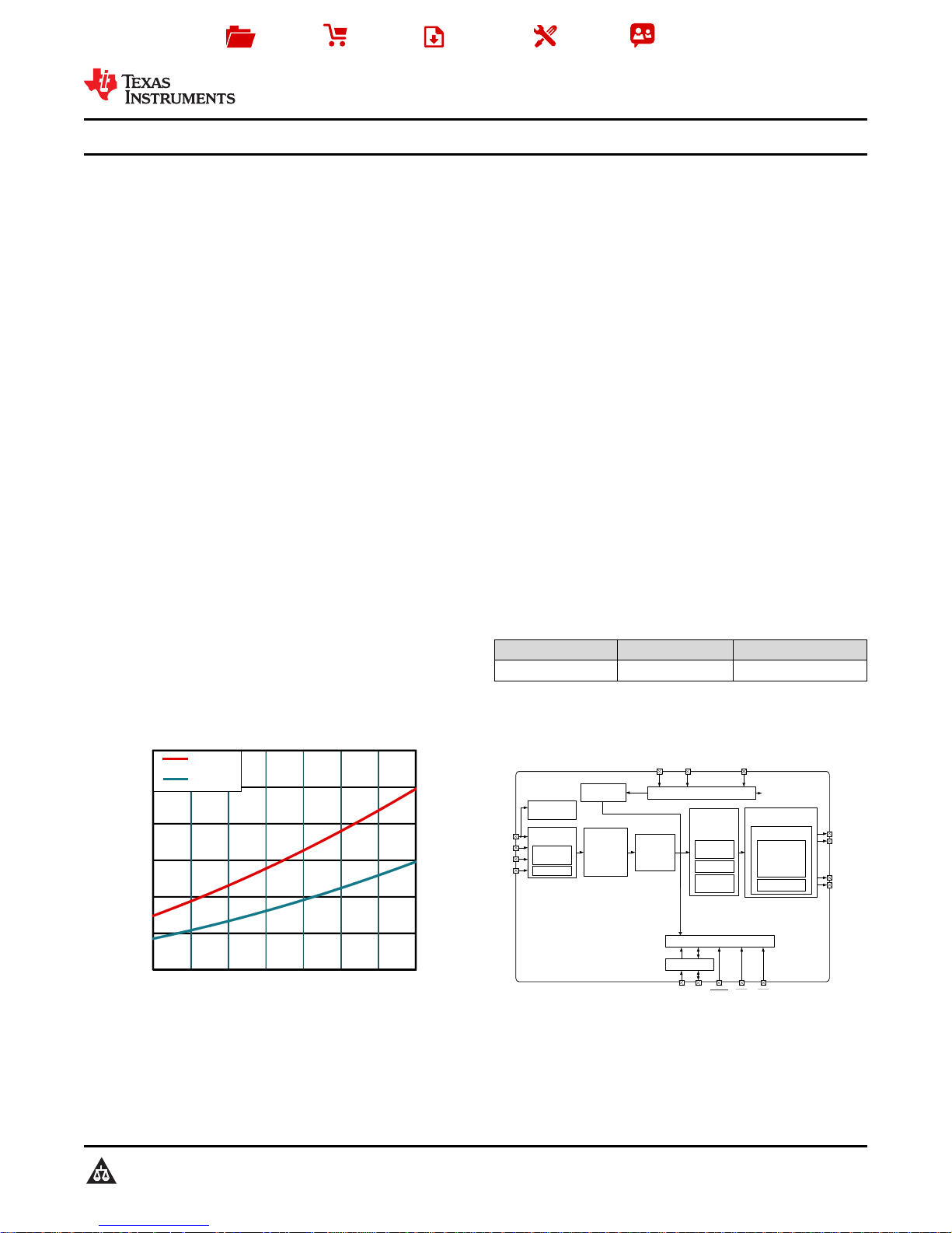
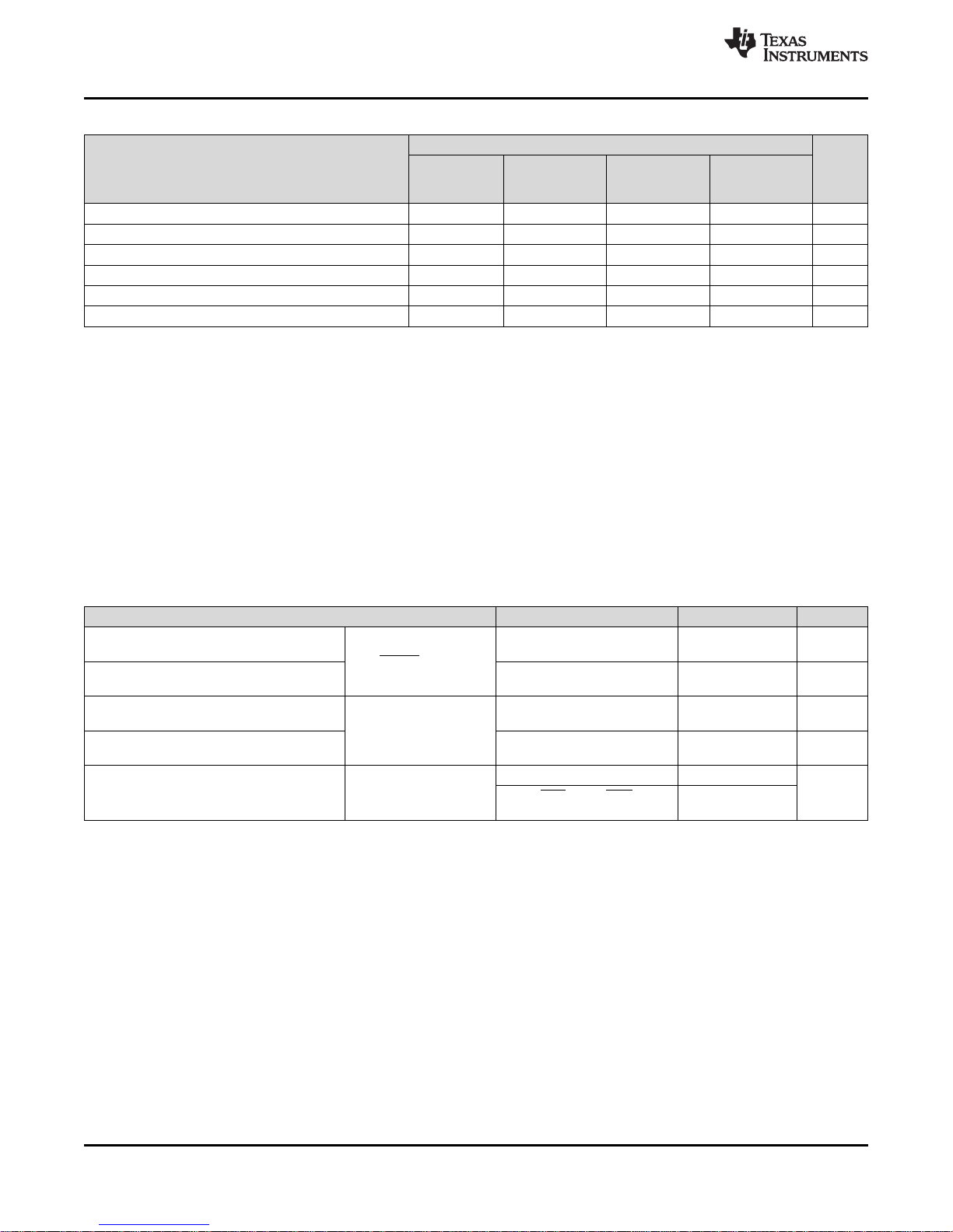
Output Power (W)
PVDD (V)
RL = 4 Ω
RL = 8 Ω
Digital Audio
Processor
(DAP)
Sample Rate
Converter
(SRC)
I²C Control Port
Internal Register/State Machine Interfac e
Power-On Reset
(POR)
PVDDDVDD
MCLK Monitoring
and Watchdog
AVDD
PDN RST
AMP_OUT_A
AMP_OUT_C
SDIN
MCLK
SCLK
LRCK
SCL SDA
Serial Audio Port
(SAP)
Sample Rate
Auto-Detect
PLL
Digital to PWM
Converter
(DPC)
Click & Pop
Suppression
2 Ch. PWM
Modulator
Noise Shaping
Open Loop Stereo
Stereo PWM Amplifier
Sensing & Protection
Temperature
Short Circuits
PVDD Voltage
Output Current
Fault Notification
Internal Voltage Supplies
Internal Regulation and Power Distribution
AMP_OUT_B
AMP_OUT_D
DR_SD
Product
Folder
Sample &
Buy
Technical
Documents
Tools &
Software
Support &
Community
TAS5733L
SLASE77A –MARCH 2016–REVISED MARCH 2016
TAS5733L - Digital Input Audio Power Amplifier with EQ and 3-Band AGL
1 Features
1
• Audio Input/Output
– One-Stereo Serial Audio Input
– Supports 44.1-kHz and 48-kHz Sample Rates
(LJ/RJ/I²S)
– Supports 3-Wire I²S Mode (no MCLK required)
– Automatic Audio Port Rate Detection
– Supports BTL and PBTL Configuration
– P
• Audio/PWM Processing
– Independent Channel Volume Controls With
– Programmable Three-Band Automatic Gain
– 20 Programmable Biquads for Speaker EQ
• General Features
– 104-dB SNR, A-Weighted, Referenced to Full
– I²C Serial Control Interface w/ two Addresses
– Thermal, Short-Circuit, and Undervoltage
– Up to 90% Efficient
– AD, BD, and Ternary Modulation
– PWM Level Meter
= 10 W @ 10% THD+N
OUT
– PVDD = 12 V, 8 Ω, 1 kHz
Gain of 24 dB to Mute in 0.125-dB Steps
Limiting (AGL)
and Other Audio-Processing Features
Scale (0 dB)
Protection
Power vs PVDD
2 Applications
• LCD TV, LED TV
• Low-Cost Audio Equipment
3 Description
The TAS5733L device is an efficient, digital-input
audio amplifier for driving stereo speakers configured
as a bridge tied load (BTL). In parallel bridge tied
load (PBTL) in can produce higher power by driving
the parallel outputs into a single lower impedance
load. One serial data input allows processing of up to
two discrete audio channels and seamless integration
to most digital audio processors and MPEG
decoders. The device accepts a wide range of input
data and data rates. A fully programmable data path
routes these channels to the internal speaker drivers.
The TAS5733L device is a slave-only device
receiving all clocks from external sources. The
TAS5733L device operates with a PWM carrier
between a 384-kHz switching rate and a 288-kHz
switching rate, depending on the input sample rate.
Oversampling combined with a fourth-order noise
shaper provides a flat noise floor and excellent
dynamic range from 20 Hz to 20 kHz.
Device Information
PART NUMBER PACKAGE BODY SIZE (NOM)
TAS5733L HTSSOP (48) 12.50 mm × 6.10 mm
(1) For all available packages, see the orderable addendum at
the end of the data sheet.
Simplified Block Diagram
(1)
1
An IMPORTANT NOTICE at the end of this data sheet addresses availability, warranty, changes, use in safety-critical applications,
intellectual property matters and other important disclaimers. PRODUCTION DATA.
Page 2

TAS5733L
SLASE77A –MARCH 2016–REVISED MARCH 2016
www.ti.com
Table of Contents
1 Features.................................................................. 1
2 Applications ........................................................... 1
3 Description ............................................................. 1
4 Revision History..................................................... 2
5 Pin Configuration and Functions......................... 3
6 Specifications......................................................... 5
6.1 Absolute Maximum Ratings ...................................... 5
6.2 ESD Ratings ............................................................ 5
6.3 Recommended Operating Conditions....................... 5
6.4 Thermal Characteristics............................................ 6
6.5 Electrical Characteristics........................................... 6
6.6 Speaker Amplifier Characteristics............................. 7
6.7 Protection Characteristics......................................... 7
6.8 Master Clock Characteristics .................................... 7
6.9 I²C Interface Timing Requirements........................... 8
6.10 Serial Audio Port Timing Requirements.................. 8
6.11 Typical Characteristics - Stereo BTL Mode .......... 11
6.12 Typical Characteristics - Mono PBTL Mode ......... 13
7 Detailed Description............................................ 15
7.1 Overview................................................................. 15
7.2 Functional Block Diagram....................................... 15
7.3 Audio Signal Processing Overview......................... 16
7.4 Feature Description................................................. 17
7.5 Device Functional Modes........................................ 19
7.6 Programming........................................................... 20
7.7 Register Maps......................................................... 31
8 Application and Implementation ........................ 49
8.1 Application Information............................................ 49
8.2 Typical Applications ............................................... 50
9 Power Supply Recommendations...................... 55
10 Layout................................................................... 56
10.1 Layout Guidelines ................................................. 56
10.2 Layout Example .................................................... 57
11 Device and Documentation Support................. 59
11.1 Trademarks........................................................... 59
11.2 Electrostatic Discharge Caution............................ 59
11.3 Glossary................................................................ 59
12 Mechanical, Packaging, and Orderable
Information........................................................... 60
4 Revision History
NOTE: Page numbers for previous revisions may differ from page numbers in the current version.
Changes from Original (March 2016) to Revision A Page
• Moved from Product Preview to Production Data release. ................................................................................................... 1
2
Submit Documentation Feedback Copyright © 2016, Texas Instruments Incorporated
Product Folder Links: TAS5733L
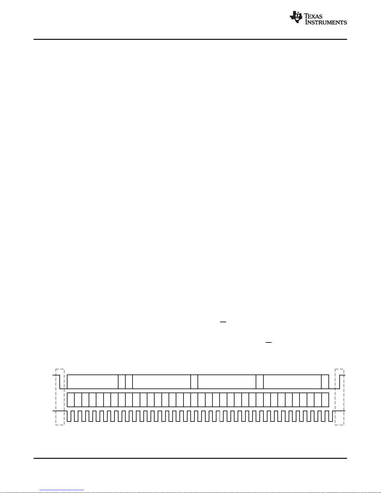
Page 3
PowerPAD
TM
1
2
3
4
5
6
7
8
9
10
11
12
13
14
15
16
17
18
19
20
21
22
23
24
48
47
46
45
44
43
42
41
40
39
38
37
36
35
34
33
32
31
30
29
28
27
26
25
BSTRP_B
AMP_OUT _B
AMP_OUT _B
PGND
PGND
AMP_OUT _A
PVDD
PVDD
BSTRP_A
SSTIMER
PBTL
NC
NC
PLL_GND
PLL_FLTM
PLL_FLTP
AVDD_REF
AVDD
ADR / FAULT
MCLK
OSC_RES
OSC _GND
DVDD_REG
PDN
BSTRP_C
AMP_OUT _C
AMP_OUT _C
PGND
PGND
AMP_OUT _D
PVDD
PVDD
BSTRP_D
GVDD_REG
AVDD_REG
NC
NC
AGND
DGND
DVDD
TEST
RST
NC
SCL
SDA
SDIN
SCLK
LRCLK
www.ti.com
5 Pin Configuration and Functions
TAS5733L
SLASE77A –MARCH 2016–REVISED MARCH 2016
PIN
NAME NO.
TYPE
ADR/FAULT 19 DI/DO
AGND 35 P
AMP_OUT_A 6
AMP_OUT_B
AMP_OUT_C
2
3
46
47
AMP_OUT_D 43
AVDD 18 P Power supply for internal analog circuitry
AVDD_REF 17 P
AVDD_REG 38 P
BSTRP_A 9
BSTRP_B 1
BSTRP_C 48
BSTRP_D 40
DGND 34 P
DVDD 33 P Power supply for the internal digital circuitry
DVDD_REG 23 P
GVDD_REG 39 P
LRCLK 25 DI
(1) TYPE: A = analog; D = 3.3-V digital; P = power/ground/decoupling; I = input; O = output
48-Pin HTSSOP With PowerPAD™
DCA Package
Top View
Pin Functions
(1)
Dual function terminal which sets the LSB of the I²C Address to 0 if pulled to GND, 1 if
pulled to AVDD. Also, if configured to be a fault output by the methods described in the
Fault Indication section, this terminal will be pulled low when an internal fault occurs.
Ground reference for analog circuitry (NOTE: This terminal should be connected to the
system ground)
AO Speaker amplifier outputs
Internal power supply (NOTE: This terminal is provided as a connection point for filtering
capacitors for this supply and must not be used to power any external circuitry)
Voltage regulator derived from AVDD supply (NOTE: This terminal is provided as a
connection point for filtering capacitors for this supply and must not be used to power
any external circuitry)
P
Connection points to for the bootstrap capacitors, which are used to create a power
supply for the gate drive for the high-side device
Ground reference for digital circuitry (NOTE: This terminal should be connected to the
system ground)
Voltage regulator derived from DVDD supply (NOTE: This terminal is provided as a
connection point for filtering capacitors for this supply and must not be used to power
any external circuitry)
Voltage regulator derived from PVDD supply (NOTE: This terminal is provided as a
connection point for filtering capacitors for this supply and must not be used to power
any external circuitry)
Word select clock for the digital signal that is active on the input data line of the serial
port
Product Folder Links: TAS5733L
DESCRIPTION
Submit Documentation FeedbackCopyright © 2016, Texas Instruments Incorporated
3
Page 4
TAS5733L
SLASE77A –MARCH 2016–REVISED MARCH 2016
www.ti.com
Pin Functions (continued)
PIN
NAME NO.
MCLK 20 DI Master clock used for internal clock tree and sub-circuit/state machine clocking
12
13
(2)
NC
30
36
37
OSC_GND 22 P
OSC_RES 21 AO
PBTL 11 DI
PDN 24 DI Places the device in power down when pulled low
4
PGND
5
44
45
PLL_FLTM 15 AO Negative connection point for the PLL loop filter components
PLL_FLTP 16 AO Positive connection point for the PLL loop filter components
PLL_GND 14 P
7
PVDD
8
41
42
RST 31 DI Places the devices in reset when pulled low
SCL 29 DI I²C serial control port clock
SCLK 26 DI Bit clock for the digital signal that is active on the input data line of the serial data port
SDA 28 DI/DO I²C serial control port data
SDIN 27 DI Data line to the serial data port
SSTIMER 10 AO
TEST 32 —
PowerPAD — P
(2) Although these pins are not connected internally, optimum thermal performance is realized when these pins are connected to the ground
plane. Doing so allows copper on the PCB to fill up to and including these pins, providing a path for heat to conduct away from the
device and into the surrounding PCB area.
(1)
TYPE
P
Not connected inside the device (all "no connect" terminals should be connected to
system ground)
Ground reference for oscillator circuitry (NOTE: These terminals should be connected to
the system ground)
Connection point for precision resistor used by internal oscillator circuit. Details for this
resistor are shown in the Typical Applications section
Places the power stage in BTL mode when pulled low, or in PBTL mode when pulled
high
—
Ground reference for power device circuitry (NOTE: This terminal should be connected
to the system ground)
Ground reference for PLL circuitry (NOTE: This terminal should be connected to the
system ground)
P Power supply for internal power circuitry
Connection point for the capacitor that is used by the ramp timing circuit, as described in
the SSTIMER Pin Functionality section
Used by TI for testing during device production (NOTE: This terminal should be
connected to system ground)
Exposed metal pad on the underside of the device, which serves as an electrical
connection point for ground as well as a heat conduction path from the device into the
board (NOTE: This terminal should be connected to ground through a land pattern
defined in the Mechanical Data section)
DESCRIPTION
4
Submit Documentation Feedback Copyright © 2016, Texas Instruments Incorporated
Product Folder Links: TAS5733L
Page 5
TAS5733L
www.ti.com
SLASE77A –MARCH 2016–REVISED MARCH 2016
6 Specifications
6.1 Absolute Maximum Ratings
over operating free-air temperature range (unless otherwise noted)
Supply voltage
Input voltage
AMP_OUT_x to GND 22
BSTRP_x to GND 29
Operating free-air temperature 0 to 85 °C
Storage temperature range, T
(1) Stresses beyond those listed under Absolute Maximum Ratings may cause permanent damage to the device. These are stress ratings
only and functional operation of the device at these or any other conditions beyond those indicated under Recommended Operating
Conditions is not implied. Exposure to absolute-maximum conditions for extended periods may affect device reliability.
(2) 5-V tolerant inputs are PDN, RST, SCLK, LRCK, MCLK, SDIN, SDA, and SCL.
(3) Maximum pin voltage should not exceed 6 V.
(4) DC voltage + peak ac waveform measured at the pin should be below the allowed limit for all conditions.
DVDD, AVDD –0.3 to 3.6 V
PVDD –0.3 to 20
3.3-V digital input –0.5 to DVDD + 0.5
(2)
digital input (except MCLK) –0.5 to DVDD + 2.5
5-V tolerant MCLK input –0.5 to AVDD + 2.5
stg
6.2 ESD Ratings
Human-body model (HBM), per ANSI/ESDA/JEDEC JS-001
V
(ESD)
(1) JEDEC document JEP155 states that 500-V HBM allows safe manufacturing with a standard ESD control process.
(2) JEDEC document JEP157 states that 250-V CDM allows safe manufacturing with a standard ESD control process.
Electrostatic discharge
Charged-device model (CDM), per JEDEC specification JESD22-
(2)
C101
(1)
VALUE UNIT
(3)
(3)
(4)
(4)
V5-V tolerant
V
V
–40 to 125 °C
VALUE UNIT
(1)
±4000
±1500
V
6.3 Recommended Operating Conditions
MIN NOM MAX UNIT
DVDD, AVDD Digital, analog supply voltage 3 3.3 3.6 V
PVDD Output power devices supply voltage 8 16.5
V
IH
V
IL
T
A
(2)
T
J
R
L
R
L
L
O
High-level input voltage 5-V tolerant 2 V
Low-level input voltage 5-V tolerant 0.8 V
Operating ambient temperature range 0 85 °C
Operating junction temperature range 0 125 °C
Load impedance 4 8 Ω
Load impedance in PBTL 2 Ω
Output-filter inductance
Minimum output inductance under
short-circuit condition
10 μH
(1) For operation at PVDD levels greater than 14.5 V, the modulation limit must be set to 96.1% or lower via the control port register 0x10.
(2) 16.5 V is the maximum recommended voltage for continuous operation of the TAS5733L device. Testing and characterization of the
device is performed up to and including 16.5 V to ensure “in system” design margin. However, continuous operation at these levels is
not recommended. Operation above the maximum recommended voltage may result in reduced performance, errant operation, and
reduction in device reliability.
(1)
(2)
V
Product Folder Links: TAS5733L
Submit Documentation FeedbackCopyright © 2016, Texas Instruments Incorporated
5
Page 6
TAS5733L
SLASE77A –MARCH 2016–REVISED MARCH 2016
www.ti.com
6.4 Thermal Characteristics
DCA (48 PINS)
THERMAL METRIC
(1)
Special Test
Case
θ
θ
θ
ψ
ψ
θ
Junction-to-ambient thermal resistance
JA
Junction-to-case (top) thermal resistance
JCtop
Junction-to-board thermal resistance
JB
Junction-to-top characterization parameter
JT
Junction-to-board characterization parameter
JB
Junction-to-case (bottom) thermal resistance
JCbot
(2)
(3)
(4)
(5)
(6)
(7)
14.9 16.7 °C/W
6.9 7.9 °C/W
1.7 2.2 °C/W
(1) For more information about traditional and new thermal metrics, see the Semiconductor and IC Package Thermal Metrics application
report (SPRA953).
(2) The junction-to-ambient thermal resistance under natural convection is obtained in a simulation on a JEDEC-standard, high-K board, as
specified in JESD51-7, in an environment described in JESD51-2a.
(3) The junction-to-case (top) thermal resistance is obtained by simulating a cold plate test on the package top. No specific JEDEC-
standard test exists, but a close description can be found in the ANSI SEMI standard G30-88.
(4) The junction-to-board thermal resistance is obtained by simulating in an environment with a ring cold plate fixture to control the PCB
temperature, as described in JESD51-8.
(5) The junction-to-top characterization parameter, ψJT, estimates the junction temperature of a device in a real system and is extracted
from the simulation data for obtaining R
(6) The junction-to-board characterization parameter, ψJB, estimates the junction temperature of a device in a real system and is extracted
from the simulation data for obtaining R
(7) The junction-to-case (bottom) thermal resistance is obtained by simulating a cold plate test on the exposed (power) pad. No specific
, using a procedure described in JESD51-2a (sections 6 and 7).
θJA
, using a procedure described in JESD51-2a (sections 6 and 7).
θJA
JEDEC standard test exists, but a close description can be found in the ANSI SEMI standard G30-88.
Spacer
JEDEC
Standard 2-
Layer PCB
JEDEC
Standard 4-
Layer PCB
TAS5733LEVM
50.7 27.6 25.0 °C/W
1.2 0.8 0.7 °C/W
11.8 7.8 5.8 °C/W
UNITS
6.5 Electrical Characteristics
TA= 25°, PVDD_x = 12 V, DVDD = AVDD = 3.3 V, RL= 8 Ω, BTL BD mode, fS= 48 kHz (unless otherwise noted)
PARAMETER TEST CONDITIONS MIN TYP MAX UNIT
V
OH
High-level output voltage
ADR/FAULT and SDA
V
OL
I
IL
Low-level output voltage
Low-level input current
Digital Inputs
I
IH
I
DD
High-level input current
3.3-V supply current
3.3-V supply voltage
(DVDD, AVDD)
IOH= –4 mA
DVDD = AVDD = 3 V
IOL= 4 mA
DVDD = AVDD = 3 V
VI< V
IL
DVDD = AVDD = 3.6 V
VI> V
IH
DVDD = AVDD = 3.6 V
2.4 V
0.5 V
Normal mode 49 68
Reset (RST = low, PDN =
high)
23 38
75 μA
75 μA
mA
6
Submit Documentation Feedback Copyright © 2016, Texas Instruments Incorporated
Product Folder Links: TAS5733L
Page 7
TAS5733L
www.ti.com
SLASE77A –MARCH 2016–REVISED MARCH 2016
6.6 Speaker Amplifier Characteristics
PVDD = 12 V, BTL BD mode, AVDD = DVDD = 3.3 V, fS= 48 KHz, RL= 8 Ω, audio frequency = 1 kHz, AES17 filter, f
384 kHz, TA= 25°C (unless otherwise specified). All performance is in accordance with recommended operating conditions
and as tested on the TAS5733L EVM.
PARAMETER TEST CONDITIONS MIN TYP MAX UNIT
PVDD = 12 V, 10% THD, 1-kHz input signal 10
PVDD = 12 V, 7% THD, 1-kHz input signal 9
P
O
THD+N
V
n
Power output per channel
Total harmonic distortion +
noise
Output integrated noise (rms) A-weighted 30 μV
Crosstalk
Output switching frequency
I
PVDD
Supply current No load (PVDD)
Drain-to-source resistance,
DS(on)
Drain-to-source resistance,
low side
(1)
r
high side
R
PD
Internal pulldown resistor at
the output of each half-bridge
(1) This does not include bond-wire or pin resistance.
PVDD = 12 V, 1% THD, 1-kHz input signal 7.5
PVDD = 13.2 V, 10% THD, 1-kHz input signal 12
PVDD = 13.2 V, 7% THD, 1-kHz input signal 11
PVDD = 13.2 V, 1% THD, 1-kHz input signal 9
PVDD = 12 V, PO= 1 W 0.25
PVDD = 13.2 V, PO= 1 W 0.3
PO= 1 W, f = 1 kHz (BD Mode), PVDD = 12 V –79 dB
PO=1 W, f = 1 kHz (AD Mode), PVDD = 12 V –62 dB
11.025, 22.05, 44.1-kHz data rate ±2% 288
48, 24, 12, 8, 16, 32-kHz data rate ±2% 384
Normal mode 16 25
Reset (RST = low, PDN = high) 3 8
TJ= 25°C, includes metallization resistance 120
TJ= 25°C, includes metallization resistance 120
Connected when drivers are in the high-impedance
state to provide bootstrap capacitor charge.
3 kΩ
PWM
W
%
kHz
mA
mΩ
=
6.7 Protection Characteristics
TA= 25°, PVDD_x = 12 V, DVDD = AVDD = 3.3 V, RL= 8 Ω, BTL BD mode, fS= 48 kHz (unless otherwise noted)
PARAMETER TEST CONDITIONS MIN TYP MAX UNIT
V
uvp(fall)
V
uvp(rise)
OTE Overtemperature error 150 °C
I
OC
I
OCT
6.8 Master Clock Characteristics
PVDD = 12 V, BTL BD mode, AVDD = DVDD = 3.3 V, fS= 48 kHz, RL= 8 Ω, audio frequency = 1 kHz, AES17 filter, f
384 kHz, TA= 25°C (unless otherwise specified). All performance is in accordance with recommended operating conditions
(unless otherwise specified).
PLL INPUT PARAMETERS
f
MCLKI
tr/ t
f(MCLK)
(1) For clocks related to the serial audio port, please see Serial Audio Port Timing Requirements.
Undervoltage protection limit PVDD falling 5.4 V
Undervoltage protection limit PVDD rising 5.8 V
Overcurrent limit protection 4 A
Overcurrent response time 150 ns
(1)
PWM
PARAMETER TEST CONDITIONS MIN TYP MAX UNIT
MCLK frequency 2.8224 24.576 MHz
MCLK duty cycle 40% 50% 60%
Rise/fall time for MCLK 5 ns
=
Product Folder Links: TAS5733L
Submit Documentation FeedbackCopyright © 2016, Texas Instruments Incorporated
7
Page 8
TAS5733L
SLASE77A –MARCH 2016–REVISED MARCH 2016
6.9 I²C Interface Timing Requirements
t
w(RST)
t
d(I²C_ready)
f
SCL
t
w(H)
t
w(L)
t
r
t
f
t
su1
t
h1
t
(buf)
t
su2
t
h2
t
su3
C
L
Pulse duration, RST active 100 μs
Time to enable I²C after RST goes high 13.5 ms
Frequency, SCL 400 kHz
Pulse duration, SCL high 0.6 μs
Pulse duration, SCL low 1.3 μs
Rise time, SCL and SDA 300 ns
Fall time, SCL and SDA 300 ns
Setup time, SDA to SCL 100 ns
Hold time, SCL to SDA 0 ns
Bus free time between stop and start conditions 1.3 μs
Setup time, SCL to start condition 0.6 μs
Hold time, start condition to SCL 0.6 μs
Setup time, SCL to stop condition 0.6 μs
Load capacitance for each bus line 400 pF
6.10 Serial Audio Port Timing Requirements
over recommended operating conditions (unless otherwise noted)
PARAMETER TEST CONDITIONS MIN TYP MAX UNIT
f
SCLKIN
t
su1
t
h1
t
su2
t
h2
t
(edge)
tr/t
f
Frequency, SCLK 32 × fS, 48 × fS, 64 × f
S
Setup time, LRCK to SCLK rising edge 10 ns
Hold time, LRCK from SCLK rising edge 10 ns
Setup time, SDIN to SCLK rising edge 10 ns
Hold time, SDIN from SCLK rising edge 10 ns
LRCK frequency 8 48 48 kHz
SCLK duty cycle 40% 50% 60%
LRCK duty cycle 40% 50% 60%
SCLK rising edges between LRCK rising edges 32 64
LRCK clock edge with respect to the falling edge of SCLK –1/4 1/4
Rise/fall time for SCLK/LRCK 8 ns
LRCK allowable drift before LRCK reset 4 MCLKs
MIN NOM MAX UNIT
CL≤ 30 pF 1.024 12.28
www.ti.com
MHz
8
SCLK
edges
SCLK
period
8
Submit Documentation Feedback Copyright © 2016, Texas Instruments Incorporated
Product Folder Links: TAS5733L
Page 9
SCL
SDA
t
h2
t
(buf)
t
su2
t
su3
Start
Condition
Stop
Condition
T0028-01
SCL
SDA
t
w(H)
t
w(L)
t
r
t
f
t
su1
t
h1
T0027-01
t
w(RST)
RST
t
d(I2C_ready)
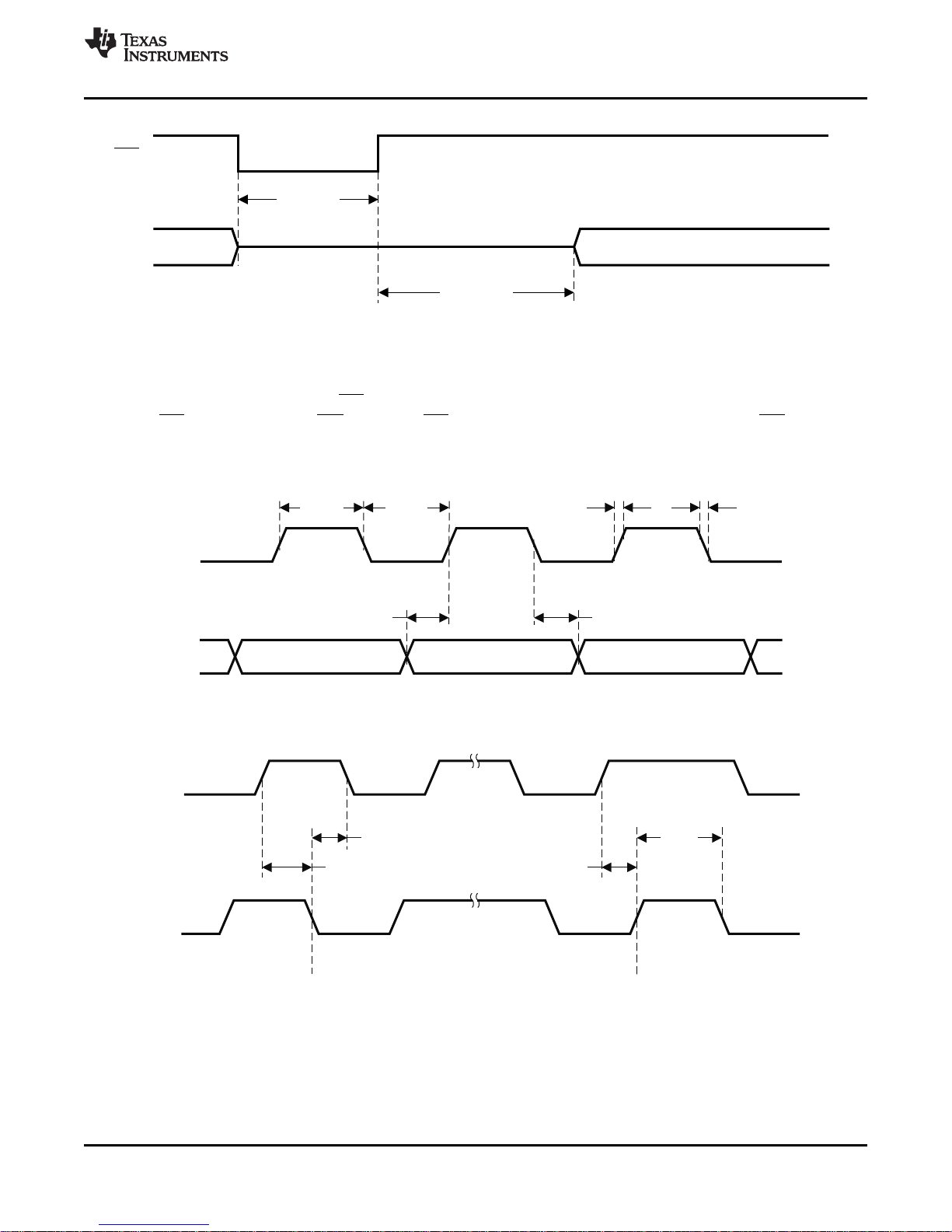
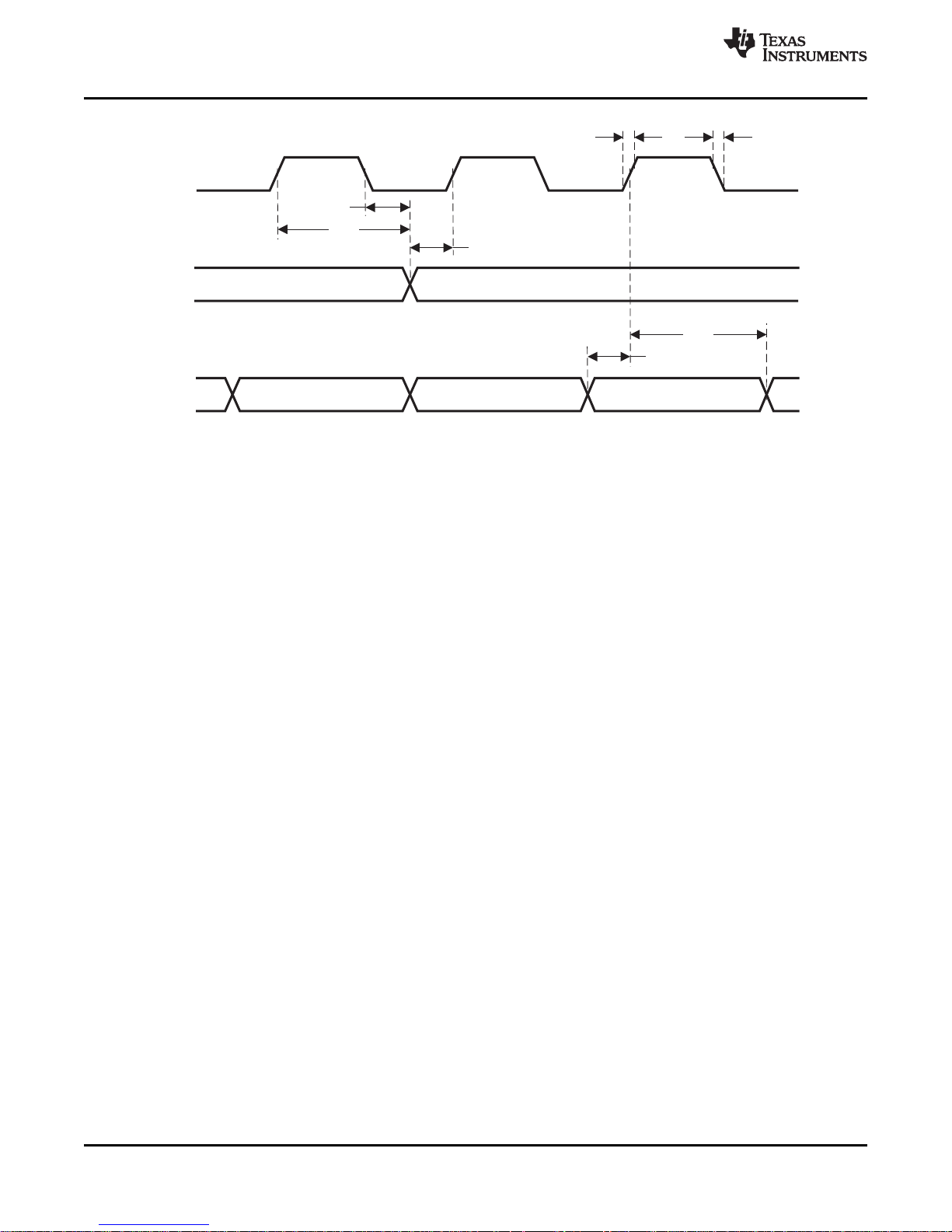
System Initialization.
Enable via I C.
2
T0421-01
I C Active
2
I C Active
2
www.ti.com
SLASE77A –MARCH 2016–REVISED MARCH 2016
NOTE: On power up, hold the TAS5733L RST LOW for at least 100 μs after DVDD has reached 3 V.
NOTE: If RST is asserted LOW while PDN is LOW, then RST must continue to be held LOW for at least 100 μs after PDN is
deasserted (HIGH).
Figure 1. Reset Timing
TAS5733L
Figure 2. SCL and SDA Timing
Figure 3. Start and Stop Conditions Timing
Product Folder Links: TAS5733L
Submit Documentation FeedbackCopyright © 2016, Texas Instruments Incorporated
9
Page 10
t
h1
t
su1
t
(edge)
t
su2
t
h2
SCLK
(Input)
LRCLK
(Input)
SDIN
T0026-04
t
r
t
f
TAS5733L
SLASE77A –MARCH 2016–REVISED MARCH 2016
www.ti.com
Figure 4. Serial Audio Port Timing
10
Submit Documentation Feedback Copyright © 2016, Texas Instruments Incorporated
Product Folder Links: TAS5733L
Page 11
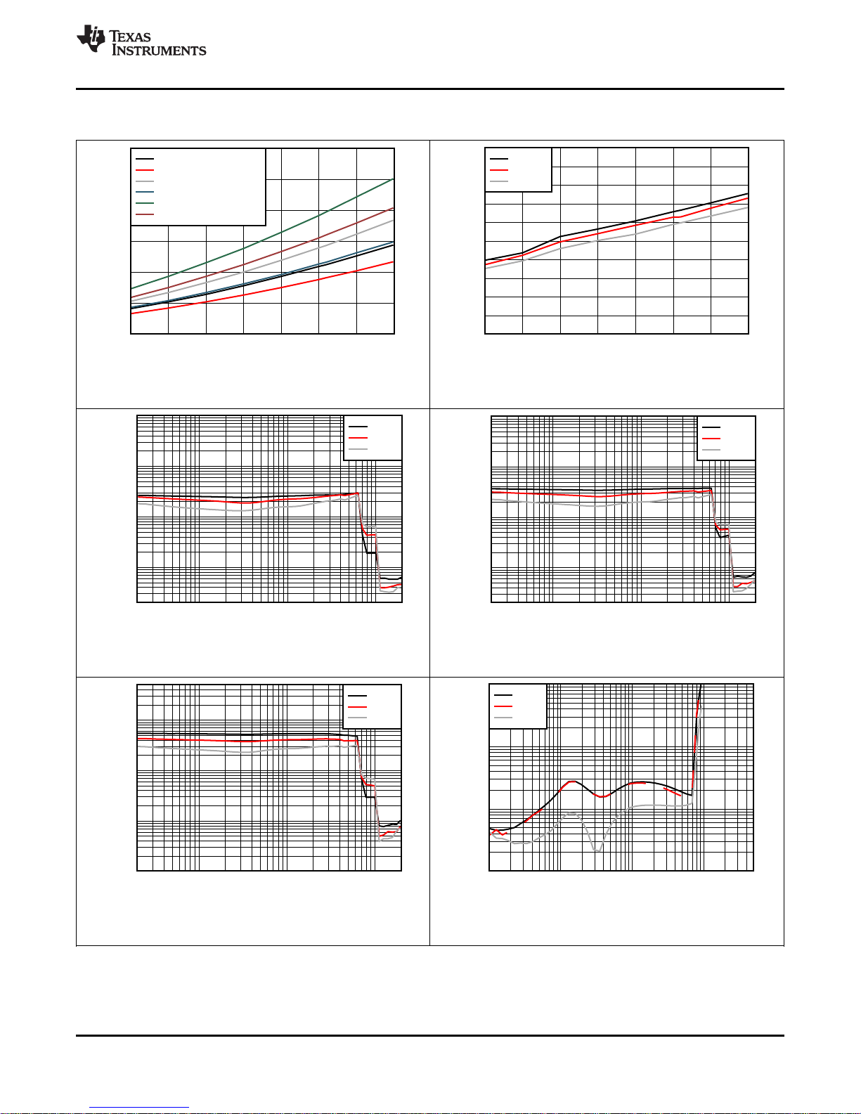
Frequency (Hz)
THD+N (%)
0.001
0.01
0.1
1
55
20 100 1k 10k 20k
D003
1 W
2.5 W
5 W
Output Power (W)
THD+N (%)
0.01 0.1 1 10 50
0.01
0.1
1
10
D001
20 Hz
1 kHz
7 kHz
Frequency (Hz)
THD+N (%)
0.002
0.01
0.1
1
10
20 100 1k 10k 20k
D001
1 W
2.5 W
5 W
Frequency (Hz)
THD+N (%)
0.002
0.01
0.1
1
10
10 100 1k 10k 20k
D002
1 W
2.5 W
5 W
PVDD (V)
Output Power (W)
8 9 10 11 12 13 14 15
0
5
10
15
20
25
30
D007
THD+N = 10%; 8 Ohms
THD+N = 1%; 8 Ohms
THD+N = 10%; 6 Ohms
THD+N = 1%; 6 Ohms
THD+N = 10%; 4 Ohms
THD+N = 1%; 4 Ohms
PVDD (V)
Idle Channel Noise (µV)
8 9 10 11 12 13 14 15
0
5
10
15
20
25
30
35
40
45
50
D012
8 Ohms
6 Ohms
4 Ohms
www.ti.com
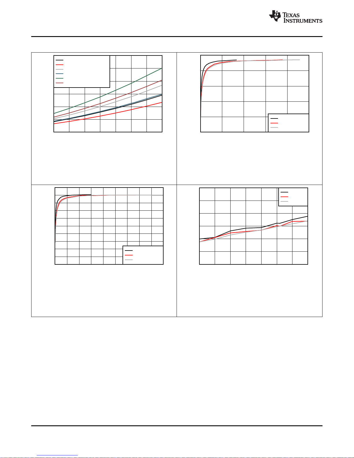
6.11 Typical Characteristics - Stereo BTL Mode
Figure 5. Output Power vs Supply Voltage - BTL Figure 6. Idle Channel Noise vs Supply Voltage - BTL
TAS5733L
SLASE77A –MARCH 2016–REVISED MARCH 2016
PVDD = 12 V RL= 8 Ω
Figure 7. THD+N vs Frequency - BTL
PVDD = 12 V RL= 4 Ω
Figure 9. THD+N vs Frequency - BTL
PVDD = 12 V RL= 6 Ω
PVDD = 12 V RL= 8 Ω
Product Folder Links: TAS5733L
Figure 8. THD+N vs Frequency - BTL
Figure 10. THD+N vs Output Power - BTL
Submit Documentation FeedbackCopyright © 2016, Texas Instruments Incorporated
11
Page 12
Frequency (Hz)
Crosstalk (dB)
-100
-90
-80
-70
-60
-50
-40
-30
-20
-10
0
20 100 1k 10k 20k
D010
Right to Left
Left to Right
Frequency (Hz)
Crosstalk (dB)
-100
-90
-80
-70
-60
-50
-40
-30
-20
-10
0
20 100 1k 10k 20k
D011
Right to Left
Left to Right
Total Output Power (W)
Efficiency (%)
0 5 10 15 20 25
0
10
20
30
40
50
60
70
80
90
100
D008
PVDD = 8 V
PVDD = 12 V
PVDD = 13.2 V
Output Power (W)
Efficiency (%)
0 5 10 15 20 25 30 35 40 45 50
0
10
20
30
40
50
60
70
80
90
100
D009
PVDD = 8 V
PVDD = 12 V
PVDD = 13.2 V
Output Power (W)
THD+N (%)
0.01 0.1 1 10 50
0.001
0.01
0.1
1
10
2020
D001
20 Hz
1 kHz
7 kHz
Output Power (W)
THD+N (%)
0.01 0.1 1 10 50
0.01
0.1
1
10
D006
20 Hz
1 kHz
7 kHz
TAS5733L
SLASE77A –MARCH 2016–REVISED MARCH 2016
Typical Characteristics - Stereo BTL Mode (continued)
www.ti.com
PVDD = 12 V RL= 6 Ω
Figure 11. THD+N vs Output Power - BTL
RL= 8 Ω
Total Output Power includes power delivered from both amplifier
outputs. For instance, 40 W of total output power means 2 × 20 W,
with 20 W delivered by one channel and 20 W delivered by the
other channel.
Figure 13. Efficiency vs Total Output Power - BTL
PVDD = 12 V RL= 4 Ω
Figure 12. THD+N vs Output Power - BTL
RL= 4 Ω
Total Output Power includes power delivered from both amplifier
outputs. For instance, 40 W of total output power means 2 × 20 W,
with 20 W delivered by one channel and 20 W delivered by the
other channel.
Figure 14. Efficiency vs Total Output Power - BTL
PVDD = 12 V RL= 8 Ω
Figure 15. Crosstalk vs Frequency - BTL
12
Submit Documentation Feedback Copyright © 2016, Texas Instruments Incorporated
PVDD = 12 V RL= 4 Ω
Figure 16. Crosstalk vs Frequency - BTL
Product Folder Links: TAS5733L
Page 13
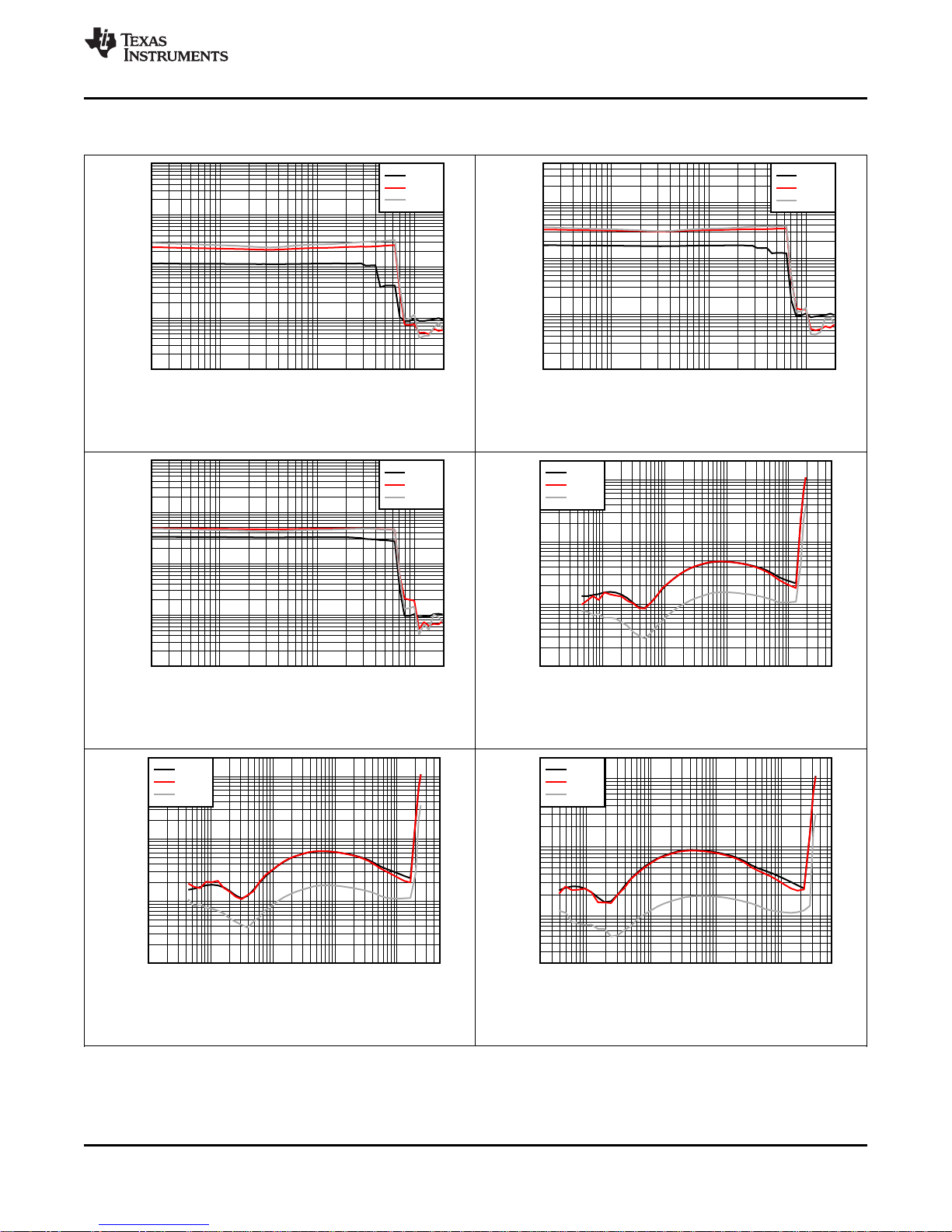
Output Power (W)
THD+N (%)
0.001 0.01 0.1 1 10 50
0.01
0.1
1
10
2020
D017
20 Hz
1 kHz
7 kHz
Output Power (W)
THD+N (%)
0.002 0.01 0.1 1 10 6060
0.02
0.1
1
10
2020
D018
20 Hz
1 kHz
7 kHz
Frequency (Hz)
THD+N (%)
0.001
0.01
0.1
1
10
20 100 1k 10k 20k
D015
1 W
2.5 W
5 W
Output Power (W)
THD+N (%)
0.001 0.01 0.1 1 10 50
0.01
0.1
1
10
2020
D016
20 Hz
1 kHz
7 kHz
Frequency (Hz)
THD+N (%)
0.001
0.01
0.1
1
10
20 100 1k 10k 20k
D013
1 W
2.5 W
5 W
Frequency (Hz)
THD+N (%)
0.001
0.01
0.1
1
55
20 100 1k 10k 20k
D014
1 W
2.5 W
5 W
www.ti.com
6.12 Typical Characteristics - Mono PBTL Mode
TAS5733L
SLASE77A –MARCH 2016–REVISED MARCH 2016
PVDD = 12 V RL= 4 Ω
Figure 17. THD+N vs Frequency - PBTL
PVDD = 12 V RL= 2 Ω
Figure 19. THD+N vs Frequency - PBTL
PVDD = 12 V RL= 3 Ω
Figure 18. THD+N vs Frequency - PBTL
PVDD = 12 V RL= 4 Ω
Figure 20. THD+N vs Output Power - PBTL
PVDD = 12 V RL= 3 Ω
Figure 21. THD+N vs Output Power - PBTL
PVDD = 12 V RL= 2 Ω
Product Folder Links: TAS5733L
Figure 22. THD+N vs Output Power - PBTL
Submit Documentation FeedbackCopyright © 2016, Texas Instruments Incorporated
13
Page 14
Output Power (W)
Efficiency (%)
0 5 10 15 20 25 30 35 40 45
0
10
20
30
40
50
60
70
80
90
100
D021
PVDD = 8 V
PVDD = 12 V
PVDD = 13.2 V
PVDD (V)
Idle Channel Noise (µV)
8 9 10 11 12 13 14 15
0
10
20
30
40
50
60
D022
RL = 4 R
RL = 3 R
RL = 2 R
Supply Voltage (V)
Output Power (W)
8 9 10 11 12 13 14 15
0
10
20
30
40
50
60
D019
THD+N = 10%; RL = 4R
THD+N = 1%; RL = 4R
THD+N = 10%; RL = 3R
THD+N = 1%; RL = 3R
THD+N = 10%; RL = 2R
THD+N = 1%; RL = 2R
Output Power (W)
Efficiency (%)
0 5 10 15 20 25
0
20
40
60
80
100
D020
PVDD = 8 V
PVDD = 12 V
PVDD = 13.2 V
TAS5733L
SLASE77A –MARCH 2016–REVISED MARCH 2016
Typical Characteristics - Mono PBTL Mode (continued)
Figure 23. Output Power vs PVDD - PBTL
Total Output Power includes power delivered from both amplifier
outputs. For instance, 40 W of total output power means 2 × 20 W,
with 20 W delivered by one channel and 20 W delivered by the
www.ti.com
RL= 4 Ω
other channel.
Figure 24. Efficiency vs Output Power - PBTL
RL= 2 Ω
Total Output Power includes power delivered from both amplifier
outputs. For instance, 40 W of total output power means 2 × 20 W,
with 20 W delivered by one channel and 20 W delivered by the
other channel.
Figure 25. Efficiency vs Output Power - PBTL
14
Submit Documentation Feedback Copyright © 2016, Texas Instruments Incorporated
Figure 26. Idle Channel Noise vs PVDD - PBTL
Product Folder Links: TAS5733L
Page 15
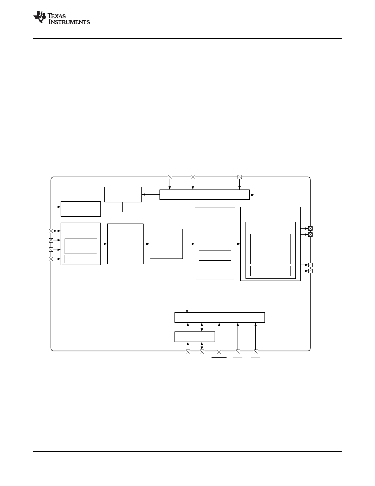
Digital Audio
Processor
(DAP)
Sample Rate
Converter
(SRC)
I²C Control Port
Internal Register/State Machine Interface
Power-On Reset
(POR)
PVDDDVDD
MCLK Monitoring
and Watchdog
AVDD
PDN RST
AMP_OUT_A
AMP_OUT_C
SDIN
MCLK
SCLK
LRCK
SCL SDA
Serial Audio Port
(SAP)
Sample Rate
Auto-Detect
PLL
Digital to PWM
Converter
(DPC)
Click & Pop
Suppression
2 Ch. PWM
Modulator
Noise Shaping
Open Loop Stereo
Stereo PWM Amplifier
Sensing & Protection
Temperature
Short Circuits
PVDD Voltage
Output Current
Fault Notification
Internal Voltage Supplies
Internal Regulation and Power Distribution
AMP_OUT_B
AMP_OUT_D
DR_SD
TAS5733L
www.ti.com
SLASE77A –MARCH 2016–REVISED MARCH 2016
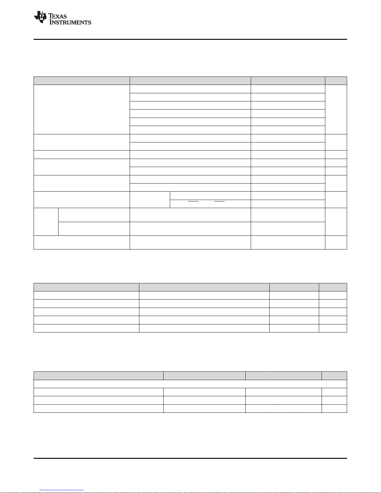
7 Detailed Description
7.1 Overview
The TAS5733L device is an efficient, digital-input audio amplifier for driving stereo speakers configured as a
bridge tied load (BTL). In parallel bridge tied load (PBTL) in can produce higher power by driving the parallel
outputs into a single lower impedance load. One serial data input allows processing of up to two discrete audio
channels and seamless integration to most digital audio processors and MPEG decoders. The device accepts a
wide range of input data and data rates. A fully programmable data path routes these channels to the internal
speaker drivers.
The TAS5733L device is a slave-only device receiving all clocks from external sources. The TAS5733L device
operates with a PWM carrier between a 384-kHz switching rate and a 288-kHz switching rate, depending on the
input sample rate. Oversampling combined with a fourth-order noise shaper provides a flat noise floor and
excellent dynamic range from 20 Hz to 20 kHz.
7.2 Functional Block Diagram
Figure 27. TAS5733L Functional Block Diagram
Product Folder Links: TAS5733L
Submit Documentation FeedbackCopyright © 2016, Texas Instruments Incorporated
15
Page 16
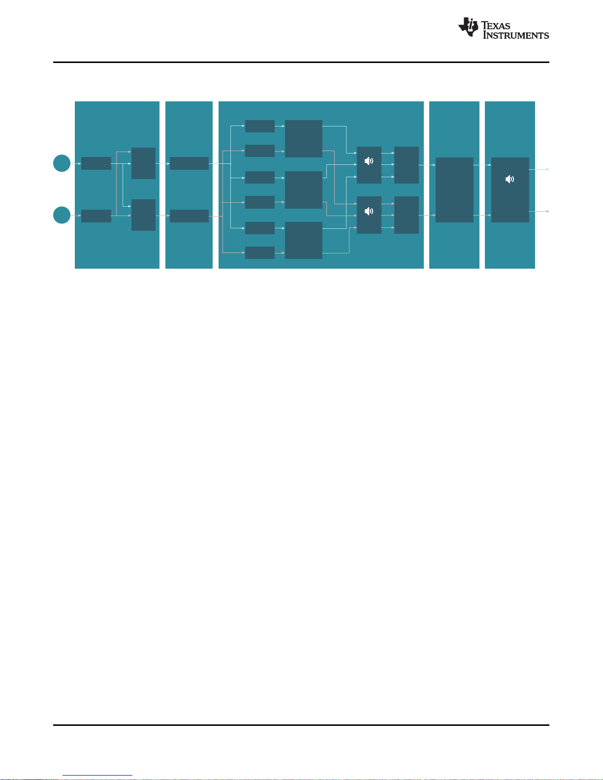
L
R
Input
Mixer L
AGL 1
Low Band
Vol 1
Vol 2
Mixer L
AGL 4
Full Band
Mixer R
AGL 2
High Band
AGL 3
Mid Band
10 Biquads
Biquad
Biquad
2 Biquads
2 Biquads
Biquad
Biquad
10 Biquads
Biquad
0x26
0x59
0x8
0x9
0x51
0x52
0x5E
0x5A
0x5F
0x5B, 0x5C
0x60, 0x61
0x76, 0x77
0x72, 0x73
0x27 - 0x2F, 0x58
0x3B - 0x3C, 0x40
0x3E - 0x3F, 0x43
0x44 - 0x45, 0x48
0x42 - 0x41, 0x47
0x31 - 0x39, 0x5D
0x30
DC Bloc k and L R Mixer Equalize r Mu lti Ban d AGL Full Ba nd AGL
L
R
Master Volume,
Pre Scale,
Post Scale
0x07 - 0x57, 0x56
Master Volume
Biquad
Input
Mixer R
TAS5733L
SLASE77A –MARCH 2016–REVISED MARCH 2016
7.3 Audio Signal Processing Overview
Figure 28. TAS5733L Audio Process Flow
www.ti.com
16
Submit Documentation Feedback Copyright © 2016, Texas Instruments Incorporated
Product Folder Links: TAS5733L
Page 17
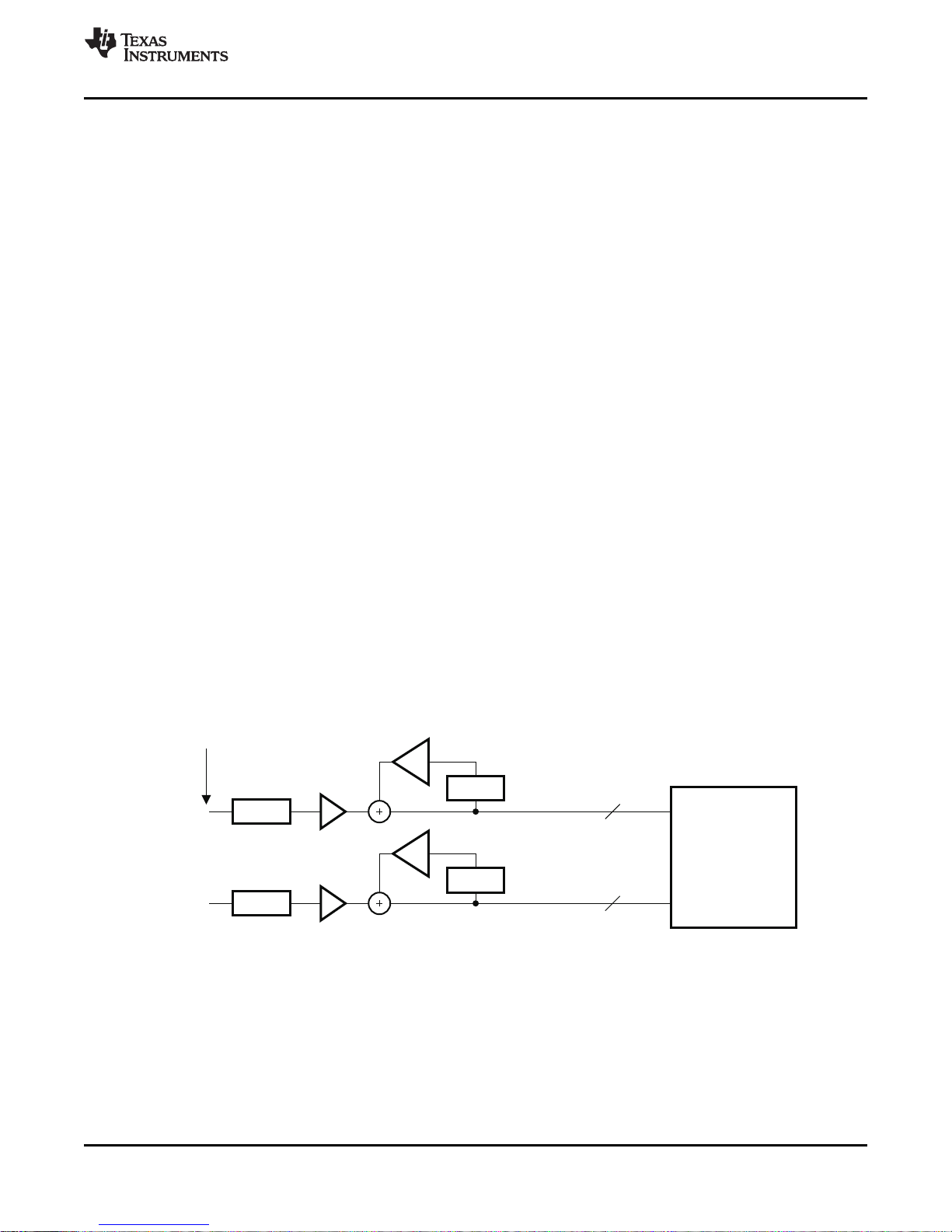
B0396-01
1 – a
rms
ABSCh1
Z
–1
a
Post-DAP Processing
32-BitLevel
I CRegisters
(PWMLevelMeter)
2
rms
ABSCh2
Z
–1
32-BitLevel
ADDR=0x6C
ADDR=0x6B
1 – a
a
TAS5733L
www.ti.com
SLASE77A –MARCH 2016–REVISED MARCH 2016
7.4 Feature Description
7.4.1 Clock, Autodetection, and PLL
The TAS5733L device is an I²S slave device. The TAS5733L device accepts MCLK, SCLK, and LRCK. The
digital audio processor (DAP) supports all the sample rates and MCLK rates that are defined in the Clock Control
Register.
The TAS5733L device checks to verify that SCLK is a specific value of 32 fS, 48 fS, or 64 fS. The DAP only
supports a 1 × fSLRCK. The timing relationship of these clocks to SDIN is shown in subsequent sections. The
clock section uses MCLK or the internal oscillator clock (when MCLK is unstable, out of range, or absent) to
produce the internal clock (DCLK) running at 512 times the PWM switching frequency.
The DAP can autodetect and set the internal clock control logic to the appropriate settings for all supported clock
rates as defined in the Clock Control Register.
The TAS5733L device has robust clock error handling that uses the built-in trimmed oscillator clock to quickly
detect changes/errors. Once the system detects a clock change/error, the system mutes the audio (through a
single-step mute) and then forces PLL to limp using the internal oscillator as a reference clock. Once the clocks
are stable, the system autodetects the new rate and reverts to normal operation. During this process, the default
volume is restored in a single step (also called hard unmute). The ramp process can be programmed to ramp
back slowly (also called soft unmute) as defined in the Volume Configuration Register.
7.4.2 PWM Section
The TAS5733L DAP device uses noise-shaping and customized nonlinear correction algorithms to achieve high
power efficiency and high-performance digital audio reproduction. The DAP uses a fourth-order noise shaper to
increase dynamic range and SNR in the audio band. The PWM section accepts 24-bit PCM data from the DAP
and outputs two BTL PWM audio output channels.
The PWM section has individual-channel dc-blocking filters that can be enabled and disabled. The filter cutoff
frequency is less than 1 Hz.
The PWM section has an adjustable maximum modulation limit of 93.8% to 99.2%. For PVDD > 14.5 V the
modulation index must be limited to 96.1% for safe and reliable operation.
7.4.3 PWM Level Meter
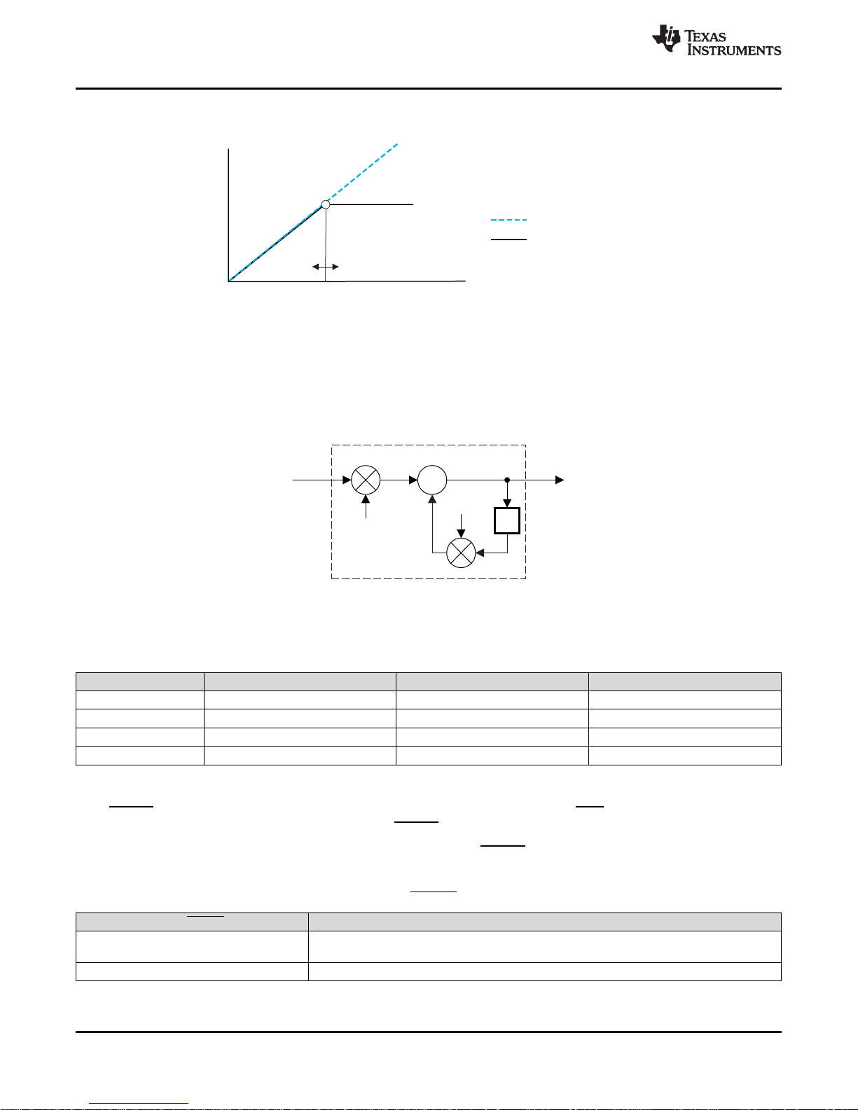
The structure in Figure 29 shows the PWM level meter that can be used to study the power profile.
7.4.4 Automatic Gain Limiter (AGL)
The AGL scheme has three AGL blocks. One ganged AGL exists for the high-band left/right channels, the midband left/right channels, and the low-band left/right channels.
The AGL input/output diagram is shown in Figure 30.
Figure 29. PWM Level Meter Structure
Product Folder Links: TAS5733L
Submit Documentation FeedbackCopyright © 2016, Texas Instruments Incorporated
17
Page 18
S
Z
–1
Alpha Filter Structure
w
a
Output Level (dB)
Input Level (dB)
T
M0091-04
1:1 TransferFunction
Implemented TransferFunction
TAS5733L
SLASE77A –MARCH 2016–REVISED MARCH 2016
Feature Description (continued)
Professional-quality dynamic range compression automatically adjusts volume to flatten volume level.
• Each AGL has adjustable threshold levels.
• Programmable attack and decay time constants
• Transparent compression: compressors can attack fast enough to avoid apparent clipping before engaging,
and decay times can be set slow enough to avoid pumping.
www.ti.com
Figure 30. Automatic Gain Limiter
T = 9.23 format, all other AGL coefficients are 3.23 format
Figure 31. AGL Structure
Table 1. AGL Structure
α, ω T αa, ωa / αd, ωd
AGL 1 0x3B 0x40 0x3C
AGL 2 0x3E 0x43 0x3F
AGL 3 0x47 0x41 0x42
AGL 4 0x48 0x44 0x45
7.4.5 Fault Indication
ADR/FAULT is an input pin during power up. This pin can be programmed after RST to be an output by writing 1
to bit 0 of I²C register 0x05. In that mode, the ADR/FAULT pin has the definition shown in Table 2.
Any fault resulting in device shutdown is signaled by the ADR/FAULT pin going low (see Table 2). A latched
version of this pin is available on D1 of register 0x02. This bit can be reset only by an I²C write.
Table 2. ADR/FAULT Output States
ADR/FAULT DESCRIPTION
0 Overcurrent (OC) or undervoltage (UVP) error or overtemperature error (OTE) or overvoltage
1 No faults (normal operation)
error
18
Submit Documentation Feedback Copyright © 2016, Texas Instruments Incorporated
Product Folder Links: TAS5733L
Page 19

TAS5733L
www.ti.com
SLASE77A –MARCH 2016–REVISED MARCH 2016
7.4.6 SSTIMER Pin Functionality
The SSTIMER pin uses a capacitor connected between this pin and ground to control the output duty cycle when
exiting all-channel shutdown. The capacitor on the SSTIMER pin is slowly charged through an internal current
source, and the charge time determines the rate at which the output transitions from a near-zero duty cycle to the
desired duty cycle. This allows for a smooth transition that minimizes audible pops and clicks. When the part is
shut down, the drivers are placed in the high-impedance state and transition slowly down through an internal 3kΩ resistor, similarly minimizing pops and clicks. The shutdown transition time is independent of the SSTIMER
pin capacitance. Larger capacitors increase the start-up time, while smaller capacitors decrease the start-up
time. The SSTIMER pin can be left floating for BD modulation.
7.4.7 Device Protection System
7.4.7.1 Overcurrent (OC) Protection With Current Limiting
The TAS5733L device has independent, fast-reacting current detectors on all high-side and low-side power-stage
FETs. The detector outputs are closely monitored to prevent the output current from increasing beyond the
overcurrent threshold defined in the Protection Characteristics table.
If the output current increases beyond the overcurrent threshold, the device shuts down and the outputs
transition to the off or high impedance (Hi-Z) state. The device returns to normal operation once the fault
condition (i.e., a short circuit on the output) is removed. Current-limiting and overcurrent protection are not
independent for half-bridges. That is, if the bridge-tied load between half-bridges A and B causes an overcurrent
fault, half-bridges A, B, C, and D shut down.
7.4.7.2 Overtemperature Protection
The TAS5733L device has an overtemperature-protection system. If the device junction temperature exceeds
150°C (nominal), the device enters thermal shutdown, where all half-bridge outputs enter the high-impedance
(Hi-Z) state, and ADR/FAULT asserts low if the device is configured to function as a fault output. The TAS5733L
device recovers automatically once the junction temperature of the device drops approximately 30°C.
7.4.7.3 Undervoltage Protection (UVP) and Power-On Reset (POR)
The UVP and POR circuits of the TAS5733L device fully protect the device in any power-up/down and brownout
situation. While powering up, the POR circuit resets the overload circuit (OLP) and ensures that all circuits are
fully operational when the PVDD and AVDD supply voltages reach 7.6 V and 2.7 V, respectively. Although PVDD
and AVDD are independently monitored. For PVDD, if the supply voltage drops below the UVP threshold, the
protection feature immediately sets all half-bridge outputs to the high-impedance (Hi-Z) state and asserts
ADR/FAULT low.
7.5 Device Functional Modes
The TAS5733L device is a digital input class-d amplifier with audio processing capabilities. The TAS5733L
device has numerous modes to configure and control the device.
7.5.1 Serial Audio Port Operating Modes
The serial audio port in the TAS5733L device supports industry-standard audio data formats, including I²S, Leftjustified(LJ) and Right-justified(RJ) formats. To select the data format that will be used with the device can
controlled by using the serial data interface registers 0x04. The default is 24bit, I²S mode. The timing diagrams
for the various serial audio port are shown in the Serial Interface Control and Timing section
7.5.2 Communication Port Operating Modes
The TAS5733L device is configured via an I²C communication port. The I²C communication protocol is detailed in
the 7.7 I²C Serial Control Port Requirements and Specifications section.
Product Folder Links: TAS5733L
Submit Documentation FeedbackCopyright © 2016, Texas Instruments Incorporated
19
Page 20
7-BitSlave Address
R/
W
8-BitRegister Address(N)
A
8-BitRegisterDataFor
Address(N)
Start Stop
SDA
SCL
7
6
5
4
3
2 1
0
7
6
5
4
3
2 1
0
7
6
5
4
3
2 1
0
7
6
5
4
3
2 1
0
A
8-BitRegisterDataFor
Address(N)
A A
T0035-01
TAS5733L
SLASE77A –MARCH 2016–REVISED MARCH 2016
www.ti.com
Device Functional Modes (continued)
7.5.3 Speaker Amplifier Modes
The TAS5733L device can be configured as:
• Stereo Mode
• Mono Mode
7.5.3.1 Stereo Mode
Stereo mode is the most common option for the TAS5733L. TAS5733L can be connected in 2.0 mode to drive
stereo channels. Detailed application section regarding the stereo mode is discussed in the Stereo Bridge Tied
Load Application section.
7.5.3.2 Mono Mode
Mono mode is described as the operation where the two BTL outputs of amplifier are placed in parallel with one
another to provide increase in the output power capability. This mode is typically used to drive subwoofers, which
require more power to drive larger loudspeakers with high-amplitude, low-frequency energy. Detailed application
section regarding the mono mode is discussed in the Mono Parallel Bridge Tied Load Application section.
7.6 Programming
7.6.1 I²C Serial Control Interface
The TAS5733L device has a bidirectional I²C interface that is compatible with the Inter IC (I²C) bus protocol and
supports both 100-kHz and 400-kHz data transfer rates for single- and multiple-byte write and read operations.
This is a slave-only device that does not support a multimaster bus environment or wait-state insertion. The
control interface is used to program the registers of the device and to read device status.
The DAP supports the standard-mode I²C bus operation (100 kHz maximum) and the fast I²C bus operation
(400 kHz maximum). The DAP performs all I²C operations without I²C wait cycles.
7.6.1.1 General I²C Operation
The I²C bus employs two signals, SDA (data) and SCL (clock), to communicate between integrated circuits in a
system. Data is transferred on the bus serially, one bit at a time. The address and data can be transferred in byte
(8-bit) format, with the most-significant bit (MSB) transferred first. In addition, each byte transferred on the bus is
acknowledged by the receiving device with an acknowledge bit. Each transfer operation begins with the master
device driving a start condition on the bus and ends with the master device driving a stop condition on the bus.
The bus uses transitions on the data pin (SDA) while the clock is high to indicate start and stop conditions. A
high-to-low transition on SDA indicates a start and a low-to-high transition indicates a stop. Normal data-bit
transitions must occur within the low time of the clock period. These conditions are shown in Figure 32. The
master generates the 7-bit slave address and the read/write (R/W) bit to open communication with another
device and then waits for an acknowledge condition. The TAS5733L device holds SDA low during the
acknowledge clock period to indicate an acknowledgment. When this occurs, the master transmits the next byte
of the sequence. Each device is addressed by a unique 7-bit slave address plus R/W bit (1 byte). All compatible
devices share the same signals via a bidirectional bus using a wired-AND connection. An external pullup resistor
must be used for the SDA and SCL signals to set the high level for the bus.
20
Submit Documentation Feedback Copyright © 2016, Texas Instruments Incorporated
Figure 32. Typical I²C Sequence
Product Folder Links: TAS5733L
Page 21

TAS5733L
www.ti.com
SLASE77A –MARCH 2016–REVISED MARCH 2016
Programming (continued)
No limit exists for the number of bytes that can be transmitted between start and stop conditions. When the last
word transfers, the master generates a stop condition to release the bus. A generic data transfer sequence is
shown in Figure 32.
The 7-bit address for the TAS5733L device is 0101 010 (0x54) or 0101 011 (0x56) as defined by ADR/FAULT
(external pulldown for 0x54 and pullup for 0x56).
7.6.1.2 I²C Slave Address
The ADR/FAULT is an input pin during power-up and after each toggle of RST, which is used to set the I²C subaddress of the device. The ADR/FAULT can also operate as a fault output after power-up is complete and the
address has been latched in.
At power-up, and after each toggle of RST, the pin is read to determine its voltage level. If the pin is left floating,
an internal pull-up will set the I²C sub-address to 0x56. This will also be the case if an external resistor is used to
pull the pin up to AVDD. To set the sub-address to 0x54, an external resistor (specified in Typical Applications )
must be connected to the system ground.
As mentioned, the pin can also be reconfigured as an output driver via I²C for fault monitoring. Use System
Control Register 2 (0x05) to set ADR/FAULT pin to be used as a fault output during fault conditions.
I²C Device Address Change Procedure
1. Write to device address change enable register, 0xF8 with a value of 0xF9A5 A5A5.
2. Write to device register 0xF9 with a value of 0x0000 00XX, where XX is the new address.
3. Any writes after that should use the new device address XX.
7.6.1.3 Single- and Multiple-Byte Transfers
The serial control interface supports both single-byte and multiple-byte read/write operations for subaddresses
0x00 to 0x1F. However, for the subaddresses 0x20 to 0xFF, the serial control interface supports only multiplebyte read/write operations (in multiples of 4 bytes).
During multiple-byte read operations, the DAP responds with data, a byte at a time, starting at the subaddress
assigned, as long as the master device continues to respond with acknowledges. If a particular subaddress does
not contain 32 bits, the unused bits are read as logic 0.
During multiple-byte write operations, the DAP compares the number of bytes transmitted to the number of bytes
that are required for each specific subaddress. For example, if a write command is received for a biquad
subaddress, the DAP must receive five 32-bit words. If fewer than five 32-bit data words have been received
when a stop command (or another start command) is received, the received data is discarded.
Supplying a subaddress for each subaddress transaction is referred to as random I²C addressing. The
TAS5733L device also supports sequential I²C addressing. For write transactions, if a subaddress is issued
followed by data for that subaddress and the 15 subaddresses that follow, a sequential I²C write transaction has
taken place, and the data for all 16 subaddresses is successfully received by the TAS5733L device. For I²C
sequential-write transactions, the subaddress then serves as the start address, and the amount of data
subsequently transmitted before a stop or start is transmitted determines how many subaddresses are written.
As was true for random addressing, sequential addressing requires that a complete set of data be transmitted. If
only a partial set of data is written to the last subaddress, the data for the last subaddress is discarded. However,
all other data written is accepted; only the incomplete data is discarded.
Product Folder Links: TAS5733L
Submit Documentation FeedbackCopyright © 2016, Texas Instruments Incorporated
21
Page 22

D7 D0 ACK
Stop
Condition
Acknowledge
I CDevice Addressand
2
Read/WriteBit
Subaddress LastDataByte
A6 A5 A1 A0 R/W ACK A7 A5 A1 A0 ACK D7 ACK
Start
Condition
Acknowledge Acknowledge Acknowledge
FirstDataByte
A4 A3A6
OtherDataBytes
ACK
Acknowledge
D0 D7 D0
T0036-02
A6 A5 A4 A3 A2 A1 A0
R/W
ACK A7 A6 A5 A4 A3 A2 A1 A0 ACK D7 D6 D5 D4 D3 D2 D1 D0 ACK
Start
Condition
Stop
Condition
Acknowledge Acknowledge Acknowledge
I CDevice Addressand
2
Read/WriteBit
Subaddress DataByte
T0036-01
TAS5733L
SLASE77A –MARCH 2016–REVISED MARCH 2016
www.ti.com
Programming (continued)
7.6.1.4 Single-Byte Write
As shown in Figure 33, a single-byte data-write transfer begins with the master device transmitting a start
condition followed by the I²C device address and the read/write bit. The read/write bit determines the direction of
the data transfer. For a data-write transfer, the read/write bit is a 0. After receiving the correct I²C device address
and the read/write bit, the DAP responds with an acknowledge bit. Next, the master transmits the address byte or
bytes corresponding to the internal memory address being accessed. After receiving the address byte, the
TAS5733L device again responds with an acknowledge bit. Next, the master device transmits the data byte to be
written to the memory address being accessed. After receiving the data byte, the TAS5733L device again
responds with an acknowledge bit. Finally, the master device transmits a stop condition to complete the singlebyte data-write transfer.
Figure 33. Single-Byte Write Transfer
7.6.1.5 Multiple-Byte Write
A multiple-byte data-write transfer is identical to a single-byte data-write transfer except that multiple data bytes
are transmitted by the master device to the DAP as shown in Figure 34. After receiving each data byte, the
TAS5733L device responds with an acknowledge bit.
Figure 34. Multiple-Byte Write Transfer
7.6.1.6 Single-Byte Read
As shown in Figure 35, a single-byte data-read transfer begins with the master device transmitting a start
condition, followed by the I²C device address and the read/write bit. For the data read transfer, both a write
followed by a read are actually done. Initially, a write is done to transfer the address byte or bytes of the internal
memory address to be read. As a result, the read/write bit becomes a 0. After receiving the TAS5733L address
and the read/write bit, TAS5733L device responds with an acknowledge bit. In addition, after sending the internal
memory address byte or bytes, the master device transmits another start condition followed by the TAS5733L
address and the read/write bit again. This time, the read/write bit becomes a 1, indicating a read transfer. After
receiving the address and the read/write bit, the TAS5733L device again responds with an acknowledge bit.
Next, the TAS5733L device transmits the data byte from the memory address being read. After receiving the
data byte, the master device transmits a not-acknowledge followed by a stop condition to complete the singlebyte data-read transfer.
22
Submit Documentation Feedback Copyright © 2016, Texas Instruments Incorporated
Product Folder Links: TAS5733L
Page 23

A6 A0 ACK
Acknowledge
I CDevice Addressand
Read/WriteBit
2
R/WA6 A0 R/W ACK A0 ACK D7 D0 ACK
Start
Condition
Stop
Condition
Acknowledge Acknowledge Acknowledge
LastDataByte
ACK
FirstDataByte
RepeatStart
Condition
Not
Acknowledge
I CDevice Addressand
Read/WriteBit
2
Subaddress OtherDataBytes
A7 A6 A5 D7 D0 ACK
Acknowledge
D7 D0
T0036-04
A6 A5 A0 R/W ACK A7 A6 A5 A4 A0 ACK A6 A5 A0 ACK
Start
Condition
Stop
Condition
Acknowledge Acknowledge Acknowledge
I CDevice Addressand
2
Read/WriteBit
Subaddress DataByte
D7 D6 D1 D0 ACK
I CDevice Addressand
Read/WriteBit
2
Not
Acknowledge
R/WA1 A1
RepeatStart
Condition
T0036-03
TAS5733L
www.ti.com
SLASE77A –MARCH 2016–REVISED MARCH 2016
Programming (continued)
Figure 35. Single-Byte Read Transfer
7.6.1.7 Multiple-Byte Read
A multiple-byte data-read transfer is identical to a single-byte data-read transfer except that multiple data bytes
are transmitted by the TAS5733L device to the master device as shown in Figure 36. Except for the last data
byte, the master device responds with an acknowledge bit after receiving each data byte.
Figure 36. Multiple-Byte Read Transfer
7.6.2 Serial Interface Control and Timing
7.6.2.1 Serial Data Interface
Serial data is input on SDIN. The PWM outputs are derived from SDIN. The TAS5733L DAP accepts serial data
in 16-bit, 20-bit, or 24-bit left-justified, right-justified, and I²S serial data formats.
7.6.2.2 I²S Timing
I²S timing uses LRCK to define when the data being transmitted is for the left channel and when the data is for
the right channel. LRCK is low for the left channel and high for the right channel. A bit clock running at 32 × fS,
48 × fS, or 64 × fSis used to clock in the data. A delay of one bit clock exists from the time the LRCK signal
changes state to the first bit of data on the data lines. The data is written MSB-first and is valid on the rising edge
of bit clock. The DAP masks unused trailing data bit positions.
Product Folder Links: TAS5733L
Submit Documentation FeedbackCopyright © 2016, Texas Instruments Incorporated
23
Page 24

23
22
SCLK
32Clks
LRCLK(NoteReversedPhase)
LeftChannel
24-BitMode
1
19 18
20-BitMode
16-BitMode
15
14
MSB LSB
32Clks
RightChannel
2-ChannelI S(PhilipsFormat)StereoInput
2
T0034-01
5
4
9 8
1
0
0
4
5
1
0
23
22 1
19 18
15
14
MSB LSB
5
4
9 8
1
0
0
4
5
1
0
SCLK
TAS5733L
SLASE77A –MARCH 2016–REVISED MARCH 2016
Programming (continued)
www.ti.com
NOTE: All data presented in two's-complement form with MSB first.
Figure 37. I²S 64-fSFormat
24
Submit Documentation Feedback Copyright © 2016, Texas Instruments Incorporated
Product Folder Links: TAS5733L
Page 25

SCLK
16Clks
LRCLK
LeftChannel
16-BitMode
1 1
15 15
14 14
MSB LSB
16Clks
RightChannel
2-ChannelI S(PhilipsFormat)StereoInput
2
T0266-01
3 3
2 2
5 5
4 4
9 98 80
13 13
10 10
11 1112 12
SCLK
MSB LSB
23
22
SCLK
24Clks
LRCLK
LeftChannel
24-BitMode
1
19 18
20-BitMode
16-BitMode
15
14
MSB LSB
24Clks
RightChannel
2-ChannelI S(PhilipsFormat)StereoInput/Output(24-Bit TransferWordSize)
2
T0092-01
3
2
5
4
9 8
17
16
1
0
0
4
5
13
12
1
09 8
23
22
SCLK
1
19 18
15
14
MSB LSB
3
2
5
4
9 8
17
16
1
0
4
5
13
12
1
09 8
www.ti.com
Programming (continued)
TAS5733L
SLASE77A –MARCH 2016–REVISED MARCH 2016
NOTE: All data presented in two's-complement form with MSB first.
Figure 38. I²S 48-fSFormat
NOTE: All data presented in two's-complement form with MSB first.
Figure 39. I²S 32-fSFormat
Submit Documentation FeedbackCopyright © 2016, Texas Instruments Incorporated
Product Folder Links: TAS5733L
25
Page 26

23
22
SCLK
32Clks
LRCLK
LeftChannel
24-BitMode
1
19 18
20-BitMode
16-BitMode
15
14
MSB LSB
32Clks
RightChannel
2-ChannelLeft-JustifiedStereoInput
T0034-02
4
5
9 8
1
4
5
1
0
0
0
23
22 1
19 18
15
14
MSB LSB
4
5
9 8
1
4
5
1
0
0
0
SCLK
TAS5733L
SLASE77A –MARCH 2016–REVISED MARCH 2016
www.ti.com
Programming (continued)
7.6.2.3 Left-Justified
Left-justified (LJ) timing uses LRCK to define when the data being transmitted is for the left channel and when
the data is for the right channel. LRCK is high for the left channel and low for the right channel. A bit clock
running at 32 × fS, 48 × fS, or 64 × fSis used to clock in the data. The first bit of data appears on the data lines at
the same time LRCK toggles. The data is written MSB-first and is valid on the rising edge of the bit clock. The
DAP masks unused trailing data bit positions.
NOTE: All data presented in two's-complement form with MSB first.
Figure 40. Left-Justified 64-fSFormat
26
Submit Documentation Feedback Copyright © 2016, Texas Instruments Incorporated
Product Folder Links: TAS5733L
Page 27

SCLK
16Clks
LRCLK
LeftChannel
16-BitMode
1 1
15 15
14 14
MSB LSB
16Clks
RightChannel
2-ChannelLeft-JustifiedStereoInput
T0266-02
3 3
2 2
5 5
4 4
9 98 80 0
13 13
10 10
11 1112 12
SCLK
MSB LSB
23
22
SCLK
24Clks
LRCLK
LeftChannel
24-BitMode
1
19 18
20-BitMode
16-BitMode
15
14
MSB LSB
24Clks
RightChannel
2-ChannelLeft-JustifiedStereoInput(24-Bit TransferWordSize)
T0092-02
4
5
9 8
17
16
1
4
5
13
12
1
9 8
0
0
0
21
17
13
23
22
SCLK
1
19 18
15
14
MSB LSB
4
5
9 8
17
16
1
4
5
13
12
1
9 8
0
0
0
21
17
13
www.ti.com
Programming (continued)
TAS5733L
SLASE77A –MARCH 2016–REVISED MARCH 2016
NOTE: All data presented in two's-complement form with MSB first.
Figure 41. Left-Justified 48-fSFormat
NOTE: All data presented in two's-complement form with MSB first.
Figure 42. Left-Justified 32-fSFormat
Product Folder Links: TAS5733L
Submit Documentation FeedbackCopyright © 2016, Texas Instruments Incorporated
27
Page 28

23
22
SCLK
32Clks
LRCLK
LeftChannel
24-BitMode
1
20-BitMode
16-BitMode
15
14
MSB LSB
SCLK
32Clks
RightChannel
2-ChannelRight-Justified(SonyFormat)StereoInput
T0034-03
19 18
1
19 18
1
0
0
0
15
14
15
14
23
22 1
15
14
MSB LSB
19 18
1
19 18
1
0
0
0
15
14
15
14
TAS5733L
SLASE77A –MARCH 2016–REVISED MARCH 2016
www.ti.com
Programming (continued)
7.6.2.4 Right-Justified
Right-justified (RJ) timing uses LRCK to define when the data being transmitted is for the left channel and when
the data is for the right channel. LRCK is high for the left channel and low for the right channel. A bit clock
running at 32 × fS, 48 × fS, or 64 × fSis used to clock in the data. The first bit of data appears on the data 8 bitclock periods (for 24-bit data) after LRCK toggles. In RJ mode, the LSB of data is always clocked by the last bit
clock before LRCK transitions. The data is written MSB-first and is valid on the rising edge of bit clock. The DAP
masks unused leading data bit positions.
All data presented in two's-complement form with MSB first.
Figure 43. Right-Justified 64-fSFormat
28
Submit Documentation Feedback Copyright © 2016, Texas Instruments Incorporated
Product Folder Links: TAS5733L
Page 29

23
22
SCLK
24Clks
LRCLK
LeftChannel
24-BitMode
1
20-BitMode
16-BitMode
15
14
MSB LSB
SCLK
24Clks
RightChannel
MSB
2-ChannelRight-JustifiedStereoInput(24-Bit TransferWordSize)
T0092-03
5
19 18
1
5
19 18
1
5
0
0
0
2
2
2
6
6
6
15
14
15
14
23
22 1
15
14
5
19 18
1
5
19 18
1
5
0
0
0
2
2
2
6
6
6
15
14
15
14
LSB
www.ti.com
Programming (continued)
TAS5733L
SLASE77A –MARCH 2016–REVISED MARCH 2016
All data presented in two's-complement form with MSB first.
Figure 44. Right-Justified 48-fSFormat
All data presented in two's-complement form with MSB first.
Figure 45. Right-Justified 32-fSFormat
7.6.3 26-Bit 3.23 Number Format
All mixer gain coefficients are 26-bit coefficients using a 3.23 number format. Numbers formatted as 3.23
numbers mean that the binary point has 3 bits to the left and 23 bits to the right. This is shown in Figure 46.
Product Folder Links: TAS5733L
Submit Documentation FeedbackCopyright © 2016, Texas Instruments Incorporated
29
Page 30

u
Coefficient
Digit8
u
u u u u
S
x
Coefficient
Digit7
x.
x x x
Coefficient
Digit6
x
x x x
Coefficient
Digit5
x
x x x
Coefficient
Digit4
x
x x x
Coefficient
Digit3
x
x x x
Coefficient
Digit2
x
x x x
Coefficient
Digit1
Fraction
Digit5
Fraction
Digit4
Fraction
Digit3
Fraction
Digit2
Fraction
Digit1
Integer
Digit1
Sign
Bit
Fraction
Digit6
u=unusedordon’tcarebits
Digit=hexadecimaldigit
M0127-01
0
(1or0) 2 +´1(1or0) 2 +(1or0) 2 +.......(1or0) 2 +.......(1or0) 2´ ´ ´ ´
0 –1 –4 –23
2 Bit
1
2 Bit
0
2 Bit
–1
2 Bit
–4
2 Bit
–23
M0126-01
2 Bit
–23
S_xx.xxxx_xxxx_xxxx_xxxx_xxxx_xxx
2 Bit
–5
2 Bit
–1
2 Bit
0
SignBit
2 Bit
1
M0125-01
TAS5733L
SLASE77A –MARCH 2016–REVISED MARCH 2016
www.ti.com
Programming (continued)
Figure 46. 3.23 Format
The decimal value of a 3.23 format number can be found by following the weighting shown in Figure 46. If the
most significant bit is logic 0, the number is a positive number, and the weighting shown yields the correct
number. If the most significant bit is a logic 1, then the number is a negative number. In the case every bit must
be inverted, a 1 added to the result, and then the weighting shown in Figure 47 applies to obtain the magnitude
of the negative number.
Figure 47. Conversion Weighting Factors—3.23 Format to Floating Point
Gain coefficients, entered via the I²C bus, must be entered as 32-bit binary numbers. The format of the 32-bit
number (4-byte or 8-digit hexadecimal number) is shown in Figure 48.
30
Submit Documentation Feedback Copyright © 2016, Texas Instruments Incorporated
Figure 48. Alignment of 3.23 Coefficient in 32-Bit I²C Word
Product Folder Links: TAS5733L
Page 31

www.ti.com
7.7 Register Maps
7.7.1 Register Summary
SLASE77A –MARCH 2016–REVISED MARCH 2016
Table 3. Sample Calculation for 3.23 Format
db Linear Decimal Hex (3.23 Format)
0 1 8,388,608 800000
5 1.77 14,917,288 00E3 9EA8
–5 0.56 4,717,260 0047 FACC
X L = 10
(X / 20)
D = 8,388,608 × L H = dec2hex (D, 8)
Table 4. Sample Calculation for 9.17 Format
db Linear Decimal Hex (9.17 Format)
0 1 131,072 20000
5 1.77 231,997 3 8A3D
–5 0.56 73,400 1 1EB8
X L = 10
(X / 20)
D = 131,072 × L H = dec2hex (D, 8)
TAS5733L
SUBADDRESS REGISTER NAME
NO. OF
BYTES
CONTENTS
A u indicates unused bits.
0x00 Clock control register 1 Description shown in subsequent section 0x6C
0x01 Device ID register 1 Description shown in subsequent section 0x40
0x02 Error status register 1 Description shown in subsequent section 0x00
0x03 System control register 1 1 Description shown in subsequent section 0xA0
0x04 Serial data interface register 1 Description shown in subsequent section 0x05
0x05 System control register 2 1 Description shown in subsequent section 0x40
0x06 Soft mute register 1 Description shown in subsequent section 0x00
0x07 Master volume 2 Description shown in subsequent section 0x03FF (mute)
0x08 Channel 1 vol 2 Description shown in subsequent section 0x00C0 (0 dB)
0x09 Channel 2 vol 2 Description shown in subsequent section 0x00C0 (0 dB)
0x0A Channel 3 vol 2 Description shown in subsequent section 0x00C0 (0 dB)
0x0B Reserved 2 Reserved
0x0C 2 Reserved
0x0D 1 Reserved
(1)
(1)
(1)
0x0E Volume configuration register 1 Description shown in subsequent section 0xF0
0x0F Reserved 1 Reserved
(1)
0x10 Modulation limit register 1 Description shown in subsequent section 0x01
0x11 IC delay channel 1 1 Description shown in subsequent section 0xAC
0x12 IC delay channel 2 1 Description shown in subsequent section 0x54
0x13 IC delay channel 3 1 Description shown in subsequent section 0xAC
0x14 IC delay channel 4 1 Description shown in subsequent section 0x54
0x15 Reserved 1 Reserved
(1)
0x16 0x54
0x17 0x00
0x18 PWM Start 0x0F
0x19 PWM Shutdown Group Register 1 Description shown in subsequent section 0x30
0x1A Start/stop period register 1 Description shown in subsequent section 0x68
0x1B Oscillator trim register 1 Description shown in subsequent section 0x82
DEFAULT
VALUE
0x03FF
0x00C0
0xC0
0x97
0xAC
(1) Do not access reserved registers.
Product Folder Links: TAS5733L
Submit Documentation FeedbackCopyright © 2016, Texas Instruments Incorporated
31
Page 32
TAS5733L
SLASE77A –MARCH 2016–REVISED MARCH 2016
Register Maps (continued)
www.ti.com
SUBADDRESS REGISTER NAME
NO. OF
BYTES
CONTENTS
0x1C BKND_ERR register 1 Description shown in subsequent section 0x57
0x1D–0x1F 1 Reserved
(1)
0x20 Input MUX register 4 Description shown in subsequent section 0x00017772
0x21 Reserved 4 Reserved
(1)
0x0000 4303
0x22 4 0x0000 0000
0x23 4 0x0000 0000
0x24 4 0x0000 0000
0x25 PWM MUX register 4 Description shown in subsequent section 0x01021345
0x26 ch1_bq[0] 20 u[31:26], b0[25:0] 0x0080 0000
u[31:26], b1[25:0] 0x0000 0000
u[31:26], b2[25:0] 0x0000 0000
u[31:26], a1[25:0] 0x0000 0000
u[31:26], a2[25:0] 0x0000 0000
0x27 ch1_bq[1] 20 u[31:26], b0[25:0] 0x0080 0000
u[31:26], b1[25:0] 0x0000 0000
u[31:26], b2[25:0] 0x0000 0000
u[31:26], a1[25:0] 0x0000 0000
u[31:26], a2[25:0] 0x0000 0000
0x28 ch1_bq[2] 20 u[31:26], b0[25:0] 0x0080 0000
u[31:26], b1[25:0] 0x0000 0000
u[31:26], b2[25:0] 0x0000 0000
u[31:26], a1[25:0] 0x0000 0000
u[31:26], a2[25:0] 0x0000 0000
0x29 ch1_bq[3] 20 u[31:26], b0[25:0] 0x0080 0000
u[31:26], b1[25:0] 0x0000 0000
u[31:26], b2[25:0] 0x0000 0000
u[31:26], a1[25:0] 0x0000 0000
u[31:26], a2[25:0] 0x0000 0000
0x2A ch1_bq[4] 20 u[31:26], b0[25:0] 0x0080 0000
u[31:26], b1[25:0] 0x0000 0000
u[31:26], b2[25:0] 0x0000 0000
u[31:26], a1[25:0] 0x0000 0000
u[31:26], a2[25:0] 0x0000 0000
0x2B ch1_bq[5] 20 u[31:26], b0[25:0] 0x0080 0000
u[31:26], b1[25:0] 0x0000 0000
u[31:26], b2[25:0] 0x0000 0000
u[31:26], a1[25:0] 0x0000 0000
u[31:26], a2[25:0] 0x0000 0000
0x2C ch1_bq[6] 20 u[31:26], b0[25:0] 0x00800000
u[31:26], b1[25:0] 0x0000 0000
u[31:26], b2[25:0] 0x0000 0000
u[31:26], a1[25:0] 0x0000 0000
u[31:26], a2[25:0] 0x0000 0000
DEFAULT
VALUE
0x00
32
Submit Documentation Feedback Copyright © 2016, Texas Instruments Incorporated
Product Folder Links: TAS5733L
Page 33

www.ti.com
Register Maps (continued)
TAS5733L
SLASE77A –MARCH 2016–REVISED MARCH 2016
SUBADDRESS REGISTER NAME
0x2D ch1_bq[7] 20 u[31:26], b0[25:0] 0x00800000
0x2E ch1_bq[8] 20 u[31:26], b0[25:0] 0x0080 0000
0x2F ch1_bq[9] 20 u[31:26], b0[25:0] 0x0080 0000
0x30 ch2_bq[0] 20 u[31:26], b0[25:0] 0x0080 0000
0x31 ch2_bq[1] 20 u[31:26], b0[25:0] 0x0080 0000
0x32 ch2_bq[2] 20 u[31:26], b0[25:0] 0x0080 0000
0x33 ch2_bq[3] 20 u[31:26], b0[25:0] 0x0080 0000
0x34 ch2_bq[4] 20 u[31:26], b0[25:0] 0x0080 0000
0x35 ch2_bq[5] 20 u[31:26], b0[25:0] 0x0080 0000
NO. OF
BYTES
CONTENTS
u[31:26], b1[25:0] 0x0000 0000
u[31:26], b2[25:0] 0x0000 0000
u[31:26], a1[25:0] 0x0000 0000
u[31:26], a2[25:0] 0x0000 0000
u[31:26], b1[25:0] 0x0000 0000
u[31:26], b2[25:0] 0x0000 0000
u[31:26], a1[25:0] 0x0000 0000
u[31:26], a2[25:0] 0x0000 0000
u[31:26], b1[25:0] 0x0000 0000
u[31:26], b2[25:0] 0x0000 0000
u[31:26], a1[25:0] 0x0000 0000
u[31:26], a2[25:0] 0x0000 0000
u[31:26], b1[25:0] 0x0000 0000
u[31:26], b2[25:0] 0x0000 0000
u[31:26], a1[25:0] 0x0000 0000
u[31:26], a2[25:0] 0x0000 0000
u[31:26], b1[25:0] 0x0000 0000
u[31:26], b2[25:0] 0x0000 0000
u[31:26], a1[25:0] 0x0000 0000
u[31:26], a2[25:0] 0x0000 0000
u[31:26], b1[25:0] 0x0000 0000
u[31:26], b2[25:0] 0x0000 0000
u[31:26], a1[25:0] 0x0000 0000
u[31:26], a2[25:0] 0x0000 0000
u[31:26], b1[25:0] 0x0000 0000
u[31:26], b2[25:0] 0x0000 0000
u[31:26], a1[25:0] 0x0000 0000
u[31:26], a2[25:0] 0x0000 0000
u[31:26], b1[25:0] 0x0000 0000
u[31:26], b2[25:0] 0x0000 0000
u[31:26], a1[25:0] 0x0000 0000
u[31:26], a2[25:0] 0x0000 0000
u[31:26], b1[25:0] 0x0000 0000
u[31:26], b2[25:0] 0x0000 0000
u[31:26], a1[25:0] 0x0000 0000
u[31:26], a2[25:0] 0x0000 0000
DEFAULT
VALUE
Product Folder Links: TAS5733L
Submit Documentation FeedbackCopyright © 2016, Texas Instruments Incorporated
33
Page 34

TAS5733L
SLASE77A –MARCH 2016–REVISED MARCH 2016
Register Maps (continued)
www.ti.com
SUBADDRESS REGISTER NAME
0x36 ch2_bq[6] 20 u[31:26], b0[25:0] 0x0080 0000
0x37 ch2_bq[7] 20 u[31:26], b0[25:0] 0x0080 0000
0x38 ch2_bq[8] 20 u[31:26], b0[25:0] 0x0080 0000
0x39 ch2_bq[9] 20 u[31:26], b0[25:0] 0x0080 0000
0x3A Reserved 4 Reserved
0x3B AGL1 softening filter alpha 8 u[31:26], ae[25:0] 0x0008 0000
AGL1 softening filter omega u[31:26], oe[25:0] 0x0078 0000
0x3C AGL1 attack rate 8 Description shown in subsequent section 0x00000100
AGL1 release rate Description shown in subsequent section 0xFFFF FF00
NO. OF
BYTES
CONTENTS
u[31:26], b1[25:0] 0x0000 0000
u[31:26], b2[25:0] 0x0000 0000
u[31:26], a1[25:0] 0x0000 0000
u[31:26], a2[25:0] 0x0000 0000
u[31:26], b1[25:0] 0x0000 0000
u[31:26], b2[25:0] 0x0000 0000
u[31:26], a1[25:0] 0x0000 0000
u[31:26], a2[25:0] 0x0000 0000
u[31:26], b1[25:0] 0x0000 0000
u[31:26], b2[25:0] 0x0000 0000
u[31:26], a1[25:0] 0x0000 0000
u[31:26], a2[25:0] 0x0000 0000
u[31:26], b1[25:0] 0x0000 0000
u[31:26], b2[25:0] 0x0000 0000
u[31:26], a1[25:0] 0x0000 0000
u[31:26], a2[25:0] 0x0000 0000
(1)
0x0080 0000 0000
DEFAULT
VALUE
0000
34
Submit Documentation Feedback Copyright © 2016, Texas Instruments Incorporated
Product Folder Links: TAS5733L
Page 35

www.ti.com
Register Maps (continued)
TAS5733L
SLASE77A –MARCH 2016–REVISED MARCH 2016
SUBADDRESS REGISTER NAME
NO. OF
BYTES
0x3D 8 Reserved
CONTENTS
(1)
DEFAULT
VALUE
0x3E AGL2 softening filter alpha 8 u[31:26], ae[25:0] 0x0008 0000
AGL2 softening filter omega u[31:26], oe[25:0] 0x0078 0000
0x3F AGL2 attack rate 8 u[31:26], at[25:0] 0x0008 0000
AGL2 release rate u[31:26], rt[25:0] 0xFFF8 0000
0x40 AGL1 attack threshold 4 T1[31:0] (9.23 format) 0x0800 0000
0x41 AGL3 attack threshold 4 T1[31:0] (9.23 format) 0x0074 0000
0x42 AGL3 attack rate 8 Description shown in subsequent section 0x00080000
AGL3 release rate Description shown in subsequent section 0xFFF8 0000
0x43 AGL2 attack threshold 4 T2[31:0] (9.23 format) 0x0074 0000
0x44 AGL4 attack threshold 4 T1[31:0] (9.23 format) 0x0074 0000
0x45 AGL4 attack rate 8 0x0008 0000
AGL4 release rate 0xFFF8 0000
0x46 AGL control 4 Description shown in subsequent section 0x0002 0000
0x47 AGL3 softening filter alpha 8 u[31:26], ae[25:0] 0x0008 0000
AGL3 softening filter omega u[31:26], oe[25:0] 0x0078 0000
0x48 AGL4 softening filter alpha 8 u[31:26], ae[25:0] 0x0008 0000
AGL4 softening filter omega u[31:26], oe[25:0] 0x0078 0000
0x49 Reserved 4 Reserved
(1)
0x4A 4 0x1212 1010 E1FF
FFFF F95E 1212
0x4B 4 0x0000 296E
0x4C 4 0x0000 5395
0x4D 4 0x0000 0000
0x4E 4 0x0000 0000
0x4F PWM switching rate control 4 u[31:4], src[3:0] 0x0000 0008
0x50 Bank switch control 4 Description shown in subsequent section 0x0F70 8000
0x51 Ch 1 output mixer 12 Ch 1 output mix1[2] 0x0080 0000
Ch 1 output mix1[1] 0x0000 0000
Ch 1 output mix1[0] 0x0000 0000
0x52 Ch 2 output mixer 12 Ch 2 output mix2[2] 0x0080 0000
Ch 2 output mix2[1] 0x0000 0000
Ch 2 output mix2[0] 0x0000 0000
0x53 16 Reserved
(1)
0x0080 0000 0000
0000 0000 0000
0x54 16 Reserved
(1)
0x0080 0000 0000
0000 0000 0000
0x56 Output post-scale 4 u[31:26], post[25:0] 0x0080 0000
0x57 Output pre-scale 4 u[31:26], pre[25:0] (9.17 format) 0x0002 0000
0x58 ch1_bq[10] 20 u[31:26], b0[25:0] 0x0080 0000
u[31:26], b1[25:0] 0x0000 0000
u[31:26], b2[25:0] 0x0000 0000
u[31:26], a1[25:0] 0x0000 0000
u[31:26], a2[25:0] 0x0000 0000
Product Folder Links: TAS5733L
Submit Documentation FeedbackCopyright © 2016, Texas Instruments Incorporated
35
Page 36

TAS5733L
SLASE77A –MARCH 2016–REVISED MARCH 2016
Register Maps (continued)
www.ti.com
SUBADDRESS REGISTER NAME
0x59 ch1_cross_bq[0] 20 u[31:26], b0[25:0] 0x0080 0000
0x5A ch1_cross_bq[1] 20 u[31:26], b0[25:0] 0x0080 0000
0x5B ch1_cross_bq[2] 20 u[31:26], b0[25:0] 0x0080 0000
0x5C ch1_cross_bq[3] 20 u[31:26], b0[25:0] 0x0080 0000
0x5D ch2_bq[10] 20 u[31:26], b0[25:0] 0x0080 0000
0x5E ch2_cross_bq[0] 20 u[31:26], b0[25:0] 0x0080 0000
0x5F ch2_cross_bq[1] 20 u[31:26], b0[25:0] 0x0080 0000
0x60 ch2_cross_bq[2] 20 u[31:26], b0[25:0] 0x0080 0000
0x61 ch2_cross_bq[3] 20 u[31:26], b0[25:0] 0x0080 0000
0x62 IDF post scale 4 Description shown in subsequent section 0x00000080
NO. OF
BYTES
CONTENTS
ch1_cross_bq[1] 0x0000 0000
ch1_cross_bq[2] 0x0000 0000
u[31:26], a1[25:0] 0x0000 0000
u[31:26], a2[25:0] 0x0000 0000
u[31:26], b1[25:0] 0x0000 0000
u[31:26], b2[25:0] 0x0000 0000
u[31:26], a1[25:0] 0x0000 0000
u[31:26], a2[25:0] 0x0000 0000
u[31:26], b1[25:0] 0x0000 0000
u[31:26], b2[25:0] 0x0000 0000
u[31:26], a1[25:0] 0x0000 0000
u[31:26], a2[25:0] 0x0000 0000
u[31:26], b1[25:0] 0x0000 0000
u[31:26], b2[25:0] 0x0000 0000
u[31:26], a1[25:0] 0x0000 0000
u[31:26], a2[25:0] 0x0000 0000
u[31:26], b1[25:0] 0x0000 0000
u[31:26], b2[25:0] 0x0000 0000
u[31:26], a1[25:0] 0x0000 0000
u[31:26], a2[25:0] 0x0000 0000
u[31:26], b1[25:0] 0x0000 0000
u[31:26], b2[25:0] 0x0000 0000
u[31:26], a1[25:0] 0x0000 0000
u[31:26], a2[25:0] 0x0000 0000
u[31:26], b1[25:0] 0x0000 0000
u[31:26], b2[25:0] 0x0000 0000
u[31:26], a1[25:0] 0x0000 0000
u[31:26], a2[25:0] 0x0000 0000
u[31:26], b1[25:0] 0x0000 0000
u[31:26], b2[25:0] 0x0000 0000
u[31:26], a1[25:0] 0x0000 0000
u[31:26], a2[25:0] 0x0000 0000
u[31:26], b1[25:0] 0x0000 0000
u[31:26], b2[25:0] 0x0000 0000
u[31:26], a1[25:0] 0x0000 0000
u[31:26], a2[25:0] 0x0000 0000
DEFAULT
VALUE
36
Submit Documentation Feedback Copyright © 2016, Texas Instruments Incorporated
Product Folder Links: TAS5733L
Page 37

www.ti.com
Register Maps (continued)
TAS5733L
SLASE77A –MARCH 2016–REVISED MARCH 2016
SUBADDRESS REGISTER NAME
NO. OF
BYTES
0x63–0x69 Reserved 4 Reserved
CONTENTS
(1)
DEFAULT
VALUE
0x0000 0000
0x6A 4 0x0000 8312
0x6B Left channel PWM level meter 4 Data[31:0] 0x007F 7CED
0x6C Right channel PWM level meter 4 Data[31:0] 0x0000 0000
0x6D Reserved 8 Reserved
(1)
0x0000 0000 0000
0000
0x6E–0x6F 4 0x0000 0000
0x70 ch1 inline mixer 4 u[31:26], in_mix1[25:0] 0x0080 0000
0x71 inline_AGL_en_mixer_ch1 4 u[31:26], in_mixagl_1[25:0] 0x0000 0000
0x72 ch1 right_channel mixer 4 u[31:26], right_mix1[25:0] 0x0000 0000
0x73 ch1 left_channel_mixer 4 u[31:26], left_mix_1[25:0] 0x0080 0000
0x74 ch2 inline mixer 4 u[31:26], in_mix2[25:0] 0x0080 0000
0x75 inline_AGL_en_mixer_ch2 4 u[31:26], in_mixagl_2[25:0] 0x0000 0000
0x76 ch2 left_chanel mixer 4 u[31:26], left_mix1[25:0] 0x0000 0000
0x77 ch2 right_channel_mixer 4 u[31:26], right_mix_1[25:0] 0x0080 0000
0x78–0xF7 Reserved
0xF8 Update device address key 4 Dev Id Update Key[31:0] (Key =
(1)
0x0000 0000
0x0000 0054
0xF9A5A5A5)
0xF9 Update device address 4 u[31:8],New Dev Id[7:0] (New Dev Id = 0x54
0x0000 0054
for TAS5733L)
0xFA–0xFF 4 Reserved
(1)
0x0000 0000
All DAP coefficients are 3.23 format unless specified otherwise.
Registers 0x3B through 0x46 should be altered only during the initialization phase.
7.7.2 Detailed Register Descriptions
7.7.2.1 Clock Control Register (0x00)
The clocks and data rates are automatically determined by the TAS5733L. The clock control register contains the
autodetected clock status. Bits D7–D5 reflect the sample rate. Bits D4–D2 reflect the MCLK frequency.
Table 5. Clock Control Register (0x00)
D7 D6 D5 D4 D3 D2 D1 D0 FUNCTION
0 0 0 – – – – – fS= 32-kHz sample rate
0 0 1 – – – – – Reserved
0 1 0 – – – – – Reserved
0 1 1 – – – – – fS= 44.1/48-kHz sample rate
1 0 0 – – – – – fS= 16-kHz sample rate
1 0 1 – – – – – fS= 22.05/24-kHz sample rate
1 1 0 – – – – – fS= 8-kHz sample rate
1 1 1 – – – – – fS= 11.025/12-kHz sample rate
– – – 0 0 0 – – MCLK frequency = 64 × f
– – – 0 0 1 1 – MCLK frequency = 128 × f
0 0 0 0 1 0 0 0 MCLK frequency = 192 × f
– – – 0 1 1 – – MCLK frequency = 256 × f
(1)
(2)
S
(2)
S
(3)
S
(1)(4)
S
(1) Default values are in bold.
(2) Only available for 44.1-kHz and 48-kHz rates
(3) Rate only available for 32/44.1/48-KHz sample rates
(4) Not available at 8 kHz
Product Folder Links: TAS5733L
Submit Documentation FeedbackCopyright © 2016, Texas Instruments Incorporated
37
Page 38

TAS5733L
SLASE77A –MARCH 2016–REVISED MARCH 2016
www.ti.com
Table 5. Clock Control Register (0x00) (continued)
D7 D6 D5 D4 D3 D2 D1 D0 FUNCTION
– – – 1 0 0 – – MCLK frequency = 384 × f
– – – 1 0 1 – – MCLK frequency = 512 × f
– – – 1 1 0 – – Reserved
– – – 1 1 1 – – Reserved
– – – – – – 0 – Reserved
– – – – – – – 0 Reserved
S
S
7.7.2.2 Device ID Register (0x01)
The device ID register contains the ID code for the firmware revision.
Table 6. General Status Register (0x01)
D7 D6 D5 D4 D3 D2 D1 D0 FUNCTION
0 0 0 0 0 0 0 0 Identification code
(1) Default values are in bold.
(1)
7.7.2.3 Error Status Register (0x02)
The error bits are sticky and are not cleared by the hardware. This means that the software must clear the
register (write zeroes) and then read them to determine if they are persistent errors.
Error definitions:
• MCLK error: MCLK frequency is changing. The number of MCLKs per LRCLK is changing.
• SCLK error: The number of SCLKs per LRCLK is changing.
• LRCLK error: LRCLK frequency is changing.
• Frame slip: LRCLK phase is drifting with respect to internal frame sync.
Table 7. Error Status Register (0x02)
D7 D6 D5 D4 D3 D2 D1 D0 FUNCTION
1 - – – – – – – MCLK error
– 1 – – – – – – PLL autolock error
– – 1 – – – – – SCLK error
– – – 1 – – – – LRCLK error
– – – – 1 – – – Frame slip
– – – – – 1 – – Clip indicator
– – – – – – 1 – Overcurrent, overtemperature, overvoltage, or undervoltage error
0 0 0 0 0 0 0 0 Reserved
0 0 0 0 0 0 0 0 No errors
(1) Default values are in bold.
(1)
7.7.2.4 System Control Register 1 (0x03)
System control register 1 has several functions:
Bit D7: If 0, the dc-blocking filter for each channel is disabled.
If 1, the dc-blocking filter (–3 dB cutoff <1 Hz) for each channel is enabled.
Bit D5: If 0, use soft unmute on recovery from a clock error. This is a slow recovery. Unmute takes the
same time as the volume ramp defined in register 0x0E.
If 1, use hard unmute on recovery from clock error. This is a fast recovery, a single-step volume
ramp.
Bits D1–D0: Select de-emphasis
38
Submit Documentation Feedback Copyright © 2016, Texas Instruments Incorporated
Product Folder Links: TAS5733L
Page 39

TAS5733L
www.ti.com
SLASE77A –MARCH 2016–REVISED MARCH 2016
Table 8. System Control Register 1 (0x03)
D7 D6 D5 D4 D3 D2 D1 D0 FUNCTION
0 – – – – – – – PWM high-pass (dc blocking) disabled
1 – – – – – – – PWM high-pass (dc blocking) enabled
– 0 – – – – – – Reserved
(1)
– – 1 – – – – – Soft unmute on recovery from clock error
(1)
(1)
– – 1 – – – – – Hard unmute on recovery from clock error
– – – 0 – – – – Reserved
– – – – 0 – – – Reserved
– – – – – 0 – – Reserved
– – – – – – 0 0 No de-emphasis
(1)
(1)
(1)
(1)
– – – – – – 0 1 De-emphasis for fS= 32 kHz
– – – – – – 1 0 De-emphasis for fS= 44.1 kHz
– – – – – – 1 1 De-emphasis for fS= 48 kHz
(1) Default values are in bold.
7.7.2.5 Serial Data Interface Register (0x04)
As shown in Table 9, the TAS5733L supports nine serial data modes. The default is 24-bit, I2S mode.
Table 9. Serial Data Interface Control Register (0x04) Format
RECEIVE SERIAL DATA
INTERFACE FORMAT
Right-justified 16 0000 0 0 0 0
Right-justified 20 0000 0 0 0 1
Right-justified 24 0000 0 0 1 0
I2S 16 000 0 0 1 1
I2S 20 0000 0 1 0 0
(1)
I2S
Left-justified 16 0000 0 1 1 0
Left-justified 20 0000 0 1 1 1
Left-justified 24 0000 1 0 0 0
Reserved 0000 1 0 0 1
Reserved 0000 1 0 1 0
Reserved 0000 1 0 1 1
Reserved 0000 1 1 0 0
Reserved 0000 1 1 0 1
Reserved 0000 1 1 1 0
Reserved 0000 1 1 1 1
(1) Default values are in bold.
WORD
LENGTH
D7–D4 D3 D2 D1 D0
24 0000 0 1 0 1
Product Folder Links: TAS5733L
Submit Documentation FeedbackCopyright © 2016, Texas Instruments Incorporated
39
Page 40

TAS5733L
SLASE77A –MARCH 2016–REVISED MARCH 2016
www.ti.com
7.7.2.6 System Control Register 2 (0x05)
When bit D6 is set low, the system exits all-channel shutdown and starts playing audio; otherwise, the outputs
are shut down (hard mute).
Table 10. System Control Register 2 (0x05)
D7 D6 D5 D4 D3 D2 D1 D0 FUNCTION
0 – – – – – – – Mid-Z ramp disabled
1 – – – – – – – Mid-Z ramp enabled
– 0 – – – – – – Exit all-channel shutdown (normal operation)
– 1 – – – – – – Enter all-channel shutdown (hard mute)
– – 0 0 – – – – Reserved
0 – – – Ternary modulation disabled
– – – – 1 – – – Ternary modulation enabled
– – – – – 0 – – Reserved
– – – – – – 0 – configured as input
– – – – – – 1 – configured configured as output to function as fault output pin.
– – – – – – – 0 Reserved
(1) Default values are in bold.
(1)
(1)
(1)
(1)
(1)
(1)
Ternary modulation is disabled by default. To enable ternary modulation, the following writes are required before
bringing the system out of shutdown:
1. Set bit D3 of register 0x05 to 1.
2. Write the following ICD settings:
(a) 0x11= 80
(b) 0x12= 7C
(c) 0x13= 80
(d) 0x14 =7C
3. Set the input mux register as follows:
(a) 0x20 = 00 89 77 72
7.7.2.7 Soft Mute Register (0x06)
Writing a 1 to any of the following bits sets the output of the respective channel to 50% duty cycle (soft mute).
Table 11. Soft Mute Register (0x06)
D7 D6 D5 D4 D3 D2 D1 D0 FUNCTION
0 0 0 0 0 – – – Reserved
– – – – – 1 – – Soft mute channel 3
– – – – – 0 – – Soft unmute channel 3
– – – – – – 1 – Soft mute channel 2
– – – – – – 0 – Soft unmute channel 2
– – – – – – – 1 Soft mute channel 1
– – – – – – – 0 Soft unmute channel 1
(1) Default values are in bold.
(1)
(1)
(1)
(1)
7.7.2.8 Volume Registers (0x07, 0x08, 0x09)
The volume register 0x07, 0x08, and 0x09 correspond to master volume, channel 1 volume, and channel 2
volume, respectively. Step size is 0.125 dB and volume registers are 2 bytes.
Master volume – 0x07 (default is mute, 0x03FF)
Channel-1 volume – 0x08 (default is 0 dB, 0x00C0)
40
Submit Documentation Feedback Copyright © 2016, Texas Instruments Incorporated
Product Folder Links: TAS5733L
Page 41

www.ti.com
Channel-2 volume – 0x09 (default is 0 dB, 0x00C0)
Table 12. Master Volume
Table
Value Level
0x0000 24.000
0x0001 23.875
... (0.125 dB steps)
0x03FE –103.750
0x03FF Mute
7.7.2.9 Volume Configuration Register (0x0E)
TAS5733L
SLASE77A –MARCH 2016–REVISED MARCH 2016
Bits
D2–D0:
Volume slew rate (used to control volume change and MUTE ramp rates). These bits control the
number of steps in a volume ramp. Volume steps occur at a rate that depends on the sample rate of
the I2S data as follows:
Sample rate (kHz) Approximate ramp rate
8/16/32 125 μs/step
11.025/22.05/44.1 90.7 μs/step
12/24/48 83.3 μs/step
In two-band AGL, register 0x0A should be set to 0x30 and register 0x0E bits 6 and 5 should be set to 1.
Table 13. Volume Configuration Register (0x0E)
D7 D6 D5 D4 D3 D2 D1 D0 FUNCTION
1 – – – – – – – Reserved
– 0 – – – – – – AGL2 volume 1 (ch4) from I2C register 0x08
– 1 – – – – – – AGL2 volume 1 (ch4) from I2C register 0x0A
– – 0 – – – – – AGL2 volume 2 (ch3) from I2C register 0x09
– – 1 – – – – – AGL2 volume 2 (ch3) from I2C register 0x0A
– – – 1 0 – – – Reserved
– – – – – 0 0 0 Volume slew 512 steps (43 ms volume ramp time at 48 kHz)
– – – – – 0 0 1 Volume slew 1024 steps (85-ms volume ramp time at 48 kHz)
– – – – – 0 1 0 Volume slew 2048 steps (171-ms volume ramp time at 48 kHz)
– – – – – 0 1 1 Volume slew 256 steps (21-ms volume ramp time at 48 kHz)
– – – – – 1 X X Reserved
(1) Default values are in bold.
(1)
(1)
(1)
(1)
(1)
Product Folder Links: TAS5733L
Submit Documentation FeedbackCopyright © 2016, Texas Instruments Incorporated
41
Page 42

TAS5733L
SLASE77A –MARCH 2016–REVISED MARCH 2016
7.7.2.10 Modulation Limit Register (0x10)
Table 14. Modulation Limit Register (0x10)
D7 D6 D5 D4 D3 D2 D1 D0 MODULATION LIMIT
0 0 0 0 0 – – – Reserved
– – – – – 0 0 0 Reserved
– – – – – 0 0 1 98.4%
– – – – – 0 1 0 97.7%
– – – – – 0 1 1 96.9%
– – – – – 1 0 0 96.1%
– – – – – 1 0 1 95.3%
– – – – – 1 1 0 94.5%
– – – – – 1 1 1 93.8%
(1) Default values are in bold.
7.7.2.11 Interchannel Delay Registers (0x11, 0x12, 0x13, and 0x14)
Internal PWM channels 1, 2, 1, and 2 are mapped into registers 0x11, 0x12, 0x13, and 0x14.
Table 15. Channel Interchannel Delay Register Format
BITS DEFINITION D7 D6 D5 D4 D3 D2 D1 D0 FUNCTION
0 0 0 0 0 0 – – Minimum absolute delay, 0 DCLK cycles
0 1 1 1 1 1 – – Maximum positive delay, 31 × 4 DCLK cycles
1 0 0 0 0 0 – – Maximum negative delay, –32 × 4 DCLK cycles
0 0 Reserved
www.ti.com
(1)
SUBADDRESS D7 D6 D5 D4 D3 D2 D1 D0 Delay = (value) × 4 DCLKs
0x11 1 0 1 0 1 1 – – Default value for channel 1
0x12 0 1 0 1 0 1 – – Default value for channel 2
0x13 1 0 1 0 1 1 – – Default value for channel 1
0x14 0 1 0 1 0 1 – – Default value for channel 2
(1) Default values are in bold.
(1)
(1)
(1)
(1)
ICD settings have high impact on audio performance (e.g., dynamic range, THD, crosstalk, etc.) Therefore,
appropriate ICD settings must be used. By default, the device has ICD settings for the AD mode. If used in BD
mode, then update these registers before coming out of all-channel shutdown.
MODE AD MODE BD MODE
0x11 AC B8
0x12 54 60
0x13 AC A0
0x14 54 48
7.7.2.12 PWM Shutdown Group Register (0x19)
Settings of this register determine which PWM channels are active. The functionality of this register is tied to the
state of bit D5 in the system control register.
This register defines which channels belong to the shutdown group. If a 1 is set in the shutdown group register,
that particular channel is not started following an exit out of all-channel shutdown command (if bit D5 is set to 0
in system control register 2, 0x05).
42
Submit Documentation Feedback Copyright © 2016, Texas Instruments Incorporated
Product Folder Links: TAS5733L
Page 43

TAS5733L
www.ti.com
SLASE77A –MARCH 2016–REVISED MARCH 2016
Table 16. PWM Shutdown Group Register (0x19)
D7 D6 D5 D4 D3 D2 D1 D0 FUNCTION
0 – – – – – – – Reserved
– 0 – – – – – – Reserved
– – 1 – – – – – Reserved
– – – 1 – – – – Reserved
– – – – 0 – – – PWM channel 4 does not belong to shutdown group.
(1)
(1)
(1)
(1)
(1)
– – – – 1 – – – PWM channel 4 belongs to shutdown group.
– – – – – 0 – – PWM channel 3 does not belong to shutdown group.
(1)
– – – – – 1 – – PWM channel 3 belongs to shutdown group.
– – – – – – 0 – PWM channel 2 does not belong to shutdown group.
(1)
– – – – – – 1 – PWM channel 2 belongs to shutdown group.
– – – – – – – 0 PWM channel 1 does not belong to shutdown group.
(1)
– – – – – – – 1 PWM channel 1 belongs to shutdown group.
(1) Default values are in bold.
7.7.2.13 Start/Stop Period Register (0x1A)
This register is used to control the soft-start and soft-stop period following an enter/exit all-channel shutdown
command or change in the PDN state. This helps reduce pops and clicks at start-up and shutdown. The times
are only approximate and vary depending on device activity level and I2S clock stability.
Table 17. Start/Stop Period Register (0x1A)
D7 D6 D5 D4 D3 D2 D1 D0 FUNCTION
0 – – – – – – – SSTIMER enabled
1 – – – – – – – SSTIMER disabled
– 1 1 – – – – – Reserved
(1)
– – – 0 0 – – – No 50% duty cycle start/stop period
– – – 0 1 0 0 0 16.5-ms 50% duty cycle start/stop period
– – – 0 1 0 0 1 23.9-ms 50% duty cycle start/stop period
– – – 0 1 0 1 0 31.4-ms 50% duty cycle start/stop period
– – – 0 1 0 1 1 40.4-ms 50% duty cycle start/stop period
– – – 0 1 1 0 0 53.9-ms 50% duty cycle start/stop period
– – – 0 1 1 0 1 70.3-ms 50% duty cycle start/stop period
– – – 0 1 1 1 0 94.2-ms 50% duty cycle start/stop period
– – – 0 1 1 1 1 125.7-ms 50% duty cycle start/stop period
– – – 1 0 0 0 0 164.6-ms 50% duty cycle start/stop period
– – – 1 0 0 0 1 239.4-ms 50% duty cycle start/stop period
– – – 1 0 0 1 0 314.2-ms 50% duty cycle start/stop period
– – – 1 0 0 1 1 403.9-ms 50% duty cycle start/stop period
– – – 1 0 1 0 0 538.6-ms 50% duty cycle start/stop period
– – – 1 0 1 0 1 703.1-ms 50% duty cycle start/stop period
– – – 1 0 1 1 0 942.5-ms 50% duty cycle start/stop period
– – – 1 0 1 1 1 1256.6-ms 50% duty cycle start/stop period
– – – 1 1 0 0 0 1728.1-ms 50% duty cycle start/stop period
– – – 1 1 0 0 1 2513.6-ms 50% duty cycle start/stop period
– – – 1 1 0 1 0 3299.1-ms 50% duty cycle start/stop period
– – – 1 1 0 1 1 4241.7-ms 50% duty cycle start/stop period
– – – 1 1 1 0 0 5655.6-ms 50% duty cycle start/stop period
– – – 1 1 1 0 1 7383.7-ms 50% duty cycle start/stop period
(1)
(1)
(1) Default values are in bold.
Product Folder Links: TAS5733L
Submit Documentation FeedbackCopyright © 2016, Texas Instruments Incorporated
43
Page 44

TAS5733L
SLASE77A –MARCH 2016–REVISED MARCH 2016
www.ti.com
Table 17. Start/Stop Period Register (0x1A) (continued)
D7 D6 D5 D4 D3 D2 D1 D0 FUNCTION
– – – 1 1 1 1 0 9897.3-ms 50% duty cycle start/stop period
– – – 1 1 1 1 1 13,196.4-ms 50% duty cycle start/stop period
7.7.2.14 Oscillator Trim Register (0x1B)
The TAS5733L PWM processor contains an internal oscillator to support autodetect of I2S clock rates. This
reduces system cost because an external reference is not required. A reference resistor must be connected
between pin 16 and 17, as shown in Table 18.
Writing 0x00 to register 0x1B enables the trim that was programmed at the factory.
Note that trim must always be run following reset of the device.
Table 18. Oscillator Trim Register (0x1B)
D7 D6 D5 D4 D3 D2 D1 D0 FUNCTION
1 – – – – – – – Reserved
– 0 – – – – – – Oscillator trim not done (read-only)
– 1 – – – – – – Oscillator trim done (read only)
– – 0 0 0 0 – – Reserved
– – – – – – 0 – Select factory trim (Write a 0 to select factory trim; default is 1.)
– – – – – – 1 – Factory trim disabled
– – – – – – – 0 Reserved
(1) Default values are in bold.
(1)
(1)
(1)
(1)
(1)
7.7.2.15 BKND_ERR Register (0x1C)
When a back-end error signal is received from the internal power stage, the power stage is reset, stopping all
PWM activity. Subsequently, the modulator waits approximately for the time listed in Table 19 before attempting
to re-start the power stage.
Table 19. BKND_ERR Register (0x1C)
D7 D6 D5 D4 D3 D2 D1 D0 FUNCTION
0 1 0 1 x x x X Reserved
– – – – 0 0 1 0 Set back-end reset period to 299 ms
– – – – 0 0 1 1 Set back-end reset period to 449 ms
– – – – 0 1 0 0 Set back-end reset period to 598 ms
– – – – 0 1 0 1 Set back-end reset period to 748 ms
– – – – 0 1 1 0 Set back-end reset period to 898 ms
– – – – 0 1 1 1 Set back-end reset period to 1047 ms
– – – – 1 0 0 0 Set back-end reset period to 1197 ms
– – – – 1 0 0 1 Set back-end reset period to 1346 ms
– – – – 1 0 1 X Set back-end reset period to 1496 ms
– – – – 1 1 1 X Set back-end reset period to 1496 ms
(1) This register can be written only with a non-reserved value. The RSTz pin must be toggled between subsequent writes to this register.
(2) Default values are in bold.
(1)
(2)
44
Submit Documentation Feedback Copyright © 2016, Texas Instruments Incorporated
Product Folder Links: TAS5733L
Page 45

TAS5733L
www.ti.com
SLASE77A –MARCH 2016–REVISED MARCH 2016
7.7.2.16 Input Multiplexer Register (0x20)
This register controls the modulation scheme (AD or BD mode) as well as the routing of I2S audio to the internal
channels.
Table 20. Input Multiplexer Register (0x20)
D31 D30 D29 D28 D27 D26 D25 D24 FUNCTION
0 0 0 0 0 0 0 0 Reserved
D23 D22 D21 D20 D19 D18 D17 D16 FUNCTION
0 – – – – – – – Channel-1 AD mode
1 – – – – – – – Channel-1 BD mode
– 0 0 0 – – – – SDIN-L to channel 1
– 0 0 1 – – – – SDIN-R to channel 1
– 0 1 0 – – – – Reserved
– 0 1 1 – – – – Reserved
– 1 0 0 – – – – Reserved
– 1 0 1 – – – – Reserved
– 1 1 0 – – – – Ground (0) to channel 1
– 1 1 1 – – – – Reserved
– – – – 0 – – – Channel 2 AD mode
– – – – 1 – – – Channel 2 BD mode
– – – – – 0 0 0 SDIN-L to channel 2
– – – – – 0 0 1 SDIN-R to channel 2
– – – – – 0 1 0 Reserved
– – – – – 0 1 1 Reserved
– – – – – 1 0 0 Reserved
– – – – – 1 0 1 Reserved
– – – – – 1 1 0 Ground (0) to channel 2
– – – – – 1 1 1 Reserved
(1)
(1)
(1)
(1)
(1)
D15 D14 D13 D12 D11 D10 D9 D8 FUNCTION
0 1 1 1 0 1 1 1 Reserved
D7 D6 D5 D4 D3 D2 D1 D0 FUNCTION
0 1 1 1 0 0 1 0 Reserved
(1) Default values are in bold.
(1)
(1)
7.7.2.17 PWM Output MUX Register (0x25)
This DAP output mux selects which internal PWM channel is output to the external pins. Any channel can be
output to any external output pin.
Bits D21–D20: Selects which PWM channel is output to AMP_OUT_A
Bits D17–D16: Selects which PWM channel is output to AMP_OUT_B
Bits D13–D12: Selects which PWM channel is output to AMP_OUT_C
Bits D09–D08: Selects which PWM channel is output to AMP_OUT_D
Note that channels are encoded so that channel 1 = 0x00, channel 2 = 0x01, …, channel 4 = 0x03.
Submit Documentation FeedbackCopyright © 2016, Texas Instruments Incorporated
Product Folder Links: TAS5733L
45
Page 46

TAS5733L
SLASE77A –MARCH 2016–REVISED MARCH 2016
Table 21. PWM Output MUX Register (0x25)
D31 D30 D29 D28 D27 D26 D25 D24 FUNCTION
0 0 0 0 0 0 0 1 Reserved
D23 D22 D21 D20 D19 D18 D17 D16 FUNCTION
0 0 – – – – – – Reserved
– – 0 0 – – – – Multiplex channel 1 to AMP_OUT_A
– – 0 1 – – – – Multiplex channel 2 to AMP_OUT_A
– – 1 0 – – – – Multiplex channel 1 to AMP_OUT_A
– – 1 1 – – – – Multiplex channel 2 to AMP_OUT_A
– – – – 0 0 – – Reserved
– – – – – – 0 0 Multiplex channel 1 to AMP_OUT_B
– – – – – – 0 1 Multiplex channel 2 to AMP_OUT_B
– – – – – – 1 0 Multiplex channel 1 to AMP_OUT_B
– – – – – – 1 1 Multiplex channel 2 to AMP_OUT_B
D15 D14 D13 D12 D11 D 10 D9 D8 FUNCTION
0 0 – – – – – – Reserved
– – 0 0 – – – – Multiplex channel 1 to AMP_OUT_C
– – 0 1 – – – – Multiplex channel 2 to AMP_OUT_C
– – 1 0 – – – – Multiplex channel 1 to AMP_OUT_C
– – 1 1 – – – – Multiplex channel 2 to AMP_OUT_C
– – – – 0 0 – – Reserved
– – – – – – 0 0 Multiplex channel 1 to AMP_OUT_D
– – – – – – 0 1 Multiplex channel 2 to AMP_OUT_D
– – – – – – 1 0 Multiplex channel 1 to AMP_OUT_D
– – – – – – 1 1 Multiplex channel 2 to AMP_OUT_D
(1)
(1)
(1)
(1)
(1)
www.ti.com
(1)
(1)
(1)
(1)
D7 D6 D5 D4 D3 D2 D1 D0 FUNCTION
0 1 0 0 0 1 0 1 Reserved
(1)
(1) Default values are in bold.
46
Submit Documentation Feedback Copyright © 2016, Texas Instruments Incorporated
Product Folder Links: TAS5733L
Page 47

www.ti.com
SLASE77A –MARCH 2016–REVISED MARCH 2016
7.7.2.18 AGL Control Register (0x46)
Table 22. AGL Control Register (0x46)
D31 D30 D29 D28 D27 D26 D25 D24 FUNCTION
0 0 0 0 0 0 0 0 Reserved
D23 D22 D21 D20 D19 D18 D17 D16 FUNCTION
0 0 0 0 0 0 0 0 Reserved
D15 D14 D13 D12 D11 D10 D9 D8 FUNCTION
0 0 0 0 0 0 0 0 Reserved
D7 D6 D5 D4 D3 D2 D1 D0 FUNCTION
0 0 – – – – – – Reserved
– – 0 – – – – – Reserved
– – 1 – – – – – Reserved
– – – 0 – – – – Reserved
– – – – 0 – – – AGL4 turned OFF
– – – – 1 – – – AGL4 turned ON
– – – – – 0 – – AGL3 turned OFF
– – – – – 1 – – AGL3 turned ON
– – – – – – 0 – AGL2 turned OFF
– – – – – – 1 – AGL2 turned ON
– – – – – – – 0 AGL1 turned OFF
– – – – – – – 1 AGL1 turned ON
(1) Default values are in bold.
(1)
(1)
(1)
(1)
(1)
(1)
(1)
(1)
(1)
TAS5733L
7.7.2.19 PWM Switching Rate Control Register (0x4F)
PWM switching rate should be selected through the register 0x4F before coming out of all-channnel shutdown.
Table 23. PWM Switching Rate Control Register (0x4F)
D31 D30 D29 D28 D27 D26 D25 D24 FUNCTION
0 0 0 0 0 0 0 0 Reserved
D23 D22 D21 D20 D19 D18 D17 D16 FUNCTION
0 0 0 0 0 0 0 0 Reserved
D15 D14 D13 D12 D11 D10 D9 D8 FUNCTION
0 0 0 0 0 0 0 0 Reserved
D7 D6 D5 D4 D3 D2 D1 D0 FUNCTION
– – 0 0 – – – – Reserved
– – – – 0 1 1 0 SRC = 6
– – – – 0 1 1 1 SRC = 7
– – – – 1 0 0 0 SRC = 8
– – – – 1 0 0 1 SRC = 9
– – – – 1 0 1 0 Reserved
– – – – 1 1 – – Reserved
(1) Default values are in bold.
(1)
(1)
(1)
(1)
(1)
Product Folder Links: TAS5733L
Submit Documentation FeedbackCopyright © 2016, Texas Instruments Incorporated
47
Page 48

TAS5733L
SLASE77A –MARCH 2016–REVISED MARCH 2016
7.7.2.20 Bank Switch and EQ Control (0x50)
Table 24. Bank Switching Command (0x50)
D31 D30 D29 D28 D27 D26 D25 D24 FUNCTION
0 0 0 0 1 1 1 1 Reserved
D23 D22 D21 D20 D19 D18 D17 D16 FUNCTION
0 1 1 1 0 0 0 0 Reserved
D15 D14 D13 D12 D11 D10 D9 D8 FUNCTION
0 0 0 0 0 0 0 0 Reserved
D7 D6 D5 D4 D3 D2 D1 D0 FUNCTION
0 EQ ON
1 – – – – – – – EQ OFF (bypass BQ 1–11 of channels 1 and 2)
– 0 – – – – – – Reserved
– – 0 – – – – – Ignore bank-mapping in bits D31–D8. Use default mapping.
1 Use bank-mapping in bits D31–D8.
– – – 0 – – – – L and R can be written independently.
L and R are ganged for EQ biquads; a write to the left-channel
– – – 1 – – – –
biquad is also written to the right-channel biquad. (0x29–0x2F is
ganged to 0x30–0x36. Also, 0x58–0x5B is ganged to 0x5C–0x5F.
– – – – 0 – – – Reserved
– – – – – 0 0 0 No bank switching. All updates to DAP
– – – – – 0 0 1 Configure bank 1 (32 kHz by default)
– – – – – 0 1 X Reserved
– – – – – 1 X X Reserved
(1) Default values are in bold.
(1)
(1)
(1)
(1)
(1)
(1)
(1)
(1)
www.ti.com
(1)
48
Submit Documentation Feedback Copyright © 2016, Texas Instruments Incorporated
Product Folder Links: TAS5733L
Page 49

TAS5733L
www.ti.com
SLASE77A –MARCH 2016–REVISED MARCH 2016
8 Application and Implementation
NOTE
Information in the following applications sections is not part of the TI component
specification, and TI does not warrant its accuracy or completeness. TI’s customers are
responsible for determining suitability of components for their purposes. Customers should
validate and test their design implementation to confirm system functionality.
8.1 Application Information
As mentioned previously, the TAS5733L device can be used in stereo and mono mode. This section describes
the information required to configure the device for several popular configurations and for integrating the
TAS5733L device into the larger system.
8.1.1 External Component Selection Criteria
The Supporting Component Requirements table in each application description section lists the details of the
supporting required components in each of the System Application Schematics. Where possible, the supporting
component requirements have been consolidated to minimize the number of unique components which are used
in the design. Component list consolidation is a method to reduce the number of unique part numbers in a
design. Consolidation is done to ease inventory management and reduce the manufacturing steps during board
assembly. For this reason, some capacitors are specified at a higher voltage than what would normally be
required. An example of this is a 50-V capacitor can be used for decoupling of a 3.3-V power supply net.
In this example, a higher voltage capacitor can be used even on the lower voltage net to consolidate all caps of
that value into a single component type. Similarly, several unique resistors, all having the same size and value
but different power ratings can be consolidated by using the highest rated power resistor for each instance of that
resistor value.
While this consolidation can seem excessive, the benefits of having fewer components in the design can far
outweigh the trivial cost of a higher voltage capacitor. If lower voltage capacitors are already available elsewhere
in the design, they can be used instead of the higher voltage capacitors. In all situations, the voltage rating of the
capacitors must be at least 1.45 times the voltage of the voltage which appears across them. The power rating of
the capacitors should be 1.5 times to 1.75 times the power dissipated in the capacitors during normal use case.
8.1.1.1 Component Selection Impact on Board Layout, Component Placement, and Trace Routing
Because the layout is important to the overall performance of the circuit, the package size of the components
shown in the component list were intentionally chosen to allow for proper board layout, component placement,
and trace routing. In some cases, traces are passed in between two surface mount pads or ground plane
extends from the TAS5733L device between two pads of a surface mount component and into to the surrounding
copper for increased heat-sinking of the device. While components can be offered in smaller or larger package
sizes, the package size should remain identical to that used in the application circuit as shown. This consistency
ensures that the layout and routing can be matched very closely, optimizing thermal, electromagnetic, and audio
performance of the TAS5733L device in circuit in the final system.
8.1.1.2 Amplifier Output Filtering
The TAS5733L device is often used with a low-pass filter, which is used to filter out the carrier frequency of the
PWM modulated output. This filter is frequently referred to as the L-C Filter, due to the presence of an inductive
element L and a capacitive element C to make up the 2-pole filter. The L-C filter removes the carrier frequency,
reducing electromagnetic emissions and smoothing the current waveform which is drawn from the power supply.
The presence and size of the L-C filter is determined by several system level constraints. In some low-power use
cases that do not have other circuits which are sensitive to EMI, a simple ferrite bead or ferrite bead and
capacitor can replace the traditional large inductor and capacitor that are commonly used. In other high-power
applications, large toroid inductors are required for maximum power and film capacitors can be preferred due to
audio characteristics. Refer to the application report Class-D Filter Design (SLOA119) for a detailed description
of proper component selection and design of an L-C filter based upon the desired load and response.
Submit Documentation FeedbackCopyright © 2016, Texas Instruments Incorporated
Product Folder Links: TAS5733L
49
Page 50

TAS5733L
SLASE77A –MARCH 2016–REVISED MARCH 2016
www.ti.com
8.2 Typical Applications
These typical connection diagrams highlight the required external components and system level connections for
proper operation of the device in several popular use cases. Each of these configurations can be realized using
the Evaluation Module (EVM) for the device. These flexible modules allow full evaluation of the device in the
most common modes of operation. Any design variation can be supported by TI through schematic and layout
reviews. Visit http://e2e.ti.com for design assistance and join the audio amplifier discussion forum for additional
information.
8.2.1 Stereo Bridge Tied Load Application
A stereo system generally refers to a system inside which are two full range speakers without a separate
amplifier path for the speakers that reproduce the low-frequency content. In this system, two channels are
presented to the amplifier via the digital input signal. These two channels are amplified and then sent to two
separate speakers.
Most commonly, the two channels are a pair of signals called a stereo pair, with one channel containing the
audio for the left channel and the other channel containing the audio for the right channel. While the two
channels can contain any two audio channels, such as two surround channels of a multi-channel speaker
system, the most popular occurrence in two channels systems is a stereo pair.
The Stereo BTL Configuration is shown in Figure 49.
Figure 49. Stereo Bridge Tied Load Application
50
Submit Documentation Feedback Copyright © 2016, Texas Instruments Incorporated
Product Folder Links: TAS5733L
Page 51

TAS5733L
www.ti.com
SLASE77A –MARCH 2016–REVISED MARCH 2016
Typical Applications (continued)
8.2.1.1 Design Requirements
The design requirements for the Stereo Bridge Tied Load Application of the TAS5733L device is found in
Table 25
Table 25. Design Requirements for Stereo Bridge Tied Load Application
PARAMETER EXAMPLE
Low Power Supply 3.3 V
High Power Supply 8 V to 15 V
I²S Compliant Master
Digital
Output Filters Inductor-Capacitor Low Pass Filter
Speaker 4 Ω minimum.
(1) Refer to SLOA119 for a detailed description on the filter design.
8.2.1.2 Detailed Design Procedure
8.2.1.2.1 Component Selection and Hardware Connections
The typical connections required for proper operation of the device can be found on the TAS5733L User’s Guide.
The device was tested with this list of components, deviation from this typical application components unless
recommended by this document can produce unwanted results, which could range from degradation of audio
performance to destructive failure of the device. The application report Class-D Filter Design (SLOA119) offers a
detailed description of proper component selection and design of the output filter based upon the modulation
used, desired load and response.
I²C Compliant Master
GPIO Control
(1)
8.2.1.2.2 Control and Software Integration
The TAS5733L device has a bidirectional I²C used to program the registers of the device and to read device
status. The TAS5733LEVM and the PurePath Console GUI are powerful tools that allow the TAS5733L
evaluation, control and configuration. The Register Dump feature of the PurePath Console software can be used
to generate a custom configuration file for any end-system operating mode. Prior approval is required to
download PurePath Console GUI. Please request access at http://www.ti.com/tool/purepathconsole.
8.2.1.2.3 I²C Pullup Resistors
Customary pullup resistors are required on the SCL and SDA signal lines. They are not shown in the Typical
Application Circuits, because they are shared by all of the devices on the I²C bus and are considered to be part
of the associated passive components for the System Processor. These resistor values should be chosen per the
guidance provided in the I²C Specification.
8.2.1.2.4 Digital I/O Connectivity
The digital I/O lines of the TAS5733L are described in previous sections. As discussed, whenever a static digital
pin (that is a pin that is hardwired to be HIGH or LOW) is required to be pulled HIGH, it should be connected to
DVDD through a pull-up resistor to control the slew rate of the voltage presented to the digital I/O pins. However,
having a separate pull-up resistor for each static digital I/O line is not necessary. Instead, a single resistor can be
used to tie all static I/O lines HIGH to reduce BOM count.
Product Folder Links: TAS5733L
Submit Documentation FeedbackCopyright © 2016, Texas Instruments Incorporated
51
Page 52

50 ms
1 ms + 1.3 t
START
AVDD/DVDD
I2C
I2S
PVDD
RST
PDN
Trim
AMP
Config
Exit
SD
Volume and Mute
Commands
13.5 ms
100 µs
10 µs
6 V
8 V
3 V
100 µs
Enter
SD
2 µs
0 µs
2 µs
6 V
8 V
3 V
2 µs
Initialization Normal Operation Shutdown Power Down
t
PLL
1 ms + 1.3 t
STOP
t has to be greater than 240 ms + 1.3 t , after the first trim command following AVDD/DVDD power-up. It does not apply to trim commands following subsequent resets.
t /t = PWM start/stop time as defined in register 0x1A
PLL START
START STOP
TAS5733L
SLASE77A –MARCH 2016–REVISED MARCH 2016
8.2.1.2.5 Recommended Startup and Shutdown Procedures
www.ti.com
Figure 50. Recommended Start-Up and Shutdown Sequence
8.2.1.2.5.1 Start-Up Sequence
Use the following sequence to power up and initialize the device:
1. Hold all digital inputs low and ramp up AVDD/DVDD to at least 3 V.
2. Initialize digital inputs and PVDD supply as follows:
– Drive RST = 0, PDN = 1, and other digital inputs to their desired state. Wait at least 100 µs, drive RST
high
– Wait ≥ 13.5 ms.
– Ramp up PVDD to at least 8 V while ensuring that it remains below 6 V for at least 100 µs after
AVDD/DVDD reaches 3 V.
– Wait ≥ 10 µs.
3. Trim oscillator (write 0x00 to register 0x1B) and wait at least 50 ms.
4. Configure the Digital Audio Processor of the Amplifier via I²C, refer to Section 8.5 Register Maps for more
information.
5. Configure remaining registers.
6. Exit shutdown (sequence defined in Shutdown Sequence).
8.2.1.2.5.2 Normal Operation
The following are the only events supported during normal operation:
1. Writes to master/channel volume registers.
2. Writes to soft-mute register.
3. Enter and exit shutdown (sequence defined in Shutdown Sequence).
52
Event 3 is not supported for 240 ms + 1.3 × t
up ramp (where t
Submit Documentation Feedback Copyright © 2016, Texas Instruments Incorporated
is specified by register 0x1A).
start
NOTE
after trim following AVDD/DVDD power-
start
Product Folder Links: TAS5733L
Page 53

TAS5733L
www.ti.com
8.2.1.2.5.3 Shutdown Sequence
SLASE77A –MARCH 2016–REVISED MARCH 2016
Enter:
1. Write 0x40 to register 0x05.
2. Wait at least 1 ms + 1.3 × t
stop
(where t
is specified by register 0x1A).
stop
3. If desired, reconfigure by returning to step 4 of initialization sequence.
Exit:
1. Write 0x00 to register 0x05 (exit shutdown command can not be serviced for as much as 240 ms after trim
following AVDD/DVDD power-up ramp).
2. Wait at least 1 ms + 1.3 × t
start
(where t
is specified by register 0x1A).
start
3. Proceed with normal operation.
8.2.1.2.5.4 Power-Down Sequence
Use the following sequence to power down the device and its supplies:
1. If time permits, enter shutdown (sequence defined in Shutdown Sequence); else, in case of sudden power
loss, assert PDN = 0 and wait at least 2 ms.
2. Assert RST = 0.
3. Drive digital inputs low and ramp down PVDD supply as follows:
– Drive all digital inputs low after RST has been low for at least 2 µs.
– Ramp down PVDD while ensuring that it remains above 8 V until RST has been low for at least 2 µs.
4. Ramp down AVDD/DVDD while ensuring that it remains above 3 V until PVDD is below 6 V.
8.2.1.3 Application Performance Plots
CURVE TITLE FIGURE
Output Power Vs Supply Voltage Stereo BTL Mode Figure 5
Total Harmonic Distortion + Noise Vs Output Power Stereo BTL Mode Figure 10
Total Harmonic Distortion + Noise Vs Frequency Stereo BTL Mode Figure 7
Power Efficiency Vs Output Power Stereo BTL Mode Figure 13
Crosstalk Vs Frequency Stereo BTL Mode Figure 15
8.2.2 Mono Parallel Bridge Tied Load Application
A mono system refers to a system in which the amplifier is used to drive a single loudspeaker. Parallel Bridge
Tied Load (PBTL) indicates that the two full-bridge channels of the device are placed in parallel and drive the
loudspeaker simultaneously using an identical audio signal. The primary benefit of operating this device in PBTL
operation is to reduce the power dissipation and increase the current sourcing capabilities of the amplifier output.
In this mode of operation, the current limit of the audio amplifier is approximately doubled while the on-resistance
is approximately halved.
The loudspeaker can be a full-range transducer or one that only reproduces the low-frequency content of an
audio signal, as in the case of a powered subwoofer. Often in this use case, two stereo signals are mixed
together and sent through a low-pass filter to create a single audio signal which contains the low-frequency
information of the two channels.
The Mono PBTL Configuration is shown in Figure 51.
Product Folder Links: TAS5733L
Submit Documentation FeedbackCopyright © 2016, Texas Instruments Incorporated
53
Page 54

TAS5733L
SLASE77A –MARCH 2016–REVISED MARCH 2016
www.ti.com
Figure 51. Mono Parallel Bridge Tied Load Application
8.2.2.1 Design Requirements
The design requirements for the Mono Parallel Bridge Tied Load Appliction of the TAS5733L device is found in
Table 26
Table 26. Design Requirements for Mono Parallel Bridge Tied Load Application
PARAMETER EXAMPLE
Low Power Supply 3.3 V
High Power Supply 8 V to 15 V
I²S Compliant Master
Digital
Output Filters Inductor-Capacitor Low Pass Filter
Speaker 2 Ω minimum.
(1) Refer to the application report Class-D Filter Design (SLOA119) for a detailed description on the filter design.
I²C Compliant Master
GPIO Control
(1)
8.2.2.2 Detailed Design Procedure
Refer to the Detailed Design Procedure section.
54
Submit Documentation Feedback Copyright © 2016, Texas Instruments Incorporated
Product Folder Links: TAS5733L
Page 55

TAS5733L
www.ti.com
SLASE77A –MARCH 2016–REVISED MARCH 2016
8.2.2.3 Application Performance Plots
CURVE TITLE FIGURE
Output Power Vs Supply Voltage Mono PBTL Mode Figure 23
Total Harmonic Distortion + Noise Vs Output Power Mono PBTL Mode Figure 20
Total Harmonic Distortion + Noise Vs Frequency Mono PBTL Mode Figure 17
Power Efficiency Vs Output Power Mono PBTL Mode Figure 24
9 Power Supply Recommendations
To facilitate system design, the TAS5733L device requires only a 3.3-V supply in addition to the PVDD powerstage supply. An internal voltage regulator provides suitable voltage levels for the gate drive circuitry.
Additionally, all circuitry requiring a floating voltage supply, e.g., the high-side gate drive, is accommodated by
built-in bootstrap circuitry requiring only a few external capacitors.
To provide good electrical and acoustical characteristics, the PWM signal path for the output stage is designed
as identical, independent half-bridges. For this reason, each half-bridge has separate bootstrap pins (BSTRP_x),
and power-stage supply pins (PVDD). The gate-drive voltage (GVDD_REG) is derived from the PVDD voltage.
Place all decoupling capacitors as close to their associated pins as possible. In addition, avoid inductance
between the power-supply pins and the decoupling capacitors.
For a properly functioning bootstrap circuit, a small ceramic capacitor must be connected from each bootstrap pin
(BSTRP_x) to the power-stage output pin (AMP_OUT_X). When the power-stage output is low, the bootstrap
capacitor is charged through an internal diode connected between the gate-drive regulator output pin
(GVDD_REG) and the bootstrap pin. When the power-stage output is high, the bootstrap capacitor potential is
shifted above the output potential and thus provides a suitable voltage supply for the high-side gate driver. The
capacitors shown in Typical Applications ensure sufficient energy storage, even during minimal PWM duty
cycles, to keep the high-side power-stage FET (LDMOS) fully turned on during the remaining part of the PWM
cycle.
Special attention should be paid to the power-stage power supply; this includes component selection, PCB
placement, and routing. As indicated, each half-bridge has independent power-stage supply pins (PVDD). For
optimal electrical performance, EMI compliance, and system reliability, each PVDD pin should be decoupled with
a 100-nF, X7R ceramic capacitor placed as close as possible to each supply pin.
The TAS5733L device is fully protected against erroneous power-stage turn-on due to parasitic gate charging.
Product Folder Links: TAS5733L
Submit Documentation FeedbackCopyright © 2016, Texas Instruments Incorporated
55
Page 56

TAS5733L
SLASE77A –MARCH 2016–REVISED MARCH 2016
www.ti.com
10 Layout
10.1 Layout Guidelines
Audio amplifiers which incorporate switching output stages must have special attention paid to their layout and
the layout of the supporting components used around them. The system level performance metrics, including
thermal performance, electromagnetic compliance (EMC), device reliability, and audio performance are all
affected by the device and supporting component layout. Ideally, the guidance provided in the Application
Information section with regard to device and component selection can be followed by precise adherence to the
layout guidance shown in Figure 52. The examples represent exemplary baseline balance of the engineering
trade-offs involved with laying out the device. The designs can be modified slightly as needed to meet the needs
of a given application. For example, in some applications, solution size can be compromised to improve thermal
performance through the use of additional contiguous copper near the device. Conversely, EMI performance can
be prioritized over thermal performance by routing on internal traces and incorporating a via picket-fence and
additional filtering components.
10.1.1 Decoupling Capacitors
Placing the bypassing and decoupling capacitors close to supply has been long understood in the industry. The
placement of the capacitors applies to AVDD and PVDD. However, the capacitors on the PVDD net for the
TAS5733L device deserve special attention. The small bypass capacitors on the PVDD lines of the DUT must be
placed as close the PVDD pins as possible. Not only does placing these devices far away from the pins increase
the electromagnetic interference in the system, but doing so can also negatively affect the reliability of the device.
Placement of these components too far from the TAS5733L device may cause ringing on the output pins that can
cause the voltage on the output pin to exceed the maximum allowable ratings shown in the Absolute Maximum
Ratings table, damaging the device. For that reason, the capacitors on the PVDD net must be no further away
from their associated PVDD pins than what is shown in the example layouts in the Layout Example section.
10.1.2 Thermal Performance and Grounding
Follow the layout examples shown in the Layout Example section of this document to achieve the best balance
of solution size, thermal, audio, and electromagnetic performance. In some cases, deviation from this guidance
may be required due to design constraints which cannot be avoided. In these instances, the system designer
should ensure that the heat can get out of the device and into the ambient air surrounding the device.
Fortunately, the heat created in the device naturally travels away from the device and into the lower temperature
structures around the device.
Primarily, the goal of the PCB design is to minimize the thermal impedance in the path to those cooler structures.
These tips should be followed to achieve that goal:
• Avoid placing other heat-producing components or structures near the amplifier (including above or below in
the end equipment).
• Use a higher layer count PCB if possible to provide more heat sinking capability for the TAS5733L device and
to prevent traces of copper signal and power planes from breaking up the contiguous copper on the top and
bottom layer.
• Place the TAS5733L device away from the edge of the PCB when possible to ensure that heat can travel
away from the device on all four sides.
• Avoid cutting off the flow of heat from the TAS5733L device to the surrounding areas with traces or via
strings. Instead, route traces perpendicular to the device and line up vias in columns which are perpendicular
to the device.
• Unless the area between two pads of a passive component is large enough to allow copper to flow in
between the two pads, orient it so that the narrow end of the passive component is facing the TAS5733L
device. Because the ground pins are the best conductors of heat in the package, maintain a contiguous
ground plane from the ground pins to the PCB area surrounding the device for as many of the ground pins as
possible.
56
Submit Documentation Feedback Copyright © 2016, Texas Instruments Incorporated
Product Folder Links: TAS5733L
Page 57

www.ti.com
10.2 Layout Example
TAS5733L
SLASE77A –MARCH 2016–REVISED MARCH 2016
Figure 52. Layout Example (Stereo) - Top View Composite
Figure 53. Layout Example (Stereo) - Top Layer
Figure 54. Layout Example (Stereo) - Bottom Layer
Submit Documentation FeedbackCopyright © 2016, Texas Instruments Incorporated
Product Folder Links: TAS5733L
57
Page 58

TAS5733L
SLASE77A –MARCH 2016–REVISED MARCH 2016
Layout Example (continued)
Figure 55. Layout Example (Mono) - Top View Composite
www.ti.com
Figure 56. Layout Example (Mono) - Top Layer
Figure 57. Layout Example (Mono) - Bottom Layer
58
Submit Documentation Feedback Copyright © 2016, Texas Instruments Incorporated
Product Folder Links: TAS5733L
Page 59

www.ti.com
11 Device and Documentation Support
11.1 Trademarks
PowerPAD is a trademark of Texas Instruments.
All other trademarks are the property of their respective owners.
11.2 Electrostatic Discharge Caution
These devices have limited built-in ESD protection. The leads should be shorted together or the device placed in conductive foam
during storage or handling to prevent electrostatic damage to the MOS gates.
11.3 Glossary
SLYZ022 — TI Glossary.
This glossary lists and explains terms, acronyms, and definitions.
TAS5733L
SLASE77A –MARCH 2016–REVISED MARCH 2016
Product Folder Links: TAS5733L
Submit Documentation FeedbackCopyright © 2016, Texas Instruments Incorporated
59
Page 60

TAS5733L
SLASE77A –MARCH 2016–REVISED MARCH 2016
www.ti.com
12 Mechanical, Packaging, and Orderable Information
The following pages include mechanical, packaging, and orderable information. This information is the most
current data available for the designated devices. This data is subject to change without notice and revision of
this document. For browser-based versions of this data sheet, refer to the left-hand navigation.
60
Submit Documentation Feedback Copyright © 2016, Texas Instruments Incorporated
Product Folder Links: TAS5733L
Page 61

PACKAGE OPTION ADDENDUM
www.ti.com
1-Apr-2016
Addendum-Page 1
PACKAGING INFORMATION
Orderable Device Status
(1)
Package Type Package
Drawing
Pins Package
Qty
Eco Plan
(2)
Lead/Ball Finish
(6)
MSL Peak Temp
(3)
Op Temp (°C) Device Marking
(4/5)
Samples
TAS5733LDCA ACTIVE HTSSOP DCA 48 40 Green (RoHS
& no Sb/Br)
CU NIPDAU Level-3-260C-168 HR 0 to 85 TAS5733L
TAS5733LDCAR ACTIVE HTSSOP DCA 48 2000 Green (RoHS
& no Sb/Br)
CU NIPDAU Level-3-260C-168 HR 0 to 85 TAS5733L
(1)
The marketing status values are defined as follows:
ACTIVE: Product device recommended for new designs.
LIFEBUY: TI has announced that the device will be discontinued, and a lifetime-buy period is in effect.
NRND: Not recommended for new designs. Device is in production to support existing customers, but TI does not recommend using this part in a new design.
PREVIEW: Device has been announced but is not in production. Samples may or may not be available.
OBSOLETE: TI has discontinued the production of the device.
(2)
Eco Plan - The planned eco-friendly classification: Pb-Free (RoHS), Pb-Free (RoHS Exempt), or Green (RoHS & no Sb/Br) - please check http://www.ti.com/productcontent for the latest availability
information and additional product content details.
TBD: The Pb-Free/Green conversion plan has not been defined.
Pb-Free (RoHS): TI's terms "Lead-Free" or "Pb-Free" mean semiconductor products that are compatible with the current RoHS requirements for all 6 substances, including the requirement that
lead not exceed 0.1% by weight in homogeneous materials. Where designed to be soldered at high temperatures, TI Pb-Free products are suitable for use in specified lead-free processes.
Pb-Free (RoHS Exempt): This component has a RoHS exemption for either 1) lead-based flip-chip solder bumps used between the die and package, or 2) lead-based die adhesive used between
the die and leadframe. The component is otherwise considered Pb-Free (RoHS compatible) as defined above.
Green (RoHS & no Sb/Br): TI defines "Green" to mean Pb-Free (RoHS compatible), and free of Bromine (Br) and Antimony (Sb) based flame retardants (Br or Sb do not exceed 0.1% by weight
in homogeneous material)
(3)
MSL, Peak Temp. - The Moisture Sensitivity Level rating according to the JEDEC industry standard classifications, and peak solder temperature.
(4)
There may be additional marking, which relates to the logo, the lot trace code information, or the environmental category on the device.
(5)
Multiple Device Markings will be inside parentheses. Only one Device Marking contained in parentheses and separated by a "~" will appear on a device. If a line is indented then it is a continuation
of the previous line and the two combined represent the entire Device Marking for that device.
(6)
Lead/Ball Finish - Orderable Devices may have multiple material finish options. Finish options are separated by a vertical ruled line. Lead/Ball Finish values may wrap to two lines if the finish
value exceeds the maximum column width.
Important Information and Disclaimer:The information provided on this page represents TI's knowledge and belief as of the date that it is provided. TI bases its knowledge and belief on information
provided by third parties, and makes no representation or warranty as to the accuracy of such information. Efforts are underway to better integrate information from third parties. TI has taken and
continues to take reasonable steps to provide representative and accurate information but may not have conducted destructive testing or chemical analysis on incoming materials and chemicals.
TI and TI suppliers consider certain information to be proprietary, and thus CAS numbers and other limited information may not be available for release.
Page 62

PACKAGE OPTION ADDENDUM
www.ti.com
1-Apr-2016
Addendum-Page 2
In no event shall TI's liability arising out of such information exceed the total purchase price of the TI part(s) at issue in this document sold by TI to Customer on an annual basis.
Page 63

PACKAGE MATERIALS INFORMATION
www.ti.com 2-Apr-2016
TAPE AND REEL INFORMATION
*All dimensions are nominal
Device Package
Type
TAS5733LDCAR HTSSOP DCA 48 2000 330.0 24.4 8.6 15.8 1.8 12.0 24.0 Q1
Package
Drawing
Pins SPQ Reel
Diameter
(mm)
Reel
Width
W1 (mm)
A0
(mm)B0(mm)K0(mm)P1(mm)W(mm)
Pin1
Quadrant
Pack Materials-Page 1
Page 64

PACKAGE MATERIALS INFORMATION
www.ti.com 2-Apr-2016
*All dimensions are nominal
Device Package Type Package Drawing Pins SPQ Length (mm) Width (mm) Height (mm)
TAS5733LDCAR HTSSOP DCA 48 2000 367.0 367.0 45.0
Pack Materials-Page 2
Page 65

Page 66

Page 67

Page 68

IMPORTANT NOTICE
Texas Instruments Incorporated and its subsidiaries (TI) reserve the right to make corrections, enhancements, improvements and other
changes to its semiconductor products and services per JESD46, latest issue, and to discontinue any product or service per JESD48, latest
issue. Buyers should obtain the latest relevant information before placing orders and should verify that such information is current and
complete. All semiconductor products (also referred to herein as “components”) are sold subject to TI’s terms and conditions of sale
supplied at the time of order acknowledgment.
TI warrants performance of its components to the specifications applicable at the time of sale, in accordance with the warranty in TI’s terms
and conditions of sale of semiconductor products. Testing and other quality control techniques are used to the extent TI deems necessary
to support this warranty. Except where mandated by applicable law, testing of all parameters of each component is not necessarily
performed.
TI assumes no liability for applications assistance or the design of Buyers’ products. Buyers are responsible for their products and
applications using TI components. To minimize the risks associated with Buyers’ products and applications, Buyers should provide
adequate design and operating safeguards.
TI does not warrant or represent that any license, either express or implied, is granted under any patent right, copyright, mask work right, or
other intellectual property right relating to any combination, machine, or process in which TI components or services are used. Information
published by TI regarding third-party products or services does not constitute a license to use such products or services or a warranty or
endorsement thereof. Use of such information may require a license from a third party under the patents or other intellectual property of the
third party, or a license from TI under the patents or other intellectual property of TI.
Reproduction of significant portions of TI information in TI data books or data sheets is permissible only if reproduction is without alteration
and is accompanied by all associated warranties, conditions, limitations, and notices. TI is not responsible or liable for such altered
documentation. Information of third parties may be subject to additional restrictions.
Resale of TI components or services with statements different from or beyond the parameters stated by TI for that component or service
voids all express and any implied warranties for the associated TI component or service and is an unfair and deceptive business practice.
TI is not responsible or liable for any such statements.
Buyer acknowledges and agrees that it is solely responsible for compliance with all legal, regulatory and safety-related requirements
concerning its products, and any use of TI components in its applications, notwithstanding any applications-related information or support
that may be provided by TI. Buyer represents and agrees that it has all the necessary expertise to create and implement safeguards which
anticipate dangerous consequences of failures, monitor failures and their consequences, lessen the likelihood of failures that might cause
harm and take appropriate remedial actions. Buyer will fully indemnify TI and its representatives against any damages arising out of the use
of any TI components in safety-critical applications.
In some cases, TI components may be promoted specifically to facilitate safety-related applications. With such components, TI’s goal is to
help enable customers to design and create their own end-product solutions that meet applicable functional safety standards and
requirements. Nonetheless, such components are subject to these terms.
No TI components are authorized for use in FDA Class III (or similar life-critical medical equipment) unless authorized officers of the parties
have executed a special agreement specifically governing such use.
Only those TI components which TI has specifically designated as military grade or “enhanced plastic” are designed and intended for use in
military/aerospace applications or environments. Buyer acknowledges and agrees that any military or aerospace use of TI components
which have not been so designated is solely at the Buyer's risk, and that Buyer is solely responsible for compliance with all legal and
regulatory requirements in connection with such use.
TI has specifically designated certain components as meeting ISO/TS16949 requirements, mainly for automotive use. In any case of use of
non-designated products, TI will not be responsible for any failure to meet ISO/TS16949.
Products Applications
Audio www.ti.com/audio Automotive and Transportation www.ti.com/automotive
Amplifiers amplifier.ti.com Communications and Telecom www.ti.com/communications
Data Converters dataconverter.ti.com Computers and Peripherals www.ti.com/computers
DLP® Products www.dlp.com Consumer Electronics www.ti.com/consumer-apps
DSP dsp.ti.com Energy and Lighting www.ti.com/energy
Clocks and Timers www.ti.com/clocks Industrial www.ti.com/industrial
Interface interface.ti.com Medical www.ti.com/medical
Logic logic.ti.com Security www.ti.com/security
Power Mgmt power.ti.com Space, Avionics and Defense www.ti.com/space-avionics-defense
Microcontrollers microcontroller.ti.com Video and Imaging www.ti.com/video
RFID www.ti-rfid.com
OMAP Applications Processors www.ti.com/omap TI E2E Community e2e.ti.com
Wireless Connectivity www.ti.com/wirelessconnectivity
Mailing Address: Texas Instruments, Post Office Box 655303, Dallas, Texas 75265
Copyright © 2016, Texas Instruments Incorporated
 Loading...