

Page 1

User's Guide
SLOU299–December 2010
TAS5727 25W Digital Input Amplifier
with EQ and 2-Band DRC
This manual describes the operation of the TAS5727EVM to evaluate the performance of the TAS5727
integrated digital audio power amplifier. The main contents of this document are:
• How to properly connect a TAS5727 Evaluation Module (EVM) and the details of the EVM
• How to install and use the GUI to program the TAS5727EVM
• How to use the audio processing features such as EQ and Dynamic Range Control (DRC)
• Quick-Start Guide for the common modes in which TAS5727EVM can be used
Contents
1 Overview ..................................................................................................................... 2
1.1 TAS5727EVM and MC57xxPSIA Features ..................................................................... 3
2 Installation .................................................................................................................... 3
2.1 EVM Installation .................................................................................................... 3
2.2 Software Installation ............................................................................................... 5
3 Using the EVM Software ................................................................................................... 8
3.1 Connect the GUI to the EVM ..................................................................................... 8
3.2 I
3.3 Volume Function ................................................................................................... 9
3.4 Biquad GUI ......................................................................................................... 9
3.5 DRC GUI ........................................................................................................... 10
4 Jumpers and Control Utilities on MC57xxPSIA board ................................................................ 13
4.1 RCA/OPTICAL Jumpers ......................................................................................... 13
4.2 Switches ........................................................................................................... 13
4.3 LED Indicators .................................................................................................... 13
5 Board Layouts, Bill of Materials, and Schematic ...................................................................... 14
5.1 TAS5727EVM and MC57xxPSIA Board Layouts ............................................................ 14
5.2 Bill of Materials .................................................................................................... 15
5.3 Schematics ........................................................................................................ 16
2
C Memory Tool ................................................................................................... 8
List of Figures
1 TAS5727EVM Printed-Circuit Board ..................................................................................... 2
2 Complete System and EVM Signal Path Overview .................................................................... 2
3 General Connection Picture ............................................................................................... 3
4 Connecting TAS5727EVM to MC57xxPSIA............................................................................. 4
5 BTL Connection............................................................................................................. 5
6 Process Structure........................................................................................................... 7
7 Main GUI Display ........................................................................................................... 8
8 Memory Tool Window ...................................................................................................... 8
9 Volume Control.............................................................................................................. 9
10 Selecting Biquad GUI....................................................................................................... 9
11 Biquad GUI Window....................................................................................................... 10
Equibit is a trademark of Texas Instruments.
I2C is a trademark of Philips Corporation.
SLOU299–December 2010 TAS5727 25W Digital Input Amplifier—with EQ and 2-Band DRC
Submit Documentation Feedback
© 2010, Texas Instruments Incorporated
1
Page 2
2CH Analog Input
From Other Source/
Digital Out
PC Interface
SPDIF/
Optical, Coax
TAS5727
Left
Right
TAS5727 EVMMC57xxPSIA
PBTL
Overview
12 DRC Options............................................................................................................... 11
13 Advanced DRC Options .................................................................................................. 11
14 TAS5727EVM Top Composite Assembly .............................................................................. 14
15 MC57xxPSIA Top Composite Assembly ............................................................................... 14
1 Recommended Power Supplies........................................................................................... 4
2 Bill of Materials for TAS5727EVM ...................................................................................... 15
1 Overview
The TAS5727EVM evaluation module demonstrates the TAS5727 device from Texas Instruments. The
TAS5727 combines a high-performance PWM processor with a class-D audio power amplifier. This EVM
can be configured with two bridge-tied loads (BTL) (2.0). For detailed information about the TAS5727EVM
device, review the (device data sheet SLOS637). The Pulse Width Modulator (PWM) is based on TI's
Equibit™ technology. The TAS5727 has additional audio processing features like 3D, Bass Boost and
2-band DRC.
The EVM software, with its graphic user interface (GUI), facilitates evaluation by providing access to the
TAS5727EVM registers through a USB port. See the Using the EVM Software section for further details.
www.ti.com
List of Tables
2
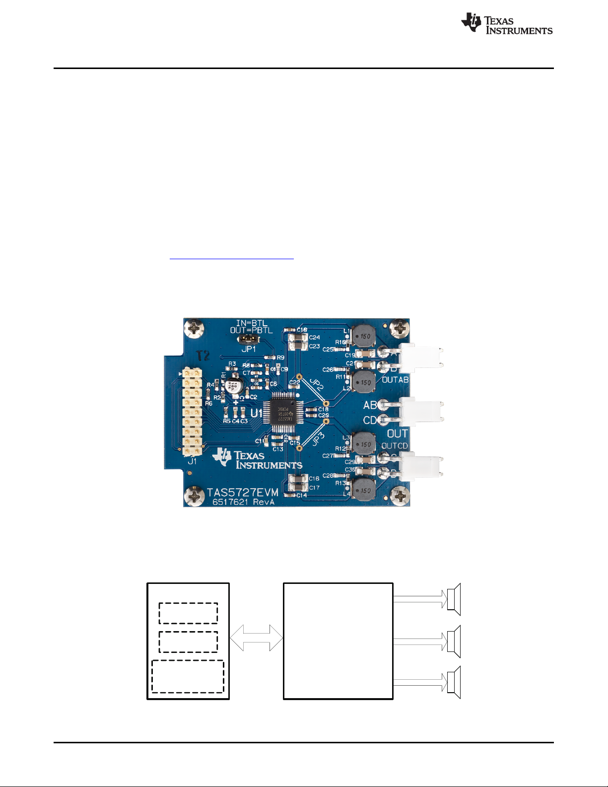
Figure 1. TAS5727EVM Printed-Circuit Board
The EVM together with other TI components on this board, is a complete 2.0-channel digital audio
amplifier system. The MC57XXPSIA Controller board includes a USB interface, a digital input (SPDIF),
analog inputs via the ADC, power inputs, and other features like a mute function and power down.
Figure 2. Complete System and EVM Signal Path Overview
TAS5727 25W Digital Input Amplifier—with EQ and 2-Band DRC SLOU299–December 2010
© 2010, Texas Instruments Incorporated
Submit Documentation Feedback
Page 3
Analog In to ADC
Coaxial SPDIF Input
Optical SPDIF Input
USB Port
5V Supply for
System Power
8V–26V Supply for Output Power
Speaker
Out PBTL
Speaker
Out C & D
Speaker
Out A & B
www.ti.com
1.1 TAS5727EVM and MC57xxPSIA Features
• Channel evaluation module design
• Self-contained protection systems and control pins
• USB interface
• Standard I2S data input using optical or coaxial inputs
• Analog input through analog-to-digital converter
• Subwoofer connection—the PWM terminal provides the PWM signal and power to an external
subwoofer board
• Double-sided, plated-through PCB, 1oz copper, 2mm
• Access to control signal gain and data format through EVM-software GUI
2 Installation
This section describes the EVM and software installation.
2.1 EVM Installation
Installation
The following are the basic tools for the initial EVM power up.
• 5V, 1A power supply (VIN)
• 8–26V, 4A power supply (PVDD)
• Banana-plug test leads for power supplies and speakers
• Optical or coaxial cable for SPDIF interface based on signal source
• USB cable
• EVM software
• Two 8Ω speakers or loads
The following sections describe the TAS5727EVM board in regards to power supply (PSU) and system
interfaces.
SLOU299–December 2010 TAS5727 25W Digital Input Amplifier—with EQ and 2-Band DRC
Submit Documentation Feedback
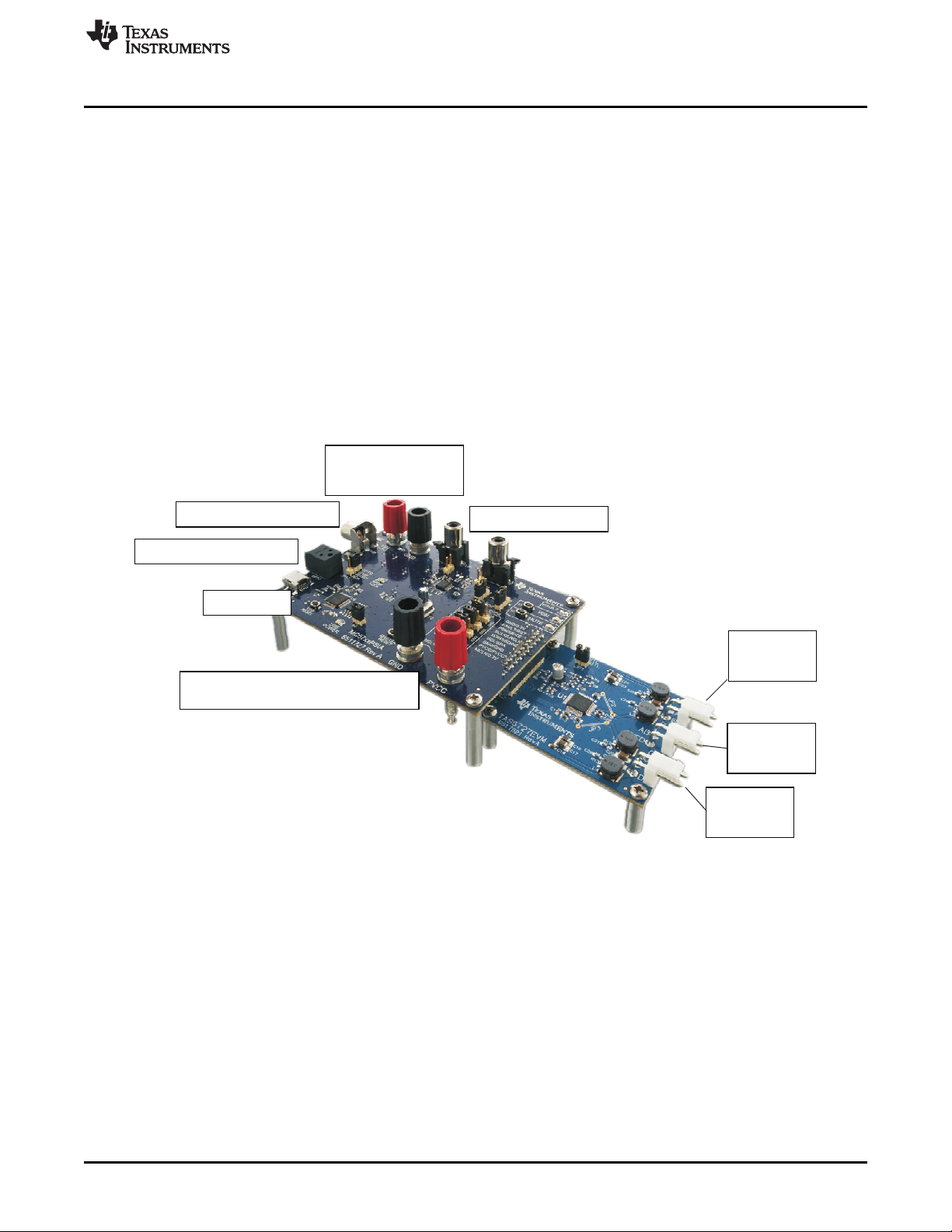
Figure 3. General Connection Picture
© 2010, Texas Instruments Incorporated
3
Page 4
Installation
2.1.1 Connecting the TAS5727EVM to MC57xxPSIA
On the right side of the MC57xxPSIA is a terminal block and another on the left of the TAS5727EVM
(labeled J1). Carefully place the MC57xxPSIA block above the TAS5727EVM block and gently push down.
Figure 4. Connecting TAS5727EVM to MC57xxPSIA
2.1.2 PSU Interface
The TAS5727EVM is powered by two power supplies connected to the MC57xxPSIA controller board: a
5V power supply (VIN), and a 8V-to-26V (PVDD) power supply. The 3.3V level is generated from the 5V
supply by an on-board voltage regulator.
NOTE: The power-supply cable length must be minimized. Increasing the length of the PSU cable
increases the distortion of the amplifier at high output levels and low frequencies.
www.ti.com
The maximum output-stage supply voltage depends on the speaker load resistance. See the
recommended maximum supply voltage in the TAS5727EVM data sheet.
Description Voltage Limitations (8-Ω Load) Current Recommendations
System power supply 5V 1A
Output power stage supply 8–26V 4A
(1)
The rated current corresponds to two channels, full scale.
2.1.3 Loudspeaker Connectors
All speaker outputs are biased at Vcc/2 and must not be connected to ground
(e.g., through an oscilloscope ground).
Loudspeaker connections vary by device setup. When connecting a speaker in BTL mode, connect the
speaker’s two terminals (A and B or C and D) across two outputs on the TAS5727EVM.
Speakers or loads can be connected to the outputs A-D with clip leads, or cables can be made
with female connectors (JST VHR-2N) that can mate to male connectors on the EVM board.
Table 1. Recommended Power Supplies
(1)
CAUTION
4
TAS5727 25W Digital Input Amplifier—with EQ and 2-Band DRC SLOU299–December 2010
© 2010, Texas Instruments Incorporated
Submit Documentation Feedback
Page 5

+
–
OUTB
OUT A
www.ti.com
2.1.4 USB Interface
The TAS5727 registers are accessed through I2C™ bus lines SDA and SCL. The USB circuit and USB
connector on the MC57xxPSIA board facilitates the connection between a host computer and the device.
The EVM USB circuit is powered by the 5V USB line of the host PC and is independent of the power
supplies available on the board. The USB device that is used is a TAS1020B from Texas Instruments.
2.1.5 Digital Audio Interface SPDIF
The Digital Audio Interface SPDIF (RCA/OPTO) accepts digital audio data using the I2S protocol. See the
TAS5727 data sheet for more information.
The RCA connector and the OPTO connector are the two SPDIF interfaces on the MC57xxPSIA board.
The switch S3 toggles between the OPTO and RCA connector to accommodate the signal source. When
the RCA cable or optical cable is connected and the signal source is powered up, verify that the SPDIF
lock indicator (blue LED5) illuminates, confirming that a viable signal is available to the device. Install a
jumper on JP4 across the middle pin and the pin marked SPDIF to connect the digital source to SDIN1.
Install a jumper on JP5 to connect the digital source to SDIN2.
For detailed information on how the data and clocks are provided to the TAS5727, see the schematic
appearing at the end of this document and the DIR9001 device data sheet (SLES198).
Installation
Figure 5. BTL Connection
2.1.6 ADC Interface
In the absence of a digital signal source, the PCM1808 ADC can be used to convert an analog audio
signal to a digital signal to the TAS5727. The DIR9001 still provides clock signals to the ADC in this
process. A 12MHz crystal is installed on the MC57xxPSIA board. The ADC is an additional feature of this
board to provide flexibility in sourcing an audio signal to the TAS5727. Review the PCM1808 data sheet
(SLES177) for a detailed description of the ADC on this EVM. Install the jumper on JP4 across the middle
pin and the pin marked ADC to select ADC as the source for SDIN1.
2.1.7 Board Power-Up General Guidelines
Connect theMC57xxPSIA and the TAS5727EVM boards by locating pin 1 on each board, indicated by a
small white triangle. TheMC57xx plugs down onto the TAS5727EVM board (i.e., the TAS5727EVM board
fits underneath the MC57xxPSIA board). Pin 1 on each board must be connected to each other.
Install the EVM software on the PC before powering up the board. After connecting the loudspeakers or
other loads, power supplies, and the data line, power up the 5V power supply first; then power up the
PVDD power supply. It is recommended initially to set the PVDD level to 10V, then ramp it up to 20V to
verify cable connections.
2.2 Software Installation
Download the TAS57x UI from the TI Web site. The TI Web site always has the latest release and any
updates to versions of the GUI.
SLOU299–December 2010 TAS5727 25W Digital Input Amplifier—with EQ and 2-Band DRC
Submit Documentation Feedback
© 2010, Texas Instruments Incorporated
5
Page 6

Installation
Execute the GUI install program, Setup.exe. Once the program is installed, the program group and
shortcut icon is created in Start → Program → Texas Instruments Inc → TAS57x UI. The GUI launches as
shown in Figure 7.
The TAS5717 tab opens when the GUI starts. Select Devices → TAS57XX → TAS5727 to open the
TAS5727 tab. This tab has two subwindows. One shows the Process Flow window. From the Process
Flow window, each of the signal-processing function tools can be selected by clicking on it. The Biquad
GUI and the DRC GUI can be opened by right-clicking. This window also shows Input select, Mode select,
Channel, and Master Volume. All functions are shown in the same order as in the device.
The other subwindow, the Properties window, has the properties that a user can update by selecting from
the available options. The properties available depend on the device selected.
www.ti.com
6
TAS5727 25W Digital Input Amplifier—with EQ and 2-Band DRC SLOU299–December 2010
© 2010, Texas Instruments Incorporated
Submit Documentation Feedback
Page 7
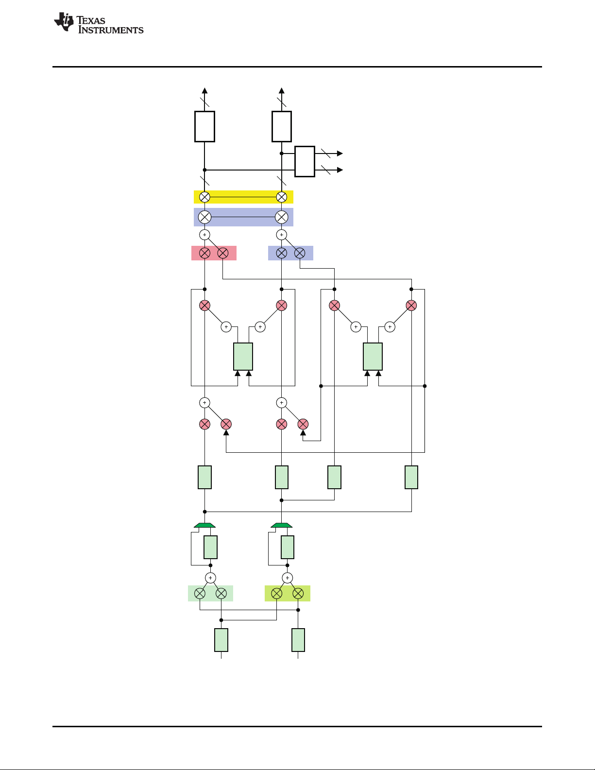
R
L
9BQ
9BQ
B0321-11
0x72
0x76
0x73
0x77
27–2F
I C Subaddress in Red
2
I C:57
VDISTB
2
I C:0x6B (32Bit-Left Level)
Right Level)
2
I C:0x6C (32 Bit-
2
I C:56
VDISTA
2
31–39
2BQ
5A, 5B
2BQ
5E, 5F
Vol2
Vol1
AGL
Vol
Vol Config Reg 0x0E
Vol
AGL
0x71
0x74 v2im1
0x75
0x46[0]
0x46[1]
0x70
2BQ
2BQ
58, 59
0x51[1]
5C, 5D
1BQ
1BQ
26
30
0x51[0]
0x52[1]
0x52[0]
32
24
24
32
Level
Meter
32
32
clip24
clip24
www.ti.com
Installation
SLOU299–December 2010 TAS5727 25W Digital Input Amplifier—with EQ and 2-Band DRC
Submit Documentation Feedback
Figure 6. Process Structure
© 2010, Texas Instruments Incorporated
7
Page 8

Using the EVM Software
3 Using the EVM Software
3.1 Connect the GUI to the EVM
Open the GUI by clicking Start → All Programs → Texas Instruments Inc → TAS57x → TAS57x GUI.
Connect the MC57xxPSIA board (attached to the TAS5717EVM) to your PC with a USB cable. In the
Properties window, select 1-band or 2-band DRC and select Stereo or Woofer. Stereo is selected for BTL
and Woofer is selected for PBTL Mode.
The master volume is muted by default. Select the master volume block. Type the required volume in the
Properties window.
Connect the GUI to the EVM hardware by clicking Target → Connect. This sends the initialization
commands to the device. Un-check Shutdown and Mute. At this time, if connected properly, audio plays
through the device. When the Connect command is issued, if an error appears indicating a USB problem,
check the connections, and press the USB RESET button on the controller board. Then disconnect and
re-connect from the Target menu.
www.ti.com
Figure 7. Main GUI Display
3.2 I2C Memory Tool
This tool can be opened from GDE (Tools → I2C Memory Tool) or independent of GDE from Start →
Program → Texas Instruments Inc → Memory Tool.
Select I2C as shown in Figure 8.
8
TAS5727 25W Digital Input Amplifier—with EQ and 2-Band DRC SLOU299–December 2010
Figure 8. Memory Tool Window
Submit Documentation Feedback
© 2010, Texas Instruments Incorporated
Page 9

www.ti.com
I2C registers can be written or read using this tool. The I2C command file can be sent by selecting the
command file and Execute command.
3.3 Volume Function
The Individual and Master volume can be selected, and the required volume value can be entered in the
Properties window after selecting the function with the mouse (see Figure 9).
3.4 Biquad GUI
Using the left mouse button, select the PEQ block. In the Properties window, change BiQuadSrc to
BIQUAD GUI. Then double-click on the PEQ block as shown in Figure 10. The Biquad GUI window will
pop up (Figure 11).
Using the EVM Software
Figure 9. Volume Control
Figure 10. Selecting Biquad GUI
SLOU299–December 2010 TAS5727 25W Digital Input Amplifier—with EQ and 2-Band DRC
Submit Documentation Feedback
© 2010, Texas Instruments Incorporated
9
Page 10

Using the EVM Software
www.ti.com
A check mark selects the Biquad. If not selected, the Biquad is in ALL PASS Mode.
The frequency response and phase response plots for the current settings can be viewed and adjusted in
the Frequency Response and Phase Response panes of the Biquad GUI as shown in Figure 11. The
individual Biquad gains must be within ±12db.
Clicking the Apply & Draw button sends all three banks of coefficients to the Frequency Response and
Phase response plots (providing auto bank is enabled).
3.5 DRC GUI
The TAS5727 supports 1-band and 2-band DRC. Select one of the DRC modes from the Properties
window. Then set the DRC threshold for each band by double-clicking the UPPERBAND or LOWERBAND
block and adjusting the sliders as shown in Figure 12.
Figure 11. Biquad GUI Window
10
TAS5727 25W Digital Input Amplifier—with EQ and 2-Band DRC SLOU299–December 2010
Submit Documentation Feedback
© 2010, Texas Instruments Incorporated
Page 11

www.ti.com
The crossover frequency for the 2-band DRC by default is 300Hz. This can be modified by entering a new
value in the property window.
The DRC rates for the softening filter, attack, and release can also be adjusted. To set these rates, first
click on the UPPERBAND or LOWERBAND block. Second, set the RateSliders property to On for that
block. Third, double-click on the block to bring up an advanced DRC options window, as shown in
Figure 13.
Using the EVM Software
Figure 12. DRC Options
Figure 13. Advanced DRC Options
PBTL Mode: To run the device in PBTL Mode, the PBTL pin must be driven high. Then in the GUI, select
woofer instead of stereo (stereo is the default value). The source for PBTL is selected as (L+R)/2, but that
be changed by updating input mixer values.
SLOU299–December 2010 TAS5727 25W Digital Input Amplifier—with EQ and 2-Band DRC
Submit Documentation Feedback
© 2010, Texas Instruments Incorporated
11
Page 12

Using the EVM Software
3.5.1 MODULATION SCHEMES Using The FAULT PIN As An Error Indicator:
The A_SEL_FAULTZ pin is the I2C device address select by default. To re-define this pin as an output,
write '1' to bit D1 of reg 0X05. Once re-programmed as output, this pin indicates a fault condition. Output
will go low for Overcurrent (OC) or undervoltage (UVP) error or overtemperature error (OTE) or
overvoltage error
Common Configurations:
1. 2 × BTL BD Mode
2. 2 × BTL AD Mode
Note:
AD: AD Modulation-Outputs are 180° out of phase
BD: BD Modulation
BTL: Bridge-Tied Load
3.5.1.1 2 X BTL BD (BD mode)
1. Set up the hardware.
2. Select the Input MUX from GDE. In the Properties window, select BD Mode.
3. GDE: Target > Connect.
4. Finally uncheck the shutdown box to bring the device out of Shutdown mode, and adjust the Master
Volume as desired.
www.ti.com
3.5.1.2 2 X BTL AD (Default: AD mode)
1. Set up the hardware.
2. Select the Input MUX from GDE. In the Properties window, select AD Mode.
3. GDE: Target > Connect.
4. Finally uncheck the shutdown box to bring the device out of Shutdown mode, and adjust the Master
Volume as desired.
12
TAS5727 25W Digital Input Amplifier—with EQ and 2-Band DRC SLOU299–December 2010
Submit Documentation Feedback
© 2010, Texas Instruments Incorporated
Page 13

www.ti.com
Jumpers and Control Utilities on MC57xxPSIA board
4 Jumpers and Control Utilities on MC57xxPSIA board
4.1 RCA/OPTICAL Jumpers
Select the jumper to reflect the source whether it is RCA or OPTICAL.
4.2 Switches
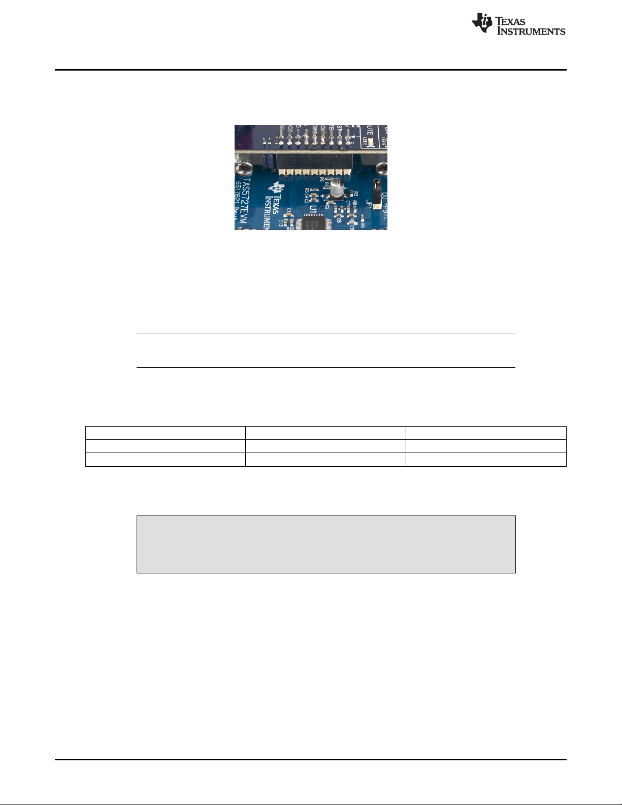
JP1 on the daughter card is for PBTL select. Jumper IN means non-PBTL mode. For PBTL, remove this
jumper.
Reset is an active-low function. Pressing the master reset switch (S2) resets the TAS5727 device; USB
RESET (S1) resets the USB bus. Pressing PDNZ (S4) powers down the TAS5727, and pressing MUTE
(S5) mutes (volume mute) the TAS5727.
4.3 LED Indicators
LED1 : USB Power connector installed at J1
LED2 : 3.3V Power is valid
LED3: RCA connection made
LED4: Optical connection made
LED5: SPDIF signal locked
LED6: FAULT (This LED should be ignored until FAULT is programmed to be an output via I2C write
to reg 0X05.)
LED7: PDN switch (S4) is pressed (closed)
SLOU299–December 2010 TAS5727 25W Digital Input Amplifier—with EQ and 2-Band DRC
Submit Documentation Feedback
© 2010, Texas Instruments Incorporated
13
Page 14

Board Layouts, Bill of Materials, and Schematic
5 Board Layouts, Bill of Materials, and Schematic
5.1 TAS5727EVM and MC57xxPSIA Board Layouts
Figure 14. TAS5727EVM Top Composite Assembly
www.ti.com
14
Figure 15. MC57xxPSIA Top Composite Assembly
TAS5727 25W Digital Input Amplifier—with EQ and 2-Band DRC SLOU299–December 2010
Submit Documentation Feedback
© 2010, Texas Instruments Incorporated
Page 15

www.ti.com
Board Layouts, Bill of Materials, and Schematic
5.2 Bill of Materials
Table 2. Bill of Materials for TAS5727EVM
Manufacturer Part No. Qty Ref Des Vendor Part No. Description Vendor Manufacturer
TI-SEMICONDUCTORS
TAS5727PHP 1 U1 TAS5727PHP 20W DIGAMP WITH DAP HTQFP48-PHP ROHS TEXAS TEXAS
CAPACITORS
GRM1885C1H331JA01D 4 C25, C26, C27, 490-1439-1 CAP SMD0603 CERM 330PFD 50V 5% COG ROHS DIGI-KEY MURATA
GRM188R71H222KA01D 1 C9 490-1500-1 CAP SMD0603 CERM 2200PFD 50V 10% X7R ROHS DIGI-KEY MURATA
GRM188R71H472KA01D 2 C6, C8 490-1506-1 CAP SMD0603 CERM 4700PFD 50V 10% X7R ROHS DIGI-KEY MURATA
GRM188R71H333KA61D 4 C10, C14, C18, 490-3286-1 CAP SMD0603 CERM 0.033UFD 50V 10% X7R ROHS DIGI-KEY MURATA
GRM188R71C473KA01D 2 C5, C7 490-1529-1 CAP SMD0603 CERM 0.047UFD 16V 10% ROHS DIGI-KEY MURATA
C0603C104K8RACTU 4 C2, C4, C11, C12 399-1095-1 CAP SMD0603 CERM 0.1UFD 10V 5% X7R ROHS DIGI-KEY KEMET
GRM188R71H104KA93D 2 C15, C22 490-1519-1 CAP SMD0603 CERM 0.1UFD 50V 10% X7R ROHS DIGI-KEY MURATA
TMK107BJ105KA 1 C13 587-1248-1 CAP SMD0603 CERM 1.0UFD 25V 10% X5R ROHS DIGI-KEY TAIYO YUDEN
C1206C684K5RACTU 4 C19, C21, C29, 445-4013-1 CAP SMD1206 CERM 0.68UFD 50V 10% X7R ROHS DIGI-KEY TDK
C1608X5R0J475M 1 C3 445-1417-1 CAP SMD603 CERM 4.7UFD 6.3V 20% X5R ROHS DIGI-KEY TDK
EEE1CA100SR 1 C1 PCE3878CT CAP SMD ELECT 10ufd 16V 20% VS-B ROHS DIGI-KEY PANASONIC
TMK316B7106KL-TD 4 C16, C17, C23, 587-2399-1 CAP SMD1206 CERM 10UFD 25V 10% X7R ROHS DIGI-KEY TAIYO YUDEN
ERJ-3GEY0R00V 1 R3 P0.0GCT RESISTOR SMD0603 0.0 OHM 5% THICK FILM 1/10W DIGI-KEY PANASONIC
ERJ-3GEYJ180V 4 R10, R11, R12, P18GCT RESISTOR SMD0603 18 OHMS 5% 1/10W ROHS DIGI-KEY PANASONIC
ERJ-3GEYJ471V 2 R7, R8 P470GCT RESISTOR SMD0603 470 OHMS 5% 1/10W ROHS DIGI-KEY PANASONIC
ERJ-3EKF1002V 3 R4, R6, R9 P10.0KHCT RESISTOR SMD0603 10.0K 1% THICK FILM 1/10W ROHS DIGI-KEY PANASONIC
RMCF0603FT15K0 2 R2 RMCF0603FT15K RESISTOR SMD0603 15.0K OHMS 1% 1/10W ROHS DIGI-KEY STACKPOLE
RC0603FR-0718K2L 1 R5 311-18.2KHRCT RESISTOR SMD0603 THICK FILM 18.2K 1% 1/10W ROHS DIGI-KEY YAGEO
DG6045C-150M 4 L1, L2, L3, L4 DG6045C-150M INDUCTOR SMT 15uH X.XA X.X mOHMS 20% DG6045C TOKO JAPAN TOKOJAPAN
PBC02SAAN 1 JP1 S1011E-02 HEADER THRU MALE 2 PIN 100LS GOLD ROHS DIGI-KEY SULLINS
PBC09DAAN 1 J1 S2011E-09 HEADER THRU MALE 2X9 100LS GOLD ROHS DIGI-KEY SULLINS
B2PS-VH(LF)(SN) 3 OUT, OUTAB, 455-1648 JACK JST-VH RA 2-PIN 3.96mmLS ROHS DIGI-KEY JST
SPC02SYAN 1 JP1(2-3) S9001 SHUNT, BLACK AU FLASH 0.100LS DIGI-KEY SULLINS
PMS 440 0025 PH 4 NA H342 4-40 SCREW, STEEL 0.250 IN DIGI-KEY BUILDING
2029 4 NA 2029K STANDOF ,4-40 0.75IN 3/16IN DIA ALUM RND F-F DIGI-KEY KEYSTONE
C2040V-100 2 JP1 C2040V-100 WIRE GRAY STRANDED 20AWG 20mm LENGTH ROHS DIGI-KEY GENERAL
Component Count: 63
C28
C20
C30
C24
RESISTORS
ROHS
R13
0CT ELECTRONICS
INDUCTORS
ROHS
HEADERS AND JACKS
OUTCD
SHUNTS
STANDOFFS, HARDWARE, WIRE
INSTRUMENTS INSTRUMENTS
FASTENERS
ELECTRONICS
CABLE
SLOU299–December 2010 TAS5727 25W Digital Input Amplifier—with EQ and 2-Band DRC
Submit Documentation Feedback
© 2010, Texas Instruments Incorporated
15
Page 16

MCLK
LRCLK
SCLK
SDIN
SCL
SDA
OUTB
OUTC
OUTD
OUTA
0.1ufd/50V
0603
C15
PGND
PVDD
0.033ufd/50V
0603
C18
0.033ufd/50V
0603
C20
PGND
0.1ufd/10V
0603
C12
PGND
PGND
4700pfd/50V
0603
C6
0.1ufd/10V
0603
C2
AVSS
0.0
0603
R3
PGND
4700pfd/50V
0603
C8
0.047ufd/16V
0603
C5
470
0603
R7
0.047ufd/16V
0603
C7
470
0603
R8
18.2K
0603
R5
PGND
PGND
0.1ufd/10V
0603
C4
4.7ufd/6.3V
0603
C3
PGND
1.0in
1.0in
1.0in
1.0in
PGND
PGND
PGND
PGND
1.0ufd/25V
0603
C13
PGND
PGND
J1
18
17
16
15
14
13
12
11
10
9
8
7
6
5
4
3
2
1
PGND
PVDD
AVDD
10.0K
0603
R6
DVDD
AVDD
DVDD
AVDD
PGND
PGND
PGND
PGND
HTQFP48-PHP
U1
PowerPad
0.033ufd/50V
0603
C14
PGND
10.0K
0603
R4
DNP
0603
R1
15.0K
0603
R2
PGND
AVDD
JP1
2
1
10.0K
0603
R9
2200pfd/50V
0603
C9
0.033ufd/50V
0603
C10
0.68ufd/50V
1206
C19
330pfd/50V
0603
C25
18
0603
R10
PGND
330pfd/50V
0603
C26
18
0603
R11
0.68ufd/50V
1206
C21
PGND
PGND
PGND
330pfd/50V
0603
C27
18
0603
R12
HTQFP48-PHP
13
14
15
16
17
18
19
20
21
22
23
24
25 26 282930 3132 333435 36
37
38
39
40
41
42
43
44
45
46
47
48
U1
TAS5727PHP
12345689
1011
12
27
7
0.68ufd/50V
1206
C29
PGND
0.68ufd/50V
1206
C30
PGND
10ufd/25V
1206
C16
PGND
10ufd/25V
1206
C17
PGND
0.1ufd/50V
0603
C22
PGND
PVDD
10ufd/25V
1206
C23
PGND
10ufd/25V
1206
C24
PGND
PGND
330pfd/50V
0603
C28
18
0603
R13
10ufd/16V
VS-B
C1
+
AVDD
0.1ufd/10V
0603
C11
PGND
L1
DG6045C
15uH
15uH
DG6045C
L2
L3
DG6045C
15uH
15uH
DG6045C
L4
JST-VH2-RA
2
1
OUTAB
OUT
1
2
JST-VH2-RA
JST-VH2-RA
2
1
OUTCD
JP3
2
1
10mm
10mm
JP2
2
1
PGND
AVSS
A+B
C+D
PVDD_B/C CAN BE UNROUTED
AT USERS DISCRETION
IN=BTL
OUT=PBTL
STANDOFFS
ANALOG
OUTPUTS
FROM
MC57xxPSIA
BTL
PBTL
BTL
LRCLK
SCLK
SDIN
SDA
SCL
MCLK
IN=PBTL
OUT=BTL
IN=PBTL
OUT=BTL
Board Layouts, Bill of Materials, and Schematic
5.3 Schematics
The schematic for TAS5727EVM follows. The schematics for MC57xxPSIA appear on the following pages.
www.ti.com
16
TAS5727 25W Digital Input Amplifier—with EQ and 2-Band DRC SLOU299–December 2010
© 2010, Texas Instruments Incorporated
Submit Documentation Feedback
Page 17

USB I/O
(A0 IN DEFAULT)
USB BOOT EPROM
DECOUPLING
TO EVM BOARD
USB RESET
TAS1020BPFB
U3
USB INTERFACE
ENGINEERING EVALUATION ONLY
www.ti.com
Board Layouts, Bill of Materials, and Schematic
SLOU299–December 2010 TAS5727 25W Digital Input Amplifier—with EQ and 2-Band DRC
Submit Documentation Feedback
© 2010, Texas Instruments Incorporated
17
Page 18

H
H
1-2:
2-3:
TO ADC
(HIGH)
(LOW)
FMT1
TO
(DEFAULT)
MASTER RESET
INPUT
SELECT
OPTO INPUT
RCA INPUT
SPDIF INPUT
OPTO INPUT
RCA INPUT
TO SPDIF
SPDIF DECOUPLING
24Bit/MSB/I2S
FMT0
DATA FORMAT
EVM BOARD
ADC
TO
LOCK
SPDIF
SPDIF
3.3V@1A
TO ADC
U5
DIR9001PW
5V POWER INPUT
TO EVM BOARD
JP1 IN: SCKO = 512 Fs
JP1 OUT: SCKO = 256 Fs
SPDIF RECEIVER
ENGINEERING EVALUATION ONLY
Board Layouts, Bill of Materials, and Schematic
www.ti.com
18
TAS5727 25W Digital Input Amplifier—with EQ and 2-Band DRC SLOU299–December 2010
© 2010, Texas Instruments Incorporated
Submit Documentation Feedback
Page 19

(SDIN2)
(SDIN1)
PDN
MC012
PSIA
MUTE
(1-2)
(2-3)
HIGH POWER INPUT
FROM USB
FROM
SPDIF
5V DECOUPLING
TO EVM BOARDS
FROM
FAULT
FROM VR1
MASETER RESET
ANALOG INPUTS
3.3V DECOUPLING
NOTES ON JUMPERS
IN: LIN/RIN = 1Vrms MAX.
OUT: LIN/RIN = 2Vrms MAX.
PCM1808PW
ADC
ENGINEERING EVALUATION ONLY
ADC / CONNECTOR I/O
www.ti.com
Board Layouts, Bill of Materials, and Schematic
SLOU299–December 2010 TAS5727 25W Digital Input Amplifier—with EQ and 2-Band DRC
Submit Documentation Feedback
© 2010, Texas Instruments Incorporated
19
Page 20

EVALUATION BOARD/KIT IMPORTANT NOTICE
Texas Instruments (TI) provides the enclosed product(s) under the following conditions:
This evaluation board/kit is intended for use for ENGINEERING DEVELOPMENT, DEMONSTRATION, OR EVALUATION PURPOSES
ONLY and is not considered by TI to be a finished end-product fit for general consumer use. Persons handling the product(s) must have
electronics training and observe good engineering practice standards. As such, the goods being provided are not intended to be complete
in terms of required design-, marketing-, and/or manufacturing-related protective considerations, including product safety and environmental
measures typically found in end products that incorporate such semiconductor components or circuit boards. This evaluation board/kit does
not fall within the scope of the European Union directives regarding electromagnetic compatibility, restricted substances (RoHS), recycling
(WEEE), FCC, CE or UL, and therefore may not meet the technical requirements of these directives or other related directives.
Should this evaluation board/kit not meet the specifications indicated in the User’s Guide, the board/kit may be returned within 30 days from
the date of delivery for a full refund. THE FOREGOING WARRANTY IS THE EXCLUSIVE WARRANTY MADE BY SELLER TO BUYER
AND IS IN LIEU OF ALL OTHER WARRANTIES, EXPRESSED, IMPLIED, OR STATUTORY, INCLUDING ANY WARRANTY OF
MERCHANTABILITY OR FITNESS FOR ANY PARTICULAR PURPOSE.
The user assumes all responsibility and liability for proper and safe handling of the goods. Further, the user indemnifies TI from all claims
arising from the handling or use of the goods. Due to the open construction of the product, it is the user’s responsibility to take any and all
appropriate precautions with regard to electrostatic discharge.
EXCEPT TO THE EXTENT OF THE INDEMNITY SET FORTH ABOVE, NEITHER PARTY SHALL BE LIABLE TO THE OTHER FOR ANY
INDIRECT, SPECIAL, INCIDENTAL, OR CONSEQUENTIAL DAMAGES.
TI currently deals with a variety of customers for products, and therefore our arrangement with the user is not exclusive.
TI assumes no liability for applications assistance, customer product design, software performance, or infringement of patents or
services described herein.
Please read the User’s Guide and, specifically, the Warnings and Restrictions notice in the User’s Guide prior to handling the product. This
notice contains important safety information about temperatures and voltages. For additional information on TI’s environmental and/or
safety programs, please contact the TI application engineer or visit www.ti.com/esh.
No license is granted under any patent right or other intellectual property right of TI covering or relating to any machine, process, or
combination in which such TI products or services might be or are used.
FCC Warning
This evaluation board/kit is intended for use for ENGINEERING DEVELOPMENT, DEMONSTRATION, OR EVALUATION PURPOSES
ONLY and is not considered by TI to be a finished end-product fit for general consumer use. It generates, uses, and can radiate radio
frequency energy and has not been tested for compliance with the limits of computing devices pursuant to part 15 of FCC rules, which are
designed to provide reasonable protection against radio frequency interference. Operation of this equipment in other environments may
cause interference with radio communications, in which case the user at his own expense will be required to take whatever measures may
be required to correct this interference.
EVM WARNINGS AND RESTRICTIONS
It is important to operate this EVM within the input voltage range of -0.5V to 4.1V and the output voltage range of 26Vp-p.
Exceeding the specified input range may cause unexpected operation and/or irreversible damage to the EVM. If there are questions
concerning the input range, please contact a TI field representative prior to connecting the input power.
Applying loads outside of the specified output range may result in unintended operation and/or possible permanent damage to the EVM.
Please consult the EVM User's Guide prior to connecting any load to the EVM output. If there is uncertainty as to the load specification,
please contact a TI field representative.
During normal operation, some circuit components may have case temperatures greater than 85°C. The EVM is designed to operate
properly with certain components above 85°C as long as the input and output ranges are maintained. These components include but are
not limited to linear regulators, switching transistors, pass transistors, and current sense resistors. These types of devices can be identified
using the EVM schematic located in the EVM User's Guide. When placing measurement probes near these devices during operation,
please be aware that these devices may be very warm to the touch.
Mailing Address: Texas Instruments, Post Office Box 655303, Dallas, Texas 75265
Copyright © 2008-2009, Texas Instruments Incorporated
Page 21

IMPORTANT NOTICE
Texas Instruments Incorporated and its subsidiaries (TI) reserve the right to make corrections, modifications, enhancements, improvements,
and other changes to its products and services at any time and to discontinue any product or service without notice. Customers should
obtain the latest relevant information before placing orders and should verify that such information is current and complete. All products are
sold subject to TI’s terms and conditions of sale supplied at the time of order acknowledgment.
TI warrants performance of its hardware products to the specifications applicable at the time of sale in accordance with TI’s standard
warranty. Testing and other quality control techniques are used to the extent TI deems necessary to support this warranty. Except where
mandated by government requirements, testing of all parameters of each product is not necessarily performed.
TI assumes no liability for applications assistance or customer product design. Customers are responsible for their products and
applications using TI components. To minimize the risks associated with customer products and applications, customers should provide
adequate design and operating safeguards.
TI does not warrant or represent that any license, either express or implied, is granted under any TI patent right, copyright, mask work right,
or other TI intellectual property right relating to any combination, machine, or process in which TI products or services are used. Information
published by TI regarding third-party products or services does not constitute a license from TI to use such products or services or a
warranty or endorsement thereof. Use of such information may require a license from a third party under the patents or other intellectual
property of the third party, or a license from TI under the patents or other intellectual property of TI.
Reproduction of TI information in TI data books or data sheets is permissible only if reproduction is without alteration and is accompanied
by all associated warranties, conditions, limitations, and notices. Reproduction of this information with alteration is an unfair and deceptive
business practice. TI is not responsible or liable for such altered documentation. Information of third parties may be subject to additional
restrictions.
Resale of TI products or services with statements different from or beyond the parameters stated by TI for that product or service voids all
express and any implied warranties for the associated TI product or service and is an unfair and deceptive business practice. TI is not
responsible or liable for any such statements.
TI products are not authorized for use in safety-critical applications (such as life support) where a failure of the TI product would reasonably
be expected to cause severe personal injury or death, unless officers of the parties have executed an agreement specifically governing
such use. Buyers represent that they have all necessary expertise in the safety and regulatory ramifications of their applications, and
acknowledge and agree that they are solely responsible for all legal, regulatory and safety-related requirements concerning their products
and any use of TI products in such safety-critical applications, notwithstanding any applications-related information or support that may be
provided by TI. Further, Buyers must fully indemnify TI and its representatives against any damages arising out of the use of TI products in
such safety-critical applications.
TI products are neither designed nor intended for use in military/aerospace applications or environments unless the TI products are
specifically designated by TI as military-grade or "enhanced plastic." Only products designated by TI as military-grade meet military
specifications. Buyers acknowledge and agree that any such use of TI products which TI has not designated as military-grade is solely at
the Buyer's risk, and that they are solely responsible for compliance with all legal and regulatory requirements in connection with such use.
TI products are neither designed nor intended for use in automotive applications or environments unless the specific TI products are
designated by TI as compliant with ISO/TS 16949 requirements. Buyers acknowledge and agree that, if they use any non-designated
products in automotive applications, TI will not be responsible for any failure to meet such requirements.
Following are URLs where you can obtain information on other Texas Instruments products and application solutions:
Products Applications
Amplifiers amplifier.ti.com Audio www.ti.com/audio
Data Converters dataconverter.ti.com Automotive www.ti.com/automotive
DLP® Products www.dlp.com Communications and www.ti.com/communications
DSP dsp.ti.com Computers and www.ti.com/computers
Clocks and Timers www.ti.com/clocks Consumer Electronics www.ti.com/consumer-apps
Interface interface.ti.com Energy www.ti.com/energy
Logic logic.ti.com Industrial www.ti.com/industrial
Power Mgmt power.ti.com Medical www.ti.com/medical
Microcontrollers microcontroller.ti.com Security www.ti.com/security
RFID www.ti-rfid.com Space, Avionics & www.ti.com/space-avionics-defense
RF/IF and ZigBee® Solutions www.ti.com/lprf Video and Imaging www.ti.com/video
Mailing Address: Texas Instruments, Post Office Box 655303, Dallas, Texas 75265
Copyright © 2010, Texas Instruments Incorporated
Telecom
Peripherals
Defense
Wireless www.ti.com/wireless-apps
 Loading...