

Page 1

TAS5711
www.ti.com
SLOS600 –DECEMBER 2009
20-W DIGITAL AUDIO-POWER AMPLIFIER WITH EQ, DRC, AND 2.1 MODE
Check for Samples: TAS5711
1
FEATURES
2
• Audio Input/Output
– 20-W Into an 8-Ω Load From an 18-V Supply – Up to 90% Efficient
– Wide PVDD Range, From 8 V to 26 V – AD and BD Filter Mode Support
– Efficient Class-D Operation Eliminates – SNR: 106 dB, A-Weighted
Need for Heatsinks
– One Serial Audio Input (Two Audio Performance
Channels)
– 2.1 Mode (2 SE + 1 BTL) Be Used As Power Limiter. Enables
– 2.0 Mode (2 BTL)
– Single-Filter PBTL Mode Support
– I2C Address Selection Pin (Chip Select)
– Supports 8-kHz to 48-kHz Sample Rate
(LJ/RJ/I2S)
• Audio/PWM Processing
– Independent Channel Volume Controls With
24-dB to Mute
– Separate Dynamic Range Control for
Satellite and Subchannels
– 21 Programmable Biquads for Speaker EQ
and Other Audio Processing Features
– Programmable Coefficients for DRC Filters APPLICATIONS – DC Blocking Filters – Support for 3D Effects
• General Features
– Serial Control Interface Operational Without
MCLK
– Factory-Trimmed Internal Oscillator for
Automatic Rate Detection
– Surface Mount, 48-Pin, 7-mm × 7-mm
HTQFP Package
– Thermal and Short-Circuit Protection
– Support for AD or BD Mode
• Benefits
– EQ: Speaker Equalization Improves Audio
– DRC: Dynamic Range Compression. Can
Speaker Protection, Easy Listening,
Night-Mode Listening.
– Separate DRC for Satellite and
Subchannels
– Autobank Switching: Preload Coefficients
for Different Sample Rates. No Need to
Write new Coefficients to the Part When
Sample Rate Changes.
– Autodetect: Automatically Detects
Sample-Rate Changes. No Need for
External Microprocessor Intervention
• Requires Only 3.3 V and PVDD
• Television
• iPod™ Dock
• Sound Bar
DESCRIPTION
The TAS5711 is a 20-W, efficient, digital audio power
amplifier for driving stereo bridge-tied speakers. One
serial data input allows processing of up to two
discrete audio channels and seamless integration to
most digital audio processors and MPEG decoders.
The device accepts a wide range of input data and
data rates. A fully programmable data path routes
these channels to the internal speaker drivers.
The TAS5711 is an I2S slave-only device receiving all
clocks from external sources. The TAS5711 operates
with a PWM carrier between 384-kHz switching rate
and 352-KHz switching rate depending on the input
sample rate. Oversampling combined with a
fourth-order noise shaper provides a flat noise floor
and excellent dynamic range from 20 Hz to 20 kHz.
1
Please be aware that an important notice concerning availability, standard warranty, and use in critical applications of Texas
Instruments semiconductor products and disclaimers thereto appears at the end of this data sheet.
2iPod is a trademark of Apple Inc.
PRODUCTION DATA information is current as of publication date.
Products conform to specifications per the terms of the Texas
Instruments standard warranty. Production processing does not
necessarily include testing of all parameters.
Copyright © 2009, Texas Instruments Incorporated
Page 2
SDIN
LRCLK
SCLK
MCLK
RESET
PDN
SDA
PLL_FLTM
PLL_FLTP
AVDD/DVDD
PVDD
OUT_A
OUT_C
OUT_B
OUT_D
BST_A
BST_C
BST_B
BST_D
3.3 V 8 V–26 V
SCL
Digital
Audio
Source
I C
Control
2
Control
Inputs
LC
SE
LC
BTL
B0264-09
Loop
Filter
(1)
LC
SE
PVDD
PVDD
A_SEL( )FAULT
TAS5711
SLOS600 –DECEMBER 2009
This integrated circuit can be damaged by ESD. Texas Instruments recommends that all integrated circuits be handled with
appropriate precautions. Failure to observe proper handling and installation procedures can cause damage.
ESD damage can range from subtle performance degradation to complete device failure. Precision integrated circuits may be more
susceptible to damage because very small parametric changes could cause the device not to meet its published specifications.
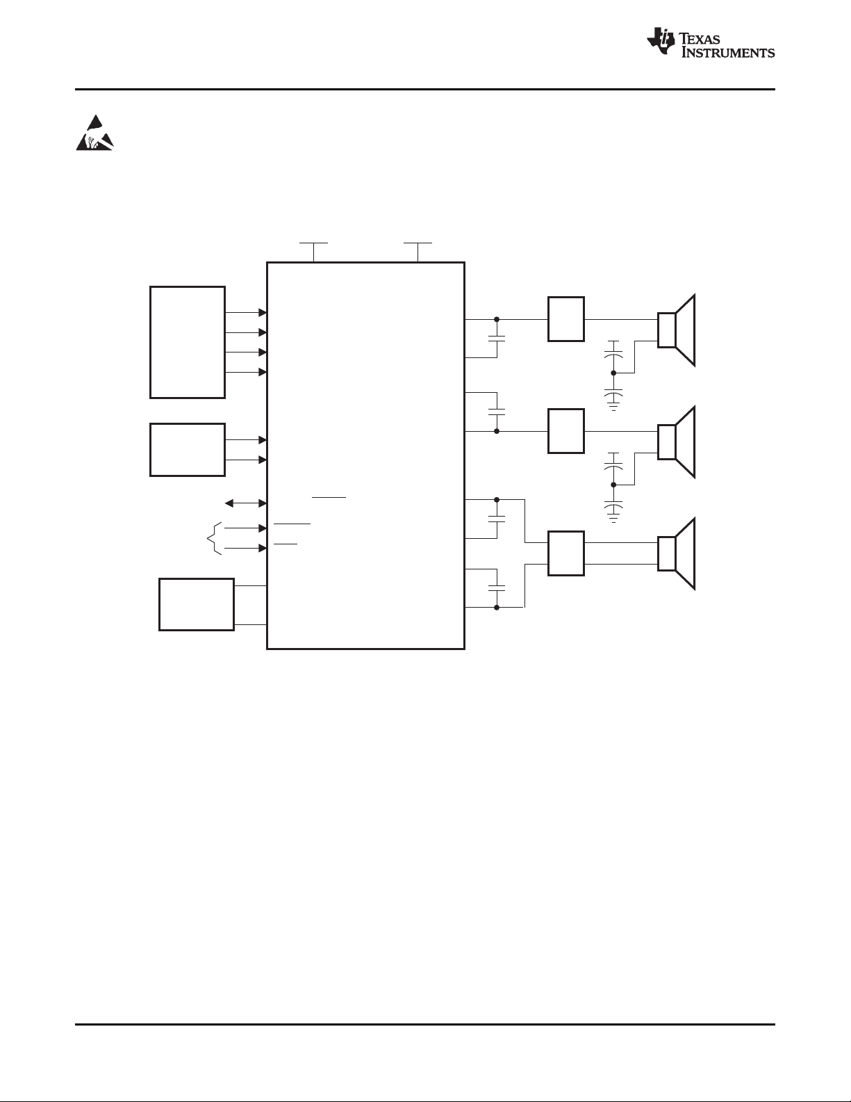
SIMPLIFIED APPLICATION DIAGRAM
www.ti.com
(1) See TAS5711 EVM User's Guide (SLOU280) for loop filter values.
2 Submit Documentation Feedback Copyright © 2009, Texas Instruments Incorporated
Product Folder Link(s): TAS5711
Page 3

SDIN
MCLK
SCLK
LRCLK
Serial
Audio
Port
Protection
Logic
ClickandPop
Control
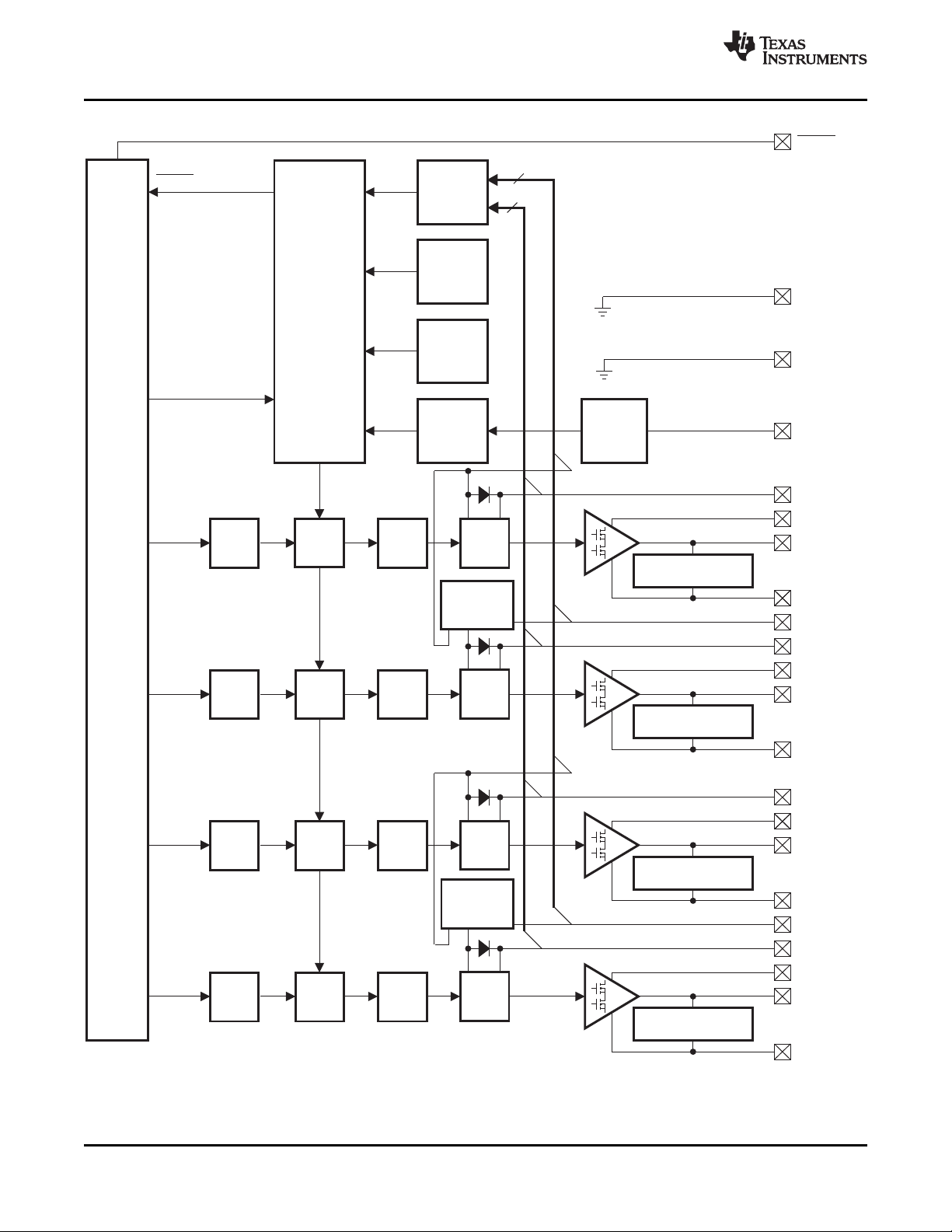
Digital AudioProcessor
(DAP)
SDA
SCL
4
Order
th
Noise
Shaper
and
PWM
S
R
C
SampleRate
Autodetect
andPLL
Serial
Control
Microcontroller
Based
System
Control
TerminalControl
OUT_A
OUT_B
2 HB´
FET Out
OUT_C
OUT_D
2 HB´
FET Out
B0262-06
TAS5711
www.ti.com
FUNCTIONAL VIEW
SLOS600 –DECEMBER 2009
Copyright © 2009, Texas Instruments Incorporated Submit Documentation Feedback 3
Product Folder Link(s): TAS5711
Page 4
Temp.
Sense
VALID
FAULT
AGND
OC_ADJ
Power
On
Reset
Under-
voltage
Protection
GND
PWM_D
OUT_D
PGND_CD
PVDD_D
BST_D
Gate
Drive
PWM
Rcv
Overcurrent
Protection
4
Protection
and
I/OLogic
PWM_C
OUT_C
PGND_CD
PVDD_C
BST_C
Timing
Gate
Drive
Ctrl
PWM
Rcv
GVDD_CD
PWM_B
OUT_B
PGND_AB
PVDD_B
BST_B
Timing
Gate
Drive
Ctrl
PWM
Rcv
PWM_A
OUT_A
PGND_AB
PVDD_A
BST_A
Timing
Gate
Drive
Ctrl
PWM
Rcv
GVDD_AB
Ctrl
PulldownResistor
PulldownResistor
PulldownResistor
PulldownResistor
4
GVDD_CD
Regulator
GVDD_AB
Regulator
Timing
I
sense
B0034-05
PWMController
FAULT
TAS5711
SLOS600 –DECEMBER 2009
www.ti.com
Figure 1. Power Stage Functional Block Diagram
4 Submit Documentation Feedback Copyright © 2009, Texas Instruments Incorporated
Product Folder Link(s): TAS5711
Page 5
+
L
R
+
+
+
+
+
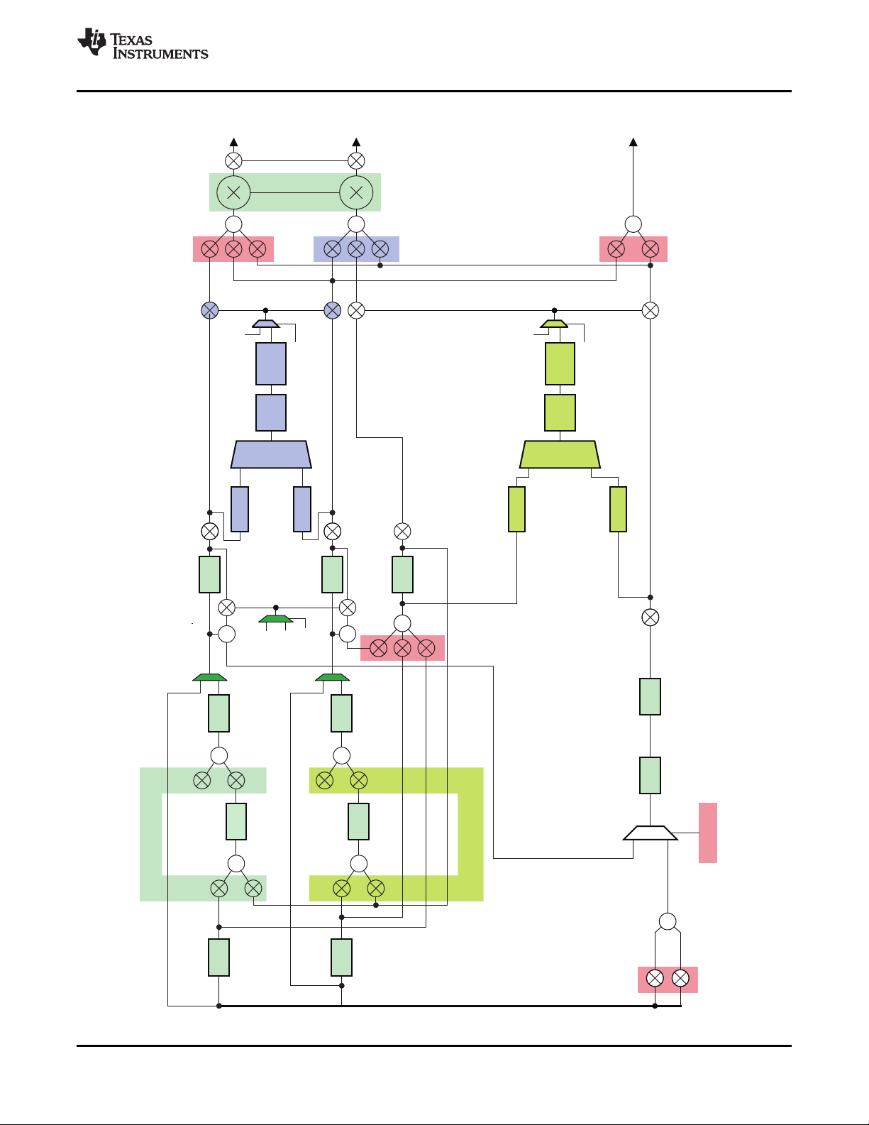
Vol1
Vol2
ealpha
1BQ
1BQ
1BQ
1BQ
6BQ
6BQ
1BQ
1BQ
1BQ
Input Muxing
Log
Math
Attack
Decay
1
Master ON/OFF
(0x46[0])
Energy
MAXMUX
ealpha
B0321-08
1
1
1
1
1
1
51 V1OM
52 V2OM
I2C:57
VDISTB
I2C:56
VDISTA
60 V6OM
55
2A
I2C:53 – V1IM
31
2B–2F, 58
32–36, 5C
59
I C Subaddress in Red
2
5D
5E
29
30
I2C:54 – V2IM
L
R
1BQ
1BQ
Vol1
5A
5B
21 (D8, D9)
½
½
61
+
+
+
–1
0
Auto-lp
(0x46 Bit 5)
Log
Math
Attack
Decay
1
Master ON/OFF
(0x46[1])
Energy
MAXMUX
ealpha
ealpha
ealpha
Vol2
+
+
3D
3D
3A
3A
TAS5711
www.ti.com
DAP Process Structure
SLOS600 –DECEMBER 2009
Copyright © 2009, Texas Instruments Incorporated Submit Documentation Feedback 5
Product Folder Link(s): TAS5711
Page 6
SSTIMER
OC_ADJ
PLL_FLTP
VR_ANA
PBTL
AVSS
PLL_FLTM
BST_A
GVDD_OUT
PVDD_A
OUT_A
RESET
PVDD_A
STEST
PDN
VR_DIG
OSC_RES
DVSSO
DVDD
MCLK
A_SEL
SCLK
SDIN
LRCLK
AVDD
SDA
SCL
DVSS
GND
VREG
BST_B
PVDD_B
PVDD_C
OUT_C
PVDD_D
BST_D
PGND_AB
OUT_B
PGND_CD
OUT_D
AGND
PGND_AB
PVDD_B
PGND_CD
PVDD_D
BST_C
PVDD_C
GVDD_OUT
P0075-08
PHP Package
(TopView)
TAS5711
1
2
3
4
5
6
7
8
9
10
11
12
13
14
15 161718 19 20
21 222324
25
26
27
28
29
30
31
32
484746
45 44
43 42 41 40 39 38 37
36
35
34
33
TAS5711
SLOS600 –DECEMBER 2009
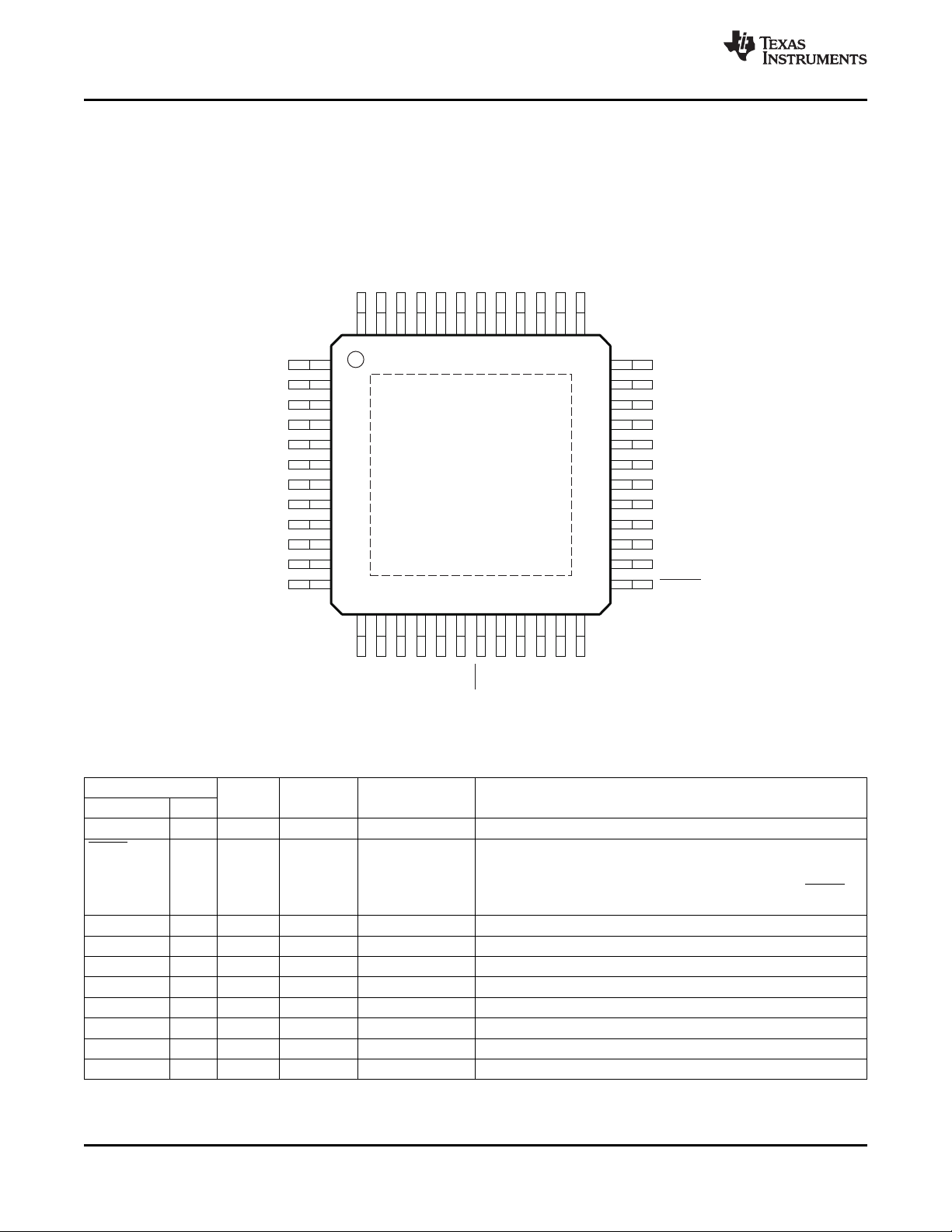
PIN ASSIGNMENT
www.ti.com
DEVICE INFORMATION
PIN
NAME NO.
AGND 30 P Analog ground for power stage
A_SEL 14 DIO A value of 0 (15-kΩ pulldown) makes the I2C device address 0x34,
AVDD 13 P 3.3-V analog power supply
AVSS 9 P Analog 3.3-V supply ground
BST_A 4 P High-side bootstrap supply for half-bridge A
BST_B 43 P High-side bootstrap supply for half-bridge B
BST_C 42 P High-side bootstrap supply for half-bridge C
BST_D 33 P High-side bootstrap supply for half-bridge D
DVDD 27 P 3.3-V digital power supply
DVSSO 17 P Oscillator ground
(1) TYPE: A = analog; D = 3.3-V digital; P = power/ground/decoupling; I = input; O = output
(2) All pullups are weak pullups and all pulldowns are weak pulldowns. The pullups and pulldowns are included to assure proper input logic
levels if the pins are left unconnected (pullups → logic 1 input; pulldowns → logic 0 input).
(1)
TYPE
5-V
TOLERANT
TERMINATION
PIN FUNCTIONS
(2)
and a value of 1 (15-kΩ pullup) makes it 0x36. This pin can be
programmed after RESET to be an output by writing 1 to bit 0 of I2C
register 0x05. In that mode, the A_SEL pin is redefined as FAULT
(see ERROR REPORTING for details).
DESCRIPTION
6 Submit Documentation Feedback Copyright © 2009, Texas Instruments Incorporated
Product Folder Link(s): TAS5711
Page 7

TAS5711
www.ti.com
SLOS600 –DECEMBER 2009
PIN FUNCTIONS (continued)
PIN
NAME NO.
DVSS 28 P Digital ground
GND 29 P Analog ground for power stage
GVDD_OUT 5, 32 P Gate drive internal regulator output. This pin must not be used to
LRCLK 20 DI 5-V Pulldown Input serial audio data left/right clock (sample rate clock)
MCLK 15 DI 5-V Pulldown Master clock input
OC_ADJ 7 AO Analog overcurrent programming. Requires resistor to ground.
OSC_RES 16 AO Oscillator trim resistor. Connect an 18.2-kΩ 1% resistor to DVSSO.
OUT_A 1 O Output, half-bridge A
OUT_B 46 O Output, half-bridge B
OUT_C 39 O Output, half-bridge C
OUT_D 36 O Output, half-bridge D
PBTL 8 DI Low means BTL or SE mode; high means PBTL mode. Information
PDN 19 DI 5-V Pullup Power down, active-low. PDN prepares the device for loss of power
PGND_AB 47, 48 P Power ground for half-bridges A and B
PGND_CD 37, 38 P Power ground for half-bridges C and D
PLL_FLTM 10 AO PLL negative loop filter terminal
PLL_FLTP 11 AO PLL positive loop filter terminal
PVDD_A 2, 3 P Power supply input for half-bridge output A
PVDD_B 44, 45 P Power supply input for half-bridge output B
PVDD_C 40, 41 P Power supply input for half-bridge output C
PVDD_D 34, 35 P Power supply input for half-bridge output D
RESET 25 DI 5-V Pullup Reset, active-low. A system reset is generated by applying a logic
SCL 24 DI 5-V I2C serial control clock input
SCLK 21 DI 5-V Pulldown Serial audio data clock (shift clock). SCLK is the serial audio port
SDA 23 DIO 5-V I2C serial control data interface input/output
SDIN 22 DI 5-V Pulldown Serial audio data input. SDIN supports three discrete (stereo) data
SSTIMER 6 AI Controls ramp time of OUT_x to minimize pop. Leave this pin
STEST 26 DI Factory test pin. Connect directly to DVSS.
VR_ANA 12 P Internally regulated 1.8-V analog supply voltage. This pin must not
VR_DIG 18 P Internally regulated 1.8-V digital supply voltage. This pin must not be
VREG 31 P Digital regulator output. Not to be used for powering external
TYPE
(1)
5-V
TOLERANT
TERMINATION
(2)
drive external devices.
goes directly to power stage.
supplies by shutting down the Noise Shaper and initiating PWM stop
sequence.
low to this pin. RESET is an asynchronous control signal that
restores the DAP to its default conditions, and places the PWM in
the hard mute state (tristated).
input data bit clock.
formats.
floating for BD mode. Requires capacitor of 2.2 nF to GND in AD
mode. The capacitor determines the ramp time.
be used to power external devices.
used to power external devices.
circuitry.
DESCRIPTION
Copyright © 2009, Texas Instruments Incorporated Submit Documentation Feedback 7
Product Folder Link(s): TAS5711
Page 8
TAS5711
SLOS600 –DECEMBER 2009
www.ti.com
ABSOLUTE MAXIMUM RATINGS
over operating free-air temperature range (unless otherwise noted)
Supply voltage
Input voltage
OUT_x to PGND_x 32
BST_x to PGND_x 43
Input clamp current, I
Output clamp current, I
Operating free-air temperature 0 to 85 °C
Operating junction temperature range 0 to 150 °C
Storage temperature range, T
(1) Stresses beyond those listed under absolute ratings may cause permanent damage to the device. These are stress ratings only and
functional operation of the device at these or any other conditions beyond those indicated under recommended operation conditions are
not implied. Exposure to absolute-maximum conditions for extended periods may affect device reliability.
(2) 5-V tolerant inputs are PDN, RESET, SCLK, LRCLK, MCLK, SDIN, SDA, and SCL.
(3) Maximum pin voltage should not exceed 6.0V
(4) DC voltage + peak ac waveform measured at the pin should be below the allowed limit for all conditions.
DVDD, AVDD –0.3 to 3.6 V
PVDD_x –0.3 to 30 V
OC_ADJ –0.3 to 4.2 V
3.3-V digital input –0.5 to DVDD + 0.5 V
5-V tolerant
(2)
digital input (except MCLK) –0.5 to DVDD + 2.5
5-V tolerant MCLK input –0.5 to AVDD + 2.5
IK
OK
stg
(1)
VALUE UNIT
(3)
(3)
(4)
(4)
V
V
V
V
±20 mA
±20 mA
–40 to 125 °C
DISSIPATION RATINGS
PACKAGE
(1)
DERATING FACTOR TA≤ 25°C TA= 45°C TA= 70°C
ABOVE TA= 25°C POWER RATING POWER RATING POWER RATING
7-mm × 7-mm HTQFP 40 mW/°C 5 W 4.2 W 3.2 W
(1) This data was taken using 1 oz trace and copper pad that is soldered directly to a JEDEC standard high-k PCB. The thermal pad must
be soldered to a thermal land on the printed-circuit board. See TI Technical Briefs SLMA002 for more information about using the
HTQFP thermal pad
RECOMMENDED OPERATING CONDITIONS
MIN NOM MAX UNIT
Digital/analog supply voltage DVDD, AVDD 3 3.3 3.6 V
Half-bridge supply voltage PVDD_x 8 26 V
V
IH
V
IL
T
A
(1)
T
J
High-level input voltage 5-V tolerant 2 V
Low-level input voltage 5-V tolerant 0.8 V
Operating ambient temperature range 0 85 °C
Operating junction temperature range 0 125 °C
RL(BTL) Load impedance Output filter: L = 15 μH, C = 680 nF. 6 8 Ω
LO(BTL) Output-filter inductance μH
Minimum output inductance under 10
short-circuit condition
(1) Continuous operation above the recommended junction temperature may result in reduced reliability and/or lifetime of the device.
PWM OPERATION AT RECOMMENDED OPERATING CONDITIONS
PARAMETER TEST CONDITIONS VALUE UNIT
Output sample rate
11.025/22.05/44.1-kHz data rate ±2% 352.8 kHz
48/24/12/8/16/32-kHz data rate ±2% 384
8 Submit Documentation Feedback Copyright © 2009, Texas Instruments Incorporated
Product Folder Link(s): TAS5711
Page 9
TAS5711
www.ti.com
SLOS600 –DECEMBER 2009
PLL INPUT PARAMETERS AND EXTERNAL FILTER COMPONENTS
PARAMETER TEST CONDITIONS MIN TYP MAX UNIT
f
MCLKI
MCLK Frequency 2.8224 24.576 MHz
MCLK duty cycle 40% 50% 60%
tr /
tf
(MCLK)
Rise/fall time for MCLK 5 ns
LRCLK allowable drift before LRCLK reset 4 MCLKs
External PLL filter capacitor C1 SMD 0603 X7R 47 nF
External PLL filter capacitor C2 SMD 0603 X7R 4.7 nF
External PLL filter resistor R SMD 0603, metal film 470 Ω
ELECTRICAL CHARACTERISTICS
DC Characteristics
TA = 25°, PVCC_x = 18V, DVDD = AVDD = 3.3V, RL= 8Ω, BTL AD Mode, FS = 48KHz (unless otherwise noted)
PARAMETER TEST CONDITIONS MIN TYP MAX UNIT
V
OH
V
OL
I
IL
I
IH
I
DD
I
PVDD
r
DS(on)
I/O Protection
V
uvp
V
uvp,hyst
(3)
OTE
OTE
HYST
OLPC Overload protection counter f
I
OC
I
OCT
R
OCP
R
PD
(1) IIHfor the PBTL pin has a maximum limit of 200 µA due to an intenal pulldown on the pin.
(2) This does not include bond-wire or pin resistance.
(3) Specified by design
High-level output voltage A_SEL and SDA IOH= –4 mA 2.4 V
DVDD = AVDD = 3 V
Low-level output voltage A_SEL and SDA IOL= 4 mA 0.5 V
DVDD = AVDD = 3 V
Low-level input current μA
High-level input current μA
3.3 V supply current mA
3.3 V supply voltage (DVDD,
AVDD)
VI< VIL; DVDD = AVDD 75
= 3.6V
VI> VIH; DVDD = 75
AVDD = 3.6V
Normal Mode 48 70
Reset (RESET = low, 24 32
PDN = high)
Normal Mode 30 55
Half-bridge supply current No load (PVDD_x) mA
Reset (RESET = low, 5 13
PDN = high)
Drain-to-source resistance, LS TJ= 25°C, includes metallization resistance 180
(2)
Drain-to-source resistance,
HS
TJ= 25°C, includes metallization resistance 180
Undervoltage protection limit PVDD falling 7.2 V
Undervoltage protection limit PVDD rising 7.6 V
Overtemperature error 150 °C
Extra temperature drop
(3)
required to recover from error
= 384 kHz 0.63 ms
PWM
Overcurrent limit protection Resistor—programmable, max. current, R
= 22 kΩ 4.5 A
OCP
30 °C
Overcurrent response time 150 ns
OC programming resistor Resistor tolerance = 5% for typical value; the minimum
range resistance should not be less than 20 kΩ.
Internal pulldown resistor at Connected when drivers are tristated to provide bootstrap
the output of each half-bridge capacitor charge.
20 22 kΩ
3 kΩ
(1)
mΩ
Copyright © 2009, Texas Instruments Incorporated Submit Documentation Feedback 9
Product Folder Link(s): TAS5711
Page 10
TAS5711
SLOS600 –DECEMBER 2009
AC Characteristics (BTL)
PVDD_x = 18 V, BTL AD mode, FS = 48 KHz, RL= 8 Ω, R
f
= 384 kHz, TA= 25°C (unless otherwise specified). All performance is in accordance with recommended operating
PWM
conditions (unless otherwise specified).
PARAMETER TEST CONDITIONS MIN TYP MAX UNIT
PVDD = 18 V, 10% THD, 1-kHz input signal 21
PVDD = 18 V, 7% THD, 1-kHz input signal 20
PVDD = 12 V, 10% THD, 1-kHz input signal 9.5
PVDD = 12 V, 7% THD, 1-kHz input signal 9
PVDD = 8 V, 10% THD, 1-kHz input signal 4.1
PVDD = 8 V, 7% THD, 1-kHz input signal 3.9
PBTL mode, PVDD = 12 V, RL= 4 Ω,
10% THD, 1-kHz input signal
PBTL mode, PVDD = 12 V, RL= 4 Ω,
7% THD, 1-kHz input signal
P
O
THD+N Total harmonic distortion + noise PVDD = 12 V, PO= 1 W 0.08%
V
n
SNR Signal-to-noise ratio
(1) SNR is calculated relative to 0-dBFS input level.
Power output per channel W
Output integrated noise (rms) A-weighted 44 μV
Crosstalk
(1)
PBTL mode, PVDD = 18 V, RL= 4 Ω,
10% THD, 1-kHz input signal
PBTL mode, PVDD = 18 V, RL= 4 Ω,
7% THD, 1-kHz input signal
SE mode, PVDD = 12 V, RL= 4 Ω,
10% THD, 1-kHz input signal
SE mode, PVDD = 12 V, RL= 4 Ω,
7% THD, 1-kHz input signal
SE mode, PVDD = 24 V, RL= 4 Ω,
10% THD, 1-kHz input signal
SE mode, PVDD = 24 V, RL= 4 Ω,
7% THD, 1-kHz input signal
PVDD = 18 V, PO= 1 W 0.06%
PVDD = 8 V, PO= 1 W 0.2%
PO= 0.25 W, f = 1 kHz (BD Mode) –82 dB
PO= 0.25 W, f = 1 kHz (AD Mode) –69 dB
A-weighted, f = 1 kHz, maximum power at
THD < 1%
= 22 KΩ, C
OCP
= 33 nF, audio frequency = 1 kHz, AES17 filter,
BST
19.2
18
42.8
40
4.6
4.3
17.8
16
106 dB
www.ti.com
10 Submit Documentation Feedback Copyright © 2009, Texas Instruments Incorporated
Product Folder Link(s): TAS5711
Page 11
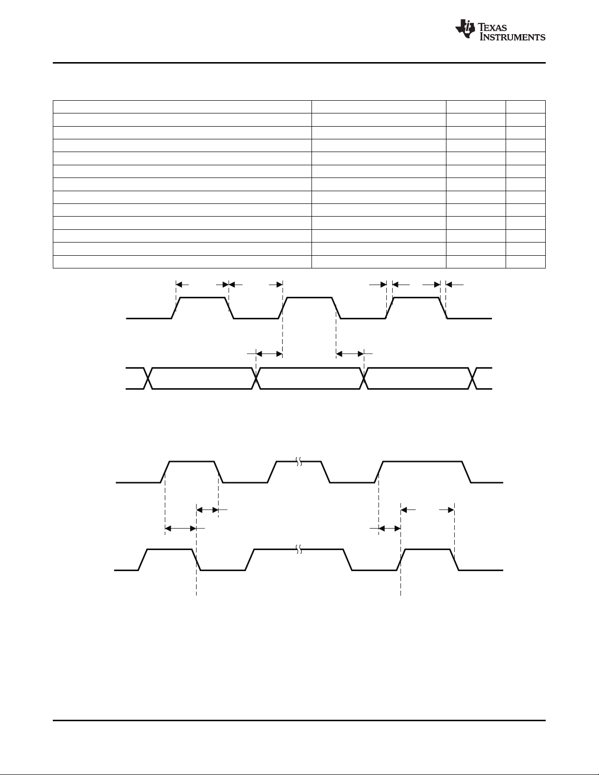
t
h1
t
su1
t
(edge)
t
su2
t
h2
SCLK
(Input)
LRCLK
(Input)
SDIN
T0026-04
t
r
t
f
TAS5711
www.ti.com
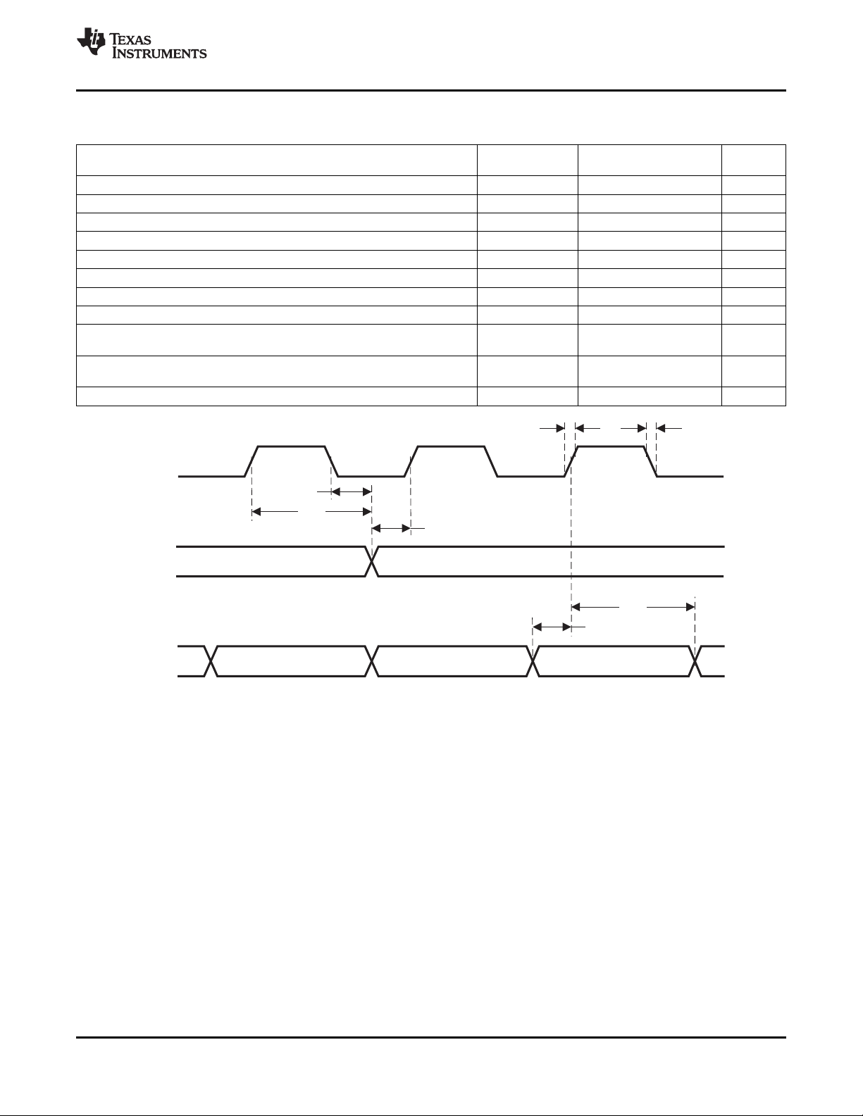
SERIAL AUDIO PORTS SLAVE MODE
over recommended operating conditions (unless otherwise noted)
PARAMETER MIN TYP MAX UNIT
f
SCLKIN
t
su1
t
h1
t
su2
t
h2
t
(edge)
tr/t
f
Frequency, SCLK 32 × fS, 48 × fS, 64 × f
S
Setup time, LRCLK to SCLK rising edge 10 ns
Hold time, LRCLK from SCLK rising edge 10 ns
Setup time, SDIN to SCLK rising edge 10 ns
Hold time, SDIN from SCLK rising edge 10 ns
LRCLK frequency 8 48 48 kHz
SCLK duty cycle 40% 50% 60%
LRCLK duty cycle 40% 50% 60%
SCLK rising edges between LRCLK rising edges 32 64
LRCLK clock edge with respect to the falling edge of SCLK –1/4 1/4
Rise/fall time for SCLK/LRCLK 8 ns
SLOS600 –DECEMBER 2009
TEST
CONDITIONS
CL= 30 pF 1.024 12.288 MHz
SCLK
edges
SCLK
period
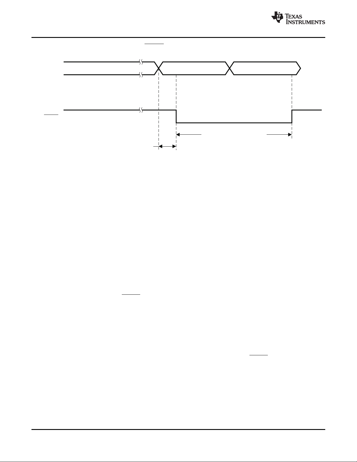
Figure 2. Slave Mode Serial Data Interface Timing
Copyright © 2009, Texas Instruments Incorporated Submit Documentation Feedback 11
Product Folder Link(s): TAS5711
Page 12
SCL
SDA
t
w(H)
t
w(L)
t
r
t
f
t
su1
t
h1
T0027-01
SCL
SDA
t
h2
t
(buf)
t
su2
t
su3
Start
Condition
Stop
Condition
T0028-01
TAS5711
SLOS600 –DECEMBER 2009
I2C SERIAL CONTROL PORT OPERATION
Timing characteristics for I2C Interface signals over recommended operating conditions (unless otherwise noted)
PARAMETER TEST CONDITIONS MIN MAX UNIT
f
t
t
t
t
t
t
t
t
t
t
C
SCL
w(H)
w(L)
r
f
su1
h1
(buf)
su2
h2
su3
Frequency, SCL No wait states 400 kHz
Pulse duration, SCL high 0.6 μs
Pulse duration, SCL low 1.3 μs
Rise time, SCL and SDA 300 ns
Fall time, SCL and SDA 300 ns
Setup time, SDA to SCL 100 ns
Hold time, SCL to SDA 0 ns
Bus free time between stop and start condition 1.3 μs
Setup time, SCL to start condition 0.6 μs
Hold time, start condition to SCL 0.6 μs
Setup time, SCL to stop condition 0.6 μs
Load capacitance for each bus line 400 pF
L
www.ti.com
Figure 3. SCL and SDA Timing
Figure 4. Start and Stop Conditions Timing
12 Submit Documentation Feedback Copyright © 2009, Texas Instruments Incorporated
Product Folder Link(s): TAS5711
Page 13
t
w(RESET)
RESET
t
d(I2C_ready)
SystemInitialization.
EnableviaI C.
2
T0421-01
I C Active
2
I C Active
2
TAS5711
www.ti.com
SLOS600 –DECEMBER 2009
RESET TIMING (RESET)
Control signal parameters over recommended operating conditions (unless otherwise noted). Please refer to Recommended
Use Model section on usage of all terminals.
PARAMETER MIN TYP MAX UNIT
t
w(RESET)
t
d(I2C_ready)
NOTES: On power up, it is recommended that the TAS5711 RESET be held LOW for at least 100 μs after DVDD has
reached 3 V.
If the RESET is asserted LOW while PDN is LOW, then the RESET must continue to be held LOW for at least 100 μs
after PDN is deasserted (HIGH).
Pulse duration, RESET active 100 µs
Time to enable I2C 12.0 ms
Figure 5. Reset Timing
Copyright © 2009, Texas Instruments Incorporated Submit Documentation Feedback 13
Product Folder Link(s): TAS5711
Page 14
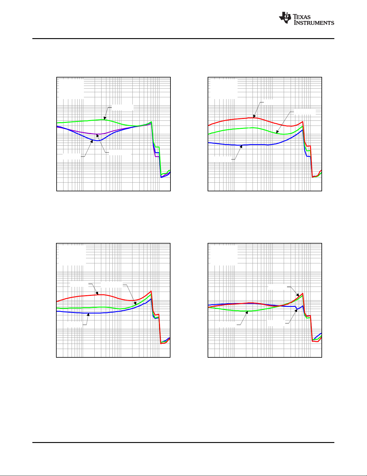
Frequency (Hz)
THD+N (%)
TOTAL HARMONIC DISTORTION + NOISE
vs
FREQUENCY
0.001
0.01
0.1
1
10
20 100 1k 10k 20k
PO = 0.5W
PO = 1W
PO = 2.5W
G001
PVDD = 8V
RL = 8Ω
TA = 25°C
Frequency (Hz)
THD+N (%)
TOTAL HARMONIC DISTORTION + NOISE
vs
FREQUENCY
0.001
0.01
0.1
1
10
20 100 1k 10k 20k
PO = 1W
PO = 2.5W
PO = 5W
G002
PVDD = 12V
RL = 8Ω
TA = 25°C
Frequency (Hz)
THD+N (%)
TOTAL HARMONIC DISTORTION + NOISE
vs
FREQUENCY
0.001
0.01
0.1
1
10
20 100 1k 10k 20k
PO = 1W
PO = 2.5W
PO = 5W
G003
PVDD = 18V
RL = 8Ω
TA = 25°C
Frequency (Hz)
THD+N (%)
TOTAL HARMONIC DISTORTION + NOISE
vs
FREQUENCY
0.001
0.01
0.1
1
10
20 100 1k 10k 20k
PO = 1W
PO = 2.5W
PO = 5W
G004
PVDD = 24V
RL = 8Ω
TA = 25°C
TAS5711
SLOS600 –DECEMBER 2009
www.ti.com
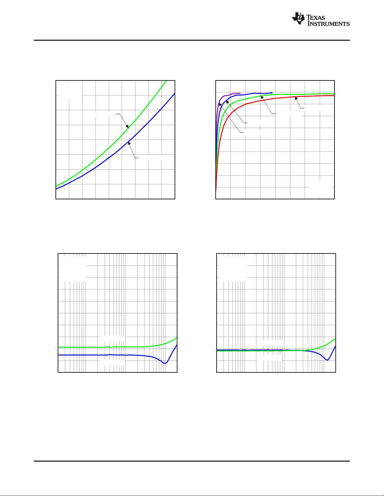
TYPICAL CHARACTERISTICS, BTL CONFIGURATION
Figure 6. Figure 7.
Figure 8. Figure 9.
14 Submit Documentation Feedback Copyright © 2009, Texas Instruments Incorporated
Product Folder Link(s): TAS5711
Page 15
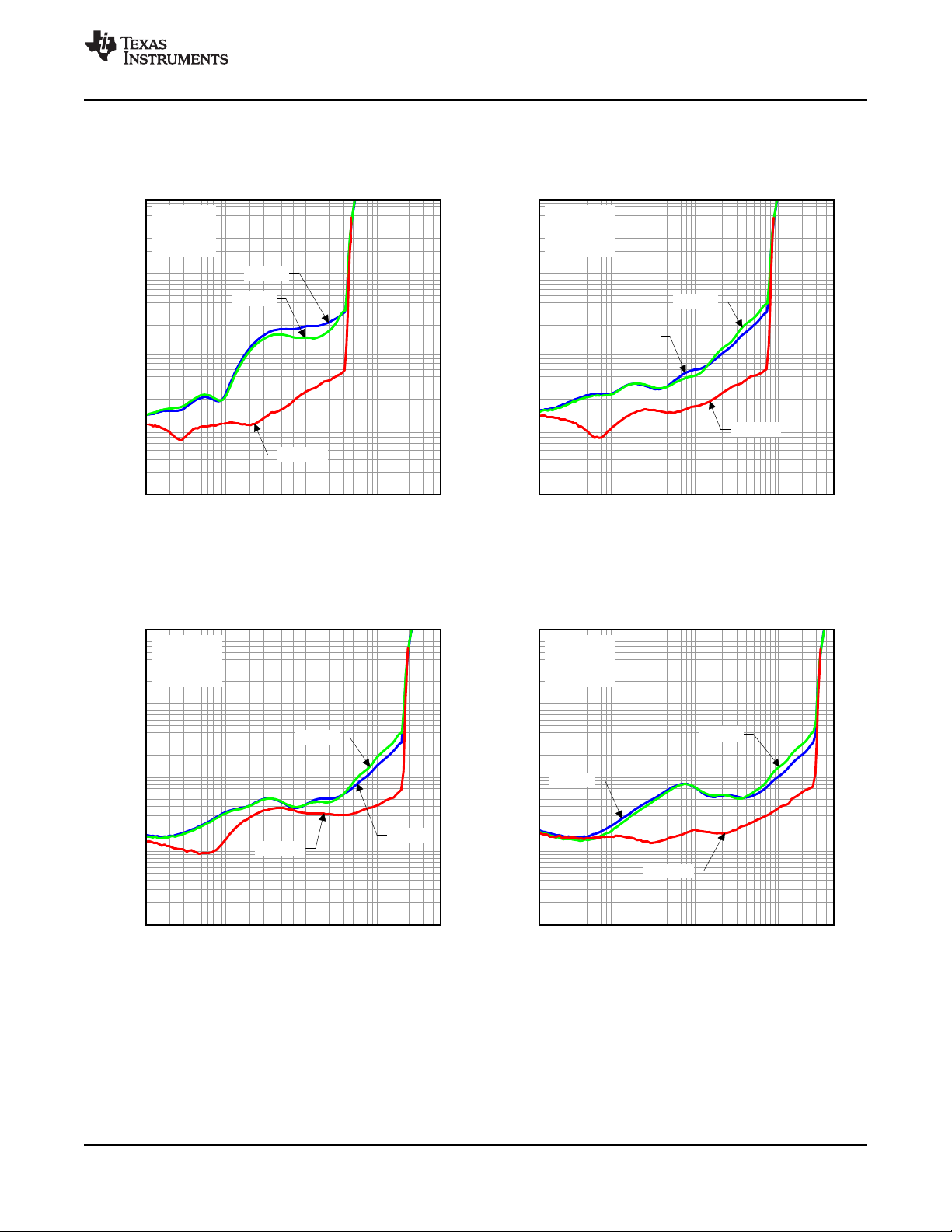
Output Power (W)
THD+N (%)
TOTAL HARMONIC DISTORTION + NOISE
vs
OUTPUT POWER
0.01 0.1 1 10 50
0.001
0.01
0.1
1
10
f = 20Hz
f = 1kHz
f = 10kHz
G005
PVDD = 8V
RL = 8Ω
TA = 25°C
Output Power (W)
THD+N (%)
TOTAL HARMONIC DISTORTION + NOISE
vs
OUTPUT POWER
0.01 0.1 1 10 50
0.001
0.01
0.1
1
10
f = 20Hz
f = 1kHz
f = 10kHz
G006
PVDD = 12V
RL = 8Ω
TA = 25°C
Output Power (W)
THD+N (%)
TOTAL HARMONIC DISTORTION + NOISE
vs
OUTPUT POWER
0.01 0.1 1 10 50
0.001
0.01
0.1
1
10
f = 20Hz
f = 1kHz
f = 10kHz
G007
PVDD = 18V
RL = 8Ω
TA = 25°C
Output Power (W)
THD+N (%)
TOTAL HARMONIC DISTORTION + NOISE
vs
OUTPUT POWER
0.01 0.1 1 10 50
0.001
0.01
0.1
1
10
f = 20Hz
f = 1kHz
f = 10kHz
G008
PVDD = 24V
RL = 8Ω
TA = 25°C
TAS5711
www.ti.com
SLOS600 –DECEMBER 2009
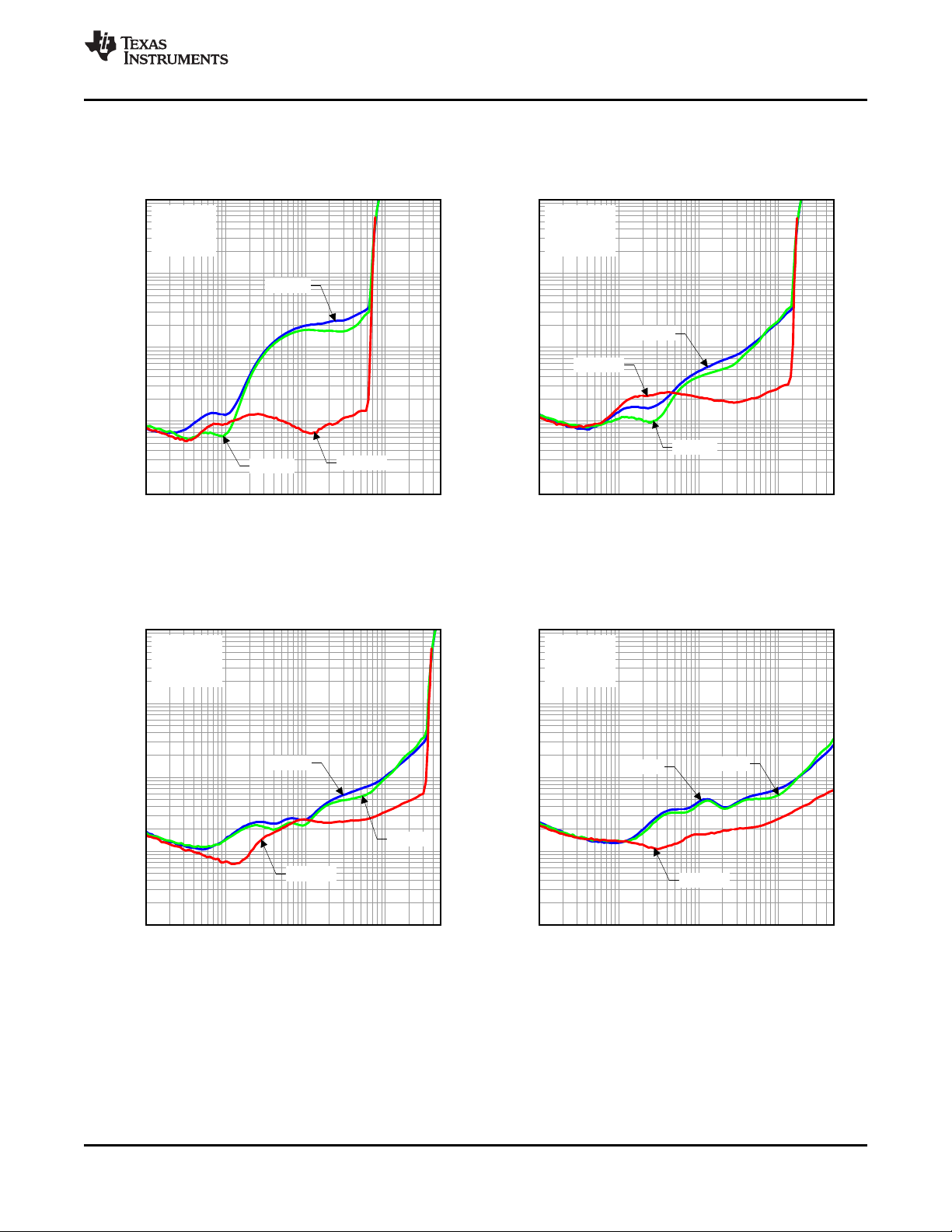
TYPICAL CHARACTERISTICS, BTL CONFIGURATION (continued)
Figure 10. Figure 11.
Figure 12. Figure 13.
Copyright © 2009, Texas Instruments Incorporated Submit Documentation Feedback 15
Product Folder Link(s): TAS5711
Page 16
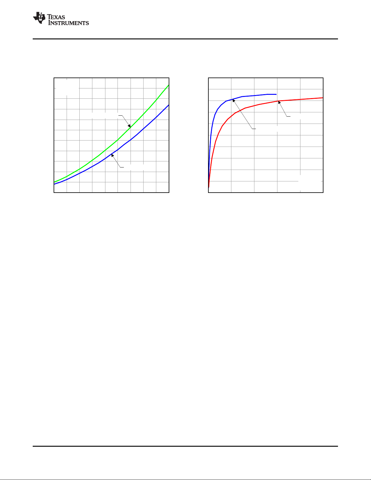
Supply Voltage (V)
Output Power (W)
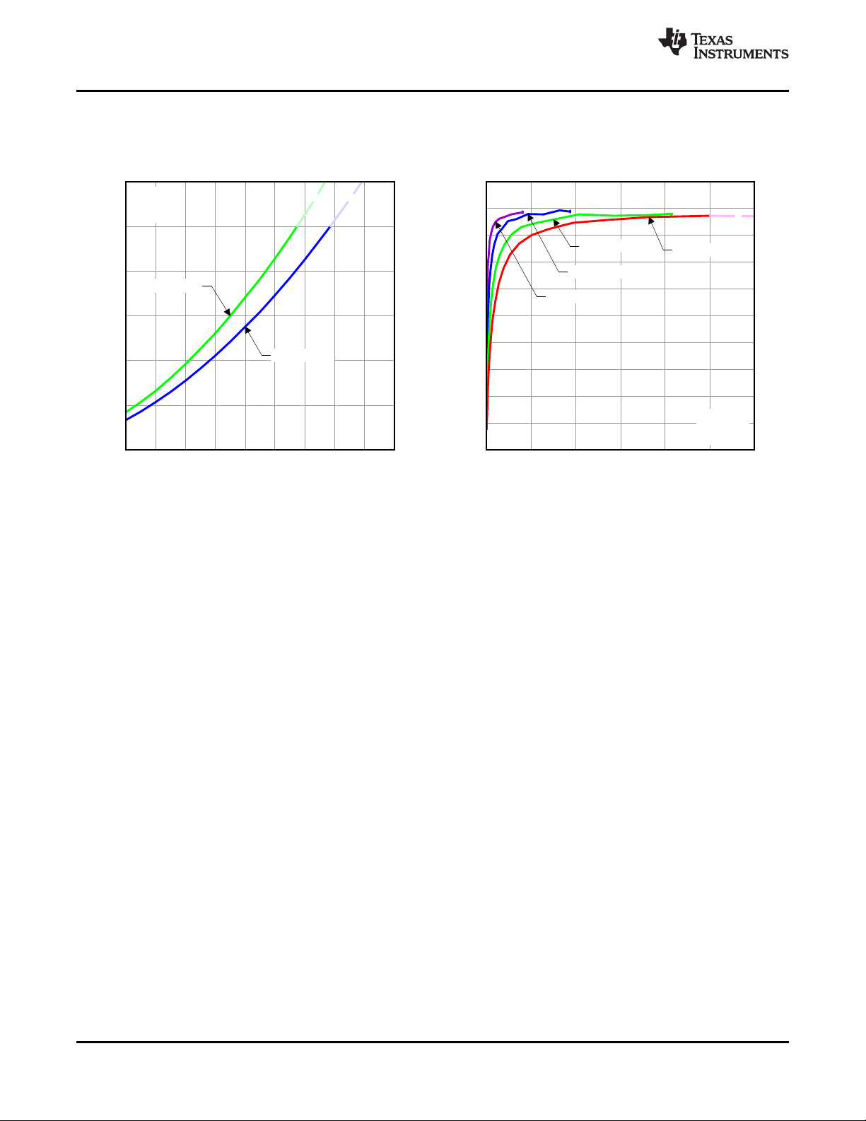
OUTPUT POWER
vs
SUPPLY VOLTAGE
8 10 12 14 16 18 20 22 24 26
0
5
10
15
20
25
30
35
40
THD+N = 1%
THD+N = 10%
G009
RL = 8Ω
TA = 25°C
Total Output Power (W)
Efficiency (%)
EFFICIENCY
vs
TOTAL OUTPUT POWER
0 5 10 15 20 25 30 35 40
0
10
20
30
40
50
60
70
80
90
100
PVDD = 8V
PVDD = 12V
PVDD = 18V
PVDD = 24V
G010
RL = 8Ω
TA = 25°C
Frequency (Hz)
Crosstalk (dB)
CROSSTALK
vs
FREQUENCY
-100
-90
-80
-70
-60
-50
-40
-30
-20
-10
0
20 100 1k 10k 20k
Left to Right
Right to Left
G011
PO = 1W
PVDD = 8V
RL = 8Ω
TA = 25°C
Frequency (Hz)
Crosstalk (dB)
CROSSTALK
vs
FREQUENCY
-100
-90
-80
-70
-60
-50
-40
-30
-20
-10
0
20 100 1k 10k 20k
Left to Right
Right to Left
G012
PO = 1W
PVDD = 12V
RL = 8Ω
TA = 25°C
TAS5711
SLOS600 –DECEMBER 2009
TYPICAL CHARACTERISTICS, BTL CONFIGURATION (continued)
www.ti.com
Figure 14. Figure 15.
Figure 16. Figure 17.
16 Submit Documentation Feedback Copyright © 2009, Texas Instruments Incorporated
Product Folder Link(s): TAS5711
Page 17
Frequency (Hz)
Crosstalk (dB)
CROSSTALK
vs
FREQUENCY
-100
-90
-80
-70
-60
-50
-40
-30
-20
-10
0
20 100 1k 10k 20k
Left to Right
Right to Left
G013
PO = 1W
PVDD = 18V
RL = 8Ω
TA = 25°C
Frequency (Hz)
Crosstalk (dB)
CROSSTALK
vs
FREQUENCY
-100
-90
-80
-70
-60
-50
-40
-30
-20
-10
0
20 100 1k 10k 20k
Left to Right
Right to Left
G014
PO = 1W
PVDD = 24V
RL = 8Ω
TA = 25°C
TAS5711
www.ti.com
SLOS600 –DECEMBER 2009
TYPICAL CHARACTERISTICS, BTL CONFIGURATION (continued)
Figure 18. Figure 19.
Copyright © 2009, Texas Instruments Incorporated Submit Documentation Feedback 17
Product Folder Link(s): TAS5711
Page 18
Frequency (Hz)
THD+N (%)
TOTAL HARMONIC DISTORTION + NOISE
vs
FREQUENCY
0.001
0.01
0.1
1
10
20 100 1k 10k 20k
PO = 0.5W
PO = 1W
PO = 2.5W
G015
PVDD = 12V
RL = 4Ω
TA = 25°C
Frequency (Hz)
THD+N (%)
TOTAL HARMONIC DISTORTION + NOISE
vs
FREQUENCY
0.001
0.01
0.1
1
10
20 100 1k 10k 20k
PO = 1W
PO = 2.5W
PO = 5W
G016
PVDD = 18V
RL = 4Ω
TA = 25°C
Frequency (Hz)
THD+N (%)
TOTAL HARMONIC DISTORTION + NOISE
vs
FREQUENCY
0.001
0.01
0.1
1
10
20 100 1k 10k 20k
PO = 1W
PO = 2.5W
PO = 5W
G017
PVDD = 24V
RL = 4Ω
TA = 25°C
Output Power (W)
THD+N (%)
TOTAL HARMONIC DISTORTION + NOISE
vs
OUTPUT POWER
0.01 0.1 1 10 50
0.001
0.01
0.1
1
10
PVDD = 12V
PVDD = 18V
PVDD = 24V
G018
f = 1kHz
RL = 4Ω
TA = 25°C
TAS5711
SLOS600 –DECEMBER 2009
www.ti.com
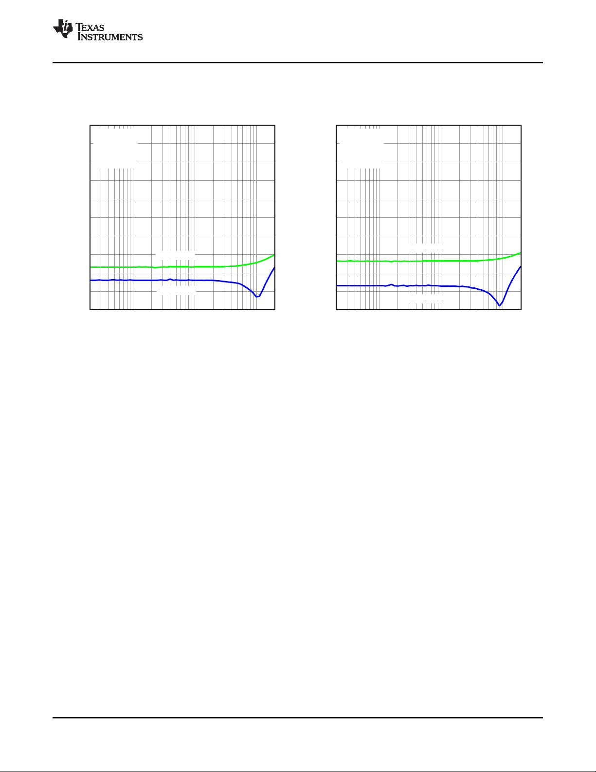
TYPICAL CHARACTERISTICS, SE CONFIGURATION
Figure 20. Figure 21.
Figure 22. Figure 23.
18 Submit Documentation Feedback Copyright © 2009, Texas Instruments Incorporated
Product Folder Link(s): TAS5711
Page 19
Supply Voltage (V)
Output Power (W)
OUTPUT POWER
vs
SUPPLY VOLTAGE
8 10 12 14 16 18 20 22 24 26
0
2
4
6
8
10
12
14
16
18
20
22
THD+N = 1%
THD+N = 10%
G019
RL = 4Ω
TA = 25°C
Total Output Power (W)
Efficiency (%)
EFFICIENCY
vs
TOTAL OUTPUT POWER
0 3 6 9 12 15
0
10
20
30
40
50
60
70
80
90
100
PVDD = 12V
PVDD = 24V
G020
RL = 4Ω
TA = 25°C
TAS5711
www.ti.com
SLOS600 –DECEMBER 2009
TYPICAL CHARACTERISTICS, SE CONFIGURATION (continued)
Figure 24. Figure 25.
Copyright © 2009, Texas Instruments Incorporated Submit Documentation Feedback 19
Product Folder Link(s): TAS5711
Page 20
Frequency (Hz)
THD+N (%)
TOTAL HARMONIC DISTORTION + NOISE
vs
FREQUENCY
0.001
0.01
0.1
1
10
20 100 1k 10k 20k
PO = 1W
PO = 2W
PO = 5W
G021
PVDD = 8V
RL = 4Ω
TA = 25°C
Frequency (Hz)
THD+N (%)
TOTAL HARMONIC DISTORTION + NOISE
vs
FREQUENCY
0.001
0.01
0.1
1
10
20 100 1k 10k 20k
PO = 1W
PO = 2W
PO = 5W
G022
PVDD = 12V
RL = 4Ω
TA = 25°C
Frequency (Hz)
THD+N (%)
TOTAL HARMONIC DISTORTION + NOISE
vs
FREQUENCY
0.001
0.01
0.1
1
10
20 100 1k 10k 20k
PO = 1W
PO = 2W
PO = 5W
G023
PVDD = 18V
RL = 4Ω
TA = 25°C
Frequency (Hz)
THD+N (%)
TOTAL HARMONIC DISTORTION + NOISE
vs
FREQUENCY
0.001
0.01
0.1
1
10
20 100 1k 10k 20k
PO = 1W
PO = 2W
PO = 5W
G024
PVDD = 24V
RL = 4Ω
TA = 25°C
TAS5711
SLOS600 –DECEMBER 2009
www.ti.com
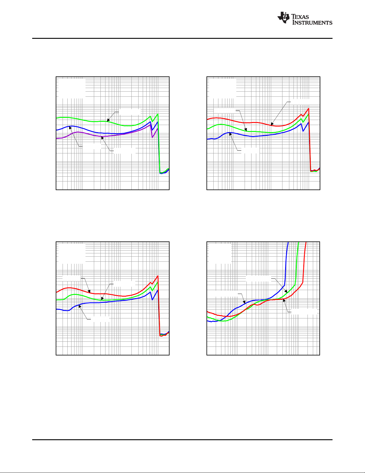
TYPICAL CHARACTERISTICS, PBTL CONFIGURATION
Figure 26. Figure 27.
Figure 28. Figure 29.
20 Submit Documentation Feedback Copyright © 2009, Texas Instruments Incorporated
Product Folder Link(s): TAS5711
Page 21
Output Power (W)
THD+N (%)
TOTAL HARMONIC DISTORTION + NOISE
vs
OUTPUT POWER
0.01 0.1 1 10 50
0.001
0.01
0.1
1
10
f = 20Hz
f = 1kHz
f = 10kHz
G025
PVDD = 8V
RL = 4Ω
TA = 25°C
Output Power (W)
THD+N (%)
TOTAL HARMONIC DISTORTION + NOISE
vs
OUTPUT POWER
0.01 0.1 1 10 50
0.001
0.01
0.1
1
10
f = 20Hz
f = 1kHz
f = 10kHz
G026
PVDD = 12V
RL = 4Ω
TA = 25°C
Output Power (W)
THD+N (%)
TOTAL HARMONIC DISTORTION + NOISE
vs
OUTPUT POWER
0.01 0.1 1 10 50
0.001
0.01
0.1
1
10
f = 20Hz
f = 1kHz
f = 10kHz
G027
PVDD = 18V
RL = 4Ω
TA = 25°C
Output Power (W)
THD+N (%)
TOTAL HARMONIC DISTORTION + NOISE
vs
OUTPUT POWER
0.01 0.1 1 10 50
0.001
0.01
0.1
1
10
f = 20Hz
f = 1kHz
f = 10kHz
G028
PVDD = 24V
RL = 4Ω
TA = 25°C
TAS5711
www.ti.com
SLOS600 –DECEMBER 2009
TYPICAL CHARACTERISTICS, PBTL CONFIGURATION (continued)
Figure 30. Figure 31.
Figure 32. Figure 33.
Copyright © 2009, Texas Instruments Incorporated Submit Documentation Feedback 21
Product Folder Link(s): TAS5711
Page 22
Supply Voltage (V)
Output Power (W)
OUTPUT POWER
vs
SUPPLY VOLTAGE
8 10 12 14 16 18 20 22 24 26
0
10
20
30
40
50
60
THD+N = 1%
THD+N = 10%
G029
RL = 4Ω
TA = 25°C
Total Output Power (W)
Efficiency (%)
EFFICIENCY
vs
TOTAL OUTPUT POWER
0 10 20 30 40 50 60
0
10
20
30
40
50
60
70
80
90
100
PVDD = 8V
PVDD = 12V
PVDD = 18V
PVDD = 24V
G030
RL = 4Ω
TA = 25°C
TAS5711
SLOS600 –DECEMBER 2009
TYPICAL CHARACTERISTICS, PBTL CONFIGURATION (continued)
NOTE: Dashed lines represent thermally limited regions. NOTE: Dashed line represents thermally limited region.
Figure 34. Figure 35.
www.ti.com
22 Submit Documentation Feedback Copyright © 2009, Texas Instruments Incorporated
Product Folder Link(s): TAS5711
Page 23
TAS5711
www.ti.com
SLOS600 –DECEMBER 2009
DETAILED DESCRIPTION
POWER SUPPLY
To facilitate system design, the TAS5711 needs only a 3.3-V supply in addition to the (typical) 18-V power-stage
supply. An internal voltage regulator provides suitable voltage levels for the gate drive circuitry. Additionally, all
circuitry requiring a floating voltage supply, e.g., the high-side gate drive, is accommodated by built-in bootstrap
circuitry requiring only a few external capacitors.
In order to provide good electrical and acoustical characteristics, the PWM signal path for the output stage is
designed as identical, independent half-bridges. For this reason, each half-bridge has separate bootstrap pins
(BST_x), and power-stage supply pins (PVDD_x). The gate drive voltages (GVDD_AB and GVDD_CD) are
derived from the PVDD voltage. Special attention should be paid to placing all decoupling capacitors as close to
their associated pins as possible. In general, inductance between the power-supply pins and decoupling
capacitors must be avoided.
For a properly functioning bootstrap circuit, a small ceramic capacitor must be connected from each bootstrap pin
(BST_x) to the power-stage output pin (OUT_x). When the power-stage output is low, the bootstrap capacitor is
charged through an internal diode connected between the gate-drive regulator output pin (GVDD_x) and the
bootstrap pin. When the power-stage output is high, the bootstrap capacitor potential is shifted above the output
potential and thus provides a suitable voltage supply for the high-side gate driver. In an application with PWM
switching frequencies in the range from 352 kHz to 384 kHz, it is recommended to use 33-nF 50-V X7R
capacitors, size 0603 or 0805, for the bootstrap supply. These 33-nF capacitors ensure sufficient energy storage,
even during minimal PWM duty cycles, to keep the high-side power stage FET (LDMOS) fully turned on during
the remaining part of the PWM cycle.
Special attention should be paid to the power-stage power supply; this includes component selection, PCB
placement, and routing. As indicated, each half-bridge has independent power-stage supply pins (PVDD_x). For
optimal electrical performance, EMC compliance, and system reliability, it is important that each PVDD_x pin is
decoupled with a 100-nF ceramic capacitor placed as close as possible to each supply pin.
The TAS5711 is fully protected against erroneous power-stage turnon due to parasitic gate charging.
ERROR REPORTING
The A_SEL pin has two functions: I2C device-address select and fault indication. On RESET, this pin is an input
and defines the I2C address. But this pin can be programmed after RESET to be an output by writing 1 to bit 0 of
I2C register 0x05. In that mode, the A_SEL pin has the definition shown in Table 1.
Any fault resulting in device shutdown is signaled by the A_SEL pin going low (see Table 1). A latched version of
this pin is available on D1 of register 0x02. The bit can be cleared only by an I2C write.
Table 1. FAULT Output States
FAULT DESCRIPTION
0 Overcurrent (OC) or undervoltage (UVP) error or overtemperature error (OTE) or over
1 No faults (normal operation)
voltage ERROR
Copyright © 2009, Texas Instruments Incorporated Submit Documentation Feedback 23
Product Folder Link(s): TAS5711
Page 24
FAULT
~300ns
ProgrammableRecovery Time
PowerStage
FaultState
FAULT
NO-FAULT NO-FAULT
T0450-01
TAS5711
SLOS600 –DECEMBER 2009
www.ti.com
Table 1. FAULT Output States (continued)
Figure 36. Fault Timing Diagram
DEVICE PROTECTION SYSTEM
Overcurrent (OC) Protection With Current Limiting
The device has independent, fast-reacting current detectors on all high-side and low-side power-stage FETs. The
detector outputs are closely monitored by two protection systems. The first protection system controls the power
stage in order to prevent the output current further increasing, i.e., it performs a cycle-by-cycle current-limiting
function, rather than prematurely shutting down during combinations of high-level music transients and extreme
speaker load impedance drops. If the high-current condition situation persists, i.e., the power stage is being
overloaded, a second protection system triggers a latching shutdown, resulting in the power stage being set in
the high-impedance (Hi-Z) state. The device returns to normal operation once the fault condition (i.e., a short
circuit on the output) is removed. Current limiting and overcurrent protection are not independent for half-bridges.
That is, if the bridge-tied load between half-bridges A and B causes an overcurrent fault, half-bridges A, B, C,
and D are shut down.
Overtemperature Protection
The TAS5711 has over temperature-protection system. If the device junction temperature exceeds 150°C
(nominal), the device is put into thermal shutdown, resulting in all half-bridge outputs being set in the
high-impedance (Hi-Z) state and FAULT being asserted low. The TAS5711 recovers automatically once the
temperature drops approximately 30°.
Undervoltage Protection (UVP) and Power-On Reset (POR)
The UVP and POR circuits of the TAS5711 fully protect the device in any power-up/down and brownout situation.
While powering up, the POR circuit resets the overload circuit and ensures that all circuits are fully operational
when the PVDD and AVDD supply voltages reach 7.6 V and 2.7 V, respectively. Although PVDD and AVDD are
independently monitored, a supply voltage drop below the UVP threshold on AVDD or either PVDD pin results in
all half-bridge outputs immediately being set in the high-impedance (Hi-Z) state and FAULT being asserted low.
24 Submit Documentation Feedback Copyright © 2009, Texas Instruments Incorporated
Product Folder Link(s): TAS5711
Page 25

TAS5711
www.ti.com
SLOS600 –DECEMBER 2009
SSTIMER FUNCTIONALITY
The SSTIMER pin uses a capacitor connected between this pin and ground to control the output duty cycle when
exiting all-channel shutdown. The capacitor on the SSTIMER pin is slowly charged through an internal current
source, and the charge time determines the rate at which the output transitions from a near zero duty cycle to the
desired duty cycle. This allows for a smooth transition that minimizes audible pops and clicks. When the part is
shutdown the drivers are tristated and transition slowly down through a 3K resistor, similarly minimizing pops and
clicks. The shutdown transition time is independent of SSTIMER pin capacitance. Larger capacitors will increase
the start-up time, while capacitors smaller than 2.2 nF will decrease the start-up time. The SSTIMER pin should
be left floating for BD modulation (BTL and PBTL modes) and in 2.1 mode.
CLOCK, AUTO DETECTION, AND PLL
The TAS5711 is a slave device. It accepts MCLK, SCLK, and LRCLK. The digital audio processor (DAP)
supports all the sample rates and MCLK rates that are defined in the clock control register .
The TAS5711 checks to verify that SCLK is a specific value of 32 fS, 48 fS, or 64 fS. The DAP only supports a 1 ×
fSLRCLK. The timing relationship of these clocks to SDIN is shown in subsequent sections. The clock section
uses MCLK or the internal oscillator clock (when MCLK is unstable, out of range, or absent) to produce the
internal clock (DCLK) running at 512 time the PWM switching frequency.
The DAP can autodetect and set the internal clock control logic to the appropriate settings for all supported clock
rates as defined in the clock control register.
TAS5711 has robust clock error handling that uses the bulit-in trimmed oscillator clock to quickly detect
changes/errors. Once the system detects a clock change/error, it will mute the audio (through a single step mute)
and then force PLL to limp using the internal oscillator as a reference clock. Once the clocks are stable, the
system will auto detect the new rate and revert to normal operation. During this process, the default volume will
be restored in a single step (also called hard unmute). The ramp process can be programmed to ramp back
slowly (also called soft unmute) as defined in volume register (0x0E).
SERIAL DATA INTERFACE
Serial data is input on SDIN. The PWM outputs are derived from SDIN. The TAS5711 DAP accepts serial data in
16-, 20-, or 24-bit left-justified, right-justified, and I2S serial data formats.
PWM Section
The TAS5711 DAP device uses noise-shaping and sophisticated non-linear correction algorithms to achieve high
power efficiency and high-performance digital audio reproduction. The DAP uses a fourth-order noise shaper to
increase dynamic range and SNR in the audio band. The PWM section accepts 24-bit PCM data from the DAP
and outputs two BTL PWM audio output channels.
The PWM section has individual channel dc blocking filters that can be enabled and disabled. The filter cutoff
frequency is less than 1 Hz. Individual channel de-emphasis filters for 44.1- and 48-kHz are included and can be
enabled and disabled.
Finally, the PWM section has an adjustable maximum modulation limit of 93.8% to 99.2%.
For detailed description of using audio processing features like DRC, EQ, 3D, and Bass Boost, please refer to
User's Guide and TAS570X GDE software development tool documentation. Also refer to GDE software
development tool for device data path.
SERIAL INTERFACE CONTROL AND TIMING
The I2S mode is set by writing to register 0x04.
I2S Timing
I2S timing uses LRCLK to define when the data being transmitted is for the left channel and when it is for the
right channel. LRCLK is low for the left channel and high for the right channel. A bit clock running at 32, 48, or
64 × fSis used to clock in the data. There is a delay of one bit clock from the time the LRCLK signal changes
state to the first bit of data on the data lines. The data is written MSB first and is valid on the rising edge of bit
clock. The DAP masks unused trailing data bit positions.
Copyright © 2009, Texas Instruments Incorporated Submit Documentation Feedback 25
Product Folder Link(s): TAS5711
Page 26

23
22
SCLK
32Clks
LRCLK(NoteReversedPhase)
LeftChannel
24-BitMode
1
19 18
20-BitMode
16-BitMode
15
14
MSB LSB
32Clks
RightChannel
2-ChannelI S(PhilipsFormat)StereoInput
2
T0034-01
5
4
9 8
1
0
0
4
5
1
0
23
22 1
19 18
15
14
MSB LSB
5
4
9 8
1
0
0
4
5
1
0
SCLK
23
22
SCLK
24Clks
LRCLK
LeftChannel
24-BitMode
1
19 18
20-BitMode
16-BitMode
15
14
MSB LSB
24Clks
RightChannel
2-ChannelI S(PhilipsFormat)StereoInput/Output(24-Bit TransferWordSize)
2
T0092-01
3
2
5
4
9 8
17
16
1
0
0
4
5
13
12
1
09 8
23
22
SCLK
1
19 18
15
14
MSB LSB
3
2
5
4
9 8
17
16
1
0
4
5
13
12
1
09 8
TAS5711
SLOS600 –DECEMBER 2009
www.ti.com
NOTE: All data presented in 2s-complement form with MSB first.
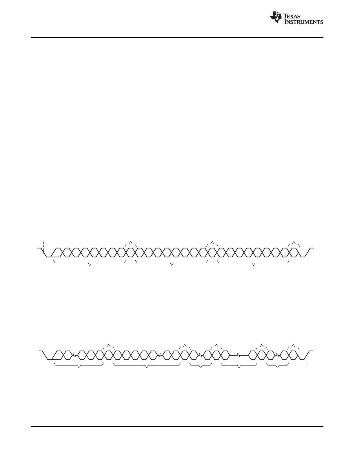
Figure 37. I2S 64-fSFormat
26 Submit Documentation Feedback Copyright © 2009, Texas Instruments Incorporated
NOTE: All data presented in 2s-complement form with MSB first.
Figure 38. I2S 48-fSFormat
Product Folder Link(s): TAS5711
Page 27

SCLK
16Clks
LRCLK
LeftChannel
16-BitMode
1 1
15 15
14 14
MSB LSB
16Clks
RightChannel
2-ChannelI S(PhilipsFormat)StereoInput
2
T0266-01
3 3
2 2
5 5
4 4
9 98 80
13 13
10 10
11 1112 12
SCLK
MSB LSB
23
22
SCLK
32Clks
LRCLK
LeftChannel
24-BitMode
1
19 18
20-BitMode
16-BitMode
15
14
MSB LSB
32Clks
RightChannel
2-ChannelLeft-JustifiedStereoInput
T0034-02
4
5
9 8
1
4
5
1
0
0
0
23
22 1
19 18
15
14
MSB LSB
4
5
9 8
1
4
5
1
0
0
0
SCLK
TAS5711
www.ti.com
NOTE: All data presented in 2s-complement form with MSB first.
SLOS600 –DECEMBER 2009
Figure 39. I2S 32-fSFormat
Left-Justified
Left-justified (LJ) timing uses LRCLK to define when the data being transmitted is for the left channel and when it
is for the right channel. LRCLK is high for the left channel and low for the right channel. A bit clock running at 32,
48, or 64 × fSis used to clock in the data. The first bit of data appears on the data lines at the same time LRCLK
toggles. The data is written MSB first and is valid on the rising edge of the bit clock. The DAP masks unused
trailing data bit positions.
NOTE: All data presented in 2s-complement form with MSB first.
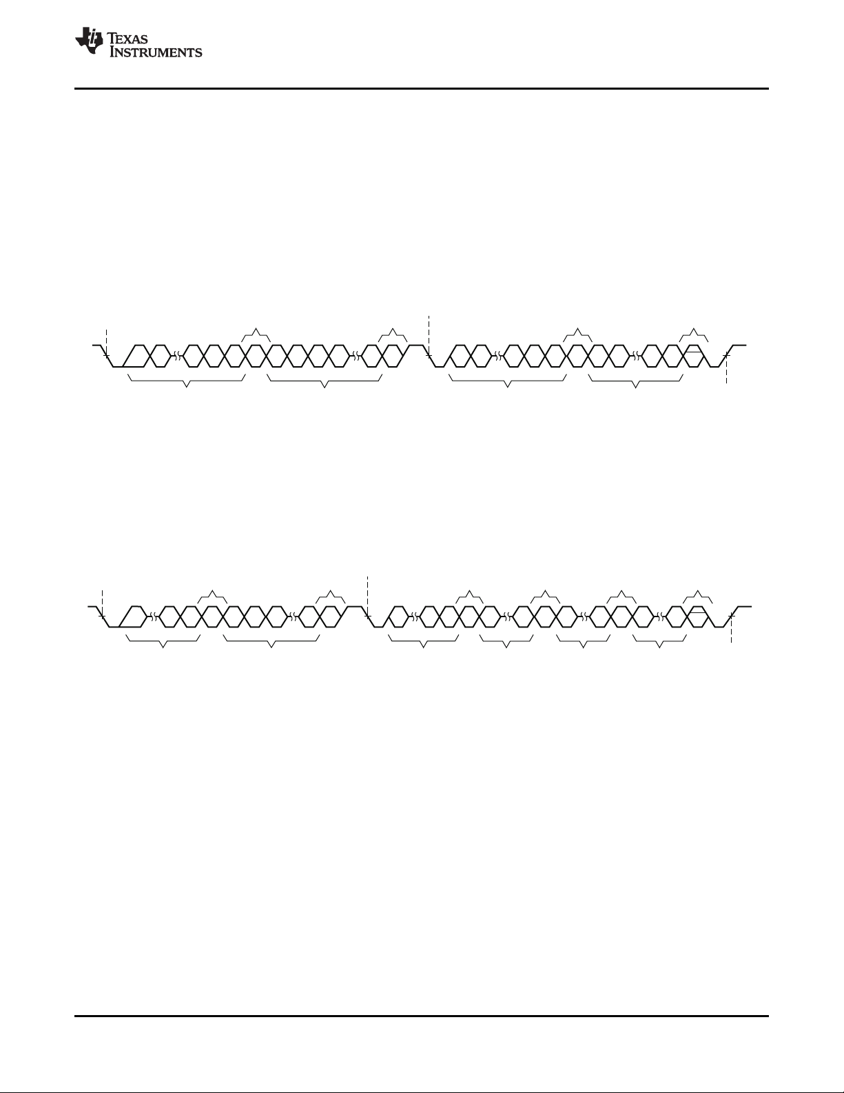
Figure 40. Left-Justified 64-fSFormat
Copyright © 2009, Texas Instruments Incorporated Submit Documentation Feedback 27
Product Folder Link(s): TAS5711
Page 28

23
22
SCLK
24Clks
LRCLK
LeftChannel
24-BitMode
1
19 18
20-BitMode
16-BitMode
15
14
MSB LSB
24Clks
RightChannel
2-ChannelLeft-JustifiedStereoInput(24-Bit TransferWordSize)
T0092-02
4
5
9 8
17
16
1
4
5
13
12
1
9 8
0
0
0
21
17
13
23
22
SCLK
1
19 18
15
14
MSB LSB
4
5
9 8
17
16
1
4
5
13
12
1
9 8
0
0
0
21
17
13
SCLK
16Clks
LRCLK
LeftChannel
16-BitMode
1 1
15 15
14 14
MSB LSB
16Clks
RightChannel
2-ChannelLeft-JustifiedStereoInput
T0266-02
3 3
2 2
5 5
4 4
9 98 80 0
13 13
10 10
11 1112 12
SCLK
MSB LSB
TAS5711
SLOS600 –DECEMBER 2009
www.ti.com
NOTE: All data presented in 2s-complement form with MSB first.
Figure 41. Left-Justified 48-fSFormat
NOTE: All data presented in 2s-complement form with MSB first.
Right-Justified
Right-justified (RJ) timing uses LRCLK to define when the data being transmitted is for the left channel and when
Figure 42. Left-Justified 32-fSFormat
28 Submit Documentation Feedback Copyright © 2009, Texas Instruments Incorporated
Product Folder Link(s): TAS5711
Page 29

23
22
SCLK
32Clks
LRCLK
LeftChannel
24-BitMode
1
20-BitMode
16-BitMode
15
14
MSB LSB
SCLK
32Clks
RightChannel
2-ChannelRight-Justified(SonyFormat)StereoInput
T0034-03
19 18
1
19 18
1
0
0
0
15
14
15
14
23
22 1
15
14
MSB LSB
19 18
1
19 18
1
0
0
0
15
14
15
14
TAS5711
www.ti.com
SLOS600 –DECEMBER 2009
it is for the right channel. LRCLK is high for the left channel and low for the right channel. A bit clock running at
32, 48, or 64 × fSis used to clock in the data. The first bit of data appears on the data 8 bit-clock periods (for
24-bit data) after LRCLK toggles. In RJ mode the LSB of data is always clocked by the last bit clock before
LRCLK transitions. The data is written MSB first and is valid on the rising edge of bit clock. The DAP masks
unused leading data bit positions.
Figure 43. Right Justified 64-fSFormat
Copyright © 2009, Texas Instruments Incorporated Submit Documentation Feedback 29
Product Folder Link(s): TAS5711
Page 30

23
22
SCLK
24Clks
LRCLK
LeftChannel
24-BitMode
1
20-BitMode
16-BitMode
15
14
MSB LSB
SCLK
24Clks
RightChannel
MSB
2-ChannelRight-JustifiedStereoInput(24-Bit TransferWordSize)
T0092-03
5
19 18
1
5
19 18
1
5
0
0
0
2
2
2
6
6
6
15
14
15
14
23
22 1
15
14
5
19 18
1
5
19 18
1
5
0
0
0
2
2
2
6
6
6
15
14
15
14
LSB
TAS5711
SLOS600 –DECEMBER 2009
www.ti.com
Figure 44. Right Justified 48-fSFormat
Figure 45. Right Justified 32-fSFormat
30 Submit Documentation Feedback Copyright © 2009, Texas Instruments Incorporated
Product Folder Link(s): TAS5711
Page 31

7-BitSlave Address
R/
W
8-BitRegister Address(N)
A
8-BitRegisterDataFor
Address(N)
Start Stop
SDA
SCL
7
6
5
4
3
2 1
0
7
6
5
4
3
2 1
0
7
6
5
4
3
2 1
0
7
6
5
4
3
2 1
0
A
8-BitRegisterDataFor
Address(N)
A A
T0035-01
TAS5711
www.ti.com
SLOS600 –DECEMBER 2009
I2C SERIAL CONTROL INTERFACE
The TAS5711 DAP has a bidirectional I2C interface that compatible with the I2C (Inter IC) bus protocol and
supports both 100-kHz and 400-kHz data transfer rates for single and multiple byte write and read operations.
This is a slave only device that does not support a multimaster bus environment or wait state insertion. The
control interface is used to program the registers of the device and to read device status.
The DAP supports the standard-mode I2C bus operation (100 kHz maximum) and the fast I2C bus operation
(400 kHz maximum). The DAP performs all I2C operations without I2C wait cycles.
General I2C Operation
The I2C bus employs two signals; SDA (data) and SCL (clock), to communicate between integrated circuits in a
system. Data is transferred on the bus serially one bit at a time. The address and data can be transferred in byte
(8-bit) format, with the most significant bit (MSB) transferred first. In addition, each byte transferred on the bus is
acknowledged by the receiving device with an acknowledge bit. Each transfer operation begins with the master
device driving a start condition on the bus and ends with the master device driving a stop condition on the bus.
The bus uses transitions on the data pin (SDA) while the clock is high to indicate a start and stop conditions. A
high-to-low transition on SDA indicates a start and a low-to-high transition indicates a stop. Normal data bit
transitions must occur within the low time of the clock period. These conditions are shown in Figure 46. The
master generates the 7-bit slave address and the read/write (R/W) bit to open communication with another
device and then waits for an acknowledge condition. The TAS5711 holds SDA low during the acknowledge clock
period to indicate an acknowledgment. When this occurs, the master transmits the next byte of the sequence.
Each device is addressed by a unique 7-bit slave address plus R/W bit (1 byte). All compatible devices share the
same signals via a bidirectional bus using a wired-AND connection. An external pullup resistor must be used for
the SDA and SCL signals to set the high level for the bus.
Figure 46. Typical I2C Sequence
There is no limit on the number of bytes that can be transmitted between start and stop conditions. When the last
word transfers, the master generates a stop condition to release the bus. A generic data transfer sequence is
shown in Figure 46.
Pin A_SEL defines the I2C device address. An external 15-kΩ pulldown on this pin gives a device address of
0x34 and a 15-kΩ pullup gives a device address of 0x36. The 7-bit address is 0011011 (0x36) or 0011010
(0x34).
I2C Device Address Change Procedure
• Write to device address change enable register, 0xF8 with a value of 0xF9 A5 A5 A5.
• Write to device register 0xF9 with a value of 0x0000 00XX, where XX is the new address.
• Any writes after that should use the new device address XX.
Single- and Multiple-Byte Transfers
The serial control interface supports both single-byte and multiple-byte read/write operations for subaddresses
0x00 to 0x1F. However, for the subaddresses 0x20 to 0xFF, the serial control interface supports only
multiple-byte read/write operations (in multiples of 4 bytes).
Copyright © 2009, Texas Instruments Incorporated Submit Documentation Feedback 31
Product Folder Link(s): TAS5711
Page 32
A6 A5 A4 A3 A2 A1 A0
R/W
ACK A7 A6 A5 A4 A3 A2 A1 A0 ACK D7 D6 D5 D4 D3 D2 D1 D0 ACK
Start
Condition
Stop
Condition
Acknowledge Acknowledge Acknowledge
I CDevice Addressand
2
Read/WriteBit
Subaddress DataByte
T0036-01
D7 D0 ACK
Stop
Condition
Acknowledge
I CDevice Addressand
2
Read/WriteBit
Subaddress LastDataByte
A6 A5 A1 A0 R/W ACK A7 A5 A1 A0 ACK D7 ACK
Start
Condition
Acknowledge Acknowledge Acknowledge
FirstDataByte
A4 A3A6
OtherDataBytes
ACK
Acknowledge
D0 D7 D0
T0036-02
TAS5711
SLOS600 –DECEMBER 2009
www.ti.com
During multiple-byte read operations, the DAP responds with data, a byte at a time, starting at the subaddress
assigned, as long as the master device continues to respond with acknowledges. If a particular subaddress does
not contain 32 bits, the unused bits are read as logic 0.
During multiple-byte write operations, the DAP compares the number of bytes transmitted to the number of bytes
that are required for each specific subaddress. For example, if a write command is received for a biquad
subaddress, the DAP expects to receive five 32-bit words. If fewer than five 32-bit data words have been
received when a stop command (or another start command) is received, the data received is discarded.
Supplying a subaddress for each subaddress transaction is referred to as random I2C addressing. The TAS5711
also supports sequential I2C addressing. For write transactions, if a subaddress is issued followed by data for
that subaddress and the 15 subaddresses that follow, a sequential I2C write transaction has taken place, and the
data for all 16 subaddresses is successfully received by the TAS5711. For I2C sequential write transactions, the
subaddress then serves as the start address, and the amount of data subsequently transmitted, before a stop or
start is transmitted, determines how many subaddresses are written. As was true for random addressing,
sequential addressing requires that a complete set of data be transmitted. If only a partial set of data is written to
the last subaddress, the data for the last subaddress is discarded. However, all other data written is accepted;
only the incomplete data is discarded.
Single-Byte Write
As shown in Figure 47, a single-byte data write transfer begins with the master device transmitting a start
condition followed by the I2C device address and the read/write bit. The read/write bit determines the direction of
the data transfer. For a write data transfer, the read/write bit will be a 0. After receiving the correct I2C device
address and the read/write bit, the DAP responds with an acknowledge bit. Next, the master transmits the
address byte or bytes corresponding to the TAS5711 internal memory address being accessed. After receiving
the address byte, the TAS5711 again responds with an acknowledge bit. Next, the master device transmits the
data byte to be written to the memory address being accessed. After receiving the data byte, the TAS5711 again
responds with an acknowledge bit. Finally, the master device transmits a stop condition to complete the
single-byte data write transfer.
Figure 47. Single-Byte Write Transfer
Multiple-Byte Write
A multiple-byte data write transfer is identical to a single-byte data write transfer except that multiple data bytes
are transmitted by the master device to the DAP as shown in Figure 48. After receiving each data byte, the
TAS5711 responds with an acknowledge bit.
Figure 48. Multiple-Byte Write Transfer
32 Submit Documentation Feedback Copyright © 2009, Texas Instruments Incorporated
Product Folder Link(s): TAS5711
Page 33
A6 A5 A0 R/W ACK A7 A6 A5 A4 A0 ACK A6 A5 A0 ACK
Start
Condition
Stop
Condition
Acknowledge Acknowledge Acknowledge
I CDevice Addressand
2
Read/WriteBit
Subaddress DataByte
D7 D6 D1 D0 ACK
I CDevice Addressand
Read/WriteBit
2
Not
Acknowledge
R/WA1 A1
RepeatStart
Condition
T0036-03
A6 A0 ACK
Acknowledge
I CDevice Addressand
Read/WriteBit
2
R/WA6 A0 R/W ACK A0 ACK D7 D0 ACK
Start
Condition
Stop
Condition
Acknowledge Acknowledge Acknowledge
LastDataByte
ACK
FirstDataByte
RepeatStart
Condition
Not
Acknowledge
I CDevice Addressand
Read/WriteBit
2
Subaddress OtherDataBytes
A7 A6 A5 D7 D0 ACK
Acknowledge
D7 D0
T0036-04
TAS5711
www.ti.com
SLOS600 –DECEMBER 2009
Single-Byte Read
As shown in Figure 49, a single-byte data read transfer begins with the master device transmitting a start
condition followed by the I2C device address and the read/write bit. For the data read transfer, both a write
followed by a read are actually done. Initially, a write is done to transfer the address byte or bytes of the internal
memory address to be read. As a result, the read/write bit becomes a 0. After receiving the TAS5711 address
and the read/write bit, TAS5711 responds with an acknowledge bit. In addition, after sending the internal memory
address byte or bytes, the master device transmits another start condition followed by the TAS5711 address and
the read/write bit again. This time the read/write bit becomes a 1, indicating a read transfer. After receiving the
address and the read/write bit, the TAS5711 again responds with an acknowledge bit. Next, the TAS5711
transmits the data byte from the memory address being read. After receiving the data byte, the master device
transmits a not acknowledge followed by a stop condition to complete the single byte data read transfer.
Figure 49. Single-Byte Read Transfer
Multiple-Byte Read
A multiple-byte data read transfer is identical to a single-byte data read transfer except that multiple data bytes
are transmitted by the TAS5711 to the master device as shown in Figure 50. Except for the last data byte, the
master device responds with an acknowledge bit after receiving each data byte.
Figure 50. Multiple Byte Read Transfer
Copyright © 2009, Texas Instruments Incorporated Submit Documentation Feedback 33
Product Folder Link(s): TAS5711
Page 34

CH1_audio
CH1_audio
CH1_audio
CH1_audio
CH2_audio
CH2_audio
CH3_audio
CH3_audio
CH2_audio
CH2_audio
PWM1
PWM1
PWM1
PWM1
PWM2
PWM2
PWM2
PWM2
PWM3
PWM3
PWM3
PWM3
PWM4
PWM4
PWM4
PWM4
2.0 BTL A D
0x20 (23) = 0
0x20 (19) = 0
0x05 (3) = X
0x05 (2) = 0
Reg set ti ng
2.0 BTL BD
0x20 (23) = 1
0x20 (19) = 1
0x05 (3) = X
0x05 (2) = 0
Reg set ti ng
2.1 SE, BTL- AD
0x20 (23) = 0
0x20 (19) = 0
0x05 (3) = 0
0x05 (2) = 1
Reg set ti ng
2.1 SE, BTL- BD
0x20 (23) = 0
0x20 (19) = 0
0x05 (3) = 1
0x05 (2) = 1
Reg set ti ng
A
A
A
A
B
B
B
B
C
C
C
C
D
D
D
D
B0378-01
TAS5711
SLOS600 –DECEMBER 2009
Output Mode and MUX Selection
www.ti.com
2.1-Mode Support
The TAS5711 uses a special mid-Z ramp sequence to reduce click and pop in SE-mode and 2.1-mode
operation.To enable the mid-Z ramp, register 0x05 bit D7 must be set to 1. To enable 2.1 mode, register 0x05 bit
D2 must be set to 1. The SSTIMER pin should be left floating in this mode.
Single-Filter PBTL-Mode Support
The TAS5711 supports parallel BTL (PBTL) mode with OUT_A/OUT_B (and OUT_C/OUT_D) connected before
the LC filter. In order to put the part in PBTL configuration, drive PBTL (pin 8) HIGH. This synchronizes the
turnoff of half-bridges A and B (and similarly C/D) if an overcurrent condition is detected in either half-bridge.
There is a pulldown resistor on the PBTL pin that configures the part in BTL mode if the pin is left floating.
PWM output multiplexers should be updated to set the device in PBTL mode. Output Mux Register (0x25) should
be written with a value of 0x01 10 32 45. Also, the PWM shutdown register (0x19) should be written with a value
of 0x3A.
Figure 51. Output Mode and MUX Selection
34 Submit Documentation Feedback Copyright © 2009, Texas Instruments Incorporated
Product Folder Link(s): TAS5711
Page 35
Output Level (dB)
Input Level (dB)
T
O
K
M0091-02
1:1 TransferFunction
Implemented TransferFunction
S
Z
–1
AlphaFilterStructure
w
a
B0265-01
Energy
Filter
a w,
T,K,O a wa,
a d d
/ ,a w
DRC1
DRC2
0x3A 0x40,0x41,0x42 0x3B/0x3C
0x3E/0x3F
0x43,0x44,0x45
0x3D
Compression
Control
Attack
and
Decay
Filters
AudioInput
DRCCoefficient
NOTE:
=1 –w α
TAS5711
www.ti.com
SLOS600 –DECEMBER 2009
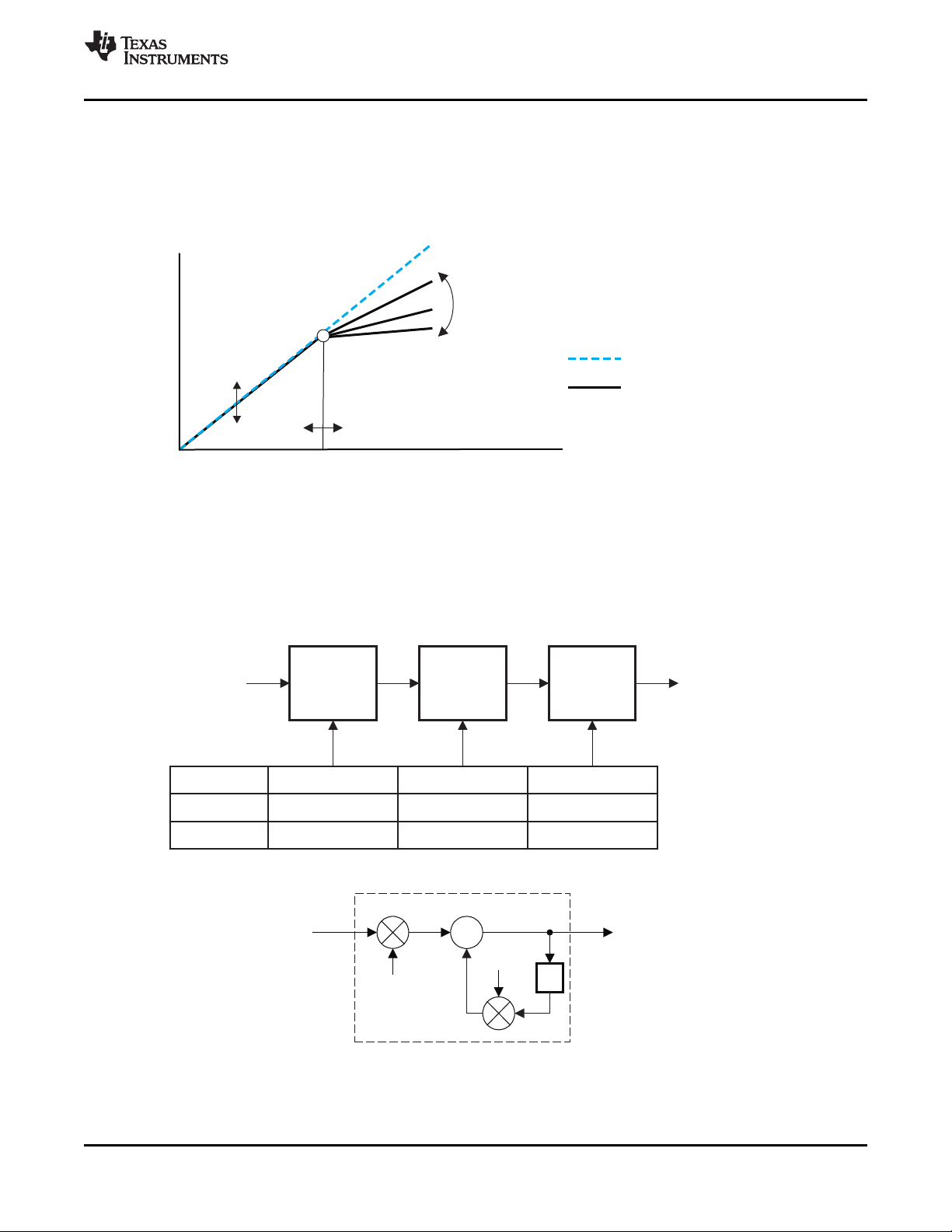
Dynamic Range Control (DRC)
The DRC scheme has a single threshold, offset, and slope (all programmable). There is one ganged DRC for the
left/right channels and one DRC for the subchannel.
The DRC input/output diagram is shown in Figure 52.
Refer to GDE software tool for more description on T, K, and O parameters.
Professional-quality dynamic range compression automatically adjusts volume to flatten volume level.
• Each DRC has adjustable threshold, offset, and compression levels
• Programmable energy, attack, and decay time constants
• Transparent compression: compressors can attack fast enough to avoid apparent clipping before engaging,
and decay times can be set slow enough to avoid pumping.
Figure 52. Dynamic Range Control
T = 9.23 format, all other DRC coefficients are 3.23 format
Copyright © 2009, Texas Instruments Incorporated Submit Documentation Feedback 35
Figure 53. DRC Structure
Product Folder Link(s): TAS5711
Page 36

2 Bit
–23
S_xx.xxxx_xxxx_xxxx_xxxx_xxxx_xxx
2 Bit
–5
2 Bit
–1
2 Bit
0
SignBit
2 Bit
1
M0125-01
TAS5711
SLOS600 –DECEMBER 2009
www.ti.com
BANK SWITCHING
The TAS5711 uses an approach called bank switching together with automatic sample-rate detection. All
processing features that must be changed for different sample rates are stored internally in three banks. The
user can program which sample rates map to each bank. By default, bank 1 is used in 32kHz mode, bank 2 is
used in 44.1/48 kHz mode, and bank 3 is used for all other rates. Combined with the clock-rate autodetection
feature, bank switching allows the TAS5711 to detect automatically a change in the input sample rate and switch
to the appropriate bank without any MCU intervention.
An external controller configures bankable locations (0x29-0x36, 0x3A-0x3F, and 0x58-0x5F) for all three banks
during the initialization sequence.
If auto bank switching is enabled (register 0x50, bits 2:0) , then the TAS5711 automatically swaps the coefficients
for subsequent sample rate changes, avoiding the need for any external controller intervention for a sample rate
change.
By default, bits 2:0 have the value 000; indicating that bank switching is disabled. In that state, updates to
bankable locations take immediate effect. A write to register 0x50 with bits 2:0 being 001, 010, or 011 brings the
system into the coefficient-bank-update state update bank1, update bank2, or update bank3, respectively. Any
subsequent write to bankable locations updates the coefficient banks stored outside the DAP. After updating all
the three banks, the system controller should issue a write to register 0x50 with bits 2:0 being 100; this changes
the system state to automatic bank switching mode. In automatic bank switching mode, the TAS5711
automatically swaps banks based on the sample rate.
Command sequences for updating DAP coefficients can be summarized as follows:
1. Bank switching disabled (default): DAP coefficient writes take immediate effect and are not
influenced by subsequent sample rate changes.
OR
Bank switching enabled:
(a) Update bank-1 mode: Write "001" to bits 2:0 of reg 0x50. Load the 32 kHz coefficients.
(b) Update bank-2 mode: Write "010" to bits 2:0 of reg 0x50. Load the 48 kHz coefficients.
(c) Update bank-3 mode: Write "011" to bits 2:0 of reg 0x50. Load the other coefficients.
(d) Enable automatic bank switching by writing "100" to bits 2:0 of reg 0x50.
26-Bit 3.23 Number Format
All mixer gain coefficients are 26-bit coefficients using a 3.23 number format. Numbers formatted as 3.23
numbers means that there are 3 bits to the left of the decimal point and 23 bits to the right of the decimal point.
This is shown in Figure 54 .
Figure 54. 3.23 Format
36 Submit Documentation Feedback Copyright © 2009, Texas Instruments Incorporated
Product Folder Link(s): TAS5711
Page 37
(1or0) 2 +´1(1or0) 2 +(1or0) 2 +.......(1or0) 2 +.......(1or0) 2´ ´ ´ ´
0 –1 –4 –23
2 Bit
1
2 Bit
0
2 Bit
–1
2 Bit
–4
2 Bit
–23
M0126-01
u
Coefficient
Digit8
u
u u u u
S
x
Coefficient
Digit7
x.
x x x
Coefficient
Digit6
x
x x x
Coefficient
Digit5
x
x x x
Coefficient
Digit4
x
x x x
Coefficient
Digit3
x
x x x
Coefficient
Digit2
x
x x x
Coefficient
Digit1
Fraction
Digit5
Fraction
Digit4
Fraction
Digit3
Fraction
Digit2
Fraction
Digit1
Integer
Digit1
Sign
Bit
Fraction
Digit6
u=unusedordon’tcarebits
Digit=hexadecimaldigit
M0127-01
0
TAS5711
www.ti.com
SLOS600 –DECEMBER 2009
The decimal value of a 3.23 format number can be found by following the weighting shown in Figure 54. If the
most significant bit is logic 0, the number is a positive number, and the weighting shown yields the correct
number. If the most significant bit is a logic 1, then the number is a negative number. In this case every bit must
be inverted, a 1 added to the result, and then the weighting shown in Figure 55 applied to obtain the magnitude
of the negative number.
Figure 55. Conversion Weighting Factors—3.23 Format to Floating Point
Gain coefficients, entered via the I2C bus, must be entered as 32-bit binary numbers. The format of the 32-bit
number (4-byte or 8-digit hexadecimal number) is shown in Figure 56
Figure 56. Alignment of 3.23 Coefficient in 32-Bit I2C Word
Table 2. Sample Calculation for 3.23 Format
dB Linear Decimal Hex (3.23 Format)
0 1 8,388,608 0080 0000
5 1.7782794 14,917,288 00E3 9EA8
–5 0.5623413 4,717,260 0047 FACC
X L = 10
(X/20)
Table 3. Sample Calculation for 9.17 Format
dB Linear Decimal Hex (9.17 Format)
0 1 131,072 2 0000
5 1.77 231,997 3 8A3D
Copyright © 2009, Texas Instruments Incorporated Submit Documentation Feedback 37
–5 0.56 73,400 1 1EB8
X L = 10
(X/20)
Product Folder Link(s): TAS5711
D = 8,388,608 × L H = dec2hex (D, 8)
D = 131,072 × L H = dec2hex (D, 8)
Page 38
Initialization
50 ms
2 sm
2 sm
2 sm
AVDD/DVDD
PDN
PVDD
RESET
T0419-05
3 V
3 V
0 ns
0 ns
10 sm
100 sμ
13.5 ms
100 sm
6 V
6 V
8 V
8 V
I C
2
SCL
SDA
Trim
Volume and Mute Commands
Exit
SD
Enter
SD
DAP
Config
Other
Config
t
PLL
(1)
1 ms + 1.3 t
stop
(2)
0 ns
Normal Operation
Shutdown
Powerdown
(1) t has to be greater than 240 ms + 1.3 t .
This constraint only applies to the first trim command following AVDD/DVDD power-up.
It does not apply to trim commands following subsequent resets.
(2) t /t = PWM start/stop time as defined in register 0X1A
(3) When Mid-Z ramp is enabled (for 2.1 mode), t = 300 ms
PLL
start
start stop
start
1 ms + 1.3 t
start
(2)(3)
TAS5711
SLOS600 –DECEMBER 2009
Recommended Use Model
www.ti.com
38 Submit Documentation Feedback Copyright © 2009, Texas Instruments Incorporated
Figure 57. Recommended Command Sequence
Product Folder Link(s): TAS5711
Page 39
2 sm
2 sm
AVDD/DVDD
PDN
PVDD
RESET
T0420-05
3V
8V
6V
I C
2
2ms
0ns
0ns
0ns
TAS5711
www.ti.com
SLOS600 –DECEMBER 2009
Figure 58. Power Loss Sequence
Recommended Command Sequences
Initialization Sequence
Use the following sequence to power-up and initialize the device:
1. Hold all digital inputs low and ramp up AVDD/DVDD to at least 3 V.
2. Initialize digital inputs and PVDD supply as follows:
• Drive RESET = 0, PDN = 1, and other digital inputs to their desired state while ensuring that
all are never more than 2.5 V above AVDD/DVDD. Wait at least 100 µs, drive RESET = 1,
and wait at least another 13.5 ms.
• Ramp up PVDD to at least 8 V while ensuring that it remains below 6 V for at least 100 µs
after AVDD/DVDD reaches 3 V. Then wait at least another 10 µs.
3. Trim oscillator (write 0x00 to register 0x1B) and wait at least 50 ms.
4. Configure the DAP via I2C (see Users's Guide for typical values).
5. Configure remaining registers.
6. Exit shutdown (sequence defined below).
Normal Operation
The following are the only events supported during normal operation:
1. Writes to master/channel volume registers.
2. Writes to soft mute register.
3. Enter and exit shutdown (sequence defined below).
Note: Event 3 is not supported for 240 ms + 1.3 × t
(where t
is 300 ms when mid-Z ramp is enabled and is otherwise specified by register 0x1A).
start
after trim following AVDD/DVDD powerup ramp
start
Copyright © 2009, Texas Instruments Incorporated Submit Documentation Feedback 39
Product Folder Link(s): TAS5711
Page 40

TAS5711
SLOS600 –DECEMBER 2009
Shutdown Sequence
Enter:
1. Write 0x40 to register 0x05.
2. Wait at least 1 ms + 1.3 × t
stop
(where t
is specified by register 0x1A).
stop
3. If desired, reconfigure by returning to step 4 of initialization sequence.
Exit:
1. Write 0x00 to register 0x05 (exit shutdown command may not be serviced for as much as 240 ms
after trim following AVDD/DVDD powerup ramp).
2. Wait at least 1 ms + 1.3 × t
start
(where t
is 300 ms when mid-Z ramp is enabled and is
start
otherwise specified by register 0x1A).
3. Proceed with normal operation.
Power-Down Sequence
Use the following sequence to powerdown the device and its supplies:
1. If time permits, enter shutdown (sequence defined above); else, in case of sudden power loss,
assert PDN = 0 and wait at least 2 ms.
2. Assert RESET = 0.
3. Drive digital inputs low and ramp down PVDD supply as follows:
• Drive all digital inputs low after RESET has been low for at least 2 µs.
• Ramp down PVDD while ensuring that it remains above 8 V until RESET has been low for at
least 2 µs.
4. Ramp down AVDD/DVDD while ensuring that it remains above 3 V until PVDD is below 6 V and
that it is never more than 2.5 V below the digital inputs.
www.ti.com
40 Submit Documentation Feedback Copyright © 2009, Texas Instruments Incorporated
Product Folder Link(s): TAS5711
Page 41
TAS5711
www.ti.com
SLOS600 –DECEMBER 2009
Table 4. Serial Control Interface Register Summary
SUBADDRESS REGISTER NAME CONTENTS
0x00 Clock control register 1 Description shown in subsequent section 0x6C
0x01 Device ID register 1 Description shown in subsequent section 0x70
0x02 Error status register 1 Description shown in subsequent section 0x00
0x03 System control register 1 1 Description shown in subsequent section 0xA0
0x04 Serial data interface 1 Description shown in subsequent section 0x05
register
0x05 System control register 2 1 Description shown in subsequent section 0x40
0x06 Soft mute register 1 Description shown in subsequent section 0x00
0x07 Master volume 1 Description shown in subsequent section 0xFF (mute)
0x08 Channel 1 vol 1 Description shown in subsequent section 0x30 (0 dB)
0x09 Channel 2 vol 1 Description shown in subsequent section 0x30 (0 dB)
0x0A Channel 3 vol 1 Description shown in subsequent section 0x30 (0 dB)
0x0B - 0x0D 1 Reserved
0x0E Volume configuration 1 Description shown in subsequent section 0x91
register
0x0F 1 Reserved
0x10 Modulation limit register 1 Description shown in subsequent section 0x02
0x11 IC delay channel 1 1 Description shown in subsequent section 0xAC
0x12 IC delay channel 2 1 Description shown in subsequent section 0x54
0x13 IC delay channel 3 1 Description shown in subsequent section 0xAC
0x14 IC delay channel 4 1 Description shown in subsequent section 0x54
0x15-0x18 1 Reserved
0x19 PWM channel shutdown 1 Description shown in subsequent section 0x30
group register
0x1A Start/stop period register 1 0x0F
0x1B Oscillator trim register 1 0x82
0x1C BKND_ERR register 1 0x02
0x1D–0x1F 1 Reserved
0x20 Input MUX register 4 Description shown in subsequent section 0x0001 7772
0x21 Ch 4 source select register 4 Description shown in subsequent section 0x0000 4303
0x22 -0x24 4 Reserved
0x25 PWM MUX register 4 Description shown in subsequent section 0x0102 1345
0x26-0x28 4 Reserved
0x29 ch1_bq[0] 20 u[31:26], b0[25:0] 0x0080 0000
0x2A ch1_bq[1] 20 u[31:26], b0[25:0] 0x0080 0000
NO. OF INITIALIZATION
BYTES VALUE
A u indicates unused bits.
(1)
(1)
(1)
(1)
(1)
(1)
u[31:26], b1[25:0] 0x00000000
u[31:26], b2[25:0] 0x00000000
u[31:26], a1[25:0] 0x00000000
u[31:26], a2[25:0] 0x00000000
u[31:26], b1[25:0] 0x00000000
u[31:26], b2[25:0] 0x00000000
u[31:26], a1[25:0] 0x00000000
u[31:26], a2[25:0] 0x00000000
(1) Reserved registers should not be accessed.
Copyright © 2009, Texas Instruments Incorporated Submit Documentation Feedback 41
Product Folder Link(s): TAS5711
Page 42

TAS5711
SLOS600 –DECEMBER 2009
Table 4. Serial Control Interface Register Summary (continued)
SUBADDRESS REGISTER NAME CONTENTS
0x2B ch1_bq[2] 20 u[31:26], b0[25:0] 0x0080 0000
0x2C ch1_bq[3] 20 u[31:26], b0[25:0] 0x00800000
0x2D ch1_bq[4] 20 u[31:26], b0[25:0] 0x00800000
0x2E ch1_bq[5] 20 u[31:26], b0[25:0] 0x0080 0000
0x2F ch1_bq[6] 20 u[31:26], b0[25:0] 0x0080 0000
0x30 ch2_bq[0] 20 u[31:26], b0[25:0] 0x0080 0000
0x31 ch2_bq[1] 20 u[31:26], b0[25:0] 0x0080 0000
0x32 ch2_bq[2] 20 u[31:26], b0[25:0] 0x0080 0000
0x33 ch2_bq[3] 20 u[31:26], b0[25:0] 0x0080 0000
NO. OF INITIALIZATION
BYTES VALUE
u[31:26], b1[25:0] 0x00000000
u[31:26], b2[25:0] 0x00000000
u[31:26], a1[25:0] 0x00000000
u[31:26], a2[25:0] 0x00000000
u[31:26], b1[25:0] 0x00000000
u[31:26], b2[25:0] 0x00000000
u[31:26], a1[25:0] 0x00000000
u[31:26], a2[25:0] 0x00000000
u[31:26], b1[25:0] 0x00000000
u[31:26], b2[25:0] 0x00000000
u[31:26], a1[25:0] 0x00000000
u[31:26], a2[25:0] 0x00000000
u[31:26], b1[25:0] 0x00000000
u[31:26], b2[25:0] 0x00000000
u[31:26], a1[25:0] 0x00000000
u[31:26], a2[25:0] 0x00000000
u[31:26], b1[25:0] 0x00000000
u[31:26], b2[25:0] 0x00000000
u[31:26], a1[25:0] 0x00000000
u[31:26], a2[25:0] 0x00000000
u[31:26], b1[25:0] 0x00000000
u[31:26], b2[25:0] 0x00000000
u[31:26], a1[25:0] 0x00000000
u[31:26], a2[25:0] 0x00000000
u[31:26], b1[25:0] 0x00000000
u[31:26], b2[25:0] 0x00000000
u[31:26], a1[25:0] 0x00000000
u[31:26], a2[25:0] 0x00000000
u[31:26], b1[25:0] 0x00000000
u[31:26], b2[25:0] 0x00000000
u[31:26], a1[25:0] 0x00000000
u[31:26], a2[25:0] 0x00000000
u[31:26], b1[25:0] 0x00000000
u[31:26], b2[25:0] 0x00000000
u[31:26], a1[25:0] 0x00000000
u[31:26], a2[25:0] 0x00000000
www.ti.com
42 Submit Documentation Feedback Copyright © 2009, Texas Instruments Incorporated
Product Folder Link(s): TAS5711
Page 43

TAS5711
www.ti.com
SLOS600 –DECEMBER 2009
Table 4. Serial Control Interface Register Summary (continued)
SUBADDRESS REGISTER NAME CONTENTS
0x34 ch2_bq[4] 20 u[31:26], b0[25:0] 0x0080 0000
0x35 ch2_bq[5] 20 u[31:26], b0[25:0] 0x0080 0000
0x36 ch2_bq[6] 20 u[31:26], b0[25:0] 0x0080 0000
0x37 - 0x39 4 Reserved
0x3A DRC1 ae
(3)
DRC1 (1 – ae) u[31:26], (1 – ae)[25:0] 0x0000 0000
0x3B DRC1 aa 8 u[31:26], aa[25:0] 0x00800000
DRC1 (1 – aa) u[31:26], (1 – aa)[25:0] 0x0000 0000
0x3C DRC1 ad 8 u[31:26], ad[25:0] 0x0080 0000
DRC1 (1 – ad) u[31:26], (1 – ad)[25:0] 0x0000 0000
0x3D DRC2 ae 8 u[31:26], ae[25:0] 0x0080 0000
DRC 2 (1 – ae) u[31:26], (1 – ae)[25:0] 0x0000 0000
0x3E DRC2 aa 8 u[31:26], aa[25:0] 0x00800000
DRC2 (1 – aa) u[31:26], (1 – aa)[25:0] 0x0000 0000
0x3F DRC2 ad 8 u[31:26], ad[25:0] 0x00800000
DRC2 (1 – ad) u[31:26], (1 – ad)[25:0] 0x0000 0000
0x40 DRC1-T 4 T1[31:0] (9.23 format) 0xFDA2 1490
0x41 DRC1-K 4 u[31:26], K1[25:0] 0x0384 2109
0x42 DRC1-O 4 u[31:26], O1[25:0] 0x00084210
0x43 DRC2-T 4 T2[31:0] (9.23 format) 0xFDA2 1490
0x44 DRC2-K 4 u[31:26], K2[25:0] 0x0384 2109
0x45 DRC2-O 4 u[31:26], O2[25:0] 0x00084210
0x46 DRC control 4 Description shown in subsequent section 0x0000 0000
0x47–0x4F 4 Reserved
0x50 Bank switch control 4 Description shown in subsequent section 0x0F70 8000
0x51 Ch 1 output mixer 12 Ch 1 output mix1[2] 0x00800000
0x52 Ch 2 output mixer 12 Ch 2 output mix2[2] 0x00800000
NO. OF INITIALIZATION
BYTES VALUE
u[31:26], b1[25:0] 0x00000000
u[31:26], b2[25:0] 0x00000000
u[31:26], a1[25:0] 0x00000000
u[31:26], a2[25:0] 0x00000000
u[31:26], b1[25:0] 0x00000000
u[31:26], b2[25:0] 0x00000000
u[31:26], a1[25:0] 0x00000000
u[31:26], a2[25:0] 0x00000000
u[31:26], b1[25:0] 0x00000000
u[31:26], b2[25:0] 0x00000000
u[31:26], a1[25:0] 0x00000000
u[31:26], a2[25:0] 0x00000000
(2)
8 u[31:26], ae[25:0] 0x0080 0000
(2)
Ch 1 output mix1[1] 0x0000 0000
Ch 1 output mix1[0] 0x0000 0000
Ch 2 output mix2[1] 0x0000 0000
Ch 2 output mix2[0] 0x0000 0000
(2) Reserved registers should not be accessed.
(3) "ae" stands for µ of energy filter, "aa" stands for µ of attack filter and "ad" stands for µ of decay filter and 1- µ = ω.
Copyright © 2009, Texas Instruments Incorporated Submit Documentation Feedback 43
Product Folder Link(s): TAS5711
Page 44

TAS5711
SLOS600 –DECEMBER 2009
Table 4. Serial Control Interface Register Summary (continued)
SUBADDRESS REGISTER NAME CONTENTS
0x53 Ch 1 input mixer 16 Ch 1 input mixer[3] 0x0080 0000
0x54 Ch 2 input mixer 16 Ch 2 input mixer[3] 0x0080 0000
0x55 Channel 3 input mixer 12 Channel 3 input mixer [2] 0x0080 0000
0x56 Output post-scale 4 u[31:26], post[25:0] 0x0080 0000
0x57 Output pre-scale 4 u[31:26], pre[25:0] (9.17 format) 0x0002 0000
0x58 ch1 BQ[7] 20 u[31:26], b0[25:0] 0x00800000
0x59 ch1 BQ[8] 20 u[31:26], b0[25:0] 0x00800000
0x5A Subchannel BQ[0] 20 u[31:26], b0[25:0] 0x00800000
0x5B Subchannel BQ[1] 20 u[31:26], b0[25:0] 0x00800000
0x5C ch2 BQ[7] 20 u[31:26], b0[25:0] 0x0080 0000
0x5D ch2 BQ[8] 20 u[31:26], b0[25:0] 0x0080 0000
NO. OF INITIALIZATION
BYTES VALUE
Ch 1 input mixer[2] 0x0000 0000
Ch 1 input mixer[1] 0x0000 0000
Ch 1 input mixer[0] 0x0080 0000
Ch 2 input mixer[2] 0x0000 0000
Ch 2 input mixer[1] 0x0000 0000
Ch 2 input mixer[0] 0x0080 0000
Channel 3 input mixer [1] 0x00000000
Channel 3 input mixer [0] 0x00000000
u[31:26], b1[25:0] 0x00000000
u[31:26], b2[25:0] 0x00000000
u[31:26], a1[25:0] 0x00000000
u[31:26], a2[25:0] 0x00000000
u[31:26], b1[25:0] 0x00000000
u[31:26], b2[25:0] 0x00000000
u[31:26], a1[25:0] 0x00000000
u[31:26], a2[25:0] 0x00000000
u[31:26], b1[25:0] 0x00000000
u[31:26], b2[25:0] 0x00000000
u[31:26], a1[25:0] 0x00000000
u[31:26], a2[25:0] 0x00000000
u[31:26], b1[25:0] 0x00000000
u[31:26], b2[25:0] 0x00000000
u[31:26], a1[25:0] 0x00000000
u[31:26], a2[25:0] 0x00000000
u[31:26], b1[25:0] 0x00000000
u[31:26], b2[25:0] 0x00000000
u[31:26], a1[25:0] 0x00000000
u[31:26], a2[25:0] 0x00000000
u[31:26], b1[25:0] 0x00000000
u[31:26], b2[25:0] 0x00000000
u[31:26], a1[25:0] 0x00000000
u[31:26], a2[25:0] 0x00000000
www.ti.com
44 Submit Documentation Feedback Copyright © 2009, Texas Instruments Incorporated
Product Folder Link(s): TAS5711
Page 45

TAS5711
www.ti.com
SLOS600 –DECEMBER 2009
Table 4. Serial Control Interface Register Summary (continued)
SUBADDRESS REGISTER NAME CONTENTS
0x5E pseudo_ch2 BQ[0] 20 u[31:26], b0[25:0] 0x00800000
0x5F 4 Reserved
0x60 Channel 4 (subchannel) 8 Ch 4 output mixer[1] 0x0000 0000
output mixer
0x61 Channel 4 (subchannel) 8 Ch 4 input mixer[1] 0x0040 0000
input mixer
0x62 IDF post scale 4 Post-IDF attenuation register 0x0000 0080
0x63–0xF7 Reserved
0xF8 Device address enable 4 Write F9 A5 A5 A5 in this register to enable write to 0x0000 0000
register device address update (0xF9)
0xF9 Device address Update 4 u[31:8], New Dev Id[7:1] , ZERO[0] (New Dev Id 0X0000 0036
Register (7:1) defines the new device address
0xFB–0xFF 4 Reserved
(4) Reserved registers should not be accessed.
NO. OF INITIALIZATION
BYTES VALUE
u[31:26], b1[25:0] 0x00000000
u[31:26], b2[25:0] 0x00000000
u[31:26], a1[25:0] 0x00000000
u[31:26], a2[25:0] 0x00000000
(4)
Ch 4 output mixer[0] 0x0080 0000
Ch 4 input mixer[0] 0x0040 0000
(4)
(4)
All DAP coefficients are 3.23 format unless specified otherwise.
0x0000 0000
0x0000 0000
Copyright © 2009, Texas Instruments Incorporated Submit Documentation Feedback 45
Product Folder Link(s): TAS5711
Page 46

TAS5711
SLOS600 –DECEMBER 2009
www.ti.com
CLOCK CONTROL REGISTER (0x00)
The clocks and data rates are automatically determined by the TAS5711. The clock control register contains the
auto-detected clock status. Bits D7–D5 reflect the sample rate. Bits D4–D2 reflect the MCLK frequency. The
device accepts a 64 fSor 32 fSSCLK rate for all MCLK ratios, but accepts a 48 fSSCLK rate for MCLK ratios of
192 fSand 384 fSonly.
Table 5. Clock Control Register (0x00)
D7 D6 D5 D4 D3 D2 D1 D0 FUNCTION
0 0 0 – – – – – fS= 32-kHz sample rate
0 0 1 – – – – – Reserved
0 1 0 – – – – – Reserved
0 1 1 – – – – – fS= 44.1/48-kHz sample rate
1 0 0 – – – – – fs = 16-kHz sample rate
1 0 1 – – – – – fs = 22.05/24 -kHz sample rate
1 1 0 – – – – – fs = 8-kHz sample rate
1 1 1 – – – – – fs = 11.025/12 -kHz sample rate
– – – 0 0 0 – – MCLK frequency = 64 × f
– – – 0 0 1 – – MCLK frequency = 128 × f
– – – 0 1 0 – – MCLK frequency = 192 × f
– – – 0 1 1 – – MCLK frequency = 256 × f
– – – 1 0 0 – – MCLK frequency = 384 × f
– – – 1 0 1 – – MCLK frequency = 512 × f
– – – 1 1 0 – – Reserved
– – – 1 1 1 – – Reserved
– – – – – – 0 – Reserved
– – – – – – – 0 Reserved
(1) Reserved registers should not be accessed.
(2) Default values are in bold.
(3) Only available for 44.1 kHz and 48 kHz rates.
(4) Rate only available for 32/44.1/48 KHz sample rates
(5) Not available at 8 kHz
(1)
(1)
(1)
(1)
(1) (2)
(1) (2)
(2)
(3)
S
(3)
S
(4)
S
(2) (5)
S
S
S
DEVICE ID REGISTER (0x01)
The device ID register contains the ID code for the firmware revision.
Table 6. General Status Register (0x01)
D7 D6 D5 D4 D3 D2 D1 D0 FUNCTION
0 0 0 0 0 0 0 0 Identification code
46 Submit Documentation Feedback Copyright © 2009, Texas Instruments Incorporated
Product Folder Link(s): TAS5711
Page 47

TAS5711
www.ti.com
SLOS600 –DECEMBER 2009
ERROR STATUS REGISTER (0x02)
The error bits are sticky and are not cleared by the hardware. This means that the software must clear the
register (write zeroes) and then read them to determine if they are persistent errors.
Error Definitions:
• MCLK Error : MCLK frequency is changing. The number of MCLKs per LRCLK is changing.
• SCLK Error: The number of SCLKs per LRCLK is changing.
• LRCLK Error: LRCLK frequency is changing.
• Frame Slip: LRCLK phase is drifting with respect to internal Frame Sync.
Table 7. Error Status Register (0x02)
D7 D6 D5 D4 D3 D2 D1 D0 FUNCTION
1 - – – – – – – MCLK error
– 1 – – – – – – PLL autolock error
– – 1 – – – – – SCLK error
– – – 1 – – – – LRCLK error
– – – – 1 – – – Frame slip
– – – – – 1 – – Clip indicator
– – – – – – 1 – Overcurrent, overtemperature, overvoltage or undervoltage errors
– – – – – – – 0 Reserved
0 0 0 0 0 0 0 – No errors
(1) Default values are in bold.
(1)
SYSTEM CONTROL REGISTER 1 (0x03)
The system control register 1 has several functions:
Bit D7: If 0, the dc-blocking filter for each channel is disabled.
If 1, the dc-blocking filter (–3 dB cutoff <1 Hz) for each channel is enabled (default).
Bit D5: If 0, use soft unmute on recovery from clock error. This is a slow recovery. Unmute takes the
same time as the volume ramp defined in register 0x0E.
If 1, use hard unmute on recovery from clock error (default). This is a fast recovery, a single step
volume ramp
Bits D1–D0: Select de-emphasis
Table 8. System Control Register 1 (0x03)
D7 D6 D5 D4 D3 D2 D1 D0 FUNCTION
0 – – – – – – – PWM high-pass (dc blocking) disabled
1 – – – – – – – PWM high-pass (dc blocking) enabled
– 0 – – – – – – Reserved
– – 0 – – – – – Soft unmute on recovery from clock error
– – 1 – – – – – Hard unmute on recovery from clock error
– – – 0 – – – – Reserved
– – – – 0 – – – Reserved
– – – – – 0 – – Reserved
– – – – – – 0 0 No de-emphasis
– – – – – – 0 1 De-emphasis for fS= 32 kHz
– – – – – – 1 0 De-emphasis for fS= 44.1 kHz
– – – – – – 1 1 De-emphasis for fS= 48 kHz
(1) Default values are in bold.
(1)
(1)
(1)
(1)
(1)
(1)
(1)
Copyright © 2009, Texas Instruments Incorporated Submit Documentation Feedback 47
Product Folder Link(s): TAS5711
Page 48
TAS5711
SLOS600 –DECEMBER 2009
www.ti.com
SERIAL DATA INTERFACE REGISTER (0x04)
As shown in Table 9, the TAS5711 supports 9 serial data modes. The default is 24-bit, I2S mode,
Table 9. Serial Data Interface Control Register (0x04) Format
RECEIVE SERIAL DATA WORD
INTERFACE FORMAT LENGTH
Right-justified 16 0000 0 0 0 0
Right-justified 20 0000 0 0 0 1
Right-justified 24 0000 0 0 1 0
I2S 16 000 0 0 1 1
I2S 20 0000 0 1 0 0
(1)
I2S
Left-justified 16 0000 0 1 1 0
Left-justified 20 0000 0 1 1 1
Left-justified 24 0000 1 0 0 0
Reserved 0000 1 0 0 1
Reserved 0000 1 0 1 0
Reserved 0000 1 0 1 1
Reserved 0000 1 1 0 0
Reserved 0000 1 1 0 1
Reserved 0000 1 1 1 0
Reserved 0000 1 1 1 1
(1) Default values are in bold.
24 0000 0 1 0 1
D7–D4 D3 D2 D1 D0
48 Submit Documentation Feedback Copyright © 2009, Texas Instruments Incorporated
Product Folder Link(s): TAS5711
Page 49

TAS5711
www.ti.com
SLOS600 –DECEMBER 2009
SYSTEM CONTROL REGISTER 2 (0x05)
When bit D6 is set low, the system exits all channel shutdown and starts playing audio; otherwise, the outputs
are shut down(hard mute).
Table 10. System Control Register 2 (0x05)
D7 D6 D5 D4 D3 D2 D1 D0 FUNCTION
0 – – – – – – – Mid-Z ramp disabled
1 – – – – – – – Mid-Z ramp enabled
– 0 – – – – – – Exit all-channel shutdown (normal operation)
– 1 – – – – – – Enter all-channel shutdown (hard mute)
– – – – 0 – – – Subchannel in AD mode
– – – – 1 – – – Subchannel in BD mode
– – – – – 0 – – 2.0 mode [2.0 BTL]
– – – – – 1 – – 2.1 mode [2 SE + 1 BTL]
– 0 – – – – – – Exit all-channel shutdown (normal operation)
– – – – – – 0 – A_SEL configured as input
– – – – – – 1 – A_SEL configured as FAULT output
– – 0 0 – – – 0 Reserved
(1) Default values are in bold.
(1)
(1)
(1)
(1)
(1)
SOFT MUTE REGISTER (0x06)
Writing a 1 to any of the following bits sets the output of the respective channel to 50% duty cycle (soft mute).
Table 11. Soft Mute Register (0x06)
D7 D6 D5 D4 D3 D2 D1 D0 FUNCTION
0 0 0 0 0 – – – Reserved
– – – – – 0 – – Soft unmute channel 3
– – – – – 1 – – Soft mute channel 3
– – – – – – 0 – Soft unmute channel 2
– – – – – – 1 – Soft mute channel 2
– – – – – – – 0 Soft unmute channel 1
– – – – – – – 1 Soft mute channel 1
(1) Default values are in bold.
(1)
(1)
(1)
(1)
Copyright © 2009, Texas Instruments Incorporated Submit Documentation Feedback 49
Product Folder Link(s): TAS5711
Page 50
TAS5711
SLOS600 –DECEMBER 2009
www.ti.com
VOLUME REGISTERS (0x07, 0x08, 0x09, 0x0A)
Step size is 0.5 dB.
Master volume – 0x07 (default is mute)
Channel-1 volume – 0x08 (default is 0 dB)
Channel-2 volume – 0x09 (default is 0 dB)
Channel-3 volume – 0x0A (default is 0 dB)
Table 12. Volume Registers (0x07, 0x08, 0x09, 0x0A)
D D D D D D D D
7 6 5 4 3 2 1 0
0 0 0 0 0 0 0 0 24 dB
0 0 1 1 0 0 0 0 0 dB (default for individual channel volume)
1 1 1 1 1 1 1 0 –103 dB
1 1 1 1 1 1 1 1 Soft mute
(1) Default values are in bold.
FUNCTION
(1)
VOLUME CONFIGURATION REGISTER (0x0E)
Bits Volume slew rate (Used to control volume change and MUTE ramp rates). These bits control the
D2–D0: number of steps in a volume ramp.Volume steps occur at a rate that depends on the sample rate of
the I2S data as follows
Sample Rate (KHz) Approximate Ramp Rate
8/16/32 125 us/step
11.025/22.05/44.1 90.7 us/step
12/24/48 83.3 us/step
Table 13. Volume Control Register (0x0E)
D7 D6 D5 D4 D3 D2 D1 D0 FUNCTION
1 – – 1 0 – – – Reserved
– 0 – – – – – – Subchannel (ch4) volume = ch1 volume
– 1 – – – – – – Subchannel volume = register 0x0A
– – 0 – – – – – Ch3 volume = ch2 volume
– – 1 – – – – – Ch3 volume = register 0x0A
– – – – – 0 0 0 Volume slew 512 steps (43-ms volume ramp time at 48 kHz)
– – – – – 0 0 1 Volume slew 1024 steps (85-ms volume ramp time at 48 kHz)
– – – – – 0 1 0 Volume slew 2048 steps (171- ms volume ramp time at 48 kHz)
– – – – – 0 1 1 Volume slew 256 steps (21-ms volume ramp time at 48 kHz)
– – – – – 1 X X Reserved
(1) Default values are in bold.
(2) Bits 6:5 can be changed only when volume is in MUTE [master volume = MUTE (register 0x07 = 0xFF)].
50 Submit Documentation Feedback Copyright © 2009, Texas Instruments Incorporated
(1)
(2)(1)
(2)
(1)
(1)
Product Folder Link(s): TAS5711
Page 51

TAS5711
www.ti.com
SLOS600 –DECEMBER 2009
MODULATION LIMIT REGISTER (0x10)
The modulation limit is the maximum duty cycle of the PWM output waveform.
Table 14. Modulation Limit Register (0x10)
D7 D6 D5 D4 D3 D2 D1 D0 MODULATION LIMIT
– – – – – 0 0 0 99.2%
– – – – – 0 0 1 98.4%
– – – – – 0 1 0 97.7%
– – – – – 0 1 1 96.9%
– – – – – 1 0 0 96.1%
– – – – – 1 0 1 95.3%
– – – – – 1 1 0 94.5%
– – – – – 1 1 1 93.8%
0 0 0 0 0 – – – RESERVED
(1) Default values are in bold.
INTERCHANNEL DELAY REGISTERS (0x11, 0x12, 0x13, and 0x14)
Internal PWM Channels 1, 2, 1, and 2 are mapped into registers 0x11, 0x12, 0x13, and 0x14.
Table 15. Channel Interchannel Delay Register Format
BITS DEFINITION D7 D6 D5 D4 D3 D2 D1 D0 FUNCTION
0 0 0 0 0 0 – – Minimum absolute delay, 0 DCLK cycles
0 1 1 1 1 1 – – Maximum positive delay, 31 × 4 DCLK cycles
1 0 0 0 0 0 – – Maximum negative delay, –32 × 4 DCLK cycles
0 0 RESERVED
(1)
SUBADDRESS D7 D6 D5 D4 D3 D2 D1 D0 Delay = (value) × 4 DCLKs
0x11 1 0 1 0 1 1 – – Default value for channel 1
0x12 0 1 0 1 0 1 – – Default value for channel 2
0x13 1 0 1 0 1 1 – – Default value for channel 1
0x14 0 1 0 1 0 1 – – Default value for channel 2
(1) Default values are in bold.
(1)
(1)
(1)
(1)
ICD settings have high impact on audio performance (e.g., dynamic range, THD, crosstalk etc.). Therefore,
appropriate ICD settings must be used. By default, the device has ICD settings for AD mode. If used in BD
mode, then update these registers before coming out of all-channel shutdown.
REGISTER AD MODE BD MODE
0x11 AC B8
0x12 54 60
0x13 AC A0
0x14 54 48
Copyright © 2009, Texas Instruments Incorporated Submit Documentation Feedback 51
Product Folder Link(s): TAS5711
Page 52
TAS5711
SLOS600 –DECEMBER 2009
www.ti.com
PWM SHUTDOWN GROUP REGISTER (0x19)
Settings of this register determine which PWM channels are active. The value should be 0x30 for BTL mode and
0x3A for PBTL mode. The default value of this register is 0x30. The functionality of this register is tied to the
state of bit D5 in the system control register.
This register defines which channels belong to the shutdown group (SDG). If a 1 is set in the shutdown group
register, that particular channel is not started following an exit out of all-channel shutdown command (if bit D5 is
set to 0 in system control register 2, 0x05).
Table 16. Shutdown Group Register
D7 D6 D5 D4 D3 D2 D1 D0 FUNCTION
0 – – – – – – – Reserved
– 0 – – – – – – Reserved
– – 1 – – – – – Reserved
– – – 1 – – – – Reserved
– – – – 0 – – – PWM channel 4 does not belong to shutdown group.
– – – – 1 – – – PWM channel 4 belongs to shutdown group.
– – – – – 0 – – PWM channel 3 does not belong to shutdown group.
– – – – – 1 – – PWM channel 3 belongs to shutdown group.
– – – – – – 0 – PWM channel 2 does not belong to shutdown group.
– – – – – – 1 – PWM channel 2 belongs to shutdown group.
– – – – – – – 0 PWM channel 1 does not belong to shutdown group.
– – – – – – – 1 PWM channel 1 belongs to shutdown group.
(1) Default values are in bold.
(1)
(1)
(1)
(1)
(1)
(1)
(1)
(1)
52 Submit Documentation Feedback Copyright © 2009, Texas Instruments Incorporated
Product Folder Link(s): TAS5711
Page 53

TAS5711
www.ti.com
SLOS600 –DECEMBER 2009
START/STOP PERIOD REGISTER (0x1A)
This register is used to control the soft-start and soft-stop period following an enter/exit all channel shut down
command or change in the PDN state. This helps reduce pops and clicks at start-up and shutdown.The times are
only approximate and vary depending on device activity level and I2S clock stability.
Table 17. Start/Stop Period Register (0x1A)
D7 D6 D5 D4 D3 D2 D1 D0 FUNCTION
0 – – – – – – – SSTIMER enabled
1 – – – – – – – SSTIMER disabled
– 0 0 – – – – – Reserved
– – – 0 0 – – – No 50% duty cycle start/stop period
– – – 0 1 0 0 0 16.5-ms 50% duty cycle start/stop period
– – – 0 1 0 0 1 23.9-ms 50% duty cycle start/stop period
– – – 0 1 0 1 0 31.4-ms 50% duty cycle start/stop period
– – – 0 1 0 1 1 40.4-ms 50% duty cycle start/stop period
– – – 0 1 1 0 0 53.9-ms 50% duty cycle start/stop period
– – – 0 1 1 0 1 70.3-ms 50% duty cycle start/stop period
– – – 0 1 1 1 0 94.2-ms 50% duty cycle start/stop period
– – – 0 1 1 1 1 125.7-ms 50% duty cycle start/stop period
– – – 1 0 0 0 0 164.6-ms 50% duty cycle start/stop period
– – – 1 0 0 0 1 239.4-ms 50% duty cycle start/stop period
– – – 1 0 0 1 0 314.2-ms 50% duty cycle start/stop period
– – – 1 0 0 1 1 403.9-ms 50% duty cycle start/stop period
– – – 1 0 1 0 0 538.6-ms 50% duty cycle start/stop period
– – – 1 0 1 0 1 703.1-ms 50% duty cycle start/stop period
– – – 1 0 1 1 0 942.5-ms 50% duty cycle start/stop period
– – – 1 0 1 1 1 1256.6-ms 50% duty cycle start/stop period
– – – 1 1 0 0 0 1728.1-ms 50% duty cycle start/stop period
– – – 1 1 0 0 1 2513.6-ms 50% duty cycle start/stop period
– – – 1 1 0 1 0 3299.1-ms 50% duty cycle start/stop period
– – – 1 1 0 1 1 4241.7-ms 50% duty cycle start/stop period
– – – 1 1 1 0 0 5655.6-ms 50% duty cycle start/stop period
– – – 1 1 1 0 1 7383.7-ms 50% duty cycle start/stop period
– – – 1 1 1 1 0 9897.3-ms 50% duty cycle start/stop period
– – – 1 1 1 1 1 13,196.4-ms 50% duty cycle start/stop period
(1) Default values are in bold.
(1)
(1)
(1)
Copyright © 2009, Texas Instruments Incorporated Submit Documentation Feedback 53
Product Folder Link(s): TAS5711
Page 54

TAS5711
SLOS600 –DECEMBER 2009
www.ti.com
OSCILLATOR TRIM REGISTER (0x1B)
The TAS5711 PWM processor contains an internal oscillator to support autodetect of I2S clock rates. This
reduces system cost because an external reference is not required. Currently, TI recommends a reference
resistor value of 18.2 kΩ (1%). This should be connected between OSC_RES and DVSSO.
Writing 0x00 to register 0x1B enables the trim that was programmed at the factory.
Note that trim must always be run following reset of the device.
Table 18. Oscillator Trim Register (0x1B)
D7 D6 D5 D4 D3 D2 D1 D0 FUNCTION
1 – – – – – – – Reserved
– 0 – – – – – – Oscillator trim not done (read-only)
– 1 – – – – – – Oscillator trim done (read only)
– – 0 0 0 0 – – Reserved
– – – – – – 0 – Select factory trim (Write a 0 to select factory trim; default is 1.)
– – – – – – 1 – Factory trim disabled
– – – – – – – 0 Reserved
(1) Default values are in bold.
(1)
(1)
(1)
(1)
(1)
BKND_ERR REGISTER (0x1C)
When a back-end error signal is received from the internal power stage, the power stage is reset stopping all
PWM activity. Subsequently, the modulator waits approximately for the time listed in Table 19 before attempting
to re-start the power stage.
Table 19. BKND_ERR Register (0x1C)
D7 D6 D5 D4 D3 D2 D1 D0 FUNCTION
0 0 0 0 0 0 0 X Reserved
– – – – 0 0 1 0 Set back-end reset period to 299 ms
– – – – 0 0 1 1 Set back-end reset period to 449 ms
– – – – 0 1 0 0 Set back-end reset period to 598 ms
– – – – 0 1 0 1 Set back-end reset period to 748 ms
– – – – 0 1 1 0 Set back-end reset period to 898 ms
– – – – 0 1 1 1 Set back-end reset period to 1047 ms
– – – – 1 0 0 0 Set back-end reset period to 1197 ms
– – – – 1 0 0 1 Set back-end reset period to 1346 ms
– – – – 1 0 1 X Set back-end reset period to 1496 ms
– – – – 1 1 X X Set back-end reset period to 1496 ms
(1) This register can be written only with a "non-Reserved" value. Also this register can be written once after the reset.
(2) Default values are in bold.
(1)
(2)
54 Submit Documentation Feedback Copyright © 2009, Texas Instruments Incorporated
Product Folder Link(s): TAS5711
Page 55
TAS5711
www.ti.com
SLOS600 –DECEMBER 2009
INPUT MULTIPLEXER REGISTER (0x20)
This register controls the modulation scheme (AD or BD mode) as well as the routing of I2S audio to the internal
channels.
Table 20. Input Multiplexer Register (0x20)
D31 D30 D29 D28 D27 D26 D25 D24 FUNCTION
0 0 0 0 0 0 0 0 Reserved
D23 D22 D21 D20 D19 D18 D17 D16 FUNCTION
0 – – – – – – – Channel-1 AD mode
1 – – – – – – – Channel-1 BD mode
– 0 0 0 – – – – SDIN-L to channel 1
– 0 0 1 – – – – SDIN-R to channel 1
– 0 1 0 – – – – Reserved
– 0 1 1 – – – – Reserved
– 1 0 0 – – – – Reserved
– 1 0 1 – – – – Reserved
– 1 1 0 – – – – Ground (0) to channel 1
– 1 1 1 – – – – Reserved
– – – – 0 – – – Channel 2 AD mode
– – – – 1 – – – Channel 2 BD mode
– – – – – 0 0 0 SDIN-L to channel 2
– – – – – 0 0 1 SDIN-R to channel 2
– – – – – 0 1 0 Reserved
– – – – – 0 1 1 Reserved
– – – – – 1 0 0 Reserved
– – – – – 1 0 1 Reserved
– – – – – 1 1 0 Ground (0) to channel 2
– – – – – 1 1 1 Reserved
(1)
(1)
(1)
(1)
(1)
D15 D14 D13 D12 D11 D10 D9 D8 FUNCTION
0 1 1 1 0 1 1 1 Reserved
(1)
D7 D6 D5 D4 D3 D2 D1 D0 FUNCTION
0 1 1 1 0 0 1 0 Reserved
(1)
(1) Default values are in bold.
Copyright © 2009, Texas Instruments Incorporated Submit Documentation Feedback 55
Product Folder Link(s): TAS5711
Page 56
TAS5711
SLOS600 –DECEMBER 2009
www.ti.com
CHANNEL 4 SOURCE SELECT REGISTER (0x21)
This register selects the channel 4 source.
Table 21. Subchannel Control Register (0x21)
D31 D30 D29 D28 D27 D26 D25 D24 FUNCTION
0 0 0 0 0 0 0 0 Reserved
D23 D22 D21 D20 D19 D18 D17 D16 FUNCTION
0 0 0 0 0 0 0 0 Reserved
D15 D14 D13 D12 D11 D10 D9 D8 FUNCTION
0 1 0 0 0 0 1 Reserved
– – – – – – – 0 (L + R)/2
– – – – – – – 1 Left-channel post-BQ
D7 D6 D5 D4 D3 D2 D1 D0 FUNCTION
0 0 0 0 0 0 1 1 Reserved
(1) Default values are in bold.
(1)
(1)
(1)
(1)
(1)
PWM OUTPUT MUX REGISTER (0x25)
This DAP output mux selects which internal PWM channel is output to the external pins. Any channel can be
output to any external output pin.
Bits D21–D20: Selects which PWM channel is output to OUT_A
Bits D17–D16: Selects which PWM channel is output to OUT_B
Bits D13–D12: Selects which PWM channel is output to OUT_C
Bits D09–D08: Selects which PWM channel is output to OUT_D
Note that channels are encoded so that channel 1 = 0x00, channel 2 = 0x01, …, channel 4 = 0x03.
See Figure 51 for details.
Table 22. PWM Output Mux Register (0x25)
D31 D30 D29 D28 D27 D26 D25 D24 FUNCTION
0 0 0 0 0 0 0 1 Reserved
D23 D22 D21 D20 D19 D18 D17 D16 FUNCTION
0 0 – – – – – – Reserved
– – 0 0 – – – – Multiplex PWM 1 to OUT_A
– – 0 1 – – – – Multiplex PWM 2 to OUT_A
– – 1 0 – – – – Multiplex PWM 3 to OUT_A
– – 1 1 – – – – Multiplex PWM 4 to OUT_A
– – – – 0 0 – – Reserved
– – – – – – 0 0 Multiplex PWM 1 to OUT_B
– – – – – – 0 1 Multiplex PWM 2 to OUT_B
– – – – – – 1 0 Multiplex PWM 3 to OUT_B
– – – – – – 1 1 Multiplex PWM 4 to OUT_B
(1)
(1)
(1)
(1)
(1)
D15 D14 D13 D12 D11 D10 D9 D8 FUNCTION
0 0 – – – – – – Reserved
– – 0 0 – – – – Multiplex PWM 1 to OUT_C
– – 0 1 – – – – Multiplex PWM 2 to OUT_C
(1) Default values are in bold.
56 Submit Documentation Feedback Copyright © 2009, Texas Instruments Incorporated
Product Folder Link(s): TAS5711
(1)
(1)
Page 57
TAS5711
www.ti.com
SLOS600 –DECEMBER 2009
Table 22. PWM Output Mux Register (0x25) (continued)
– – 1 0 – – – – Multiplex PWM 3 to OUT_C
– – 1 1 – – – – Multiplex PWM 4 to OUT_C
– – – – 0 0 – – Reserved
(1)
– – – – – – 0 0 Multiplex PWM 1 to OUT_D
– – – – – – 0 1 Multiplex PWM 2 to OUT_D
– – – – – – 1 0 Multiplex PWM 3 to OUT_D
– – – – – – 1 1 Multiplex PWM 4 to OUT_D
(1)
D7 D6 D5 D4 D3 D2 D1 D0 FUNCTION
0 1 0 0 0 1 0 1 Reserved
(1)
DRC CONTROL (0x46)
Each DRC can be enabled independently using the DRC control register. The DRCs are disabled by default.
Table 23. DRC Control Register
D31 D30 D29 D28 D27 D26 D25 D24 FUNCTION
0 0 0 0 0 0 0 0 Reserved
D23 D22 D21 D20 D19 D18 D17 D16 FUNCTION
0 0 0 0 0 0 0 0 Reserved
D15 D14 D13 D12 D11 D10 D9 D8 FUNCTION
0 0 0 0 0 0 0 0 Reserved
(1)
(1)
(1)
D7 D6 D5 D4 D3 D2 D1 D0 FUNCTION
0 0 – – – – – – Reserved
(1)
– – 0 – – – – – Disable complementary (1 - H) low-pass filter generation
– – 1 – – – – – Enable complementary (1 - H) low-pass filter generation
– – – 0 – – – –
– – – 1 – – – –
0 0 Reserved
– – – – – – 0 – DRC2 turned OFF
(1)
(1)
– – – – – – 1 – DRC2 turned ON
– – – – – – – 0 DRC1 turned OFF
(1)
– – – – – – – 1 DRC1 turned ON
(1) Default values are in bold.
Copyright © 2009, Texas Instruments Incorporated Submit Documentation Feedback 57
Product Folder Link(s): TAS5711
Page 58

TAS5711
SLOS600 –DECEMBER 2009
BANK SWITCH AND EQ CONTROL (0x50)
Table 24. Bank Switching Command
D31 D30 D29 D28 D27 D26 D25 D24 FUNCTION
0 – – – – – – – 32 kHz, does not use bank 3
1 – – – – – – – 32 kHz, uses bank 3
– 0 – – – – – – Reserved
– – 0 – – – – – Reserved
(1)
(1)
– – – 0 – – – – 44.1/48 kHz, does not use bank 3
– – – 1 – – – – 44.1/48 kHz, uses bank 3
– – – – 0 – – – 16 kHz, does not use bank 3
– – – – 1 – – – 16 kHz, uses bank 3
(1)
– – – – – 0 – – 22.025/24 kHz, does not use bank 3
– – – – – 1 – – 22.025/24 kHz, uses bank 3
– – – – – – 0 – 8 kHz, does not use bank 3
– – – – – – 1 – 8 kHz, uses bank 3
(1)
– – – – – – – 0 11.025 kHz/12, does not use bank 3
– – – – – – – 1 11.025/12 kHz, uses bank 3
D23 D22 D21 D20 D19 D18 D17 D16 FUNCTION
0 – – – – – – – 32 kHz, does not use bank 2
1 – – – – – – – 32 kHz, uses bank 2
– 1 – – – – – – Reserved
– – 1 – – – – – Reserved
(1)
(1)
– – – 0 – – – – 44.1/48 kHz, does not use bank 2
– – – 1 – – – – 44.1/48 kHz, uses bank 2
– – – – 0 – – – 16 kHz, does not use bank 2
– – – – 1 – – – 16 kHz, uses bank 2
– – – – – 0 – – 22.025/24 kHz, does not use bank 2
– – – – – 1 – – 22.025/24 kHz, uses bank 2
– – – – – – 0 – 8 kHz, does not use bank 2
– – – – – – 1 – 8 kHz, uses bank 2
– – – – – – – 0 11.025/12 kHz, does not use bank 2
– – – – – – – 1 11.025/12 kHz, uses bank 2
(1)
(1)
(1)
(1)
(1)
(1)
(1)
www.ti.com
(1)
(1)
(1)
D15 D14 D13 D12 D11 D10 D9 D8 FUNCTION
0 – – – – – – – 32 kHz, does not use bank 1
1 – – – – – – – 32 kHz, uses bank 1
– 0 – – – – – – Reserved
– – 0 – – – – – Reserved
(1)
(1)
– – – 0 – – – – 44.1/48 kHz, does not use bank 1
(1)
(1)
– – – 1 – – – – 44.1/48 kHz, uses bank 1
– – – – 0 – – – 16 kHz, does not use bank 1
(1)
– – – – 1 – – – 16 kHz, uses bank 1
– – – – – 0 – – 22.025/24 kHz, does not use bank 1
(1)
– – – – – 1 – – 22.025/24 kHz, uses bank 1
– – – – – – 0 – 8 kHz, does not use bank 1
(1)
– – – – – – 1 – 8 kHz, uses bank 1
– – – – – – – 0 11.025/12 kHz, does not use bank 1
(1)
– – – – – – – 1 11.025/12 kHz, uses bank 1
(1) Default values are in bold.
58 Submit Documentation Feedback Copyright © 2009, Texas Instruments Incorporated
Product Folder Link(s): TAS5711
Page 59

TAS5711
www.ti.com
SLOS600 –DECEMBER 2009
Table 24. Bank Switching Command (continued)
D7 D6 D5 D4 D3 D2 D1 D0 FUNCTION
0 EQ ON
1 – – – – – – – EQ OFF (bypass BQ 0-7 of channels 1 and 2)
– 0 – – – – – – Reserved
– – 0 – – – – – Ignore bank-mapping in bits D31–D8.Use default mapping.
1 Use bank-mapping in bits D31–D8.
– – – 0 – – – – L and R can be written independently.
L and R are ganged for EQ biquads; a write to left-channel BQ is also
– – – 1 – – – – written to right-channel BQ. (0x29–0x2F is ganged to 0x30–0x36.Also
0x58–0x5B is ganged to 0x5C–0x5F)
– – – – 0 – – – Reserved
– – – – – 0 0 0 No bank switching. All updates to DAP
– – – – – 0 0 1 Configure bank 1 (32 kHz by default)
– – – – – 0 1 0 Configure bank 2 (44.1/48 kHz by default)
– – – – – 0 1 1 Configure bank 3 (other sample rates by default)
– – – – – 1 0 0 Automatic bank selection
– – – – – 1 0 1 Reserved
– – – – – 1 1 X Reserved
(2) Default values are in bold.
(2)
(2)
(2)
(2)
(2)
Copyright © 2009, Texas Instruments Incorporated Submit Documentation Feedback 59
Product Folder Link(s): TAS5711
Page 60

PACKAGE OPTION ADDENDUM
www.ti.com
31-Jul-2010
PACKAGING INFORMATION
Orderable Device
TAS5711PHP ACTIVE HTQFP PHP 48 250 Green (RoHS
TAS5711PHPR ACTIVE HTQFP PHP 48 1000 Green (RoHS
(1)
The marketing status values are defined as follows:
ACTIVE: Product device recommended for new designs.
LIFEBUY: TI has announced that the device will be discontinued, and a lifetime-buy period is in effect.
NRND: Not recommended for new designs. Device is in production to support existing customers, but TI does not recommend using this part in a new design.
PREVIEW: Device has been announced but is not in production. Samples may or may not be available.
OBSOLETE: TI has discontinued the production of the device.
Status
(1)
Package Type Package
Drawing
Pins Package Qty
Eco Plan
& no Sb/Br)
& no Sb/Br)
(2)
Lead/
Ball Finish
Call TI Level-3-260C-168 HR Contact TI Distributor
CU NIPDAU Level-3-260C-168 HR Request Free Samples
MSL Peak Temp
(3)
Samples
(Requires Login)
or Sales Office
(2)
Eco Plan - The planned eco-friendly classification: Pb-Free (RoHS), Pb-Free (RoHS Exempt), or Green (RoHS & no Sb/Br) - please check http://www.ti.com/productcontent for the latest availability
information and additional product content details.
TBD: The Pb-Free/Green conversion plan has not been defined.
Pb-Free (RoHS): TI's terms "Lead-Free" or "Pb-Free" mean semiconductor products that are compatible with the current RoHS requirements for all 6 substances, including the requirement that
lead not exceed 0.1% by weight in homogeneous materials. Where designed to be soldered at high temperatures, TI Pb-Free products are suitable for use in specified lead-free processes.
Pb-Free (RoHS Exempt): This component has a RoHS exemption for either 1) lead-based flip-chip solder bumps used between the die and package, or 2) lead-based die adhesive used between
the die and leadframe. The component is otherwise considered Pb-Free (RoHS compatible) as defined above.
Green (RoHS & no Sb/Br): TI defines "Green" to mean Pb-Free (RoHS compatible), and free of Bromine (Br) and Antimony (Sb) based flame retardants (Br or Sb do not exceed 0.1% by weight
in homogeneous material)
(3)
MSL, Peak Temp. -- The Moisture Sensitivity Level rating according to the JEDEC industry standard classifications, and peak solder temperature.
Important Information and Disclaimer:The information provided on this page represents TI's knowledge and belief as of the date that it is provided. TI bases its knowledge and belief on information
provided by third parties, and makes no representation or warranty as to the accuracy of such information. Efforts are underway to better integrate information from third parties. TI has taken and
continues to take reasonable steps to provide representative and accurate information but may not have conducted destructive testing or chemical analysis on incoming materials and chemicals.
TI and TI suppliers consider certain information to be proprietary, and thus CAS numbers and other limited information may not be available for release.
In no event shall TI's liability arising out of such information exceed the total purchase price of the TI part(s) at issue in this document sold by TI to Customer on an annual basis.
Addendum-Page 1
Page 61

PACKAGE MATERIALS INFORMATION
www.ti.com 20-Jul-2010
TAPE AND REEL INFORMATION
*All dimensions are nominal
Device Package
TAS5711PHPR HTQFP PHP 48 1000 330.0 16.4 9.6 9.6 1.5 12.0 16.0 Q2
Type
Package
Drawing
Pins SPQ Reel
Diameter
(mm)
Reel
Width
W1 (mm)
A0
(mm)B0(mm)K0(mm)P1(mm)W(mm)
Pin1
Quadrant
Pack Materials-Page 1
Page 62

PACKAGE MATERIALS INFORMATION
www.ti.com 20-Jul-2010
*All dimensions are nominal
Device Package Type Package Drawing Pins SPQ Length (mm) Width (mm) Height (mm)
TAS5711PHPR HTQFP PHP 48 1000 346.0 346.0 33.0
Pack Materials-Page 2
Page 63

Page 64

Page 65

Page 66

IMPORTANT NOTICE
Texas Instruments Incorporated and its subsidiaries (TI) reserve the right to make corrections, modifications, enhancements, improvements,
and other changes to its products and services at any time and to discontinue any product or service without notice. Customers should
obtain the latest relevant information before placing orders and should verify that such information is current and complete. All products are
sold subject to TI’s terms and conditions of sale supplied at the time of order acknowledgment.
TI warrants performance of its hardware products to the specifications applicable at the time of sale in accordance with TI’s standard
warranty. Testing and other quality control techniques are used to the extent TI deems necessary to support this warranty. Except where
mandated by government requirements, testing of all parameters of each product is not necessarily performed.
TI assumes no liability for applications assistance or customer product design. Customers are responsible for their products and
applications using TI components. To minimize the risks associated with customer products and applications, customers should provide
adequate design and operating safeguards.
TI does not warrant or represent that any license, either express or implied, is granted under any TI patent right, copyright, mask work right,
or other TI intellectual property right relating to any combination, machine, or process in which TI products or services are used. Information
published by TI regarding third-party products or services does not constitute a license from TI to use such products or services or a
warranty or endorsement thereof. Use of such information may require a license from a third party under the patents or other intellectual
property of the third party, or a license from TI under the patents or other intellectual property of TI.
Reproduction of TI information in TI data books or data sheets is permissible only if reproduction is without alteration and is accompanied
by all associated warranties, conditions, limitations, and notices. Reproduction of this information with alteration is an unfair and deceptive
business practice. TI is not responsible or liable for such altered documentation. Information of third parties may be subject to additional
restrictions.
Resale of TI products or services with statements different from or beyond the parameters stated by TI for that product or service voids all
express and any implied warranties for the associated TI product or service and is an unfair and deceptive business practice. TI is not
responsible or liable for any such statements.
TI products are not authorized for use in safety-critical applications (such as life support) where a failure of the TI product would reasonably
be expected to cause severe personal injury or death, unless officers of the parties have executed an agreement specifically governing
such use. Buyers represent that they have all necessary expertise in the safety and regulatory ramifications of their applications, and
acknowledge and agree that they are solely responsible for all legal, regulatory and safety-related requirements concerning their products
and any use of TI products in such safety-critical applications, notwithstanding any applications-related information or support that may be
provided by TI. Further, Buyers must fully indemnify TI and its representatives against any damages arising out of the use of TI products in
such safety-critical applications.
TI products are neither designed nor intended for use in military/aerospace applications or environments unless the TI products are
specifically designated by TI as military-grade or "enhanced plastic." Only products designated by TI as military-grade meet military
specifications. Buyers acknowledge and agree that any such use of TI products which TI has not designated as military-grade is solely at
the Buyer's risk, and that they are solely responsible for compliance with all legal and regulatory requirements in connection with such use.
TI products are neither designed nor intended for use in automotive applications or environments unless the specific TI products are
designated by TI as compliant with ISO/TS 16949 requirements. Buyers acknowledge and agree that, if they use any non-designated
products in automotive applications, TI will not be responsible for any failure to meet such requirements.
Following are URLs where you can obtain information on other Texas Instruments products and application solutions:
Products Applications
Amplifiers amplifier.ti.com Audio www.ti.com/audio
Data Converters dataconverter.ti.com Automotive www.ti.com/automotive
DLP® Products www.dlp.com Communications and www.ti.com/communications
DSP dsp.ti.com Computers and www.ti.com/computers
Clocks and Timers www.ti.com/clocks Consumer Electronics www.ti.com/consumer-apps
Interface interface.ti.com Energy www.ti.com/energy
Logic logic.ti.com Industrial www.ti.com/industrial
Power Mgmt power.ti.com Medical www.ti.com/medical
Microcontrollers microcontroller.ti.com Security www.ti.com/security
RFID www.ti-rfid.com Space, Avionics & www.ti.com/space-avionics-defense
RF/IF and ZigBee® Solutions www.ti.com/lprf Video and Imaging www.ti.com/video
Mailing Address: Texas Instruments, Post Office Box 655303, Dallas, Texas 75265
Copyright © 2010, Texas Instruments Incorporated
Telecom
Peripherals
Defense
Wireless www.ti.com/wireless-apps
 Loading...