

Page 1

User's Guide
SLOU286–December 2009
TAS5611/13PHD2EVM
This user’s guide describes the operation of the evaluation module for the TAS5613 150W (TAS5611
125W) Stereo Feedback Analog-Input Digital Amplifiers from Texas Instruments. The user’s guide also
provides measurement data and design information including the schematic, BOM, and PCB layout.
Contents
1 Overview ..................................................................................................................... 2
1.1 TAS5611/13PHD2EVM Features ................................................................................ 3
1.2 PCB Key Map ...................................................................................................... 3
2 Quick Setup Guide .......................................................................................................... 5
2.1 Electrostatic Discharge Warning ................................................................................. 5
2.2 Unpacking the EVM ................................................................................................ 5
2.3 Power Supply Setup ............................................................................................... 5
2.4 Applying Input Signal .............................................................................................. 5
2.5 Speaker Connection ............................................................................................... 6
2.6 Output configuration BTL and PBTL ............................................................................ 6
3 Protection .................................................................................................................... 7
3.1 Short-Circuit Protection and Fault-Reporting Circuitry ........................................................ 7
3.2 Fault Reporting ..................................................................................................... 8
4 Related Documentation from Texas Instruments ....................................................................... 8
4.1 Additional Documentation ......................................................................................... 8
Appendix A Design Documents ................................................................................................. 8
List of Figures
1 Integrated PurePath™ Digital Amplifier System ........................................................................ 3
2 Physical Structure for the TAS53630PHDEVM (Approximate Layout) .............................................. 4
3 Figure 3. PBTL Mode Configuration...................................................................................... 7
List of Tables
1 TAS5611/13PHD2EVM Specification .................................................................................... 2
2 Recommended Supply Voltages.......................................................................................... 5
3 TAS5611/13 Warning/Error Signal Decoding ........................................................................... 8
4 Related Documentation from Texas Instruments....................................................................... 8
PurePath is a trademark of Texas Instruments.
SLOU286–December 2009 TAS5611/13PHD2EVM
Submit Documentation Feedback
Copyright © 2009, Texas Instruments Incorporated
1
Page 2

Overview
1 Overview
The TAS5611/13PHD2EVM PurePath™ Premier Pro customer evaluation module demonstrates the
integrated circuit TAS5611 or TAS5613PHD from Texas Instruments (TI).
The TAS5611 and TAS5613PHD is high-performance, integrated Stereo Feedback Analog-Input Digital
Amplifier Power Stages designed to drive 4Ω speakers at up to 150W per channel for TAS5613PHD and
125W per channel for TAS5611PHD. This amplifier requires only a simple passive demodulation filter to
deliver high-quality, high-efficiency audio amplification.
This EVM is configured with 2 BTL channels and the possibility to apply either a single ended or a
differential analog input signal. It is also possible to configure the two BTL channels into one parallel BTL
(PBTL) channel.
The OPA1632 is a High Performance Fully Differential Audio Op Amp designed to allow operation with
single ended or differential input signals to the EVM.
This EVM stuffed with either TAS5611PHD or TAS5613PHD is a complete stereo analog input power
amplifier ready for evaluation and great music.
Key Parameters
TAS5613 Output stage supply voltage 18 V – 36V
TAS5611 Output stage supply voltage 16V - 32.5V
Number of channels 2 × BTL or 1 x PBTL
Load impedance BTL 4–8 Ω
Load impedance PBTL 2–3 Ω
TAS5613 Output power BTL 150 W / 4 Ω 10% THD
TAS5613 Output power PBTL 300 W / 2Ω 10% THD
TAS5611 Output power BTL 125 W / 4Ω / 10% THD
TAS5611 Output power PBTL 250 W / 2Ω / 10% THD
DNR >100 dB(A)
Frontend OPA1632
Output stage TAS5611PHD, TAS5613PHD
Other features +15 V on-board switcher from PVDD supply
www.ti.com
Table 1. TAS5611/13PHD2EVM Specification
2
TAS5611/13PHD2EVM SLOU286–December 2009
Copyright © 2009, Texas Instruments Incorporated
Submit Documentation Feedback
Page 3
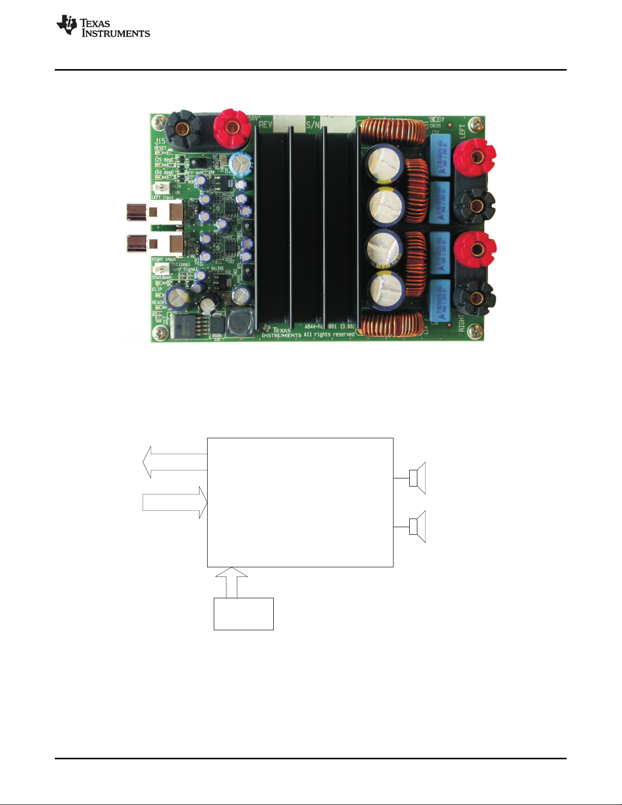
2 x AnalogInput
TAS5611/13PHD2EVM
MODULE
PowerSupply
2 Channel
SpeakerOutput
+12 VFanOut
Control
www.ti.com
This document covers EVM specifications, audio performance and power efficiency measurements
graphs, and design documentation that includes schematics, parts list, layout, and mechanical design.
Overview
1.1 TAS5611/13PHD2EVM Features
• Stereo PurePath™ Premier Pro evaluation module.
• Self-contained protection system (short circuit and thermal).
• Standard 1VRMS single ended line input or differential input.
• Double-sided, plated-through PCB layout.
Figure 1. Integrated PurePath™ Digital Amplifier System
1.2 PCB Key Map
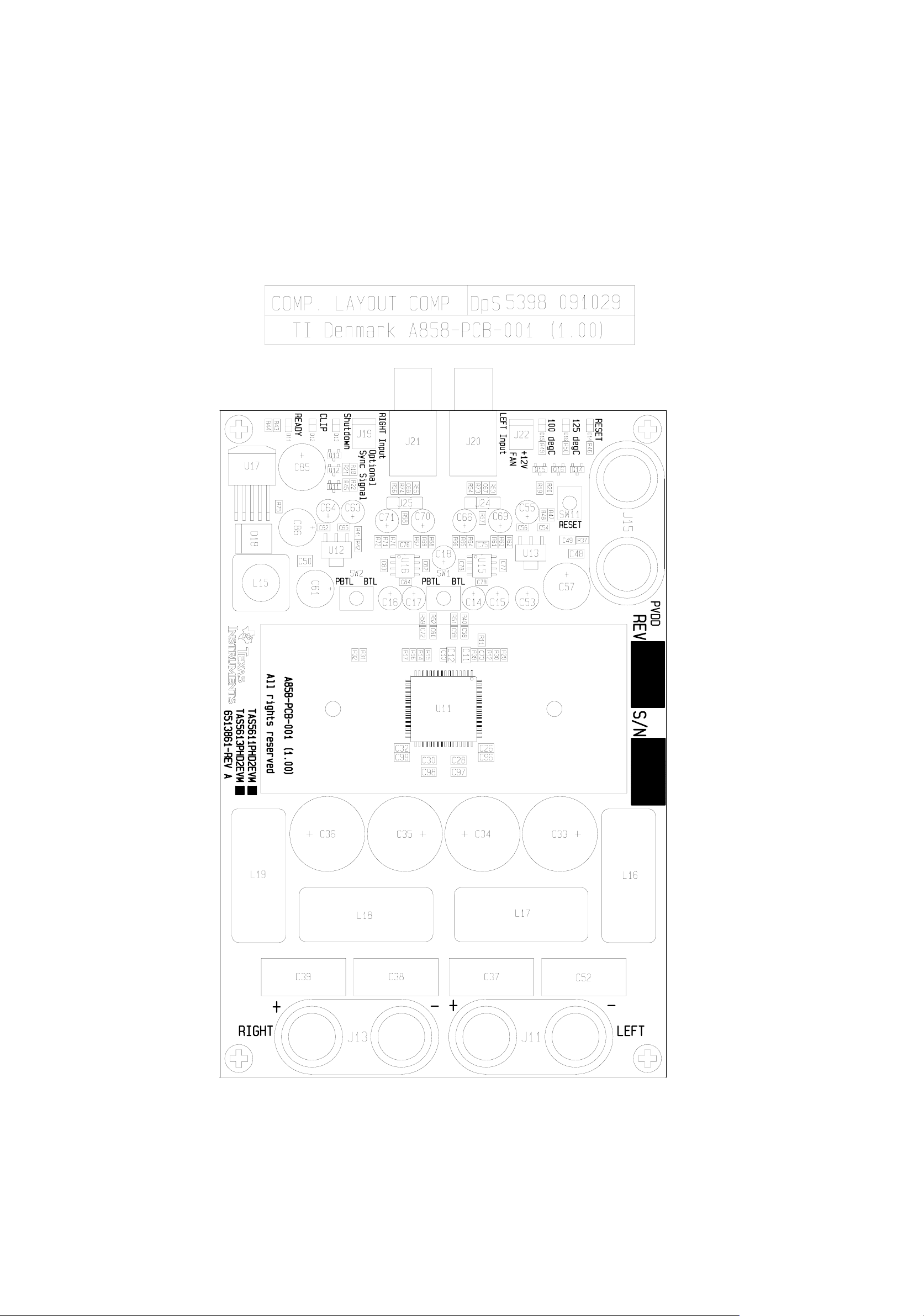
Physical structure for the TAS5611/13PHD2EVM is illustrated in Figure 2.
SLOU286–December 2009 TAS5611/13PHD2EVM
Submit Documentation Feedback
Copyright © 2009, Texas Instruments Incorporated
3
Page 4
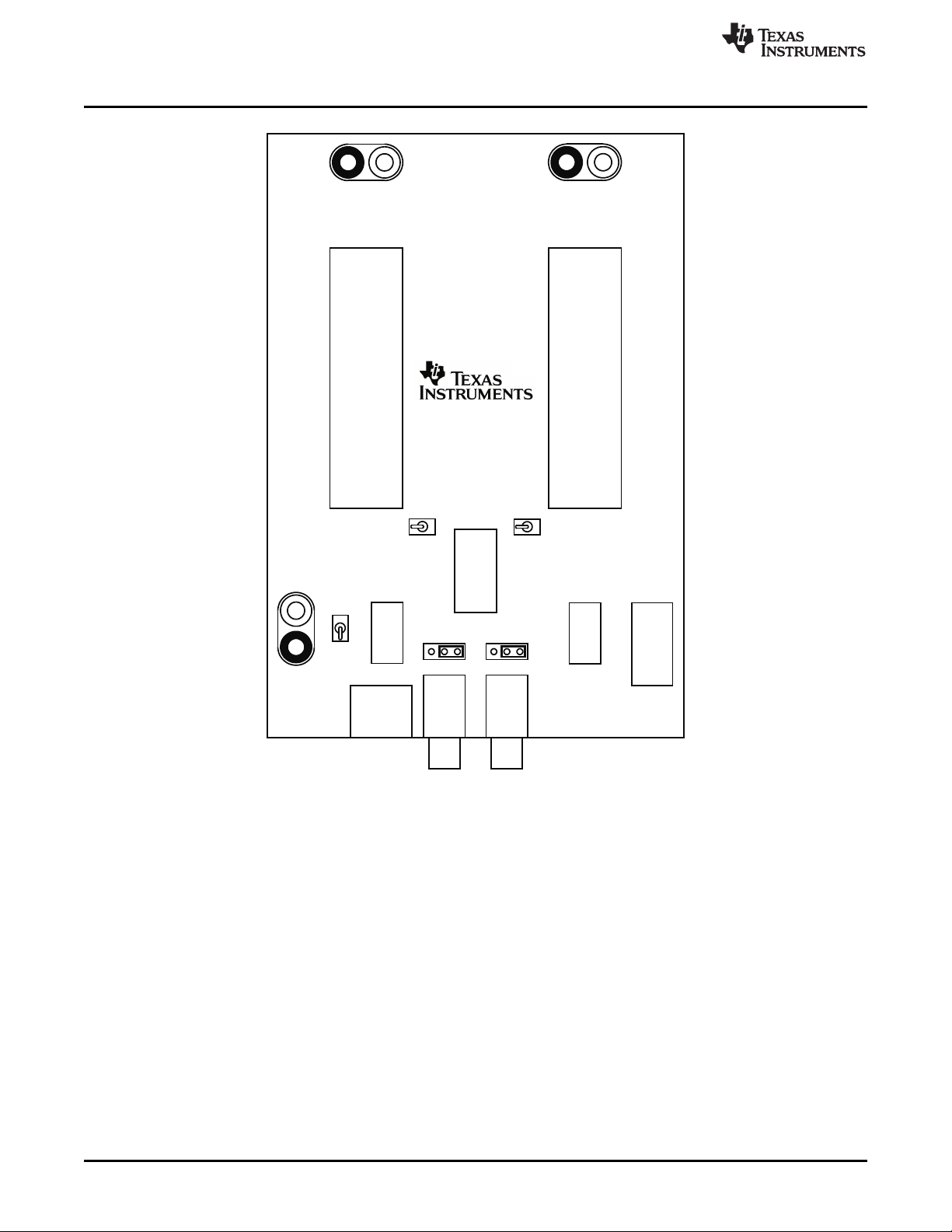
+12 V
Regulator
SE LEFT
INPUT
(J20)
OUTPUT STAGE
CHANNEL LEFT
OUTPUT STAGE
CHANNEL RIGHT
SE RIGHT
INPUT
(J21)
RESET
(SW11)
SE TO DIFF
CONVERTERS
(U15 & U16)
PVDD
(J15)
LEFT
SPEAKER
OUTPUT
(J11)
RIGHT
SPEAKER
OUTPUT
(J13)
+12 V FAN
Regulator
DIFFINPUT
(J24)
DIFFINPUT
(J25)
+12VFAN
OUT
CONTROL
(J22)
JUMPER1 JUMPER2
+15 V
Switcher
(SW1) (SW2)
PBTLPBTLBTL BTL
Overview
www.ti.com
Figure 2. Physical Structure for the TAS53630PHDEVM (Approximate Layout)
4
TAS5611/13PHD2EVM SLOU286–December 2009
Submit Documentation Feedback
Copyright © 2009, Texas Instruments Incorporated
Page 5

www.ti.com
2 Quick Setup Guide
This chapter describes the TAS5611/13PHD2EVM board in regards to power supply and system
interfaces. The chapter provides information regarding handling and unpacking, absolute operating
conditions, and a description of the factory default switch and jumper configuration.
This section provides a step–by–step guide to configuring the TAS5611/13PHD2EVM for device
evaluation
2.1 Electrostatic Discharge Warning
Many of the components on the TAS5611/13PHD2EVM are susceptible to damage by electrostatic
discharge (ESD). Customers are advised to observe proper ESD handling precautions when unpacking
and handling the EVM, including the use of a grounded wrist strap at an approved ESD workstation.
Failure to observe ESD handling procedures may result in damage to EVM
components.
2.2 Unpacking the EVM
On opening the TAS5611/13PHD2EVM package, ensure that the following items are included:
• 1 pc. TAS5611/13PHD2EVM board using one TAS5611PHD or one TAS5613PHD.
If any of the items are missing, contact the Texas Instruments Product Information Center nearest you to
inquire about a replacement.
Quick Setup Guide
CAUTION
2.3 Power Supply Setup
To power up the EVM, one power supply are needed. An onboard switched voltage regulator is supplying
system power, logic and gate-drive. Power supply is connected to the EVM using connector J15.
NOTE: While powering up set switch SW11 to the RESET position.
Description Voltage Limitations Current Requirement Cable
TAS5613 Output stage power 18V - 36V 16 A J15 (marked PVDD)
supply
TAS5611 Output stage power 16V - 32.5V 16A J15 (marked PVDD)
supply
Applying voltages above the limitations given in Table 2 may cause permanent
damage to your hardware
NOTE: The length of power supply cable must be minimized. Increasing length of PSU cable is
equal to increasing the distortion for the amplifier at high output levels and low frequencies.
Table 2. Recommended Supply Voltages
CAUTION
2.4 Applying Input Signal
It is possible to apply either a single ended input signal to J20 and J21 or a differential input signal to J24
and J25.
SLOU286–December 2009 TAS5611/13PHD2EVM
Submit Documentation Feedback
Copyright © 2009, Texas Instruments Incorporated
5
Page 6
+12 V
Regulator
SE LEFT
INPUT
(J20)
SE RIGHT
INPUT
(J21)
RESET
(SW11)
PVDD
(J15)
+12 V FAN
Regulator
DIFFINPUT
(J24)
DIFFINPUT
(J25)
+12VFAN
OUT
CONTROL
(J22)
JUMPER1 JUMPER2
Quick Setup Guide
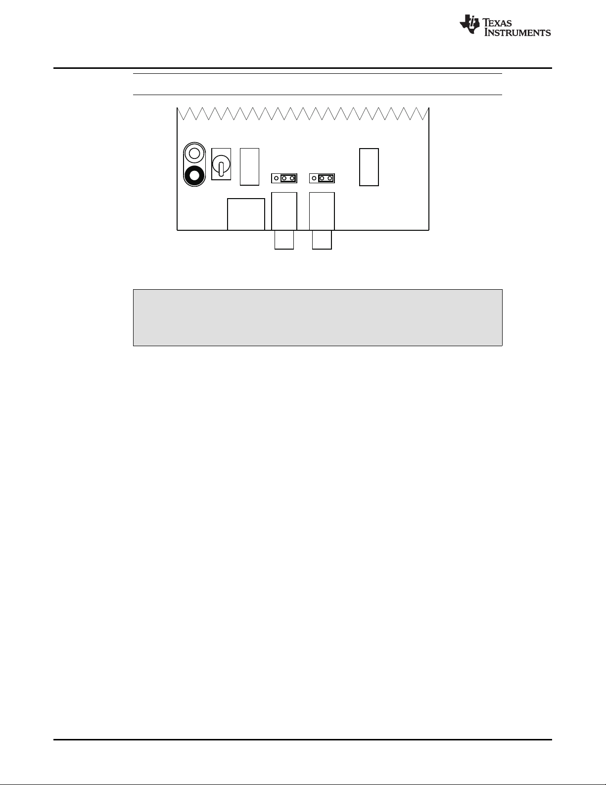
NOTE: If a single ended input signal is applied please insert jumpers in the header J24 and J25.
2.5 Speaker Connection
Both positive and negative speaker outputs are floating and may not be
connected to ground (e.g., through an oscilloscope).
www.ti.com
CAUTION
2.6 Output configuration BTL and PBTL
When changing mode e.g. from BTL to PBTL make sure that RESET switch (SW11) is activated before
changing the state of mode switches SW1 and SW2. Switch SW1 and SW2 has to be synchronized in
state BTL or PBTL.
Input signal to RCA connector J20 when operating PBTL mode. J21 is disabled.
In PBTL mode, the load has to be connected according to Figure 3:
6
TAS5611/13PHD2EVM SLOU286–December 2009
Submit Documentation Feedback
Copyright © 2009, Texas Instruments Incorporated
Page 7
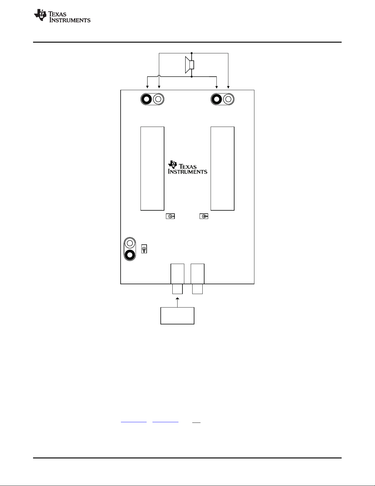
SE LEFT
INPUT
(J20)
OUTPUT STAGE
CHANNEL LEFT
OUTPUT STAGE
CHANNEL RIGHT
SE RIGHT
INPUT
(J21)
RESET
(SW11)
PVDD
(J15)
LEFT BTL
SPEAKER
OUTPUT
(J11)
RIGHT BTL
SPEAKER
OUTPUT
(J13)
(SW1) (SW2)
PBTLPBTLBTL BTL
PBTL
PBTL Mode.:
Input
Signal
www.ti.com
Protection
Figure 3. Figure 3. PBTL Mode Configuration
3 Protection
This section describes the short-circuit protection and fault-reporting circuitry of the TAS5611 and
TAS5613 devices.
3.1 Short-Circuit Protection and Fault-Reporting Circuitry
The TAS5611 and TAS5613 is self-protecting devices that provides fault reporting (including
high-temperature protection and short-circuit protection). TAS5611 and TAS5613 is configured in
back-end auto-recovery mode, and therefore; resets automatically after all errors (M1, M2, and M3 is set
low); see the data sheet (SLAS681) (SLAS676) for further explanation. This mean that the device restart
itself after an error occasion and report through the SD error signal.
SLOU286–December 2009 TAS5611/13PHD2EVM
Submit Documentation Feedback
Copyright © 2009, Texas Instruments Incorporated
7
Page 8
Related Documentation from Texas Instruments
3.2 Fault Reporting
The OTW and SD outputs from TAS5611/13 indicate fault conditions. See the
TAS5611PHD/TAS5613PHD data manual for a description of these pins.
Table 3. TAS5611/13 Warning/Error Signal Decoding
SD OTW1 OTW2 Device Condition
0 0 0 High-temperature error and/or high-current error
0 0 1 Undervoltage lockout or high current error. 100°C
temperature warning.
0 1 1 Undervoltage lockout or high-current error
1 0 0 125°C temperature warning
1 0 1 100°C temperature warning
1 1 1 Normal operation, no errors/warnings
The shutdown signals together with the temperature warning signal give chip-state information as
described in the Table 3. device fault-reporting outputs are open-drain outputs.
4 Related Documentation from Texas Instruments
Table 4 contains a list of data manuals that have detailed descriptions of the integrated circuits used in the
design of the TAS5611/13PHD2EVM. The data manuals can be obtained at the URL http://www.ti.com.
Table 4. Related Documentation from
Texas Instruments
www.ti.com
4.1 Additional Documentation
1. System Design Considerations for True Digital Audio Power Amplifiers application report (SLAA117)
2. Digital Audio Measurements application report (SLAA114)
3. PSRR for PurePath Digital™ Audio Amplifiers application report (SLEA049)
4. Power Rating in Audio Amplifiers application report (SLEA047)
5. PurePath Digital™ AM Interference Avoidance application report (SLEA040)
6. Click and Pop Measurements Technique application report (SLEA044)
7. Power Supply Recommendations for DVD-Receivers application report (SLEA027)
8. Implementation of Power Supply Volume Control application report (SLEA038)
Appendix A Design Documents
This appendix comprises design documents pertaining to the TAS5611/13PHD2EVM evaluation module.
The documents are presented in the following order.
• Schematic (4 pages)
• Parts List (1 pages)
• PCB Specification (1 page)
• PCB Layers (6 pages)
• Heat-Sink Drawing (1 page)
• Inductor (1 page)
Part Number Literature Number
TAS5611 SLAS681
TAS5613 SLAS676
OPA1632D SBOS286
LM317M SLVS297
TL2575HV-15I SLVS638
8
Design Documents SLOU286–December 2009
Copyright © 2009, Texas Instruments Incorporated
Submit Documentation Feedback
Page 9

Evaluation Board/Kit Important Notice
Texas Instruments (TI) provides the enclosed product(s) under the following conditions:
This evaluation board/kit is intended for use for ENGINEERING DEVELOPMENT, DEMONSTRATION, OR EVALUATION
PURPOSES ONLY and is not considered by TI to be a finished end-product fit for general consumer use. Persons handling the
product(s) must have electronics training and observe good engineering practice standards. As such, the goods being provided are
not intended to be complete in terms of required design-, marketing-, and/or manufacturing-related protective considerations,
including product safety and environmental measures typically found in end products that incorporate such semiconductor
components or circuit boards. This evaluation board/kit does not fall within the scope of the European Union directives regarding
electromagnetic compatibility, restricted substances (RoHS), recycling (WEEE), FCC, CE or UL, and therefore may not meet the
technical requirements of these directives or other related directives.
Should this evaluation board/kit not meet the specifications indicated in the User’s Guide, the board/kit may be returned within 30
days from the date of delivery for a full refund. THE FOREGOING WARRANTY IS THE EXCLUSIVE WARRANTY MADE BY
SELLER TO BUYER AND IS IN LIEU OF ALL OTHER WARRANTIES, EXPRESSED, IMPLIED, OR STATUTORY, INCLUDING
ANY WARRANTY OF MERCHANTABILITY OR FITNESS FOR ANY PARTICULAR PURPOSE.
The user assumes all responsibility and liability for proper and safe handling of the goods. Further, the user indemnifies TI from all
claims arising from the handling or use of the goods. Due to the open construction of the product, it is the user’s responsibility to
take any and all appropriate precautions with regard to electrostatic discharge.
EXCEPT TO THE EXTENT OF THE INDEMNITY SET FORTH ABOVE, NEITHER PARTY SHALL BE LIABLE TO THE OTHER
FOR ANY INDIRECT, SPECIAL, INCIDENTAL, OR CONSEQUENTIAL DAMAGES.
TI currently deals with a variety of customers for products, and therefore our arrangement with the user is not exclusive.
TI assumes no liability for applications assistance, customer product design, software performance, or infringement of
patents or services described herein.
Please read the User’s Guide and, specifically, the Warnings and Restrictions notice in the User’s Guide prior to handling the
product. This notice contains important safety information about temperatures and voltages. For additional information on TI’s
environmental and/or safety programs, please contact the TI application engineer or visit www.ti.com/esh.
No license is granted under any patent right or other intellectual property right of TI covering or relating to any machine, process, or
combination in which such TI products or services might be or are used.
FCC Warning
This evaluation board/kit is intended for use for ENGINEERING DEVELOPMENT, DEMONSTRATION, OR EVALUATION
PURPOSES ONLY and is not considered by TI to be a finished end-product fit for general consumer use. It generates, uses, and
can radiate radio frequency energy and has not been tested for compliance with the limits of computing devices pursuant to part 15
of FCC rules, which are designed to provide reasonable protection against radio frequency interference. Operation of this
equipment in other environments may cause interference with radio communications, in which case the user at his own expense
will be required to take whatever measures may be required to correct this interference.
EVM Warnings and Restrictions
It is important to operate this EVM within the input voltage range of 0 V to 32.5 V for the TAS5611; 0 V to 36 V for the TAS5613
and the output voltage range of 0 V to 32.5 V for the TAS5611; 0 V to 36 V for the TAS5613.
Exceeding the specified input range may cause unexpected operation and/or irreversible damage to the EVM. If there are
questions concerning the input range, please contact a TI field representative prior to connecting the input power.
Applying loads outside of the specified output range may result in unintended operation and/or possible permanent damage to the
EVM. Please consult the EVM User's Guide prior to connecting any load to the EVM output. If there is uncertainty as to the load
specification, please contact a TI field representative.
During normal operation, some circuit components may have case temperatures greater than 90°C. The EVM is designed to
operate properly with certain components above 125°C as long as the input and output ranges are maintained. These components
include but are not limited to linear regulators, switching transistors, pass transistors, and current sense resistors. These types of
devices can be identified using the EVM schematic located in the EVM User's Guide. When placing measurement probes near
these devices during operation, please be aware that these devices may be very warm to the touch.
Mailing Address: Texas Instruments, Post Office Box 655303, Dallas, Texas 75265
Copyright © 2009, Texas Instruments Incorporated
Page 10
5
TI
D D
Design Name:
Type: Mass Market EVM
File Name: A858-SCH-001.DSN
Version:
Date:
Design Engineer:
Audio Configuration:
C C
Interfaces:
Setup:
Performance: 2 x 150 W / 4 Ohm (BTL) 10% THD+N
B B
Page
1/4: Front Page and Schematic Disclaimer
2/4: TAS5613 Amplifier
3/4: Input Stage
4/4: Mechanics
TAS5613PHD2EVM
1.00
24.Oct. 2009
Jonas Holm
PurePath Premire Pro Digital Amplifier Design
1 x TAS5613PHD
J20-J21: Single Ended Analog Audio Input
J11, J13: Banana Bindingposts For Speakers
J15: Banana Bindingpost For H-Bridge Supply
4 Ohm (BTL) Speaker Loads
+36 V H-Bridge Supply Voltage
> 102 dB Dynamic Range
4
3
NOTE1
NOTE1
The preliminary schematic information and materials ("Materials") provided here are provided by Texas Instruments
The preliminary schematic information and materials ("Materials") provided here are provided by Texas Instruments
Incorporated ("TI") as a service to its customers and/or suppliers, and may be used for informational purposes only, and
Incorporated ("TI") as a service to its customers and/or suppliers, and may be used for informational purposes only, and
only subject to the following terms. By downloading or viewing these Materials, you are signifying your assent to these
only subject to the following terms. By downloading or viewing these Materials, you are signifying your assent to these
terms.
terms.
1.) These preliminary evaluation schematics are intended for use for PRELIMINARY ENGINEERING
1.) These preliminary evaluation schematics are intended for use for PRELIMINARY ENGINEERING
DEVELOPMENT AND EVALUATION PURPOSES ONLY and are not considered by Texas Instruments to be fit as a
DEVELOPMENT AND EVALUATION PURPOSES ONLY and are not considered by Texas Instruments to be fit as a
basis for establishing production products or systems. This information may be incomplete in several respects, including
basis for establishing production products or systems. This information may be incomplete in several respects, including
but not limited to information relating to required design, marketing, and/or manufacturing-related protective
but not limited to information relating to required design, marketing, and/or manufacturing-related protective
considerations and product safety measures typically found in the end-product incorporating the
considerations and product safety measures typically found in the end-product incorporating the
goods.
goods.
2.) Accordingly, neither TI nor its suppliers warrant the accuracy or completeness of the information, text,
2.) Accordingly, neither TI nor its suppliers warrant the accuracy or completeness of the information, text,
graphics, links or other items contained within the Materials. TI may make changes to the Materials, or to the products
graphics, links or other items contained within the Materials. TI may make changes to the Materials, or to the products
described therein, at any time without notice. TI makes no commitment to update the Materials.
described therein, at any time without notice. TI makes no commitment to update the Materials.
3.) TI assumes no liability for applications assistance, customer product design, software performance, or services
3.) TI assumes no liability for applications assistance, customer product design, software performance, or services
that may be described or referenced in the Materials. The user assumes all responsibility and liability for proper and safe
that may be described or referenced in the Materials. The user assumes all responsibility and liability for proper and safe
design and handling of goods. Accordingly, the user indemnifies TI from all claims arising from its use of the Materials.
design and handling of goods. Accordingly, the user indemnifies TI from all claims arising from its use of the Materials.
4.) TI currently deals with various customers for products, and therefore our arrangement with the user will not be
4.) TI currently deals with various customers for products, and therefore our arrangement with the user will not be
exclusive. TI makes no representations regarding the commercial availability of non-TI components that may be
exclusive. TI makes no representations regarding the commercial availability of non-TI components that may be
referenced in the Materials.
referenced in the Materials.
5.) No license is granted under any patent right or other intellectual property right of TI covering or relating to any
5.) No license is granted under any patent right or other intellectual property right of TI covering or relating to any
combination, machine, or process in which such TI products or services might be or are used. Except as expressly
combination, machine, or process in which such TI products or services might be or are used. Except as expressly
provided herein, TI and its suppliers do not grant any express or implied right to you under any patents, copyrights,
provided herein, TI and its suppliers do not grant any express or implied right to you under any patents, copyrights,
trademarks, or trade secret information.
trademarks, or trade secret information.
6.) Performance tests and ratings, to the extent referenced in the Materials, are measured using specific computer
6.) Performance tests and ratings, to the extent referenced in the Materials, are measured using specific computer
systems and/or components and reflect the approximate performance of TI products as measured by those tests. Any
systems and/or components and reflect the approximate performance of TI products as measured by those tests. Any
difference in system hardware or software design or configuration may affect actual performance. Buyers should consult
difference in system hardware or software design or configuration may affect actual performance. Buyers should consult
other sources of information to evaluate the performance of systems or components they are considering purchasing.
other sources of information to evaluate the performance of systems or components they are considering purchasing.
7.) Resale of TI's products or services with statements different from or beyond the parameters stated by TI for that
7.) Resale of TI's products or services with statements different from or beyond the parameters stated by TI for that
product or service in official TI data books or data sheets voids all express and any implied warranties for the associated
product or service in official TI data books or data sheets voids all express and any implied warranties for the associated
TI product or service, and is an unfair and deceptive business practice, and TI is not responsible for any such use.
TI product or service, and is an unfair and deceptive business practice, and TI is not responsible for any such use.
8.) The Materials are copyrighted and any unauthorized use may violate copyright, trademark, and other laws. You
8.) The Materials are copyrighted and any unauthorized use may violate copyright, trademark, and other laws. You
may only download one copy for your internal use only, unless you are specifically licensed to do otherwise by TI in
may only download one copy for your internal use only, unless you are specifically licensed to do otherwise by TI in
writing. This is a license, not a transfer of title, and is subject to the following restrictions: You may not: (a) modify the
writing. This is a license, not a transfer of title, and is subject to the following restrictions: You may not: (a) modify the
Materials (including any associated warranties, conditions, limitations or notices) or use them for any commercial
Materials (including any associated warranties, conditions, limitations or notices) or use them for any commercial
purpose, or any public display, performance, sale or rental; (b) decompile, reverse engineer, or disassemble software
purpose, or any public display, performance, sale or rental; (b) decompile, reverse engineer, or disassemble software
Materials except and only to the extent permitted by applicable law; (c) remove any copyright or other proprietary notices
Materials except and only to the extent permitted by applicable law; (c) remove any copyright or other proprietary notices
from the Materials; (d) transfer the Materials to another person. You agree to prevent any unauthorized copying of the
from the Materials; (d) transfer the Materials to another person. You agree to prevent any unauthorized copying of the
Materials. TI may terminate this license at any time if you are in breach of the terms of this Agreement. Upon termination,
Materials. TI may terminate this license at any time if you are in breach of the terms of this Agreement. Upon termination,
you will immediately destroy the Materials.
you will immediately destroy the Materials.
9.) THE MATERIALS ARE PROVIDED "AS IS" WITHOUT ANY EXPRESS OR IMPLIED
9.) THE MATERIALS ARE PROVIDED "AS IS" WITHOUT ANY EXPRESS OR IMPLIED
WARRANTY OF ANY KIND INCLUDING WARRANTIES OF MERCHANTABILITY,
WARRANTY OF ANY KIND INCLUDING WARRANTIES OF MERCHANTABILITY,
NONINFRINGEMENT OF INTELLECTUAL PROPERTY, OR FITNESS FOR ANY PARTICULAR
NONINFRINGEMENT OF INTELLECTUAL PROPERTY, OR FITNESS FOR ANY PARTICULAR
PURPOSE. IN NO EVENT SHALL TI OR ITS SUPPLIERS BE LIABLE FOR ANY DAMAGES
PURPOSE. IN NO EVENT SHALL TI OR ITS SUPPLIERS BE LIABLE FOR ANY DAMAGES
WHATSOEVER (INCLUDING, WITHOUT LIMITATION, DAMAGES FOR LOSS OF PROFITS, BUSINESS
WHATSOEVER (INCLUDING, WITHOUT LIMITATION, DAMAGES FOR LOSS OF PROFITS, BUSINESS
INTERRUPTION, LOSS OF INFORMATION) ARISING OUT OF THE USE OF OR INABILITY TO USE
INTERRUPTION, LOSS OF INFORMATION) ARISING OUT OF THE USE OF OR INABILITY TO USE
THE MATERIALS, EVEN IF TI HAS BEEN ADVISED OF THE POSSIBILITY OF SUCH DAMAGES.
THE MATERIALS, EVEN IF TI HAS BEEN ADVISED OF THE POSSIBILITY OF SUCH DAMAGES.
2
SCHEMATIC DISCLAIMER
SCHEMATIC DISCLAIMER
1
Not Used
Not Used
A A
/ TAS5613 Parts list 1.00
/ TAS5613 Parts list 1.00
Copyright 2008 Texas Instruments, Inc - All rights reserved - The TI and PurePath Digital logos are trademarks of Texas Instruments.
5
4
3
/ TAS5613 Parts list 1.00
TI
TI
TI
Project:
TAS5613PHD2EVM
Project:
TAS5613PHD2EVM
Project:
TAS5613PHD2EVM
Page Title:
Disclaimer
Page Title:
Disclaimer
Page Title:
Disclaimer
File Name:
File Name:
File Name:
A858-SCH-001.DSN
A858-SCH-001.DSN
A858-SCH-001.DSN
Date:
Date:
Date:
Monday, October 26, 2009 1 4
Monday, October 26, 2009 1 4
2
Monday, October 26, 2009 1 4
AUDIO/IMAGING GROUP
AUDIO/IMAGING GROUP
AUDIO/IMAGING GROUP
Home Audio Amplifiers
Home Audio Amplifiers
Home Audio Amplifiers
ALL RIGHTS RESERVED
ALL RIGHTS RESERVED
ALL RIGHTS RESERVED
TEXAS INSTRUMENTS INCORPORATED
TEXAS INSTRUMENTS INCORPORATED
TEXAS INSTRUMENTS INCORPORATED
Rev:
Rev:
Rev:
1.00
1.00
1.00
Size:
A3
Size:
A3
Size:
A3
Page: of
Page: of
Page: of
1
Engineer:
Engineer:
Engineer:
Jonas L. Holm
Jonas L. Holm
Jonas L. Holm
Page 11

5
D D
R11
R11
/RESET
C14
C14
1 2
L_IN_P
L_IN_N
R_IN_P
R_IN_N
C C
B B
10uF
10uF
C15
C15
1 2
10uF
10uF
C16
C16
1 2
10uF
10uF
C17
C17
1 2
10uF
10uF
Optional
Sync signal
12
C73
C73
100R
100R
100pF
100pF
2 1
R40
R40
12
C58
C58
100R
100R
100pF
100pF
2 1
R51
R51
12
C59
C59
100R
100R
100pF
100pF
VREG
2 1
R52
R52
12
C60
C60
100R
100R
100pF
100pF
2 1
R59
R59
12
C72
C72
100R
100R
100pF
100pF
2 1
J19
J19
1
2
Header
Header
/SD
/OTW1
/OTW2
/CLIP
READY
1
3
6
4
/OTW1
/OTW2
/CLIP
READY
4
+12V
C18
C18
10uF
10uF
GND
C20
C20
2 1
GND
VREG
12
R39
R39
47k
47k
SW1
SW1
GND
2
5
Switch
Switch
GND
R16
R16
OSC_IOP
12
100R
100R
R17
R17
OSC_IOM
12
100R
100R
/SD
VREG
VREG
GND
GND
GND
GND
R14
R14
Not Used
Not Used
10k
10k
R19
R19
100R
100R
C13
C13
100nF
100nF
R15
R15
R18
R18
100R
100R
12
12
330pF
330pF
R12
R12
30.0k
30.0k
C11
C11
2 1
4.7nF
4.7nF
C12
C12
2 1
1nF
1nF
VREG
21
12
12
R20
R20
100R
100R
1
3
6
4
12
SW2
SW2
Switch
Switch
1
12
2
3
4
5
6
7
8
GNDGND
9
10
11
12
13
14
15
16
R21
R21
100R
100R
2
5
R29
R29
1 2
3.3R
3.3R
R30
R30
12
GND
OC_ADJ
/RESET
C_STARTUP
INPUT_A
INPUT_B
VI_CM
GND
AGND
VREG
INPUT_C
INPUT_D
FREQ_ADJ
OSC_IO+
OSC_IO-
/SD
/OTW1
12
R22
R22
100R
100R
1 2
3.3R
3.3R
C19
C19
100nF
100nF
2 1
12
C21
C21
100nF
100nF
2 1
GND
64
63
59
NC62NC61NC60NC
VDD
PSU_REF
/OTW217/CLIP18READY19M120M221M322GND23GND24GVDD_C25GVDD_D26BST_D27OUT_D28OUT_D29PVDD_D30PVDD_D31GND_D
C22
C22
100nF
100nF
GND58GND
3.3R
3.3R
1 2
R31
R31
2 1
57
GVDD_B56GVDD_A
U11
U11
PTAS5613PHD
PTAS5613PHD
GND
21
100nF
100nF
C23
C23
GND
3
C28, C30, C97 and C98: It is important to choose either a
1206 or 1210 footprint for these decoupling capacitors to
have the posibility to take the audio output trace directly
under the capacitor in layout!
C25
C25
33nF
33nF
21
C26
C26
1uF
1uF
50V
50V
0805
0805
50
OUT_A53OUT_A
R32
R32
52
+12V+12V
12
21
PVDD_A51PVDD_A
49
GND_A
32
C32
C32
1uF
1uF
50V
50V
0805
0805
55
54
BST_A
33nF
33nF
C31
C31
3.3R
3.3R
21
100nF
100nF
C24
C24
GND
0805
0805
2 1
GND_A
GND_B
GND_B
OUT_B
OUT_B
PVDD_B
PVDD_B
BST_B
BST_C
PVDD_C
PVDD_C
OUT_C
OUT_C
GND_C
GND_C
GND_D
2 1
PVDD
C96
C96
12
1uF
1uF
50V
50V
C33
C33
1000uF
1000uF
2 1
50V
50V
GND
48
47
46
GND
45
C28
C28
44
1uF
1uF
50V
50V
43
1206
1206
2 1
42
41
40
39
C30
C30
38
1uF
1uF
50V
50V
37
1206
1206
2 1
36
35
34
GND
33
C99
C99
1uF
1uF
C36
C36
50V
50V
1000uF
1000uF
0805
0805
PVDD
50V
50V
2 1
1 2
21
C27
C27
C97
C97
33nF
33nF
1uF
1uF
50V
50V
1206
1206
2 1
21
C98
C98
C29
C29
1uF
1uF
33nF
33nF
50V
50V
1206
1206
2 1
PVDD
12
C35
C35
1000uF
1000uF
50V
50V
GND
OUT_A OUT_LM
OUT_B
PVDD
12
GND
OUT_C
OUT_D
1
3
L11
L11
Not Used
Not Used
DAEPWG-M251
DAEPWG-M251
C34
C34
1000uF
1000uF
50V
50V
1
3
L12
L12
Not Used
Not Used
DAEPWG-M251
DAEPWG-M251
2
2
C52
C52
C40
C40
680nF
680nF
1nF
1nF
2 1
GND
C37
C37
C41
C41
680nF
680nF
1nF
1nF
2 1
OUT_LP
4
PVDD
12
C57
C57
47uF
47uF
63V
63V
GND
OUT_RM
2
C42
C42
C38
C38
1nF
1nF
680nF
680nF
2 1
GND
C39
C39
C43
C43
680nF
680nF
1nF
1nF
2 1
OUT_RP
4
12
R33
R33
3.3R
3.3R
C44
C44
2 1
10nF
10nF
2 1
GND
C45
C45
10nF
10nF
2 1
12
R34
R34
3.3R
3.3R
2 1
12
R37
R37
3.3R
3.3R
C48
C48
1uF
1uF
50V
50V
C49
C49
2 1
10nF
10nF
2 1
GND
GND
GND
12
R35
R35
3.3R
3.3R
C46
C46
10nF
10nF
2 1
2 1
GND
C47
C47
10nF
10nF
2 1
12
R36
R36
3.3R
3.3R
2 1
J11J11
-
LEFT
4 OHM BTL
1
SPEAKER
2
OUTPUT
+
High Power
supply
J15J15
1
PVDD
2
GND
J13J13
-
RIGHT
1
4 OHM BTL
2
SPEAKER
OUTPUT
+
1
3 OHM LOAD OPERATION:
1) Mount Schottky diodes (D24, D25, D26 and D27)
2) Change ROC = 22kOhm (R12)
OUT_DOUT_COUT_BOUT_A
D27
D27
D26
D26
D25
D25
D24
D24
Not Used
Not Used
Not Used
Not Used
GND GND GND GND
A A
5
4
3
Not Used
Not Used
Not Used
Not Used
OUTPUT INDUCTOR STUFFING OPTION:
L16
L16
10uH
10uH
OUT_A OUT_LM
1 2
L17
L17
10uH
10uH
OUT_B OUT_LP
1 2
L18
L18
10uH
10uH
OUT_C OUT_RM
1 2
L19
L19
10uH
10uH
OUT_D OUT_RP
1 2
2
OUT_A OUT_LM
1
2
OUT_B OUT_LP
3
4
L20
L20
Not Used
Not Used
/ TAS5613 Parts list 1.00
/ TAS5613 Parts list 1.00
/ TAS5613 Parts list 1.00
TI
TI
TI
TAS5613PHD2EVM
TAS5613PHD2EVM
TAS5613PHD2EVM
Project:
Project:
Project:
Page Title:
Main Schematic
Page Title:
Main Schematic
Page Title:
Main Schematic
A858-SCH-001.DSN
A858-SCH-001.DSN
A858-SCH-001.DSN
File Name:
File Name:
File Name:
Thursday, October 29, 2009 2 4
Thursday, October 29, 2009 2 4
Thursday, October 29, 2009 2 4
Date:
Date:
Date:
OUT_C
1
OUT_D
3
L22
L22
Not Used
Not Used
TEXAS INSTRUMENTS INCORPORATED
TEXAS INSTRUMENTS INCORPORATED
TEXAS INSTRUMENTS INCORPORATED
1
OUT_RM
2
OUT_RP
4
AUDIO/IMAGING GROUP
AUDIO/IMAGING GROUP
AUDIO/IMAGING GROUP
Home Audio Amplifiers
Home Audio Amplifiers
Home Audio Amplifiers
ALL RIGHTS RESERVED
ALL RIGHTS RESERVED
ALL RIGHTS RESERVED
Rev:
Rev:
Rev:
Size:
Size:
Size:
Jonas L. Holm
Jonas L. Holm
Jonas L. Holm
Engineer:
Engineer:
Engineer:
Page: of
Page: of
Page: of
1.00
1.00
1.00
A2
A2
A2
Page 12
5
4
3
2
1
+12V
SW11
U12
2 1
C62
C62
100nF
100nF
U12
LM317
LM317
IN3OUT
R41
R41
4.7k
4.7k
GND GND
R43
1 2
READY
32
GND
R43
4.7k
4.7k
D11
D11
Green
Green
10uF
10uF
C64
C64
12
GND GND
+12V
C65
C65
100nF
100nF
2 1
2
4
OUT
ADJ
1
12
R42
R42
560R
560R
12
12
C63
C63
10uF
10uF
Q11
Q11
2N7002
2N7002
1
R44
R44
4.7k
4.7k
1 2
D12
D12
Yellow
Yellow
32
GND GND
Q12
Q12
2N7002
2N7002
1
CLIP
R45
R45
4.7k
4.7k
1 2
D13
D13
Red
Red
Q13
Q13
2N7002
2N7002
1
Shutdown
/SD
/CLIP
READY
32
+15V
D D
C61
C61
470uF
470uF
12
GND GND
SW11
2
5
Switch
Switch
R46
R46
4.7k
4.7k
1 2
D14
D14
Red
Red
RESET
GND GND
+12V
1
3
6
4
GND
/RESET
32
Q14
Q14
2N7002
2N7002
1
ON/OFF ControlSTATUS MONITOR12V lin regulator
C C
C69
LEFT Input
Phono socket
Phono socket
J20
J20
B B
Jumper J24 & J25 pin 1-2
4
3
2
1
Shunt Header
Shunt Header
3
R570RR57
2
J24
J24
0R
1
12
GND
R530RR53
0R
R540RR54
0R
12
C67
C67
1nF
1nF
2 1
12
C69
10uF
10uF
12
R73
R73
100k
100k
C66
C66
10uF
10uF
12
12
R61
R61
2.2k
2.2k
1 2
1 2
R64
R64
2.2k
2.2k
1 2
C75
C75
470pF
470pF
2 1
1 2
R63
R63
2.2k
2.2k
R65
R65
2.2k
2.2k
U15
U15
OPA1632
OPA1632
For single inded input
8
2
1
C77 150pFC77 150pF
1 2
R62 10.0kR62 10.0k
+12V
V_OCM
V_OCM
EN
EN
R66 10.0kR66 10.0k
1 2
C78 150pFC78 150pF
21
C79
C79
21
3
100nF
100nF
GND
V+
V+
5
4
V-
V-
67
GND
21
L_IN_N
L_IN_P
+15V
12
C55
C55
10uF
10uF
GND GND
100 degC
Chip temp
125 degC
Chip temp
PVDD
12
C85
C85
330uF
330uF
63V
63V
+15V Switcher
2 1
C56
C56
100nF
100nF
U17
U17
TL2575HV-15I
TL2575HV-15I
1
U13
U13
LM317
LM317
IN3OUT
VIN
GND
R49
R49
1.00k
1.00k
Yellow
Yellow
R50
R50
820R
820R
Red
Red
GND
3
D15
D15
D16
D16
2
4
OUT
ADJ
1
1 2
1 2
6
ON/OFF5GND-PAD
OUTPUT
R75
R75
10R
10R
GND
FB
1 2
1 2
GND
32
4
2
12
R47
R47
560R
560R
R48
R48
1.2k
1.2k
32
Q16
Q16
2N7002
2N7002
1
12
C53
C53
10uF
10uF
GND GND
Q15
Q15
2N7002
2N7002
1
/OTW2
1 2
L15
L15
1mH
1mH
D18
D18
30BQ060
30BQ060
J22
J22
C54
C54
100nF
100nF
1
+12V
2
2 1
GND
/OTW1
FAN
Header
Header
Optional
3 speed FAN Control
& Temp Indicator
+15V
12
C86
C86
C50
C50
470uF
470uF
2.2uF
2.2uF
16V
16V
100V
100V
2 1
For ballanced input use J24 & J25
C70
RIGHT Input
Phono socket
Phono socket
J21
J21
A A
4
3
2
1
Shunt Header
Shunt Header
3
R580RR58
2
J25
J25
0R
1
12
GND
R550RR55
0R
R560RR56
0R
12
C68
C68
1nF
1nF
2 1
12
C70
10uF
10uF
12
R74
R74
100k
100k
C71
C71
10uF
10uF
12
12
R67
R67
2.2k
2.2k
1 2
1 2
R70
R70
2.2k
2.2k
1 2
C76
C76
470pF
470pF
2 1
1 2
R69
R69
2.2k
2.2k
R71
R71
2.2k
2.2k
U16
U16
OPA1632
OPA1632
Single ended or ballanced input
1st order high pass at 1.6Hz
& 2nd order active low pass at 80kHz
5
4
8
2
1
C82 150pFC82 150pF
1 2
R68 10.0kR68 10.0k
+12V
V_OCM
V_OCM
EN
EN
R72 10.0kR72 10.0k
1 2
C83 150pFC83 150pF
21
C84
C84
21
3
100nF
100nF
GND
V+
V+
5
4
V-
V-
67
GND
21
3
R_IN_N
R_IN_P
/ TAS5613 Parts list 1.00
/ TAS5613 Parts list 1.00
/ TAS5613 Parts list 1.00
TI
TI
TI
Project:
TAS5613PHD2EVM
Project:
TAS5613PHD2EVM
Project:
TAS5613PHD2EVM
Page Title:
Input Stage
Page Title:
Input Stage
Page Title:
Input Stage
File Name:
File Name:
File Name:
A858-SCH-001.DSN
A858-SCH-001.DSN
A858-SCH-001.DSN
Date:
Date:
Date:
Monday, October 26, 2009 3 4
Monday, October 26, 2009 3 4
2
Monday, October 26, 2009 3 4
AUDIO/IMAGING GROUP
AUDIO/IMAGING GROUP
AUDIO/IMAGING GROUP
Home Audio Amplifiers
Home Audio Amplifiers
Home Audio Amplifiers
ALL RIGHTS RESERVED
ALL RIGHTS RESERVED
ALL RIGHTS RESERVED
TEXAS INSTRUMENTS INCORPORATED
TEXAS INSTRUMENTS INCORPORATED
TEXAS INSTRUMENTS INCORPORATED
Rev:
Rev:
1.00
1.00
1.00
Rev:
Size:
A3
Size:
A3
Size:
A3
Page: of
Page: of
Page: of
1
Engineer:
Engineer:
Engineer:
Jonas L. Holm
Jonas L. Holm
Jonas L. Holm
Page 13
5
1
1
1
4
3
2
1
MECHANICS
SCREW14
SCREW13
SCREW12
SCREW11
D D
SCREW11
M3x6
M3x6
WASHER11
WASHER11
SCREW12
M3x6
M3x6
WASHER12
WASHER12
SCREW13
M3x6
M3x6
WASHER13
WASHER13
SCREW14
M3x6
M3x6
WASHER14
WASHER14
MH11
MH11
1
Mounting Hole
Mounting Hole
MH12
MH12
1
Mounting Hole
Mounting Hole
MH13
MH13
1
Mounting Hole
Mounting Hole
MH14
MH14
1
Mounting Hole
Mounting Hole
MH15
MH15
1
Mounting Hole
Mounting Hole
MH16
MH16
1
Mounting Hole
Mounting Hole
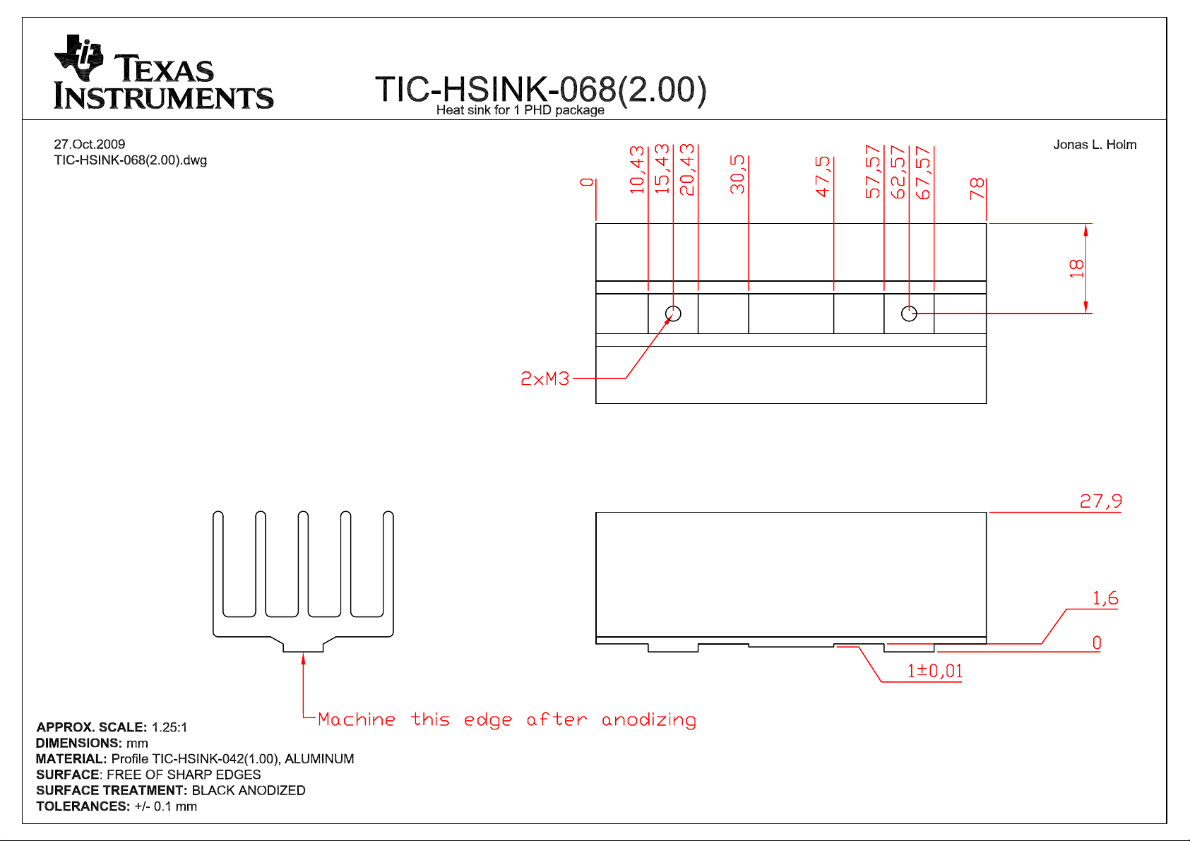
HEATSINK11
HEATSINK11
TIC-HSINK-068_1.00
TIC-HSINK-068_1.00
HEAT SINK
HEAT SINK
M3
M3
C C
B B
A A
M3
SCREW15
SCREW15
M3x6
M3x6
WASHER15
WASHER15
M3
M3
STANDOFF11
STANDOFF11
M3x10
M3x10
5
M3
SCREW16
SCREW16
M3x6
M3x6
WASHER16
WASHER16
M3
M3
STANDOFF12
STANDOFF12
M3x10
M3x10
M3
M3
STANDOFF13
STANDOFF13
M3x10
M3x10
M3
M3
STANDOFF14
STANDOFF14
M3x10
M3x10
4
F11
F11
1
Not Used
Not Used
F12
F12
1
Not Used
Not Used
F13
F13
1
Not Used
Not Used
F14
F14
1
Not Used
Not Used
1
1
1
1
3
GND
JUMPER2
JUMPER2
PCB11
PCB11
A858-PCB-001_1.00
A858-PCB-001_1.00
Black
Black
/ TAS5613 Parts list
/ TAS5613 Parts list
/ TAS5613 Parts list
PCB
PCB
JUMPER1
JUMPER1
Black
Black
AUDIO/IMAGING GROUP
AUDIO/IMAGING GROUP
AUDIO/IMAGING GROUP
Home Audio Amplifiers
Home Audio Amplifiers
Home Audio Amplifiers
ALL RIGHTS RESERVED
ALL RIGHTS RESERVED
TI
TI
TI
TAS5613PHD2EVM
TAS5613PHD2EVM
TAS5613PHD2EVM
Project:
Project:
Project:
Mechanics
Mechanics
Page Title:
Page Title:
Page Title:
File Name:
File Name:
File Name:
Date:
Date:
Date:
2
Mechanics
A858-SCH-001.DSN
A858-SCH-001.DSN
A858-SCH-001.DSN
Wednesday, October 28, 2009 4 4
Wednesday, October 28, 2009 4 4
Wednesday, October 28, 2009 4 4
ALL RIGHTS RESERVED
TEXAS INSTRUMENTS INCORPORATED
TEXAS INSTRUMENTS INCORPORATED
TEXAS INSTRUMENTS INCORPORATED
Jonas L. Holm
Jonas L. Holm
Jonas L. Holm
Engineer:
Engineer:
Engineer:
1
1.00
1.00
1.00
Rev:
Rev:
Rev:
Size:
A4
Size:
A4
Size:
A4
Page: of
Page: of
Page: of
Page 14

TAS5611_13PHD2EVM Parts List (1.00).xls
e
8
r
L
r
L
2
L
L
L
L
6
L
9
a
L
3
s
T
8
K
r
s
T
5
9
r
6
)
r
F
6
)
a
8
)
a
5
)
a
8
-
TI
Qty Part Referenc
6 R53 R54 R55 R56 R57 R5
12 R40 R51 R52 R59 100R / 100mW / 5% / 0603 Thick Film Resistor Yageo RC0603JR-07100RL
1 R49 1.00k / 100mW / 1% / 0603 Thick Film Resistor Yageo RC0603FR-071KL
1 R15 10k / 100mW / 5% / 0603 Thick Film Resisto
4 R62 R66 R68 R7
2 R73 R74 100k / 100mW / 5% / 0603 Thick Film ResistorYageo RC0603JR-07100K
1 R75 10R / 100mW / 5% / 0603 Thick Film ResistorYageo RC0603JR-0710R
1 R48 1.2k / 100mW / 5% / 0603 Thick Film Resistor Yageo RC0603JR-071K2
8 R61 R63 R64 R65 R67 R69 R70 R71 2.2k / 100mW / 5% / 0603 Thick Film Resistor Yageo RC0603JR-072K2L
1 R12 30.0k / 100mW / 1% / 0603 Thick Film Resistor Yageo RC0603FR-0730KL
9 R37 3.3R / 100mW / 5% / 0603 Thick Film Resistor Yageo RC0603JR-073R3L
5 R41 R43 R44 R45 R4
1 R39 47k / 100mW / 5% / 0603 Thick Film Resistor Yageo RC0603JR-0747KL
2 R42 R47 560R / 100mW / 5% / 0603 Thick Film Resistor Yageo RC0603JR-07560RL
1 R50 820R / 100mW / 5% / 0603 Thick Film Resistor Yageo RC0603JR-07820RL
5 C44 C45 C46 C47 C49 Ceramic 10nF / 100V / 20% X7R 0805 Capacitor BC Components 0805B103M101NT
5 C26 C32 C48 C96 C9
1 C11 Ceramic 4.7nF / 50V / 10% X7R 0805 Capacitor BC Components 0805B472K500NT
4 C40 C41 C42 C4
4 C28 C30 C97 C9
1 C50
1 C12 Ceramic 1nF / 50V / 10% NP0 0805 Capacito
C13 C19 C21 C22 C23 C24 C54 C56
12
C62 C65 C79 C84 Ceramic 100nF / 16V / 20% X7R 0603 Capacitor Vishay VJ0603Y104MXJ
4 C25 C27 C29 C31 Ceramic 33nF / 25V / 20% X7R 0603 Capacitor BC Components 0603B333M250NT
5 C58 C59 C60 C72 C73 Ceramic 100pF / 50V / 10% NP0 0603 Capacitor BC Components 0603N101K500NT
2 C67 C68 Ceramic 1nF / 50V / 10% NP0 0603 Capacitor BC Components 0603N102K500NT
4 C77 C78 C82 C83 Ceramic 150pF / 50V / 10% NP0 0603 Capacitor BC Components 0603N151K500NT
1 C20 Ceramic 330pF / 50V / 10% NP0 0603 Capacitor BC Components 0603N331K500NT
2 C75 C76 Ceramic 470pF / 50V / 10% NP0 0603 Capacitor BC Components 0603N471K500NT
4 C37 C38 C39 C52
C14 C15 C16 C17 C18 C53 C55 C63
13
C64 C66 C69 C70 C71
4 C33 C34 C35 C36
1 C85
1 C57
1 C86
1 C61 3.5mm ø8mm FC Series - Low Impedance Panasonic EEUFC1E471L
1 L15
4 L16 L17 L18 L1
1 D18 3A / 60V Schottky 30BQ060 Diode (SMC
3 D13 D14 D1
1 D11 Light Emitting Green Green LED (0603
2 D12 D1
6 Q11 Q12 Q13 Q14 Q15 Q16
1 U11
2 U15 U16
2 U12 U13
1 U17
Description Manufacture First Mfr P/N
0R / 5% / 0603 Thick Film Resisto
10.0k / 100mW / 1% / 0603 Thick Film Resistor Yageo RC0603FR-0710K
4.7k / 100mW / 5% / 0603 Thick Film Resistor Yageo RC0603JR-074K7
Ceramic 1uF / 50V / 10% X7R 0805 CapacitorMurat
Ceramic 1nF / 100V / 10% NP0 1206 CapacitorBC Component
Ceramic 1uF / 50V / 10% X7R 1206 CapacitorTDK C3216X7R1H105
Ceramic 2.2uF / 100V / 20% X7R 1210
Capacitor Murata GRM32ER72A225KA35L
Metal Film 680nF / 250V / 20% Polypropylene
15mm (W:8mm L:18mm) Capacitor Wima MKP 4 0.68uF/20%/250Vdc PCM1
Electrolytic 10uF / 16V / 20% Aluminium 2mm
ø5mm M Series - General Purpose Capacitor Panasonic ECA1CM100
Electrolytic 1000uF / 50V / 20% Aluminium
7.5mm ø16mm FC Series - Low Impedance
Capacitor Panasonic EEUFC1H102
Electrolytic 330uF / 63V / 20% Aluminium 5mm
ø10mm FC Series - Low Impedance Capacitor Panasonic EEUFC1J331L
Electrolytic 47uF / 63V / 20% Aluminium 5mm
ø10mm Capacitor BC Components 2222 136 68479
Electrolytic 470uF / 16V / 20% Aluminium
3.5mm ø8mm Low ESR Capacitor Rubycon 16ZL470M8x16
1mH / 0.55A 20% (1.68R) Ferrite Inductor
(12.8x12.8x8.0) Epcos B82477G4105M000
10uH / Ferrite Inducto
Light Emitting Red Red LED (0603
Light Emitting Yellow Yellow LED (0603
0.115A / 60V N-ch Power 2N7002 Mosfet (SOT
23) Fairchild 2N7002
TAS5611PHD or TAS5613PHD / Stereo Analog
Audio PWM Power Output Stage (PHD64) Texas Instruments TAS5611PHD or TAS5613PHD
OPA1632 / High-Performance, Fully-Differential
Audio Opamp (SO8) Texas Instruments OPA1632D
LM317 / 0.5A Positive Adjustable Regulator
(DCY) Texas Instruments LM317MDCY
TL2575HV-15I / 15V/1-A SIMPLE STEP-DOWN
SWITCHING VOLTAGE REGULATORS (KTT5) Texas Instruments TL2575HV-15IKTTR
Yageo RC0603JR-070R
Yageo RC0603JR-0710K
GRM21BR71H105KA12
1206N102K101N
BC Component
Toko C3B-A033
Int. Rectifie
Toshib
Toshib
Toshib
0805N102K500N
30BQ060PB
TLSU100
TLGU1008
TLYU100
1 of 2
17.Dec. 2009
Page 15

TAS5611_13PHD2EVM Parts List (1.00).xls
h
A
SCREW11 SCREW12 SCREW13
6
SCREW14 SCREW15 SCREW16 M3x6 Pan Head, Pozidriv, A2 Screw Bossard BN 81882 M3x6
WASHER11 WASHER12 WASHER13
6
WASHER14 WASHER15 WASHER16 M3 Stainless Steel Spring Washer Bossard BN 760 M3
STANDOFF11 STANDOFF12
4
STANDOFF13 STANDOFF14 M3x10 Aluminium Stand-off Ettinger 05.03.108
2 J19 J22
2 JUMPER1 JUMPER2
2 J20 J21 Horizontal Female w. Switch Coax Phono socket Chunfeng RJ843-4W
3 J11 J13 J15
2 J24 J25
3 SW1 SW2 SW11 Switch DPDT PCB Mount Switc
1 PCB11
1 HEATSINK11
2 pins / 1 row / 2.54mm Pitch Vertical Male
Friction lock Pin header Header Molex 22-27-2021
2 pins / 1 row / 2.54mm Pitch Horizontal Female
Black Shunt Black Molex 15-29-1024
2 pins / Vertical Female Banana Red and black
banana socket Cliff TPP-3CT
3 pins / 1 row / 2.54mm Pitch Vertical Male
Shunt Header Shunt Header Samtec TSW-107-07-T-T
858-PCB-001_1.00 / TAS5613PHD2EVM2
Printed Circuit Board (ver. 1.00) Elcon A858-PCB-001(1.00)
TIC-HSINK-068_1.00 / Heatsink for 1 PHD
package, length 78 mm Phonotech TIC-HSINK-068(1.00)
NKK-Nikkai G-22-AP
TI
2 of 2
17.Dec. 2009
Page 16

TI A858-PCBSPEC-001(1.00).doc
Jonas Holm
TAS5613PHD2EVM
PCB SPECIFICATION
Version 1.00
BOARD IDENTIFICATION: A858-PCB-001(1.00)
BOARD TYPE: DOUBLE-SIDED PLATED-THROUGH BOARD
LAMINATE TYPE: FR4
LAMINATE THICKNESS: 1.6mm
TOP LAYER COPPER THICKNESS: 70μm (INCL. PLATING EXTERIOR LAYER)
BOTTOM LAYER COPPER THICKNESS: 70μm (INCL. PLATING EXTERIOR LAYER)
COPPER PLATING OF HOLES: >25μm
MINIMUM HOLE DIAMETER 0.3 mm
SILKSCREEN COMPONENT SIDE: WHITE - REMOVE SILKSCREEN FROM SOLDER AREA & PRE-TINNED AREAS
SILKSCREEN SOLDER SIDE: None
SOLDER MASK COMPONENT SIDE: GREEN
SOLDER MASK SOLDER SIDE: GREEN
PROTECTIVE COATING: SOLDER COATING AND CHEMICAL SILVER ON FREE COPPER
ELECTRICAL TEST: PCB MUST BE ELECTRICAL TESTED
MANUFACTURED TO: PERFAG 2E (www.perfag.dk)
APERTURE TABLE: PERFAG 10A (www.perfag.dk)
BOARD SIZE: 95 x 142 mm
Aprox. Number of holes 468
COMMENTS: SEE DRILL INFORMATION FILE (A858-PCB-001(1.00).pdf)
Page 1 of 1
Page 17

Page 18

Page 19
Page 20

Page 21

Page 22
Page 23
Page 24

Page 25
Page 26

Company Confidential
Inductor Specification
DWG no.: TIC-INDC-020(1.00)
Text: 10µH / 5A / 30mΩ
Diagram:
Material:
Wire: ø1.00mm Cu, one layer lacquer, 155°C
Foot-print top view
Lead length: 8mm-12mm, stripped and pre-tinned.
Production: Step 1: N1, 35 turns ø1.00mm cu 2L, start 1, end 2
Step 2: bend and strip/pre-tin leads.
Test: Inductance: pin 1 –2 9 – 11 µH @ 0.1Vrms/10kHz
Release date: 2005-04-12, Jonas Svendsen / Kim Madsen
Core: Micrometals T94-2
1 2
Mechanical:
Texas Instruments Denmark A/S VAT-no. 20 53 16 73
Lyngby Hovedgade 4 Phone: +45 96 34 68 68
DK-2800 Kgs. Lyngby Fax: +45 38 88 78 99
Denmark Web: http:\\www.ti.com
Page 27

IMPORTANT NOTICE
Texas Instruments Incorporated and its subsidiaries (TI) reserve the right to make corrections, modifications, enhancements, improvements,
and other changes to its products and services at any time and to discontinue any product or service without notice. Customers should
obtain the latest relevant information before placing orders and should verify that such information is current and complete. All products are
sold subject to TI’s terms and conditions of sale supplied at the time of order acknowledgment.
TI warrants performance of its hardware products to the specifications applicable at the time of sale in accordance with TI’s standard
warranty. Testing and other quality control techniques are used to the extent TI deems necessary to support this warranty. Except where
mandated by government requirements, testing of all parameters of each product is not necessarily performed.
TI assumes no liability for applications assistance or customer product design. Customers are responsible for their products and
applications using TI components. To minimize the risks associated with customer products and applications, customers should provide
adequate design and operating safeguards.
TI does not warrant or represent that any license, either express or implied, is granted under any TI patent right, copyright, mask work right,
or other TI intellectual property right relating to any combination, machine, or process in which TI products or services are used. Information
published by TI regarding third-party products or services does not constitute a license from TI to use such products or services or a
warranty or endorsement thereof. Use of such information may require a license from a third party under the patents or other intellectual
property of the third party, or a license from TI under the patents or other intellectual property of TI.
Reproduction of TI information in TI data books or data sheets is permissible only if reproduction is without alteration and is accompanied
by all associated warranties, conditions, limitations, and notices. Reproduction of this information with alteration is an unfair and deceptive
business practice. TI is not responsible or liable for such altered documentation. Information of third parties may be subject to additional
restrictions.
Resale of TI products or services with statements different from or beyond the parameters stated by TI for that product or service voids all
express and any implied warranties for the associated TI product or service and is an unfair and deceptive business practice. TI is not
responsible or liable for any such statements.
TI products are not authorized for use in safety-critical applications (such as life support) where a failure of the TI product would reasonably
be expected to cause severe personal injury or death, unless officers of the parties have executed an agreement specifically governing
such use. Buyers represent that they have all necessary expertise in the safety and regulatory ramifications of their applications, and
acknowledge and agree that they are solely responsible for all legal, regulatory and safety-related requirements concerning their products
and any use of TI products in such safety-critical applications, notwithstanding any applications-related information or support that may be
provided by TI. Further, Buyers must fully indemnify TI and its representatives against any damages arising out of the use of TI products in
such safety-critical applications.
TI products are neither designed nor intended for use in military/aerospace applications or environments unless the TI products are
specifically designated by TI as military-grade or "enhanced plastic." Only products designated by TI as military-grade meet military
specifications. Buyers acknowledge and agree that any such use of TI products which TI has not designated as military-grade is solely at
the Buyer's risk, and that they are solely responsible for compliance with all legal and regulatory requirements in connection with such use.
TI products are neither designed nor intended for use in automotive applications or environments unless the specific TI products are
designated by TI as compliant with ISO/TS 16949 requirements. Buyers acknowledge and agree that, if they use any non-designated
products in automotive applications, TI will not be responsible for any failure to meet such requirements.
Following are URLs where you can obtain information on other Texas Instruments products and application solutions:
Products Applications
Amplifiers amplifier.ti.com Audio www.ti.com/audio
Data Converters dataconverter.ti.com Automotive www.ti.com/automotive
DLP® Products www.dlp.com Broadband www.ti.com/broadband
DSP dsp.ti.com Digital Control www.ti.com/digitalcontrol
Clocks and Timers www.ti.com/clocks Medical www.ti.com/medical
Interface interface.ti.com Military www.ti.com/military
Logic logic.ti.com Optical Networking www.ti.com/opticalnetwork
Power Mgmt power.ti.com Security www.ti.com/security
Microcontrollers microcontroller.ti.com Telephony www.ti.com/telephony
RFID www.ti-rfid.com Video & Imaging www.ti.com/video
RF/IF and ZigBee® Solutions www.ti.com/lprf Wireless www.ti.com/wireless
Mailing Address: Texas Instruments, Post Office Box 655303, Dallas, Texas 75265
Copyright © 2009, Texas Instruments Incorporated
 Loading...