

Page 1

TAS5508C
8-Channel Digital Audio PWM Processor
Data Manual
PRODUCTION DATA information is current as of publication date.
Products conform to specifications per the terms of the Texas
Instruments standard warranty. Production processing does not
necessarily include testing of all parameters.
Literature Number: SLES257
September 2010
Page 2

TAS5508C
SLES257–SEPTEMBER 2010
www.ti.com
Contents
1 Introduction PWM ............................................................................................................... 9
1.1 Features ...................................................................................................................... 9
1.2 Overview .................................................................................................................... 10
1.3 TAS5508C System Diagrams ............................................................................................ 12
2 Description ....................................................................................................................... 15
2.1 Physical Characteristics .................................................................................................. 15
2.1.1 Terminal Assignments ......................................................................................... 15
2.1.2 Ordering Information ........................................................................................... 15
2.1.3 PIN Descriptions ................................................................................................ 16
2.2 TAS5508C Functional Description ...................................................................................... 17
2.2.1 Power Supply ................................................................................................... 18
2.2.2 Clock, PLL, and Serial Data Interface ....................................................................... 18
2.2.2.1 Serial Audio Interface .............................................................................. 18
2.2.3 I
2.2.4 Device Control .................................................................................................. 19
2.2.5 Digital Audio Processor (DAP) ................................................................................ 19
2.3 TAS5508C DAP Architecture ............................................................................................ 21
2.3.1 TAS5508C DAP Architecture Diagrams ..................................................................... 21
2.3.2 I
2.4 Input Crossbar Mixer ...................................................................................................... 28
2.5 Biquad Filters .............................................................................................................. 28
2.6 Bass and Treble Controls ................................................................................................ 29
2.7 Volume, Automute, and Mute ............................................................................................ 30
2.8 Automute and Mute ....................................................................................................... 30
2.9 Loudness Compensation ................................................................................................. 31
2.9.1 Loudness Example ............................................................................................. 32
2.10 Dynamic Range Control (DRC) .......................................................................................... 33
2.10.1 DRC Implementation ........................................................................................... 36
2.10.2 Compression/Expansion Coefficient Computation Engine Parameters ................................. 36
2.11 Output Mixer ............................................................................................................... 38
2.12 PWM ........................................................................................................................ 39
2.12.1 DC Blocking (High-Pass Enable/Disable) ................................................................... 40
2.12.2 De-Emphasis Filter ............................................................................................. 40
2.12.3 Power-Supply Volume Control (PSVC) ...................................................................... 40
2.12.4 AM Interference Avoidance ................................................................................... 41
3 TAS5508C Controls and Status ........................................................................................... 43
3.1 I
2
C Status Registers ....................................................................................................... 43
3.1.1 General Status Register (0x01) ............................................................................... 43
2
C Serial-Control Interface ................................................................................... 19
2.2.5.1 TAS5508C Audio-Processing Configurations .................................................. 19
2.2.5.2 TAS5508C Audio Signal-Processing Functions ................................................ 20
2
C Coefficient Number Formats ............................................................................. 24
2.3.2.1 28-Bit 5.23 Number Format ....................................................................... 24
2.3.2.2 48-Bit 25.23 Number Format ..................................................................... 26
2.3.2.3 TAS5508C Audio Processing .................................................................... 27
2.10.2.1 Threshold Parameter Computation .............................................................. 37
2.10.2.2 Offset Parameter Computation ................................................................... 37
2.10.2.3 Slope Parameter Computation ................................................................... 38
2 Contents Copyright © 2010, Texas Instruments Incorporated
Page 3

TAS5508C
www.ti.com
SLES257–SEPTEMBER 2010
3.1.2 Error Status Register (0x02) .................................................................................. 43
3.2 TAS5508C Pin Controls .................................................................................................. 43
3.2.1 Reset (RESET) ................................................................................................. 43
3.2.2 Power Down (PDN) ............................................................................................ 45
3.2.3 Back-End Error (BKND_ERR) ................................................................................ 46
3.2.4 Speaker/Headphone Selector (HP_SEL) .................................................................... 46
3.2.5 Mute (MUTE) .................................................................................................... 46
3.3 Device Configuration Controls ........................................................................................... 47
3.3.1 Channel Configuration Registers ............................................................................. 47
3.3.2 Headphone Configuration Registers ......................................................................... 48
3.3.3 Audio System Configurations ................................................................................. 48
3.3.3.1 Using Line Outputs in 6-Channel Configurations .............................................. 49
3.3.4 Recovery from Clock Error .................................................................................... 49
3.3.5 Power-Supply Volume-Control Enable ....................................................................... 49
3.3.6 Volume and Mute Update Rate ............................................................................... 49
3.3.7 Modulation Index Limit ......................................................................................... 50
3.3.8 Interchannel Delay .............................................................................................. 50
3.4 Master Clock and Serial Data Rate Controls .......................................................................... 50
3.4.1 PLL Operation ................................................................................................... 51
3.5 Bank Controls .............................................................................................................. 51
3.5.1 Manual Bank Selection ........................................................................................ 52
3.5.2 Automatic Bank Selection ..................................................................................... 52
3.5.2.1 Coefficient Write Operations While Automatic Bank Switch Is Enabled .................... 52
3.5.3 Bank Set ......................................................................................................... 52
3.5.4 Bank-Switch Timeline .......................................................................................... 52
3.5.5 Bank-Switching Example 1 .................................................................................... 53
3.5.6 Bank-Switching Example 2 .................................................................................... 53
4 Electrical Specifications ..................................................................................................... 55
4.1 Absolute Maximum Ratings .............................................................................................. 55
4.2 Dissipation Rating Table (High-k Board, 105°C Junction) ........................................................... 55
4.3 Dynamic Performance At Recommended Operating Conditions at 25°C .......................................... 55
4.4 Recommended Operating Conditions .................................................................................. 55
4.5 Electrical Characteristics ................................................................................................. 56
4.6 PWM Operation ............................................................................................................ 56
4.7 Switching Characteristics ................................................................................................. 56
4.7.1 Clock Signals .................................................................................................... 56
4.7.2 Serial Audio Port ................................................................................................ 57
4.7.3 I
4.7.4 Reset Timing (RESET) ......................................................................................... 59
4.7.5 Power-Down (PDN) Timing ................................................................................... 59
4.7.6 Back-End Error (BKND_ERR) ................................................................................ 60
4.7.7 Mute Timing (MUTE) ........................................................................................... 60
4.7.8 Headphone Select (HP_SEL) ................................................................................. 61
4.7.9 Volume Control ................................................................................................. 62
4.8 Serial Audio Interface Control and Timing ............................................................................. 62
4.8.1 I
4.8.2 Left-Justified Timing ............................................................................................ 63
2
C Serial Control Port Operation ............................................................................. 58
2
S Timing ....................................................................................................... 62
Copyright © 2010, Texas Instruments Incorporated Contents 3
Page 4

TAS5508C
SLES257–SEPTEMBER 2010
www.ti.com
4.8.3 Right-Justified Timing .......................................................................................... 64
5 I
2
C Serial-Control Interface (Slave Address 0x36) .................................................................. 65
5.1 General I
2
C Operation .................................................................................................... 65
5.2 Single- and Multiple-Byte Transfers ..................................................................................... 65
5.3 Single-Byte Write .......................................................................................................... 66
5.4 Multiple-Byte Write ........................................................................................................ 66
5.5 Incremental Multiple-Byte Write ......................................................................................... 67
5.6 Single-Byte Read .......................................................................................................... 67
5.7 Multiple-Byte Read ........................................................................................................ 68
6 Serial-Control I
2
C Register Summary ................................................................................... 69
7 Serial-Control Interface Register Definitions ......................................................................... 73
7.1 Clock Control Register (0x00) ........................................................................................... 73
7.2 General Status Register 0 (0x01) ....................................................................................... 73
7.3 Error Status Register (0x02) ............................................................................................. 74
7.4 System Control Register 1 (0x03) ....................................................................................... 74
7.5 System Control Register 2 (0x04) ....................................................................................... 74
7.6 Channel Configuration Control Registers (0x05–0x0C) .............................................................. 74
7.7 Headphone Configuration Control Register (0x0D) ................................................................... 75
7.8 Serial Data Interface Control Register (0x0E) ......................................................................... 75
7.9 Soft Mute Register (0x0F) ................................................................................................ 76
7.10 Automute Control Register (0x14) ....................................................................................... 77
7.11 Automute PWM Threshold and Back-End Reset Period Register (0x15) .......................................... 78
7.12 Modulation Index Limit Register (0x16) ................................................................................. 79
7.13 Interchannel Delay Registers (0x1B–0x22) ............................................................................ 79
7.14 Channel Offset Register (0x23) .......................................................................................... 79
7.15 Bank-Switching Command Register (0x40) ............................................................................ 80
7.16 Input Mixer Registers, Channels 1–8 (0x41–0x48) ................................................................... 80
7.17 Bass Management Registers (0x49–0x50) ............................................................................ 84
7.18 Biquad Filter Register (0x51–0x88) ..................................................................................... 84
7.19 Bass and Treble Bypass Register, Channels 1–8 (0x89–0x90) ..................................................... 85
7.20 Loudness Registers (0x91–0x95) ....................................................................................... 85
7.21 DRC1 Control Registers, Channels 1–7 (0x96) ....................................................................... 86
7.22 DRC2 Control Register, Channel 8 (0x97) ............................................................................. 87
7.23 DRC1 Data Registers (0x98–0x9C) ..................................................................................... 87
7.24 DRC2 Data Registers (0x9D–0xA1) .................................................................................... 88
7.25 DRC Bypass Registers (0xA2–0xA9) ................................................................................... 88
7.26 8×2 Output Mixer Registers (0xAA–0xAF) ............................................................................. 88
7.27 8×3 Output Mixer Registers (0xB0–0xB1) ............................................................................. 89
7.28 Volume Biquad Register (0xCF) ......................................................................................... 91
7.29 Volume, Treble, and Bass Slew Rates Register (0xD0) ............................................................. 92
7.30 Volume Registers (0xD1–0xD9) ......................................................................................... 92
7.31 Bass Filter Set Register (0xDA) ......................................................................................... 94
7.32 Bass Filter Index Register (0xDB) ....................................................................................... 95
7.33 Treble Filter Set Register (0xDC) ....................................................................................... 96
7.34 Treble Filter Index (0xDD) ................................................................................................ 97
7.35 AM Mode Register (0xDE) ............................................................................................... 97
4 Contents Copyright © 2010, Texas Instruments Incorporated
Page 5

TAS5508C
www.ti.com
7.36 PSVC Range Register (0xDF) ........................................................................................... 99
7.37 General Control Register (0xE0) ........................................................................................ 99
7.38 Incremental Multiple-Write Append Register (0xFE) .................................................................. 99
SLES257–SEPTEMBER 2010
8 TAS5508C Example Application Schematic ......................................................................... 101
Copyright © 2010, Texas Instruments Incorporated Contents 5
Page 6

TAS5508C
SLES257–SEPTEMBER 2010
www.ti.com
List of Figures
1-1 TAS5508C Functional Structure................................................................................................ 12
1-2 Typical TAS5508C Application (DVD Receiver) ............................................................................. 12
1-3 Recommended TAS5508C and TAS5121 Channel Configuraton......................................................... 13
2-1 TAS5508C DAP Architecture With I
2-2 TAS5508C Architecture With I
2-3 TAS5508C Detailed Channel Processing..................................................................................... 24
2-4 5.23 Format ....................................................................................................................... 25
2-5 Conversion Weighting Factors—5.23 Format to Floating Point............................................................ 25
2-6 Alignment of 5.23 Coefficient in 32-Bit I
2-7 25.23 Format...................................................................................................................... 26
2-8 Alignment of 5.23 Coefficient in 32-Bit I
2-9 Alignment of 25.23 Coefficient in Two 32-Bit I
2-10 TAS5508C Digital Audio Processing .......................................................................................... 28
2-11 Input Crossbar Mixer............................................................................................................. 28
2-12 Biquad Filter Structure........................................................................................................... 29
2-13 Automute Threshold ............................................................................................................. 31
2-14 Loudness Compensation Functional Block Diagram ........................................................................ 32
2-15 Loudness Example Plots........................................................................................................ 33
2-16 DRC Positioning in TAS5508C Processing Flow ............................................................................ 34
2-17 Dynamic Range Compression (DRC) Transfer Function Structure........................................................ 35
2-18 Output Mixers..................................................................................................................... 39
2-19 De-Emphasis Filter Characteristics............................................................................................ 40
2-20 Power-Supply and Digital Gains (Log Space)................................................................................ 41
2-21 Power-Supply and Digital Gains (Linear Space)............................................................................. 41
2-22 Block Diagrams of Typical Systems Requiring TAS5508C Automatic AM Interference-Avoidance Circuit .......... 42
4-1 Slave Mode Serial Data Interface Timing..................................................................................... 57
4-2 SCL and SDA Timing............................................................................................................ 58
4-3 Start and Stop Conditions Timing.............................................................................................. 58
4-4 Reset Timing...................................................................................................................... 59
4-5 Power-Down Timing ............................................................................................................. 59
4-6 Error Recovery Timing........................................................................................................... 60
4-7 Mute Timing....................................................................................................................... 60
4-8 HP_SEL Timing................................................................................................................... 62
4-9 I
2
S 64-Fs Format................................................................................................................. 63
4-10 Left-Justified 64-Fs Format ..................................................................................................... 63
4-11 Right-Justified 64-Fs Format.................................................................................................... 64
5-1 Typical I
2
C Sequence............................................................................................................ 65
5-2 Single-Byte Write Transfer ...................................................................................................... 66
5-3 Multiple-Byte Write Transfer .................................................................................................... 67
5-4 Single-Byte Read Transfer...................................................................................................... 68
5-5 Multiple-Byte Read Transfer .................................................................................................... 68
2
C Registers (Fs ≤ 96 kHz)........................................................... 23
2
C Registers (Fs = 176.4 kHz or Fs = 192 kHz) ......................................... 24
2
C Word............................................................................. 25
2
C Word............................................................................. 26
2
C Words.................................................................... 27
6 List of Figures Copyright © 2010, Texas Instruments Incorporated
Page 7

TAS5508C
www.ti.com
SLES257–SEPTEMBER 2010
List of Tables
2-1 Serial Data Formats.............................................................................................................. 19
2-2 TAS5508C Audio Processing Feature Sets .................................................................................. 21
2-3 Contents of One 20-Byte Biquad Filter Register (Default = All-Pass)..................................................... 29
2-4 Bass and Treble Filter Selections.............................................................................................. 30
2-5 Linear Gain Step Size ........................................................................................................... 30
2-6 Default Loudness Compensation Parameters................................................................................ 32
2-7 Loudness Function Parameters ................................................................................................ 33
2-8 DRC Recommended Changes From TAS5508C Defaults ................................................................. 34
3-1 Device Outputs During Reset................................................................................................... 43
3-2 Values Set During Reset ........................................................................................................ 44
3-3 Device Outputs During Power Down .......................................................................................... 45
3-4 Device Outputs During Back-End Error ....................................................................................... 46
3-5 Description of the Channel Configuration Registers (0x05 to 0x0C) ...................................................... 47
3-6 Recommended TAS5508C Configurations for Texas Instruments Power Stages....................................... 48
3-7 Audio System Configuration (General Control Register 0xE0)............................................................. 49
3-8 Volume Ramp Rates in ms ..................................................................................................... 50
3-9 Interchannel Delay Default Values............................................................................................. 50
7-1 Clock Control Register Format ................................................................................................. 73
7-2 General Status Register Format................................................................................................ 73
7-3 Error Status Register Format ................................................................................................... 74
7-4 System Control Register 1 Format............................................................................................. 74
7-5 System Control Register 2 Format............................................................................................. 74
7-6 Channel Configuration Control Register Format ............................................................................. 75
7-7 Headphone Configuration Control Register Format ......................................................................... 75
7-8 Serial Data Interface Control Register Format ............................................................................... 75
7-9 Soft Mute Register Format...................................................................................................... 76
7-10 Automute Control Register Format............................................................................................. 77
7-11 Automute PWM Threshold and Back-End Reset Period Register Format................................................ 78
7-12 Modulation Index Limit Register Format ...................................................................................... 79
7-13 Interchannel Delay Register Format ........................................................................................... 79
7-14 Channel Offset Register Format................................................................................................ 79
7-15 Bank-Switching Command Register Format.................................................................................. 80
7-16 Channel 1–8 Input Mixer Register Format.................................................................................... 81
7-17 Bass Management Register Format ........................................................................................... 84
7-18 Biquad Filter Register Format .................................................................................................. 84
7-19 Contents of One 20-Byte Biquad Filter Register (Default = All-Pass)..................................................... 85
7-20 Channel 1–8 Bass and Treble Bypass Register Format.................................................................... 85
7-21 Loudness Register Format...................................................................................................... 85
7-22 Channel 1–7 DCR1 Control Register Format................................................................................. 86
7-23 Channel-8 DRC2 Control Register Format ................................................................................... 87
7-24 DRC1 Data Register Format.................................................................................................... 87
7-25 DRC2 Data Register Format.................................................................................................... 88
7-26 DRC Bypass Register Format .................................................................................................. 88
7-27 Output Mixer Register Format (Upper 4 Bytes) .............................................................................. 89
7-28 Output Mixer Register Format (Lower 4 Bytes) .............................................................................. 89
7-29 Output Mixer Register Format (Upper 4 Bytes) .............................................................................. 90
7-30 Output Mixer Register Format (Middle 4 Bytes).............................................................................. 90
Copyright © 2010, Texas Instruments Incorporated List of Tables 7
Page 8

TAS5508C
SLES257–SEPTEMBER 2010
7-31 Output Mixer Register Format (Lower 4 Bytes) .............................................................................. 90
7-32 Volume Biquad Register Format (Default = All-Pass)....................................................................... 91
7-33 Volume Gain Update Rate (Slew Rate) ....................................................................................... 92
7-34 Treble and Bass Gain Step Size (Slew Rate)................................................................................ 92
7-35 Volume Register Format ........................................................................................................ 92
7-36 Master and Individual Volume Controls ....................................................................................... 93
7-37 Channel 8 (Subwoofer).......................................................................................................... 94
7-38 Channels 6 and 5 (Right and Left Lineout in 6-Channel Configuration; Right and Left Surround in 8-Channel
Configuration)..................................................................................................................... 94
7-39 Channels 4 and 3 (Right and Left Rear) ...................................................................................... 94
7-40 Channels 7, 2, and 1 (Center, Right Front, and Left Front)................................................................. 95
7-41 Bass Filter Index Register Format ............................................................................................. 95
7-42 Bass Filter Indexes............................................................................................................... 95
7-43 Channel 8 (Subwoofer).......................................................................................................... 96
7-44 Channels 6 and 5 (Right and Left Lineout in 6-Channel Configuration; Right and Left Surround in 8-Channel
Configuration)..................................................................................................................... 96
7-45 Channels 4 and 3 (Right and Left Rear) ...................................................................................... 96
7-46 Channels 7, 2, and 1 (Center, Right Front, and Left Front)................................................................. 96
7-47 Treble Filter Index Register Format............................................................................................ 97
7-48 Treble Filter Indexes............................................................................................................. 97
7-49 AM Mode Register Format ...................................................................................................... 97
7-50 AM Tuned Frequency Register in BCD Mode (Lower 2 Bytes of 0xDE).................................................. 98
7-51 AM Tuned Frequency Register in Binary Mode (Lower 2 Bytes of 0xDE)................................................ 98
7-52 PSVC Range Register Format ................................................................................................. 99
7-53 General Control Register Format .............................................................................................. 99
www.ti.com
8 List of Tables Copyright © 2010, Texas Instruments Incorporated
Page 9

TAS5508C
www.ti.com
8-Channel Digital Audio PWM Processor
Check for Samples: TAS5508C
1 Introduction PWM
1.1 Features
1234
• General Features
– Automated Operation With an Easy-to-Use
Control Interface
– I2C Serial-Control Slave Interface
– Integrated AM Interference-Avoidance
Circuitry
– Single, 3.3-V Power Supply
– 64-Pin TQFP Package
– 5-V Tolerant Inputs
• Audio Input/Output
– Automatic Master Clock Rate and Data
Sample Rate Detection
– Eight Serial Audio Input Channels
– Eight PWM Audio Output Channels
Configurable as Six Channels With Stereo
Lineout or Eight Channels
– Line Output Is a PWM Output to Drive an
External Differential-Input Operational
Amplifier
– Headphone PWM Output to Drive an External
Differential Amplifier Like the TPA112
– PWM Outputs Support Single-Ended and
Bridge-Tied Loads
– 32-, 38-, 44.1-, 48-, 88.2-, 96-, 176.4-, and
192-kHz Sampling Rates
– Data Formats: 16-, 20-, or 24-Bit
Left-Justified, I2S, or Right-Justified Input
Data
– 64-Fs Bit-Clock Rate
– 128-, 192-, 256-, 384-, 512-, and 768-Fs
Master Clock Rates (Up to a Maximum of
50 MHz)
• Audio Processing
– 48-Bit Processing Architecture With 76 Bits
of Precision for Most Audio Processing
Features
– Volume Control Range 36 dB to –127 dB
• Master Volume Control Range of 18 dB to
–100 dB
• Eight Individual Channel Volume Control
Ranges of 18 dB to –127 dB
– Programmable Soft Volume and Mute
1
Please be aware that an important notice concerning availability, standard warranty, and use in critical applications of Texas
Instruments semiconductor products and disclaimers thereto appears at the end of this data sheet.
2PurePath Digital is a trademark of Texas Instruments.
3Matlab is a trademark of Math Works, Inc.
4All other trademarks are the property of their respective owners.
PRODUCTION DATA information is current as of publication date.
Products conform to specifications per the terms of the Texas
Instruments standard warranty. Production processing does not
necessarily include testing of all parameters.
SLES257–SEPTEMBER 2010
Update Rates
– Four Bass and Treble Tone Controls with
±18-dB Range, Selectable Corner
Frequencies, and Second-Order Slopes
• L, R, and C
• LS, RS
• LR, RR
• Sub
– Configurable Loudness Compensation
– Two Dynamic Range Compressors With Two
Thresholds, Two Offsets, and Three Slopes
– Seven Biquads Per Channel
– Full 8×8 Input Crossbar Mixer. Each
Signal-Processing Channel Input Can Be
Any Ratio of the Eight Input Channels.
– 8×2 Output Mixer – Channels 1–6. Each
Output Can Be Any Ratio of Any Two
Signal-Processed Channels.
– 8×3 Output Mixer – Channels 7 and 8. Each
Output Can Be Any Ratio of Any Three
Signal-Processed Channels.
– Three Coefficient Sets Stored on the Device
Can Be Selected Manually or Automatically
(Based on Specific Data Rates).
– DC Blocking Filters
– Able to Support a Variety of Bass
Management Algorithms
• PWM Processing
– 32-Bit Processing PWM Architecture With 40
Bits of Precision
– 8× Oversampling With Fifth-Order Noise
Shaping at 32 kHz–48 kHz, 4× Oversampling
at 88.2 kHz and 96 kHz, and 2× Oversampling
at 176.4 kHz and 192 kHz
– >102-dB Dynamic Range
– THD+N < 0.1%
– 20-Hz–20-kHz, Flat Noise Floor for 44.1-, 48-,
88.2-, 96-, 176.4-, and 192-kHz Data Rates
– Digital De-Emphasis for 32-, 44.1-, and
48-kHz Data Rates
– Flexible Automute Logic With Programmable
Threshold and Duration for Noise-Free
Copyright © 2010, Texas Instruments Incorporated
Page 10

TAS5508C
SLES257–SEPTEMBER 2010
Operation Support for Enhanced Dynamic Range in
– Intelligent AM Interference-Avoidance
High-Performance Applications
System Provides Clear AM Reception – Adjustable Modulation Limit
– Power-Supply Volume Control (PSVC)
1.2 Overview
The TAS5508C is an 8-channel digital pulse-width modulator (PWM) that provides both advanced
performance and a high level of system integration. The TAS5508C is designed to interface seamlessly
with most audio digital signal processors. The TAS5508C automatically adjusts control configurations in
response to clock and data rate changes and idle conditions. This enables the TAS5508C to provide an
easy-to-use control interface with relaxed timing requirements.
The TAS5508C can drive eight channels of H-bridge power stages. Texas Instruments H-bridge parts
TAS5111, TAS5112, or TAS5182 with FETs are designed to work seamlessly with the TAS5508C. The
TAS5508C supports both single-ended or bridge-tied load configurations. The TAS5508C also provides a
high-performance, differential output to drive an external, differential-input, analog headphone amplifier
(such as the TPA112).
The TAS5508C uses AD modulation operating at a 384-kHz switching rate for 48-, 96-, and 192-kHz data.
The 8× oversampling combined with the fifth-order noise shaper provides a broad, flat noise floor and
excellent dynamic range from 20 Hz to 20 kHz.
The TAS5508C is a clocked slave-only device. The TAS5508C receives MCLK, SCLK, and LRCLK from
other system components. The TAS5508C accepts master clock rates of 128, 192, 256, 384, 512, and
768 Fs. The TAS5508C accepts a 64-Fs bit clock.
www.ti.com
The TAS5508C allows for extending the dynamic range by providing a power-supply volume control
(PSVC) output signal.
10 Introduction PWM Copyright © 2010, Texas Instruments Incorporated
Submit Documentation Feedback
Product Folder Link(s): TAS5508C
Page 11
PWM_HPP and MR
PWM_HPP and ML
MCLK
XTL_OUT
XTL_IN
PLL_FLTM
PLL_FLTP
OSC CAP
SCLK
LRCLK
SDIN1
SDIN2
SDIN3
SDIN4
SDA
SCL
RESET
PDN
MUTE
HP_SEL
BKND_ERR
PWM Section
PWM AP and AM7 Center
PWM AP and AM4 R Rear
PWM AP and AM3 L Rear
PWM AP and AM8
Subwoofer
PWM AP and AM1 L Front
PWM AP and AM2 R Front
Power Supply
PWM AP and AM5 L Surround
PWM L Lineout
PWM AP and AM6 R Surround
PWM R Lineout
Digital Audio Processor
VALID
Device
Control
8
8
4 2
0
Det
88
PSVC
9
2
PSVC
Volume
Control
Clock, PLL, and Serial Data I/F
I
2
C
Serial
Control
I/F
VR_PLL
AVDD_PLL
AVSS_PLL
AVDD_REF
VBGAP
VRA_PLL
VRD_PLL
DVDD
DVSS
AVDD
System Control
DAP Control PWM Control
8 × 8 Crossbar Mixer
7
Biquads
DC
Block
De
Emph
SRC NS PWM
0
Det
7
Biquads
DRC
Loud
Comp
Soft
Tone
DC
Block
De
Emph
SRC NS PWM
8 × 2 Crossbar Mixer
0
Det
7
Biquads
DRC
Loud
Comp
Soft
Tone
DC
Block
De
Emph
SRC NS PWM
0
Det
7
Biquads
DRC
Loud
Comp
Soft
Tone
DC
Block
De
Emph
SRC NS PWM
0
Det
7
Biquads
DRC
Loud
Comp
Soft
Tone
DC
Block
De
Emph
SRC NS PWM
0
Det
7
Biquads
DRC
Loud
Comp
Soft
Tone
DC
Block
De
Emph
SRC NS PWM
0
Det
7
Biquads
DRC
Loud
Comp
Soft
Tone
DC
Block
De
Emph
SRC NS PWM
0
Det
7
Biquads
DRC
Loud
Comp
Soft
Tone
DC
Block
De
Emph
Interpolate SRC NS PWM
Soft
Tone
DRC
Loud
Comp
Output Control
Interpolate
Interpolate
Interpolate
Interpolate
Interpolate
Interpolate
Interpolate
B0011-01
AVSS
Soft
Vol
Soft
Vol
Soft
Vol
Soft
Vol
Soft
Vol
Soft
Vol
Soft
Vol
Soft
Vol
8
TAS5508C
www.ti.com
SLES257–SEPTEMBER 2010
Figure 1-1. TAS5508C Functional Structure
Copyright © 2010, Texas Instruments Incorporated Introduction PWM 11
Submit Documentation Feedback
Product Folder Link(s): TAS5508C
Page 12
T AS5508C
DVDLoader
PowerSupply
T exasInstruments
DigitalAudioAmplifier
MPEGDecoder
Front-PanelControls
AM
FM
T uner
TAS5508C
SLES257–SEPTEMBER 2010
1.3 TAS5508C System Diagrams
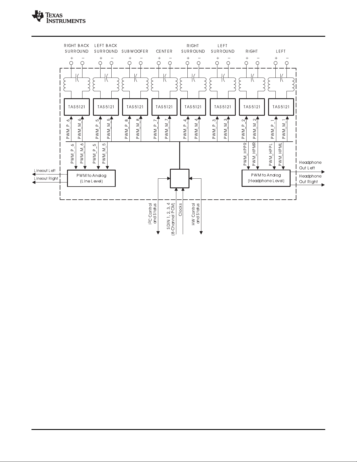
Typical applications for the TAS5508C are 6- to 8-channel audio systems such as DVD or AV receivers.
Figure 1-2 shows the basic system diagram of the DVD receiver.
Figure 1-2. Typical TAS5508C Application (DVD Receiver)
www.ti.com
Figure 1-3 shows the recommended channel configuration when using the TAS5508C with the TAS5121
power stage. Note that each channel is normally dedicated to a particular function.
12 Introduction PWM Copyright © 2010, Texas Instruments Incorporated
Submit Documentation Feedback
Product Folder Link(s): TAS5508C
Page 13
TAS5508C
TAS5508C
www.ti.com
SLES257–SEPTEMBER 2010
Figure 1-3. Recommended TAS5508C and TAS5121 Channel Configuraton
Copyright © 2010, Texas Instruments Incorporated Introduction PWM 13
Submit Documentation Feedback
Product Folder Link(s): TAS5508C
Page 14

TAS5508C
SLES257–SEPTEMBER 2010
www.ti.com
14 Introduction PWM Copyright © 2010, Texas Instruments Incorporated
Submit Documentation Feedback
Product Folder Link(s): TAS5508C
Page 15
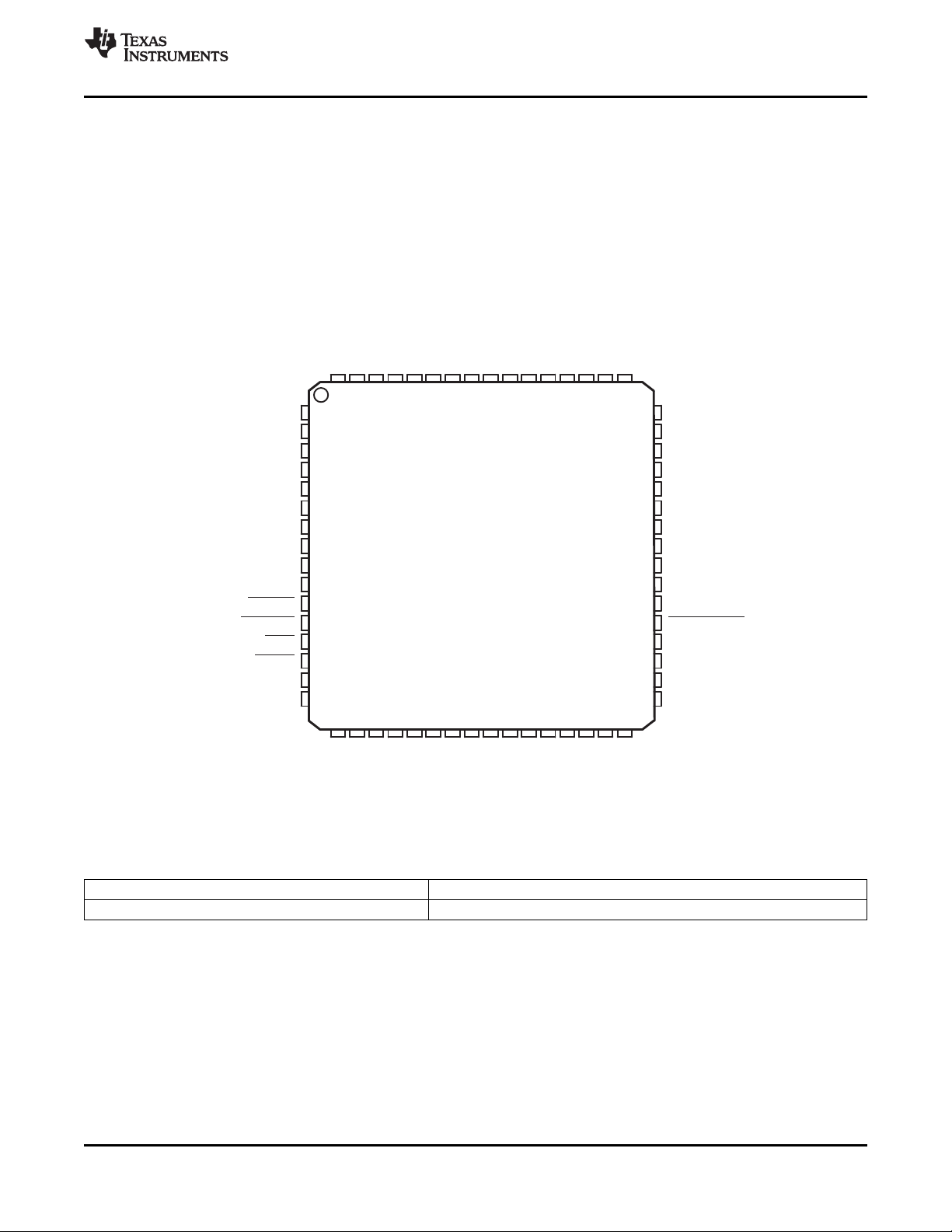
17
VR_PWM
PWM_P_4
PWM_M_4
PWM_P_3
PWM_M_3
PWM_P_2
PWM_M_2
PWM_P_1
PWM_M_1
VALID
DVSS
BKND_ERR
DVDD
DVSS
DVSS
VR_DIG
48
47
46
45
44
43
42
41
40
39
38
37
36
35
34
33
1
2
3
4
5
6
7
8
9
10
11
12
13
14
15
16
VRA_PLL
PLL_FLT_RET
PLL_FLTM
PLL_FLTP
AVSS
AVSS
VRD_PLL
AVSS_PLL
AVDD_PLL
VBGAP
RESET
HP_SEL
PDN
MUTE
DVDD
DVSS
18 19 20 21 22 23 24 25 26 27 28 29 30 31 32
64 63 62 61 60 59 58 57 56 55 54 53 52 51 50 49
PAG PACKAGE
(TOP VIEW)
VR_DPLL
OSC_CAP
XTL_OUT
XTL_IN
RESERVED
RESERVED
RESERVED
SDA
SCL
LRCLK
SCLK
SDIN4
SDIN3
SDIN2
SDIN1
PSVC
RESEVED
MCLK
PWM_HPPR
PWM_HPMR
PWM_HPPL
PWM_HPML
PWM_P_6
PWM_M_6
PWM_P_5
PWM_M_5
DVDD_PWM
DVSS_PWM
PWM_P_8
PWM_M_8
PWM_P_7
PWM_M_7
P0010-01
TAS5508C
www.ti.com
2 Description
2.1 Physical Characteristics
2.1.1 Terminal Assignments
SLES257–SEPTEMBER 2010
2.1.2 Ordering Information
T
A
0°C to 70°C TAS5508CPAG
PLASTIC 64-PIN PQFP (PN)
Copyright © 2010, Texas Instruments Incorporated Description 15
Product Folder Link(s): TAS5508C
Submit Documentation Feedback
Page 16
TAS5508C
SLES257–SEPTEMBER 2010
www.ti.com
2.1.3 PIN Descriptions
PIN
NAME NO.
AVDD_PLL 9 P 3.3-V analog power supply for PLL. This terminal can be connected to the same
AVSS 5, 6 P Analog ground
AVSS_PLL 8 P Analog ground for PLL. This terminal should reference the same ground as
BKND_ERR 37 DI Pullup Active-low. A back-end error sequence is generated by applying logic low to this
DVDD 15, 36 P 3.3-V digital power supply
DVDD_PWM 54 P 3.3-V digital power supply for PWM
DVSS 16, 34, P Digital ground
35, 38
DVSS_PWM 53 P Digital ground for PWM
HP_SEL 12 DI 5 V Pullup Headphone in/out selector. When a logic low is applied, the headphone is
LRCLK 26 DI 5 V Serial-audio data left/right clock (sampling-rate clock)
MCLK 63 DI 5 V Pulldown MCLK is a 3.3-V master clock input. The input frequency of this clock can range
MUTE 14 DI 5 V Pullup Soft mute of outputs, active-low (muted signal = a logic low, normal operation =
OSC_CAP 18 AO Oscillator capacitor
PDN 13 DI 5 V Pullup Power down, active-low. PDN powers down all logic and stops all clocks
PLL_FLT_RET 2 AO PLL external filter return
PLL_FLTM 3 AO PLL negative input. Connected to PLL_FLT_RTN via an RC network
PLL_FLTP 4 AI PLL positive input. Connected to PLL_FLT_RTN via an RC network
PSVC 32 O Power-supply volume control PWM output
PWM_HPML 59 DO PWM left-channel headphone (differential –)
PWM_HPMR 61 DO PWM right-channel headphone (differential –)
PWM_HPPL 60 DO PWM left-channel headphone (differential +)
PWM_HPPR 62 DO PWM right-channel headphone (differential +)
PWM_M_1 40 DO PWM 1 output (differential –)
PWM_M_2 42 DO PWM 2 output (differential –)
PWM_M_3 44 DO PWM 3 output (differential –)
PWM_M_4 46 DO PWM 4 output (differential –)
PWM_M_5 55 DO PWM 5 output (differential –)
PWM_M_6 57 DO PWM 6 output (differential –)
PWM_M_7 49 DO PWM 7 (lineout L) output (differential –)
PWM_M_8 51 DO PWM 8 (lineout R) output (differential –)
PWM_P_1 41 DO PWM 1 output (differential +)
PWM_P_2 43 DO PWM 2 output (differential +)
PWM_P_3 45 DO PWM 3 output (differential +)
PWM_P_4 47 DO PWM 4 output (differential +)
TYPE
(1)
5-V
TOLERANT
TERMINATION
(2)
power source used to drive power terminal DVDD, but to achieve low PLL jitter,
this terminal should be bypassed to AVSS_PLL with a 0.1-mF low-ESR
capacitor.
terminal DVSS, but to achieve low PLL jitter, ground noise at this terminal must
be minimized. The availability of the AVSS terminal allows a designer to use
optimizing techniques such as star ground connections, separate ground planes,
or other quiet ground-distribution techniques to achieve a quiet ground reference
at this terminal.
terminal. The BKND_ERR results in no change to any system parameters, with
all H-bridge drive signals going to a hard-mute (M) state.
selected (speakers are off). When a logic high is applied, speakers are selected
(headphone is off).
from 4 MHz to 50 MHz.
a logic high). The mute control provides a noiseless volume ramp to silence.
Releasing mute provides a noiseless ramp to previous volume.
whenever a logic low is applied. The internal parameters are preserved through
a power-down cycle, as long as RESET is not active. The duration for system
recovery from power down is 100 ms.
DESCRIPTION
(1) Type: A = analog; D = 3.3-V digital; P = power/ground/decoupling; I = input; O = output
(2) All pullups are 200-mA weak pullups and all pulldowns are 200-mA weak pulldowns. The pullups and pulldowns are included to ensure
proper input logic levels if the terminals are left unconnected (pullups => logic-1 input; pulldowns => logic-0 input). Devices that drive
inputs with pullups must be able to sink 200 mA, while maintaining a logic-0 drive level. Devices that drive inputs with pulldowns must be
able to source 200 mA, while maintaining a logic-1 drive level.
16 Description Copyright © 2010, Texas Instruments Incorporated
Submit Documentation Feedback
Product Folder Link(s): TAS5508C
Page 17
TAS5508C
www.ti.com
PIN
NAME NO.
PWM_P_5 56 DO PWM 5 output (differential +)
PWM_P_6 58 DO PWM 6 output (differential +)
PWM_P_7 50 DO PWM 7 (lineout L) output (differential +)
PWM_P_8 52 DO PWM 8 (lineout R) output (differential +)
RESERVED 21, 22, Connect to digital ground
23, 64
RESET 11 DI 5 V Pullup System reset input, active-low. A system reset is generated by applying a logic
SCL 25 DI 5 V
SCLK 27 DI 5 V Serial-audio data clock (shift clock) input
SDA 24 DIO 5 V
SDIN1 31 DI 5 V Pulldown Serial-audio data input 1 is one of the serial-data input ports. SDIN1 supports
SDIN2 30 DI 5 V Pulldown Serial-audio data input 2 is one of the serial-data input ports. SDIN2 supports
SDIN3 29 DI 5 V Pulldown Serial-audio data input 3 is one of the serial-data input ports. SDIN3 supports
SDIN4 28 DI 5 V Pulldown Serial-audio data input 4 is one of the serial-data input ports. SDIN4 supports
VALID 39 DO Output indicating validity of PWM outputs, active-high
VBGAP 10 P Band-gap voltage reference. A pinout of the internally regulated 1.2-V reference.
VR_DIG 33 P Voltage reference for 1.8-V digital core supply. A pinout of the internally
VR_DPLL 17 P Voltage reference for 1.8-V digital PLL supply. A pinout of the internally
VR_PWM 48 P Voltage reference for 1.8-V digital PWM core supply. A pinout of the internally
VRA_PLL 1 P Voltage reference for 1.8-V PLL analog supply. A pinout of the internally
VRD_PLL 7 P Voltage reference for 1.8-V PLL digital supply. A pinout of the internally
XTL_IN 20 AI XTL_OUT and XTL_IN are the only LVCMOS terminals on the device. They
XTL_OUT 19 AO XTL_OUT and XTL_IN are the only LVCMOS terminals on the device. They
TYPE
(1)
5-V
TOLERANT
TERMINATION
(2)
low to this terminal. RESET is an asynchronous control signal that restores the
TAS5508C to its default conditions, sets the valid output low, and places the
PWM in the hard mute (M) state. Master volume is immediately set to full
attenuation. On the release of RESET, if PDN is high, the system performs a 4to 5-ms device initialization and sets the volume at mute.
I2C serial-control clock input/output
I2C serial-control data-interface input/output
four discrete (stereo) data formats and is capable of inputting data at 64 Fs.
four discrete (stereo) data formats and is capable of inputting data at 64 Fs.
four discrete (stereo) data formats and is capable of inputting data at 64 Fs.
four discrete (stereo) data formats and is capable of inputting data at 64 Fs.
Typically has a 1-nF low-ESR capacitor between VBGAP and AVSS_PLL. This
terminal must not be used to power external devices.
regulated 1.8-V power used by digital core logic. A 4.7-mF low-ESR capacitor
should be connected between this terminal and DVSS. This terminal must not
be used to power external devices.
regulated 1.8-V power used by digital PLL logic. A 0.1-mF low-ESR capacitor
should be connected between this terminal and DVSS_CORE. This terminal
must not be used to power external devices.
regulated 1.8-V power used by digital PWM core logic. A 0.1-mF low-ESR
(3)
capacitor
terminal must not be used to power external devices.
regulated 1.8-V power used by PLL logic. A 0.1-mF low-ESR capacitor
be connected between this terminal and AVSS_PLL. This terminal must not be
used to power external devices.
regulated 1.8-V power used by PLL logic. A 0.1-mF low-ESR capacitor
be connected between this terminal and AVSS_PLL. This terminal must not be
used to power external devices.
provide a reference clock for the TAS5508C via use of an external
fundamental-mode crystal. XTL_IN is the 1.8-V input port for the oscillator
circuit. A 13.5-MHz crystal (HCM49) is recommended.
provide a reference clock for the TAS5508C via use of an external
fundamental-mode crystal. XTL_OUT is the 1.8-V output drive to the crystal. A
13.5-MHz crystal (HCM49) is recommended.
should be connected between this terminal and DVSS_PWM. This
DESCRIPTION
SLES257–SEPTEMBER 2010
(3)
should
(3)
should
(3) If desired, low-ESR capacitance values can be implemented by paralleling two or more ceramic capacitors of equal value. Paralleling
capacitors of equal value provides an extended high-frequency supply decoupling. This approach avoids the potential of producing
parallel resonance circuits that have been observed when paralleling capacitors of different values.
(3)
(3)
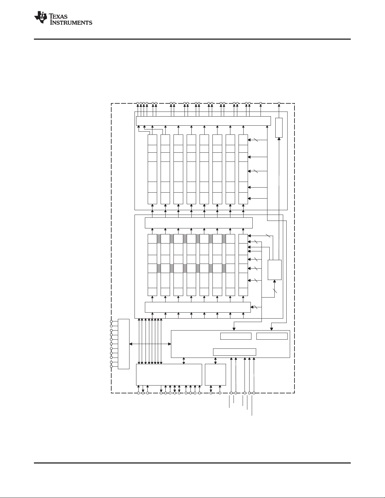
2.2 TAS5508C Functional Description
Figure 2-1 shows the TAS5508C functional structure. The following sections describe the TAS5508C
functional blocks:
• Power supply
Copyright © 2010, Texas Instruments Incorporated Description 17
Submit Documentation Feedback
Product Folder Link(s): TAS5508C
Page 18

TAS5508C
SLES257–SEPTEMBER 2010
• Clock, PLL, and serial data interface
• I2C serial-control interface
• Device control
• Digital audio processor (DAP)
2.2.1 Power Supply
The power-supply section contains supply regulators that provide analog and digital regulated power for
various sections of the TAS5508C. The analog supply supports the analog PLL, whereas digital supplies
support the digital PLL, the digital audio processor (DAP), the pulse-width modulator (PWM), and the
output control (reclocker). The regulators can also be turned off when terminals RESET and PDN are both
low.
2.2.2 Clock, PLL, and Serial Data Interface
The TAS5508C is a clocked slave-only device that requires the use of an external 13.5-MHz crystal. It
accepts MCLK, SCLK, and LRCLK as inputs only.
The TAS5508C uses the external crystal to provide a time base for:
• Continuous data and clock error detection and management
• Automatic data-rate detection and configuration
• Automatic MCLK-rate detection and configuration (automatic bank switching)
• Supporting I2C operation/communication while MCLK is absent
The TAS5508C automatically handles clock errors, data-rate changes, and master-clock frequency
changes without requiring intervention from an external system controller. This feature significantly
reduces system complexity and design.
www.ti.com
2.2.2.1 Serial Audio Interface
The TAS5508C operates as a slave-only/receive-only serial data interface in all modes. The TAS5508C
has four PCM serial data interfaces to permit eight channels of digital data to be received though the
SDIN1, SDIN2, SDIN3, and SDIN4 inputs. The serial audio data is in MSB-first, 2s-complement format.
The serial data input interface of the TAS5508C can be configured in right-justified, I2S, or left-justified
modes. The serial data interface format is specified using the I2C data-interface control register. The
supported formats and word lengths are shown in Table 2-1.
18 Description Copyright © 2010, Texas Instruments Incorporated
Submit Documentation Feedback
Product Folder Link(s): TAS5508C
Page 19
TAS5508C
www.ti.com
RECEIVE SERIAL DATA FORMAT WORD LENGTH
Serial data is input on SDIN1, SDIN2, SDIN3, and SDIN4. The TAS5508C accepts 16-, 20-, or 24-bit
serial data at 32, 38, 44.1, 48, 88.2, 96, 176.4, or 192 kHz in left-justified, I2S, or right-justified format.
Data is input using a 64-Fs SCLK clock and an MCLK rate of 128, 192, 256, 384, 512, or 768 Fs, up to a
maximum of 50 MHz. The clock speed and serial data format are I2C configurable.
2.2.3 I2C Serial-Control Interface
The TAS5508C has an I2C serial-control slave interface (address 0x36) to receive commands from a
system controller. The serial-control interface supports both normal-speed (100 kHz) and high-speed (400
kHz) operations without wait states. Because the TAS5508C has a crystal time base, this interface
operates even when MCLK is absent.
SLES257–SEPTEMBER 2010
Table 2-1. Serial Data Formats
Right-justified 16
Right-justified 20
Right-justified 24
I2S 16
I2S 20
I2S 24
Left-justified 16
Left-justified 20
Left-justified 24
The serial control interface supports both single-byte and multiple-byte read/write operations for status
registers and the general control registers associated with the PWM. However, for the DAP
data-processing registers, the serial control interface also supports multiple-byte (4-byte) write operations.
The I2C supports a special mode which permits I2C write operations to be broken up into multiple
data-write operations that are multiples of 4 data bytes. These are 6-byte, 10-byte, 14-byte, 18-byte, etc.,
write operations that are composed of a device address, read/write bit, subaddress, and any multiple of 4
bytes of data. This permits the system to incrementally write large register values without blocking other
I2C transactions. In order to use this feature, the first block of data is written to the target I2C address, and
each subsequent block of data is written to a special append register (0xFE) until all the data is written
and a stop bit is sent. An incremental read operation is not supported.
2.2.4 Device Control
The TAS5508C control section provides the control and sequencing for the TAS5508C. The device control
provides both high- and low-level control for the serial control interface, clock and serial data interfaces,
digital audio processor, and pulse-width modulator sections.
2.2.5 Digital Audio Processor (DAP)
The DAP arithmetic unit is used to implement all audio-processing functions: soft volume, loudness
compensation, bass and treble processing, dynamic range control, channel filtering, input and output
mixing. Figure 2-3 shows the TAS5508C DAP architecture.
The DAP accepts 24-bit data from the serial data interface and outputs 32-bit data to the PWM section.
The DAP supports two configurations, one for 32-kHz to 96-kHz data and one for 176.4-kHz to 192-kHz
data.
2.2.5.1 TAS5508C Audio-Processing Configurations
The 32-kHz to 96-kHz configuration supports eight channels of data processing that can be configured
either as eight channels, or as six channels with two channels for separate stereo line outputs.
Copyright © 2010, Texas Instruments Incorporated Description 19
Submit Documentation Feedback
Product Folder Link(s): TAS5508C
Page 20

TAS5508C
SLES257–SEPTEMBER 2010
The 176.4-kHz to 192-kHz configuration supports three channels of signal processing with five channels
passed though (or derived from the three processed channels).
To support efficiently the processing requirements of both multichannel 32-kHz to 96-kHz data and the
2-channel 176.4-kHz and 192-kHz data, the TAS5508C has separate audio-processing features for
32-kHz to 96-kHz data rates and for 176.4 kHz and 192 kHz. See Table 2-2 for a summary of TAS5508C
processing feature sets.
2.2.5.2 TAS5508C Audio Signal-Processing Functions
The DAP provides 10 primary signal-processing functions:
1. The data-processing input has a full 8×8 input crossbar mixer. This enables each input to be any ratio
of the eight input channels.
2. Two I2C programmable threshold detectors in each channel support automute.
3. Seven biquads per channel
4. Four soft bass and treble tone controls with ±18-dB range, programmable corner frequencies, and
second-order slopes. In 8-channel mode, bass and treble controls are normally configured as follows:
– Bass and treble 1: Channel 1 (left), channel 2 (right), and channel 7 (center)
– Bass and treble 2: Channel 3 (left surround) and channel 4 (right surround)
– Bass and treble 3: Channel 5 (left back surround) and channel 6 (right back surround)
– Bass and treble 4: Channel 8 (subwoofer)
5. Individual channel and master volume controls. Each control provides an adjustment range of 18 dB to
–127 dB. This permits a total volume device control range of 36 dB to –127 dB plus mute. The master
volume control can be configured to control six or eight channels. The DAP soft volume and mute
update interval is I2C programmable. The update is performed at a fixed rate regardless of the sample
rate.
6. Programmable loudness compensation that is controlled via the combination of the master and
individual volume settings.
7. Two dual-threshold dual-rate dynamic range compressors (DRCs). The volume gain values provided
are used as input parameters using the maximum RMS (master volume × individual channel volume).
8. 8×2 output mixer (channels 1–6). Each output can be any ratio of any two signal-processed channels.
9. 8×3 output mixer (channels 7 and 8). Each output can be any ratio of any three signal-processed
channels.
10. The DAP maintains three sets of coefficient banks that are used to maintain separate sets of
sample-rate-dependent parameters for the biquad, tone controls, loudness, and DRC in RAM. These
can be set to be automatically selected for one or more data sample rates or can be manually selected
under I2C program control. This feature enables coefficients for different sample rates to be stored in
the TAS5508C and then selected when needed.
www.ti.com
20 Description Copyright © 2010, Texas Instruments Incorporated
Submit Documentation Feedback
Product Folder Link(s): TAS5508C
Page 21
TAS5508C
www.ti.com
SLES257–SEPTEMBER 2010
Table 2-2. TAS5508C Audio Processing Feature Sets
FEATURE
Signal-processing channels 8 6 + 2 3
Pass-through channels N/A 5
Master volume 1 for 8 channels 1 for 6 channels 1 for 3 channels
Individual channel volume
controls
Four bass and treble tone controls Four bass and treble tone controls
with ±18-dB range, programmable with ±18-dB range, programmable
Bass and treble tone order slopes order slopes
controls L, R, and C (Ch1, 2, and 7) L, R, and C (Ch1, 2, and 7)
Biquads 56 21
Dynamic range DRC1 for seven satellites and DRC1 for five satellites and DRC2 DRC1 for two satellites and
compressors DRC2 for sub for sub (Ch5 and 6 uncompressed) DRC2 for sub
Input/output mapping/
mixing
DC-blocking filters
(implemented in PWM Eight channels
section)
Digital de-emphasis
(implemented in PWM N/A
section)
Loudness Eight channels Six channels Three channels
Number of coefficient sets
stored
corner frequencies, and second- corner frequencies, and second-
LS, RS (Ch3 and 4) LS, RS (Ch3 and 4)
LBS, RBS (Ch5 and 6) Sub (Ch8)
Sub (Ch8) Line L and R (Ch5 and 6)
Each of the eight signal-processing channel inputs can be any ratio of the be any ratio of the eight input
eight input channels. channels.
Each of the eight outputs can be any ratio of any two processed channels. Each of the eight outputs can be
Eight channels for 32 kHz, Six channels for 32 kHz, 44.1 kHz,
44.1 kHz, and 48 kHz and 48 kHz
32 kHz–96 kHz 32 kHz–96 kHz 176.4- and 192-kHz
8-CHANNEL FEATURE SET 6 + 2 LINEOUT FEATURE SET FEATURE SET
8 3
Two bass and treble tone
controls with ±18-dB range,
programmable corner
frequencies, and second-order
slopes
L and R (Ch1 and 2)
Sub (Ch8)
Each of the three signalprocessing channels or the five
pass-though channel inputs can
any ratio of any of the three
processed channels or five
bypass channels.
Three additional coefficient sets can be stored in memory.
2.3 TAS5508C DAP Architecture
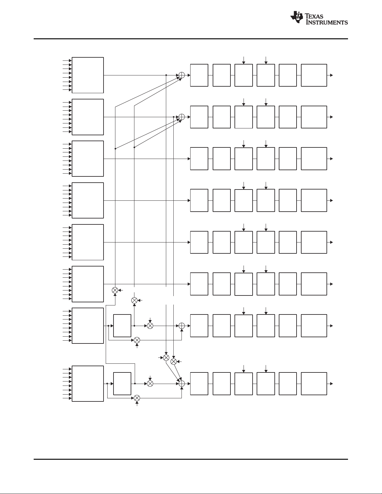
2.3.1 TAS5508C DAP Architecture Diagrams
Figure 2-1 shows the TAS5508C DAP architecture for Fs = 96 kHz. Note the TAS5508C bass
management architecture shown in channels 1, 2, 7, and 8. Note that the I2C registers are shown to help
the designer configure the TAS5508C.
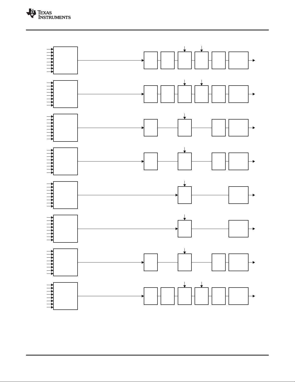
Figure 2-2 shows the TAS5508C architecture for Fs = 176.4 kHz or Fs = 192 kHz. Note that only channels
1, 2, and 8 contain all the features. Channels 3–7 are pass-through except for master volume control.
Figure 2-3 shows TAS5508C detailed channel processing. The output mixer is 8×2 for channels 1–6 and
8×3 for channels 7 and 8.
Copyright © 2010, Texas Instruments Incorporated Description 21
Submit Documentation Feedback
Product Folder Link(s): TAS5508C
Page 22
Coeff = 0 (lin), (I2C 0x4C)
Coeff = 1 (lin)
(I2C 0x4D)
7 DAP 1
BQ
(0x51−
0x57)
SDIN1-L (L)
(1)
SDIN1-R (R)
SDIN2-L (LS)
SDIN2-R (RS)
SDIN3-L (LBS)
SDIN3-R (RBS)
SDIN4-L (C)
SDIN4-R (LFE)
A
B
C
D
E
F
G
H
IP Mixer 1
(I2C 0x41)
8 × 8
Crossbar
Input Mixer
Master Vol
(0xD9)
DAP 1
Volume
(0xD1)
Max Vol
Bass and
Treble 1
(0xDA−
0xDD)
Loud-
ness
(0x91−
0x95)
OP Mixer 1
(I2C 0xAA)
8 × 2 Output
Mixer
L to
PWM1
DRC1
(0x96−
0x9C)
7 DAP 2
BQ
(0x58−
0x5E)
SDIN1-L (L)
SDIN1-R (R)
(1)
SDIN2-L (LS)
SDIN2-R (RS)
SDIN3-L (LBS)
SDIN3-R (RBS)
SDIN4-L (C)
SDIN4-R (LFE)
A
B
C
D
E
F
G
H
IP Mixer 2
(I2C 0x42)
8 × 8
Crossbar
Input Mixer
Master Vol
(0xD9)
DAP 2
Volume
(0xD2)
Max Vol
Bass and
Treble 1
(0xDA−
0xDD)
Loud-
ness
(0x91−
0x95)
OP Mixer 2
(I2C 0xAB)
8 × 2 Output
Mixer
R to
PWM2
DRC1
(0x96−
0x9C)
7 DAP 3
BQ
(0x5F−
0x65)
SDIN1-L (L)
SDIN1-R (R)
SDIN2-L (LS)
(1)
SDIN2-R (RS)
SDIN3-L (LBS)
SDIN3-R (RBS)
SDIN4-L (C)
SDIN4-R (LFE)
A
B
C
D
E
F
G
H
IP Mixer 3
(I2C 0x43)
8 × 8
Crossbar
Input Mixer
Master Vol
(0xD9)
DAP 3
Volume
(0xD3)
Max Vol
Bass and
Treble 2
(0xDA−
0xDD)
Loud-
ness
(0x91−
0x95)
OP Mixer 3
(I2C 0xAC)
8 × 2 Output
Mixer
LS to
PWM3
DRC1
(0x96−
0x9C)
7 DAP 4
BQ
(0x66−
0x6C)
SDIN1-L (L)
SDIN1-R (R)
SDIN2-L (LS)
SDIN2-R (RS)
(1)
SDIN3-L (LBS)
SDIN3-R (RBS)
SDIN4-L (C)
SDIN4-R (LFE)
A
B
C
D
E
F
G
H
IP Mixer 4
(I2C 0x44)
8 × 8
Crossbar
Input Mixer
Master Vol
(0xD9)
DAP 4
Volume
(0xD4)
Max Vol
Bass and
Treble 2
(0xDA−
0xDD)
Loud-
ness
(0x91−
0x95)
OP Mixer 4
(I2C 0xAD)
8 × 2 Output
Mixer
RS to
PWM4
DRC1
(0x96−
0x9C)
7 DAP 5
BQ
(0x6D−
0x73)
SDIN1-L (L)
SDIN1-R (R)
SDIN2-L (LS)
SDIN2-R (RS)
SDIN3-L (LBS)
(1)
SDIN3-R (RBS)
SDIN4-L (C)
SDIN4-R (LFE)
A
B
C
D
E
F
G
H
IP Mixer 5
(I2C 0x45)
8 × 8
Crossbar
Input Mixer
Master Vol
(0xD9)
DAP 5
Volume
(0xD5)
Max Vol
Bass and
Treble 3
(0xDA−
0xDD)
Loud-
ness
(0x91−
0x95)
OP Mixer 5
(I2C 0xAE)
8 × 2 Output
Mixer
LBS to
PWM5
DRC1
(0x96−
0x9C)
7 DAP 6
BQ
(0x74−
0x7A)
SDIN1-L (L)
SDIN1-R (R)
SDIN2-L (LS)
SDIN2-R (RS)
SDIN3-L (LBS)
SDIN3-R (RBS)
(1)
SDIN4-L (C)
SDIN4-R (LFE)
A
B
C
D
E
F
G
H
IP Mixer 6
(I2C 0x46)
8 × 8
Crossbar
Input Mixer
Master Vol
(0xD9)
DAP 6
Volume
(0xD6)
Max Vol
Bass and
Treble 3
(0xDA−
0xDD)
Loud-
ness
(0x91−
0x95)
OP Mixer 6
(I2C 0xAF)
8 × 2 Output
Mixer
RBS to
PWM6
DRC1
(0x96−
0x9C)
5 DAP 7
BQ
(0x7D−
0x81)
SDIN1-L (L)
SDIN1-R (R)
SDIN2-L (LS)
SDIN2-R (RS)
SDIN3-L (LBS)
SDIN3-R (RBS)
SDIN4-L (C)
(1)
SDIN4-R (LFE)
A
B
C
D
E
F
G
H
IP Mixer 7
(I2C 0x47)
8 × 8
Crossbar
Input Mixer
Master Vol
(0xD9)
DAP 7
Volume
(0xD7)
Max Vol
Bass and
Treble 1
(0xDA−
0xDD)
Loud-
ness
(0x91−
0x95)
OP Mixer 7
(I2C 0xB0)
8 × 3 Output
Mixer
C to
PWM7
DRC1
(0x96−
0x9C)
5 DAP 8
BQ
(0x84−
0x88)
SDIN1-L (L)
SDIN1-R (R)
SDIN2-L (LS)
SDIN2-R (RS)
SDIN3-L (LBS)
SDIN3-R (RBS)
SDIN4-L (C)
SDIN4-R (LFE)
(1)
A
B
C
D
E
F
G
H
IP Mixer 8
(I2C 0x48)
8 × 8
Crossbar
Input Mixer
Master Vol
(0xD9)
DAP 8
Volume
(0xD8)
Max Vol
Bass and
Treble 4
(0xDA−
0xDD)
Loud-
ness
(0x91−
0x95)
OP Mixer 8
(I2C 0xB1)
8 × 3 Output
Mixer
Sub to
PWM8
DRC2
(0x9D−
0xA1)
2 DAP 8
BQ
(0x82−
0x83)
B0014-01
Coeff = 0 (lin), (I2C 0x4F)
Coeff = 1 (lin)
(I2C 0x50)
Coeff = 0 (lin), (I2C 0x49)
Coeff = 0 (lin)
(I2C 0x4A)
2 DAP 7
BQ
(0x7B−
0x7C)
Coeff = 0 (lin), (I2C 0x4B)
Coeff = 0 (lin), (I2C 0x4E)
TAS5508C
SLES257–SEPTEMBER 2010
www.ti.com
(1) Default inputs
Figure 2-1. TAS5508C DAP Architecture With I2C Registers (Fs ≤ 96 kHz)
22 Description Copyright © 2010, Texas Instruments Incorporated
Submit Documentation Feedback
Product Folder Link(s): TAS5508C
Page 23
B0015-03
SDIN1-L (L)
(1)
SDIN1-L (L)
SDIN1-L (L)
SDIN1-L (L)
SDIN1-L (L)
SDIN1-L (L)
SDIN1-L (L)
SDIN1-L (L)
SDIN1-R (R)
SDIN1-R (R)
(1)
SDIN1-R (R)
SDIN1-R (R)
SDIN1-R (R)
SDIN1-R (R)
SDIN1-R (R)
SDIN1-R (R)
SDIN2-L (LS)
SDIN2-L (LS)
SDIN2-L (LS)
(1)
SDIN2-L (LS)
SDIN2-L (LS)
SDIN2-L (LS)
SDIN2-L (LS)
SDIN2-L (LS)
SDIN2-R (RS)
SDIN2-R (RS)
SDIN2-R (RS)
SDIN2-R (RS)
(1)
SDIN2-R (RS)
SDIN2-R (RS)
SDIN2-R (RS)
SDIN2-R (RS)
SDIN3-L (LBS)
SDIN3-L (LBS)
SDIN3-L (LBS)
SDIN3-L (LBS)
SDIN3-L (LBS)
(1)
SDIN3-L (LBS)
SDIN3-L (LBS)
SDIN3-L (LBS)
SDIN3-R (RBS)
SDIN3-R (RBS)
SDIN3-R (RBS)
SDIN3-R (RBS)
SDIN3-R (RBS)
SDIN3-R (RBS)
(1)
SDIN3-R (RBS)
SDIN3-R (RBS)
SDIN4-L (C)
SDIN4-L (C)
SDIN4-L (C)
SDIN4-L (C)
SDIN4-L (C)
SDIN4-L (C)
SDIN4-L (C)
(1)
SDIN4-L (C)
SDIN4-R (LFE)
SDIN4-R (LFE)
SDIN4-R (LFE)
SDIN4-R (LFE)
SDIN4-R (LFE)
SDIN4-R (LFE)
SDIN4-R (LFE)
SDIN4-R (LFE)
(1)
A
A
A
A
A
A
A
A
B
B
B
B
B
B
B
B
C
C
C
C
C
C
C
C
D
D
D
D
D
D
D
D
E
E
E
E
E
E
E
E
F
F
F
F
F
F
F
F
G
G
G
G
G
G
G
G
H
H
H
H
H
H
H
H
Max Vol
Max Vol
Max Vol
IP Mixer 1
(I C 0x41)
8 8
Crossbar
Input Mixer
2
´
IP Mixer 2
(I C 0x42)
8 8
Crossbar
Input Mixer
2
´
IP Mixer 3
(I C 0x43)
8 8
Crossbar
Input Mixer
2
´
IP Mixer 4
(I C 0x44)
8 8
Crossbar
Input Mixer
2
´
IP Mixer 5
(I C 0x45)
8 8
Crossbar
Input Mixer
2
´
IP Mixer 6
(I C 0x46)
8 8
Crossbar
Input Mixer
2
´
IP Mixer 7
(I C 0x47)
8 8
Crossbar
Input Mixer
2
´
IP Mixer 8
(I C 0x48)
8 8
Crossbar
Input Mixer
2
´
OP Mixer 1
(I C 0xAA)
8 2
Output Mixer
2
´
OP Mixer 2
(I C 0xAB)
8 2
Output Mixer
2
´
OP Mixer 3
(I C 0xAC)
8 2
Output Mixer
2
´
OP Mixer 4
(I C 0xAD)
8 2
Output Mixer
2
´
OP Mixer 5
(I C 0xAE)
8 2
Output Mixer
2
´
OP Mixer 6
(I C 0xAF)
8 2
Output Mixer
2
´
OP Mixer 7
(I C 0xB0)
8 3
Output Mixer
2
´
OP Mixer 8
(I C 0xB1)
8 3
Output Mixer
2
´
Master Vol
(0xD9)
Master Vol
(0xD9)
Master Vol
(0xD9)
Master Vol
(0xD9)
Master Vol
(0xD9)
Master Vol
(0xD9)
Master Vol
(0xD9)
Master Vol
(0xD9)
4BQ
(0x51–
0x54)
4BQ
(0x58–
0x5B)
3BQ
(0x5F–
0x61)
3BQ
(0x66–
0x68)
3BQ
(0x7B–
0x7D)
4BQ
(0x82–
0x85)
Loud-
ness
(0x91–
0x95)
Loud-
ness
(0x91–
0x95)
Loud-
ness
(0x91–
0x95)
DRC1
(0x96–
0x9C)
DRC1
(0x96–
0x9C)
DRC1
(0x96–
0x9C)
DRC1
(0x96–
0x9C)
DRC2
(0x9D–
0xA1)
DRC1
(0x96–
0x9C)
DAP 1
Volume
(0xD1)
DAP 2
Volume
(0xD2)
DAP 3
Volume
(0xD3)
DAP 4
Volume
(0xD4)
DAP 5
Volume
(0xD5)
DAP 6
Volume
(0xD6)
DAP 7
Volume
(0xD7)
DAP 8
Volume
(0xD8)
L to
PWM1
R to
PWM2
LS to
PWM3
RS to
PWM4
LBS to
PWM5
RBS to
PWM6
C to
PWM7
Sub to
PWM8
Bass
Treble 1
(0xDA–
0xDD)
and
Bass
Treble 1
(0xDA–
0xDD)
and
Bass
Treble 4
(0xDA–
0xDD)
and
TAS5508C
www.ti.com
(1) Default inputs
Figure 2-2. TAS5508C Architecture With I2C Registers (Fs = 176.4 kHz or Fs = 192 kHz)
Copyright © 2010, Texas Instruments Incorporated Description 23
Submit Documentation Feedback
Product Folder Link(s): TAS5508C
SLES257–SEPTEMBER 2010
Page 24
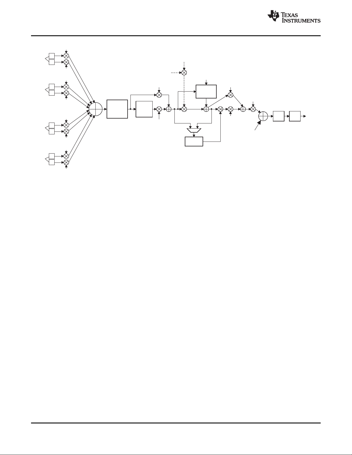
7
Biquads
in
Series
Bass
and
Treble
Loudness
DRC
Input
Mixer
1 Other
Channel Output
From 7 Available
32-Bit
Trunc
PWM
Proc
A_to_ipmix
B_to_ipmix
A
SDIN1
B
C_to_ipmix
D_to_ipmix
SDIN2
Left
Right
Channel Volume
Bass and Treble
Bypass
Bass
and
Treble
Inline
Pre-
Volume
Post-
Volume
Output
Gain
Output Mixer Sums
Any Two Channels
PWM
Output
C
D
Left
Right
DRC
Bypass
DRC
Inline
E_to_ipmix
F_to_ipmix
E
SDIN3
F
G_to_ipmix
H_to_ipmix
SDIN4
Left
Right
G
H
Left
Right
B0016-01
Master
Volume
Max
Volume
TAS5508C
SLES257–SEPTEMBER 2010
www.ti.com
Figure 2-3. TAS5508C Detailed Channel Processing
2.3.2 I2C Coefficient Number Formats
The architecture of the TAS5508C is contained in ROM resources within the TAS5508C and cannot be
altered. However, mixer gain, level offset, and filter tap coefficients, which can be entered via the I2C bus
interface, provide a user with the flexibility to set the TAS5508C to a configuration that achieves
system-level goals.
The firmware is executed in a 48-bit, signed, fixed-point arithmetic machine. The most significant bit of the
48-bit data path is a sign bit, and the 47 lower bits are data bits. Mixer gain operations are implemented
by multiplying a 48-bit, signed data value by a 28-bit, signed gain coefficient. The 76-bit, signed output
product is then truncated to a signed, 48-bit number. Level offset operations are implemented by adding a
48-bit, signed offset coefficient to a 48-bit, signed data value. In most cases, if the addition results in
overflowing the 48-bit, signed number format, saturation logic is used. This means that if the summation
results in a positive number that is greater than 0x7FFF FFFF FFFF (the spaces are used to ease the
reading of the hexadecimal number), the number is set to 0x7FFF FFFF FFFF. If the summation results in
a negative number that is less than 0x80000000 0000, the number is set to 0x8000 0000 0000.
2.3.2.1 28-Bit 5.23 Number Format
All mixer gain coefficients are 28-bit coefficients using a 5.23 number format. Numbers formatted as 5.23
numbers have 5 bits to the left of the binary point and 23 bits to the right of the binary point. This is shown
in Figure 2-4.
24 Description Copyright © 2010, Texas Instruments Incorporated
Submit Documentation Feedback
Product Folder Link(s): TAS5508C
Page 25
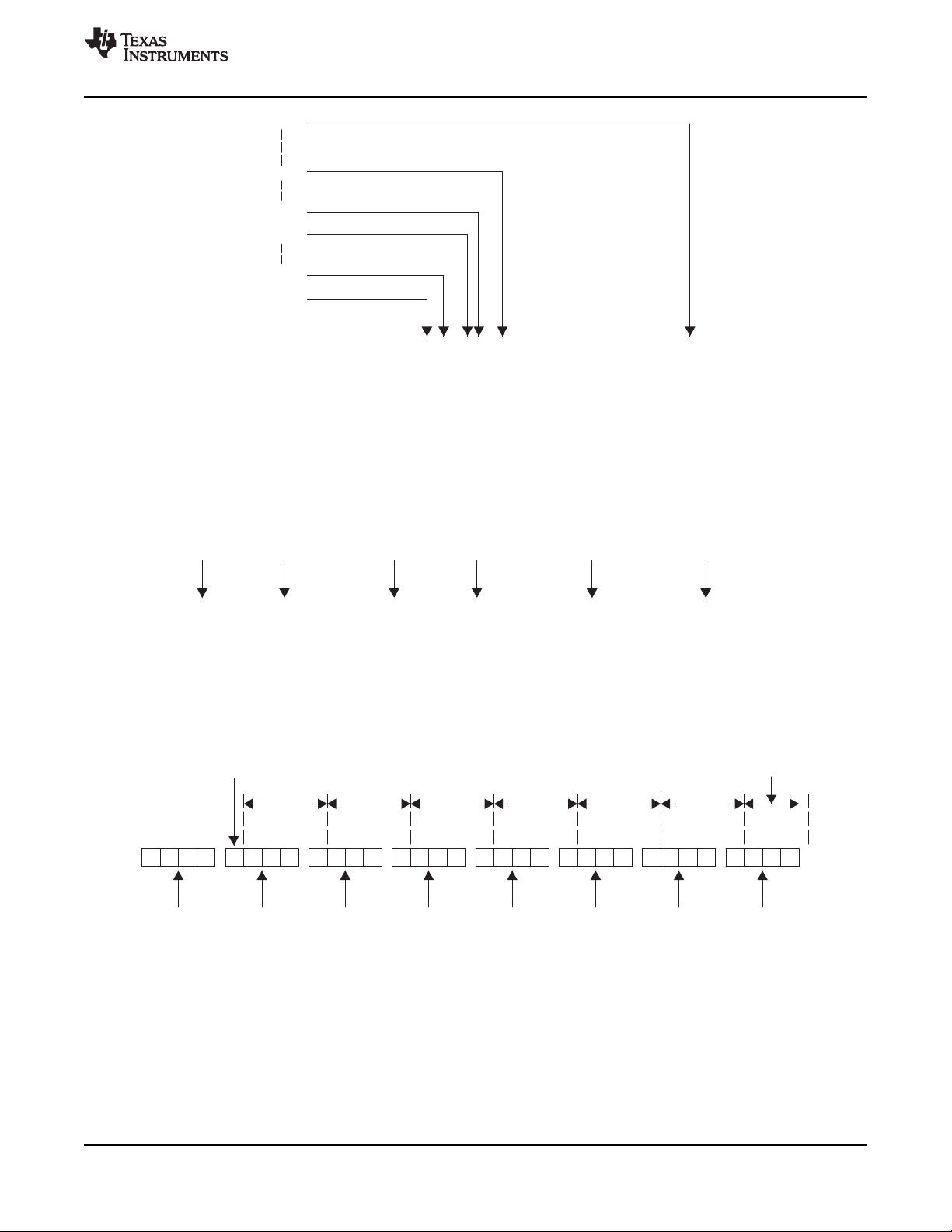
2
−23
Bit
S_xxxx.xxxx_xxxx_xxxx_xxxx_xxxx_xxx
2−4 Bit
2−1 Bit
20 Bit
Sign Bit
23 Bit
M0007-01
(1 or 0) y 23 + (1 or 0) y 22 + … + (1 or 0) y 20 + (1 or 0) y 2−1 + … + (1 or 0) y 2−4 + … + (1 or 0) y 2
−23
23 Bit 22 Bit 20 Bit 2−1 Bit 2−4 Bit 2
−23
Bit
M0008-01
u
Coefficient
Digit 8
u
u u S x x x
Coefficient
Digit 7
x.
x x x
Coefficient
Digit 6
x
x x x
Coefficient
Digit 5
x
x x x
Coefficient
Digit 4
x
x x x
Coefficient
Digit 3
x
x x x
Coefficient
Digit 2
x
x x x
Coefficient
Digit 1
Fraction
Digit 5
Sign
Bit
0
Fraction
Digit 6
Fraction
Digit 4
Fraction
Digit 3
Fraction
Digit 2
Fraction
Digit 1
Integer
Digit 1
u = unused or don’t care bits
Digit = hexadecimal digit
M0009-01
TAS5508C
www.ti.com
The decimal value of a 5.23 format number can be found by following the weighting shown in Figure 2-5. If
the most significant bit is logic 0, the number is a positive number, and the weighting shown yields the
correct number. If the most significant bit is a logic 1, then the number is a negative number. In this case,
every bit must be inverted, a 1 added to the result, and then the weighting shown in Figure 2-5 applied to
obtain the magnitude of the negative number.
SLES257–SEPTEMBER 2010
Figure 2-4. 5.23 Format
Figure 2-5. Conversion Weighting Factors—5.23 Format to Floating Point
Gain coefficients, entered via the I2C bus, must be entered as 32-bit binary numbers. The format of the
32-bit number (4-byte or 8-digit hexadecimal number) is shown in Figure 2-6.
Figure 2-6. Alignment of 5.23 Coefficient in 32-Bit I2C Word
As Figure 2-6 shows, the hexadecimal (hex) value of the integer part of the gain coefficient cannot be
Copyright © 2010, Texas Instruments Incorporated Description 25
Submit Documentation Feedback
Product Folder Link(s): TAS5508C
Page 26
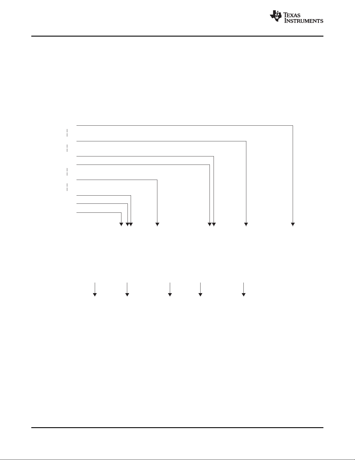
2
−23
Bit
S_xxxx_xxxx_xxxx_xxxx_xxxx_xxxx.xxxx_xxxx_xxxx_xxxx_xxxx_xxx
20 Bit
216 Bit
222 Bit
Sign Bit
223 Bit
2−1 Bit
2
−10
Bit
M0007-02
(1 or 0) y 223 + (1 or 0) y 222 + … + (1 or 0) y 20 + (1 or 0) y 2−1 + … + (1 or 0) y 2
−23
223 Bit 222 Bit 20 Bit 2−1 Bit 2
−23
Bit
M0008-02
TAS5508C
SLES257–SEPTEMBER 2010
concatenated with the hex value of the fractional part of the gain coefficient to form the 32-bit I2C
coefficient. The reason is that the 28-bit coefficient contains 5 bits of integer, and thus the integer part of
the coefficient occupies all of one hex digit and the most significant bit of the second hex digit. In the same
way, the fractional part occupies the lower three bits of the second hex digit, and then occupies the other
five hex digits (with the eighth digit being the zero-valued most significant hex digit).
2.3.2.2 48-Bit 25.23 Number Format
All level adjustment and threshold coefficients are 48-bit coefficients using a 25.23 number format.
Numbers formatted as 25.23 numbers have 25 bits to the left of the decimal point and 23 bits to the right
of the decimal point. This is shown in Figure 2-7.
www.ti.com
Figure 2-7. 25.23 Format
Figure 2-8 shows the derivation of the decimal value of a 48-bit 25.23 format number.
Figure 2-8. Alignment of 5.23 Coefficient in 32-Bit I2C Word
Two 32-bit words must be sent over the I2C bus to download a level or threshold coefficient into the
TAS5508C. The alignment of the 48-bit, 25.23 formatted coefficient in the 8-byte (two 32-bit words) I2C
word is shown in Figure 2-9.
26 Description Copyright © 2010, Texas Instruments Incorporated
Submit Documentation Feedback
Product Folder Link(s): TAS5508C
Page 27
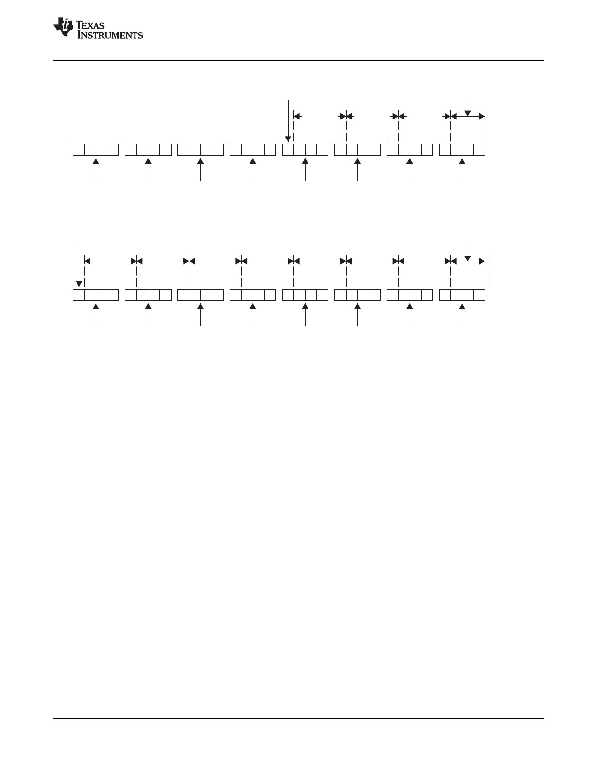
u
Coefficient
Digit 16
u
u u u u u u
Coefficient
Digit 15
u
u u u
Coefficient
Digit 14
u
u u u
Coefficient
Digit 13
S
x x x
Coefficient
Digit 12
x
x x x
Coefficient
Digit 11
x
x x x
Coefficient
Digit 10
x
x x x
Coefficient
Digit 9
Word 1
(MostSignificant
Word)
Integer
Digit 3
Integer
Digit 4
(Bits 211 − 29)
Integer
Digit 2
Integer
Digit 1
Sign
Bit
x
Coefficient
Digit 8
x
x x x x x x
Coefficient
Digit 7
x.
x x x
Coefficient
Digit 6
x
x x x
Coefficient
Digit 5
x
x x x
Coefficient
Digit 4
x
x x x
Coefficient
Digit 3
x
x x x
Coefficient
Digit 2
x
x x x
Coefficient
Digit 1
Word 2
(LeastSignificant
Word)
Fraction
Digit 5
Integer
Digit 4
(Bit 28)
0
Fraction
Digit 6
Fraction
Digit 4
Fraction
Digit 3
Fraction
Digit 2
Fraction
Digit 1
Integer
Digit 6
Integer
Digit 5
u = unused or don’t care bits
Digit = hexadecimal digit
M0009-02
TAS5508C
www.ti.com
SLES257–SEPTEMBER 2010
2.3.2.3 TAS5508C Audio Processing
Figure 2-9. Alignment of 25.23 Coefficient in Two 32-Bit I2C Words
The TAS5508C digital audio processing is designed so that noise produced by filter operations is
maintained below the smallest signal amplitude of interest, as shown in Figure 2-10. The TAS5508C
achieves this low noise level by increasing the precision of the signal representation substantially above
the number of bits that are absolutely necessary to represent the input signal.
Similarly, the TAS5508C carries additional precision in the form of overflow bits to permit the value of
intermediate calculations to exceed the input precision without clipping. The TAS5508C advanced digital
audio processor achieves both of these important performance capabilities by using a high-performance
digital audio processing architecture with a 48-bit data path, 28-bit filter coefficients, and a 76-bit
accumulator.
Copyright © 2010, Texas Instruments Incorporated Description 27
Submit Documentation Feedback
Product Folder Link(s): TAS5508C
Page 28
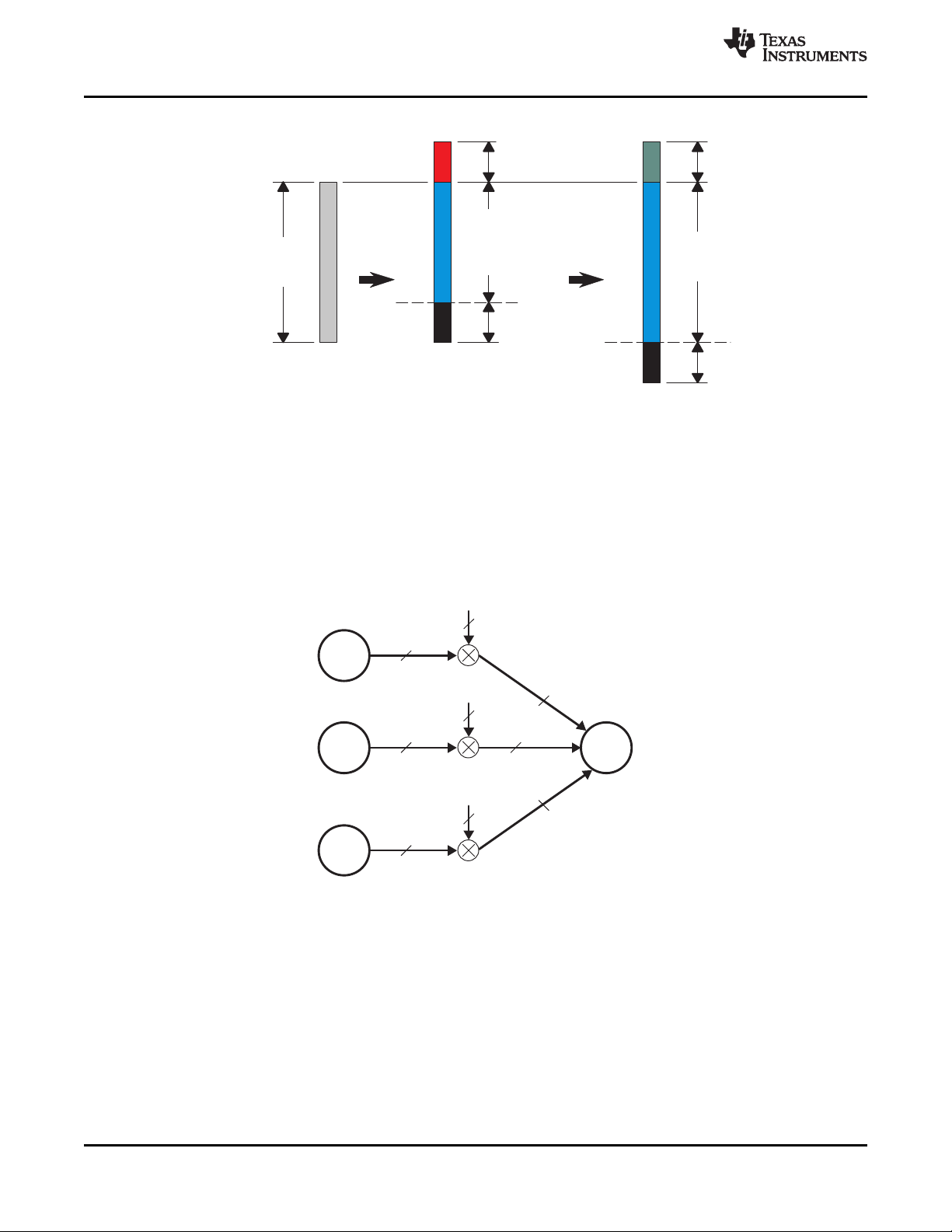
Noise Floor With No
Additional Precision
Maximum Signal Amplitude
Ideal Input Possible Outputs Desired Output
Filter
Operation
Signal
Bits
Input
Overflow
Reduced
SNR
Signal
Output
Noise Floor as a Result
of Additional Precision
Signal
Bits
Output
Values Retained by
Overflow Bits
M0010-01
Gain Coefficient
48
SDIN1-L
28
48
Gain Coefficient
48
28
48
SUM
w
w
w
Gain Coefficient
48
28
48
M0011-01
SDIN1-R
SDIN4-R
TAS5508C
SLES257–SEPTEMBER 2010
2.4 Input Crossbar Mixer
The TAS5508C has a full 8×8 input crossbar mixer. This mixer permits each signal processing channel
input to be any ratio of any of the eight input channels, as shown in Figure 2-11. The control parameters
for the input crossbar mixer are programmable via the I2C interface. See the Input Mixer Registers
(0x41–0x48, Channels 1–8), Section 7.16, for more information.
www.ti.com
Figure 2-10. TAS5508C Digital Audio Processing
2.5 Biquad Filters
For 32-kHz to 96-kHz data, the TAS5508C provides 56 biquads across the eight channels (seven per
channel).
For 176.4-kHz and 192-kHz data, the TAS5508C has 21 biquads across the three channels (seven per
channel). All of the biquad filters are second-order direct form I structure.
28 Description Copyright © 2010, Texas Instruments Incorporated
Figure 2-11. Input Crossbar Mixer
Submit Documentation Feedback
Product Folder Link(s): TAS5508C
Page 29
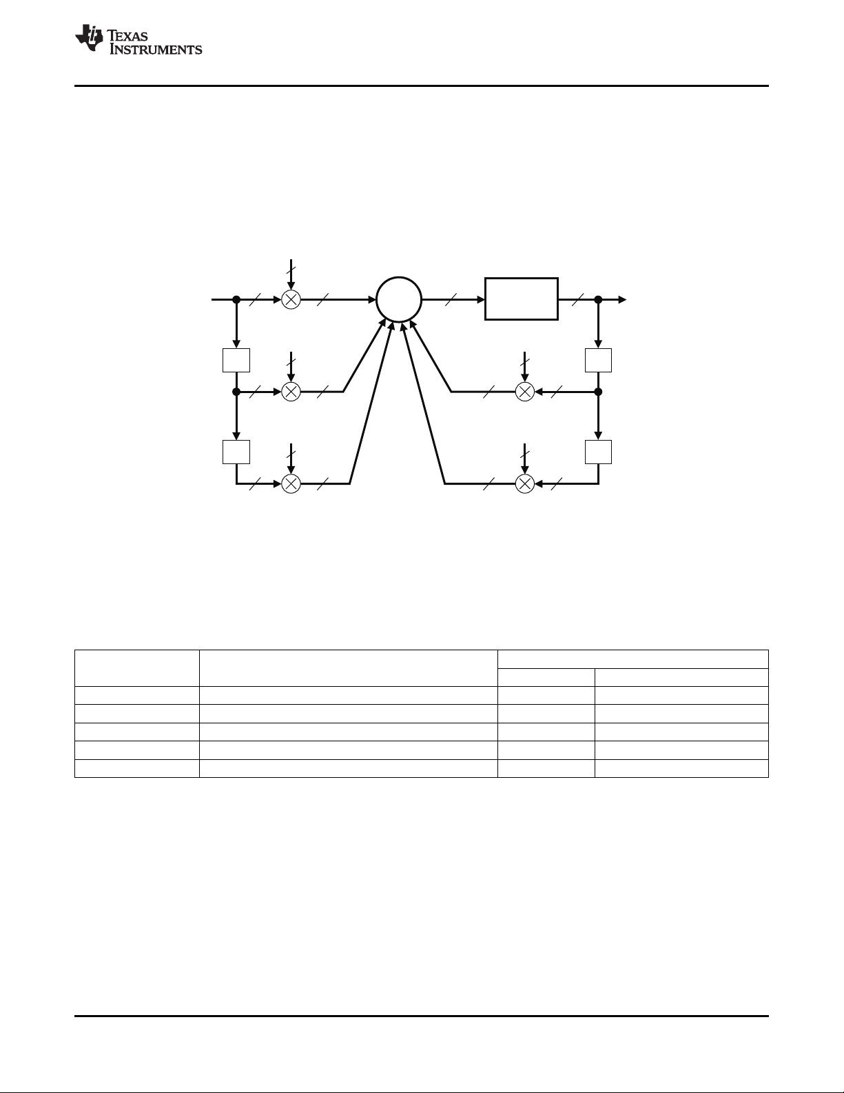
28
48 76 48
b
0
28
48 76
b
1
S
28
48 76
b
2
76
28
76 48
a
1
28
76 48
a
2
M0012-01
z
–1
z
–1
Magnitude
Truncation
z
–1
z
–1
TAS5508C
www.ti.com
The direct form I structure provides a separate delay element and mixer (gain coefficient) for each node in
the biquad filter. Each mixer output is a signed 76-bit product of a signed 48-bit data sample (25.23 format
number) and a signed 28-bit coefficient (5.23 format number), as shown in Figure 2-12. The 76-bit ALU in
the TAS5508C allows the 76-bit resolution to be retained when summing the mixer outputs (filter
products).
The five 28-bit coefficients for the each of the 56 biquads are programmable via the I2C interface. See
Table 2-3.
SLES257–SEPTEMBER 2010
Figure 2-12. Biquad Filter Structure
All five coefficients for one biquad filter structure are written to one I2C register containing 20 bytes (or five
32-bit words). The structure is the same for all biquads in the TAS5508C. Registers 0x51–0x88 show all
the biquads in the TAS5508C. Note that u[31:28] bits are unused and default to 0x0.
Table 2-3. Contents of One 20-Byte Biquad Filter Register (Default = All-Pass)
DESCRIPTION REGISTER FIELD CONTENTS
b0coefficient u[31:28], b0[27:24], b0[23:16], b0[15:8], b0[7:0] 1.0 0x00, 0x80, 0x00, 0x00
b1coefficient u[31:28], b1[27:24], b1[23:16], b1[15:8], b1[7:0] 0.0 0x00, 0x00, 0x00, 0x00
b2coefficient u[31:28], b2[27:24], b2[23:16], b2[15:8], b2[7:0] 0.0 0x00, 0x00, 0x00, 0x00
a1coefficient u[31:28], a1[27:24], a1[23:16], a1[15:8], a1[7:0] 0.0 0x00, 0x00, 0x00, 0x00
a2coefficient u[31:28], a2[27:24], a2[23:16], a2[15:8], a2[7:0] 0.0 0x00, 0x00, 0x00, 0x00
2.6 Bass and Treble Controls
From 32-kHz to 96-kHz data, the TAS5508C has four bass and treble tone controls. Each control has a
±18-dB control range with selectable corner frequencies and second-order slopes. These controls operate
four channel groups:
• L, R, and C (channels 1, 2, and 7)
• LS, RS (channels 3 and 4)
• LBS, RBS (alternatively called L and R lineout) (channels 5 and 6)
• Sub (channel 8)
For 176.4-kHz and 192-kHz data, the TAS5508C has two bass and treble tone controls. Each control has
a ±18-dB I2C control range with selectable corner frequencies and second-order slopes. These controls
operate two channel groups:
Copyright © 2010, Texas Instruments Incorporated Description 29
Submit Documentation Feedback
Product Folder Link(s): TAS5508C
INITIALIZATION GAIN COEFFICIENT VALUE
DECIMAL HEX
Page 30
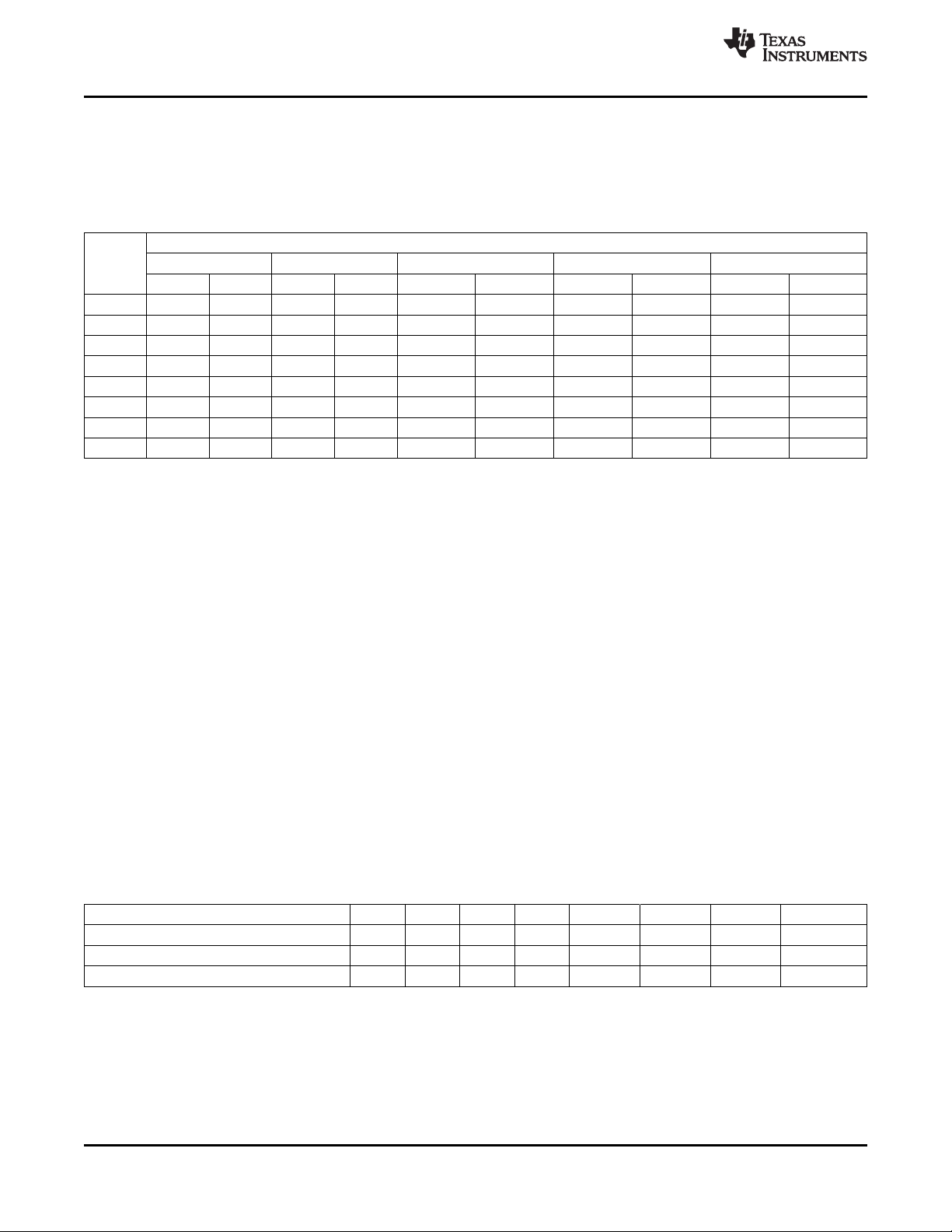
TAS5508C
SLES257–SEPTEMBER 2010
www.ti.com
• L and R
• Sub
The bass and treble filters use a soft update rate that does not produce artifacts during adjustment.
Table 2-4. Bass and Treble Filter Selections
FS
(kHz)
32 42 917 83 1833 125 3000 146 3667 167 4333
38 49 1088 99 2177 148 3562 173 4354 198 5146
44.1 57 1263 115 2527 172 4134 201 5053 230 5972
48 63 1375 125 2750 188 4500 219 5500 250 6500
88.2 115 2527 230 5053 345 8269 402 10106 459 11944
96 125 2750 250 5500 375 9000 438 11000 500 13000
176.4 230 5053 459 10106 689 16538 804 20213 919 23888
192 250 5500 500 11000 750 18000 875 22000 1000 26000
FILTER SET 1 FILTER SET 2 FILTER SET 3 FILTER SET 4 FILTER SET 5
BASS TREBLE BASS TREBLE BASS TREBLE BASS TREBLE BASS TREBLE
3-dB CORNER FREQUENCIES
The I2C registers that control bass and treble are:
• Bass and treble bypass register (0x89–0x90, channels 1–8)
• Bass and treble slew rates (0xD0)
• Bass filter sets 1–5 (0xDA)
• Bass filter index (0xDB)
• Treble filter sets 1–5 (0xDC)
• Treble filter index (0xDD)
2.7 Volume, Automute, and Mute
The TAS5508C provides individual channel and master volume controls. Each control provides an
adjustment range of 18 dB to –100 dB in 0.25-dB increments. This permits a total volume device control
range of 36 dB to –100 dB plus mute. The master volume control can be configured to control six or eight
channels.
The TAS5508C has a master soft mute control that can be enabled by a terminal or I2C command. The
device also has individual channel soft mute controls that are enabled via I2C.
The soft volume and mute update rates are programmable. The soft adjustments are performed using a
soft-gain linear update with an I2C-programmable linear step size at a fixed temporal rate. The linear
soft-gain step size can be varied from 0.5 to 0.003906. Table 2-5 lists the linear gain step sizes.
Table 2-5. Linear Gain Step Size
STEP SIZE (GAIN) 0.5 0.25 0.125 0.0625 0.03125 0.015625 0.007813 0.003906
Time to go from 36.124 db to –127 dB in ms 10.67 21.33 42.67 85.34 170.67 340.35 682.70 1365.4
Time to go from 18.062 db to –127 dB in ms 1.33 2.67 5.33 10.67 21.33 42.67 85.33 170.67
Time to go from 0 db to –127 dB in ms 0.17 0.33 0.67 1.33 2.67 5.33 10.67 21.33
2.8 Automute and Mute
The TAS5508C has individual channel automute controls that are enabled via the I2C interface. Two
separate detectors can trigger the automute:
• Input automute: All channels are muted when all 8 inputs to the TAS5508C are less in magnitude than
the input threshold value for a programmable amount of time.
30 Description Copyright © 2010, Texas Instruments Incorporated
Submit Documentation Feedback
Product Folder Link(s): TAS5508C
Page 31
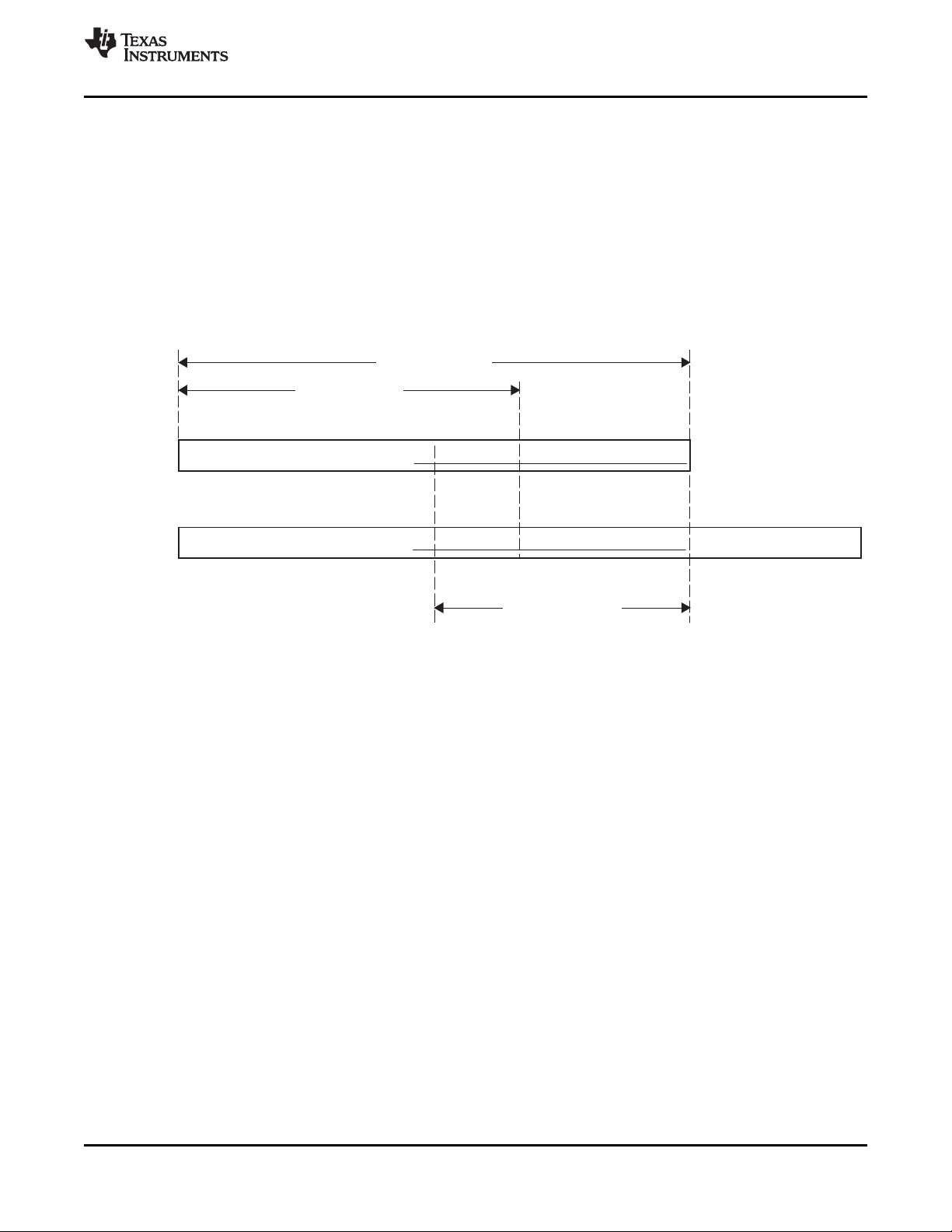
24-Bit Input
32 Bits in DSPE
Representation
31 30 29 28 27 26 25 24 23 22 21 20 19 18 17 16 15 14 13 12 11 10 9 8 7 6 5 4 3 2 1 0
23 22 21 20 19 18 17 16 15 14 13 12 11 10 9 8 7 6 5 4 3 2 1 0
Threshold Range
CD Data Range
DVD Data Range
M0013-01
TAS5508C
www.ti.com
• Output automute: A single channel is muted when the output of the DAP section is less in magnitude
The detection period and thresholds for these two detectors are the same.
This time interval is selectable via I2C to be from 1 ms to 110 ms. The increments of time are 1, 2, 3, 4, 5,
10, 20, 30, 40, 50, 60, 70, 80, 90, 100, and 110 ms. This interval is independent of the sample rate. The
default value is mask programmable.
The input threshold value is an unsigned magnitude that is expressed as a bit position. This value is
adjustable via I2C. The range of the input threshold adjustment is from below the LSB (bit position 0) to
below bit position 12 in a 24-bit input-data word (bit positions 8 to 20 in the DSPE). This range provides an
input threshold that can be adjusted for 12 to 24 bits of data. The default value is mask programmable.
SLES257–SEPTEMBER 2010
than the input threshold value for a programmable amount of time.
Figure 2-13. Automute Threshold
The automute state is exited when the TAS5508C receives one sample that is greater than the output
threshold.
The output threshold can be one of two values:
• Equal to the input threshold
• 6 dB (one bit position) greater than the input threshold
The value for the output threshold is selectable via I2C. The default value is mask programmable.
The system latency enables the data value that is above the threshold to be preserved and output.
A mute command initiated by automute, master mute, individual I2C mute, the AM interference mute
sequence, or the bank-switch mute sequence overrides an unmute command or a volume command.
While a mute command is activated, the commanded channels transition to the mute state. When a
channel is unmuted, it goes to the last commanded volume setting that has been received for that
channel.
2.9 Loudness Compensation
The loudness compensation function compensates for the Fletcher-Munson loudness curves. The
TAS5508C loudness implementation tracks the volume control setting to provide spectral compensation
for weak low- or high-frequency response at low volume levels. For the volume tracking function, both
linear and logarithmic control laws can be implemented. Any biquad filter response can be used to provide
the desired loudness curve. The control parameters for the loudness control are programmable via the I2C
interface.
Copyright © 2010, Texas Instruments Incorporated Description 31
Submit Documentation Feedback
Product Folder Link(s): TAS5508C
Page 32

B0017-01
Loudness
Biquad
H(z)
Audio OutAudio In
V
VLoudness Function = f(V)
TAS5508C
SLES257–SEPTEMBER 2010
The TAS5508C has a single set of loudness controls for the eight channels. In 6-channel mode, loudness
is available to the six speaker outputs and also to the line outputs. The loudness control input uses the
maximum individual master volume (V) to control the loudness that is applied to all channels. In the
192-kHz and 176.4-kHz modes, the loudness function is active only for channels 1, 2, and 8.
Loudness function = f(V) = G ×[2
Loudness function = f(V) = G × [VLG× 2LO] + O
Figure 2-14. Loudness Compensation Functional Block Diagram
(Log V) × LG + LO
] + O or alternatively,
www.ti.com
For example, for the default values LG = –0.5, LO = 0, G = 1, and O = 0, then:
Loudness function = 1/SQRT(V), which is the recommended transfer function for loudness. So,
Audio out = (audio in) × V + H(Z) × SQRT(V). Other transfer functions are possible.
Table 2-6. Default Loudness Compensation Parameters
LOUDNESS DESCRIPTION USAGE DATA I2C DEFAULT
TERM FORMAT SUB-
ADDRESS
V Max volume Gains audio 5.23 NA NA NA
Log V Log2(max volume) Loudness function 5.23 NA 0000 0000 0.0
H(Z) Loudness biquad Controls shape of 5.23 0x95 b0= 0000 D513 b0= 0.006503
loudness curves b1= 0000 0000 b1= 0
LG Gain (log space) Loudness function 5.23 0x91 FFC0 0000 –0.5
LO Offset (log space) Loudness function 25.23 0x92 0000 0000 0
G Gain Switch to enable 5.23 0x93 0000 0000 0
loudness (ON = 1, OFF = 0)
O Offset Provides offset 25.23 0x94 0000 0000 0
HEX FLOAT
b2= 0FFF 2AED b2= –0.006503
a1= 00FE 5045 a1= 1.986825
a2= 0F81 AA27 a2= –0.986995
2.9.1 Loudness Example
Problem: Due to the Fletcher-Munson phenomena, we want to compensate for low-frequency attenuation
near 60 Hz. The TAS5508C provides a loudness transfer function with EQ gain = 6, EQ center frequency
= 60 Hz, and EQ bandwidth = 60 Hz.
Solution: Using Texas Instruments ALE TAS5508C DSP tool, Matlab™, or other signal-processing tool,
develop a loudness function with the parameters listed in Table 2-7.
32 Description Copyright © 2010, Texas Instruments Incorporated
Submit Documentation Feedback
Product Folder Link(s): TAS5508C
Page 33

f − Frequency − Hz
Gain − dB
10 20k100 1k
G001
20
0
−10
−20
−40
10
−30
10k
TAS5508C
www.ti.com
SLES257–SEPTEMBER 2010
Table 2-7. Loudness Function Parameters
LOUDNESS DESCRIPTION USAGE DATA I2C DEFAULT
TERM FORMAT SUB-
ADDRESS
H(Z) Loudness biquad Controls shape of 5.23 0x95 b0= 0000 8ACE b0= 0.004236
Loudness curves b1= 0000 0000 b1= 0
LG Loudness gain Loudness function 5.23 0x91 FFC0 0000 –0.5
LO Loudness offset Loudness function 25.23 0x92 0000 0000 0
G Gain Switch to enable 5.23 0x93 0080 0000 1
loudness (ON = 1, OFF = 0)
O Offset Offset 25.23 0x94 0000 0000 0
HEX FLOAT
b2= FFFF 7532 b2= –0.004236
a1= FF01 1951 a1= –1.991415
a2= 007E E914 a2= 0.991488
See Figure 2-15 for the resulting loudness function at different gains.
2.10 Dynamic Range Control (DRC)
DRC provides both compression and expansion capabilities over three separate and definable regions of
audio signal levels. Programmable threshold levels set the boundaries of the three regions. Within each of
the three regions, a distinct compression or expansion transfer function can be established and the slope
of each transfer function is determined by programmable parameters. The offset (boost or cut) at the two
boundaries defining the three regions can also be set by programmable offset coefficients. The DRC
implements the composite transfer function by computing a 5.23-format gain coefficient from each sample
output from the rms estimator. This gain coefficient is then applied to a mixer element, whose other input
is the audio data stream. The mixer output is the DRC-adjusted audio data.
There are two distinct DRC blocks in the TAS5508C. DRC1 services channels 1–7 in the 8-channel mode
and channels 1–4 and 7 in the 6-channel mode. This DRC computes rms estimates of the audio data
streams on all channels that it controls. The estimates are then compared on a sample-by-sample basis
and the larger of the estimates is used to compute the compression/expansion gain coefficient. The gain
coefficient is then applied to the appropriate channel audio streams. DRC2 services only channel 8. This
DRC also computes an rms estimate of the signal level on channel 8 and this estimate is used to compute
the compression/expansion gain coefficient applied to the channel-8 audio stream.
Copyright © 2010, Texas Instruments Incorporated Description 33
Figure 2-15. Loudness Example Plots
Submit Documentation Feedback
Product Folder Link(s): TAS5508C
Page 34

7
Biquads
in
Series
Bass
and
Treble
DRC
Bass and Treble
Bypass
Bass
and
Treble
Inline
Pre-
Volume
Post-
Volume
DRC
Bypass
DRC
Inline
B0016-02
From Input Mixer To Output Mixer
Loudness
Channel Volume
Master
Volume
Max
Volume
TAS5508C
SLES257–SEPTEMBER 2010
All of the TAS5508C default values for DRC can be used except for the DRC1 decay and DRC2 decay.
Table 2-8 shows the recommended time constants and their hex values. If the user wants to implement
other DRC functions, Texas Instruments recommends using the automatic loudspeaker equalization (ALE)
tool available from Texas Instruments. The ALE tool allows the user to select the DRC transfer function
graphically. It then outputs the TAS5508C hex coefficients for download to the TAS5508C.
Table 2-8. DRC Recommended Changes From TAS5508C Defaults
I2C RECOMMENDED TIME RECOMMENDED
SUBADDRESS CONSTANT (ms) HEX VALUE
0x98 DRC1 energy 5 0000 883F 0000883F
0x9C DRC1 attack 5 0000883F 0000 883F
0x9D DRC2 energy 5 0000883F 0000 883F
0xA1 DRC2 attack 5 0000883F 0000 883F
REGISTER FIELDS DEFAULT HEX
DRC1 (1 – energy) 007F 77C0 007F 77C0
DRC1 (1 – attack) 007F77C0 007F77C0
DRC1 decay 2 0001538F 0000 00AE
DRC1 (1 – decay) 007E AC70 007FFF51
DRC2 (1 – energy) 007F 77C0 007F 77C0
DRC2 (1 – attack) 007F77C0 007F77C0
DRC2 decay 2 0001538F 0000 00AE
DRC2 (1 – decay) 007E AC70 007FFF51
www.ti.com
Recommended DRC set-up flow if the defaults are used:
• After power up, load the recommended hex value for DRC1 and DRC2 decay and (1 – decay). See
Table 2-8.
• Enable either the pre-volume or post-volume DRC.
Recommended DRC set-up flow if the DRC design uses values different from the defaults:
• After power up, load all DRC coefficients per the DRC design.
• Enable either the pre-volume or post-volume DRC.
Figure 2-16 shows the positioning of the DRC block in the TAS5508C processing flow. As seen, the DRC
input can come either before or after soft volume control and loudness processing.
Figure 2-16. DRC Positioning in TAS5508C Processing Flow
Figure 2-17 illustrates a typical DRC transfer function.
34 Description Copyright © 2010, Texas Instruments Incorporated
Submit Documentation Feedback
Product Folder Link(s): TAS5508C
Page 35

k2
T2
k1
k0
T1
O1
O2
DRC Input Level
DRC − Compensated Output
1:1 Transfer Function
Implemented Transfer Function
Region
0
Region
1
Region
2
M0014-01
TAS5508C
www.ti.com
The three regions shown in Figure 2-17 are defined by three sets of programmable coefficients:
• Thresholds T1 and T2 define region boundaries.
• Offsets O1 and O2 define the DRC gain coefficient settings at thresholds T1 and T2, respectively.
• Slopes k0, k1, and k2 define whether compression or expansion is to be performed within a given
SLES257–SEPTEMBER 2010
Figure 2-17. Dynamic Range Compression (DRC) Transfer Function Structure
region. The magnitudes of the slopes define the degree of compression or expansion to be performed.
The three sets of parameters are all defined in logarithmic space and adhere to the following rules:
• The maximum input sample into the DRC is referenced at 0 dB. All values below this maximum value
then have negative values in logarithmic (dB) space.
• The samples input into the DRC are 32-bit words and consist of the upper 32 bits of the 48-bit word
format used by the digital audio processor (DAP). The 48-bit DAP word is derived from the 32-bit serial
data received at the serial-audio receive port by adding 8 bits of headroom above the 32-bit word and
8 bits of computational precision below the 32-bit word. If the audio processing steps between the SAP
input and the DRC input result in no accumulative boost or cut, the DRC operates on the 8 bits of
headroom and the 24 MSBs of the audio sample. Under these conditions, a 0-dB (maximum value)
audio sample (0x7FFF FFFF) is seen at the DRC input as a –48-dB sample (8 bits × –6.02 dB/bit =
–48 dB).
• Thresholds T1 and T2 define, in dB, the boundaries of the three regions of the DRC, as referenced to
the rms value of the data into the DRC. Zero-valued threshold settings reference the maximum-valued
rms input into the DRC and negative-valued thresholds reference all other rms input levels.
Positive-valued thresholds have no physical meaning and are not allowed. In addition, zero-valued
threshold settings are not allowed.
Although the DRC input is limited to 32-bit words, the DRC itself operates using the 48-bit word format of
the DAP. The 32-bit samples input into the DRC are placed in the upper 32 bits of this 48-bit word space.
This means that the threshold settings must be programmed as 48-bit (25.23 format) numbers.
Zero-valued and positive-valued threshold settings are not allowed and cause
unpredictable behavior if used.
CAUTION
Copyright © 2010, Texas Instruments Incorporated Description 35
Submit Documentation Feedback
Product Folder Link(s): TAS5508C
Page 36

t
window
+
* 1
FSȏn(1 * ae)
t
a
+
* 1
FSȏn(1 * aa)
t
d
+
* 1
FSȏn(1 * ad)
TAS5508C
SLES257–SEPTEMBER 2010
• Offsets O1 and O2 define, in dB, the attenuation (cut) or gain (boost) applied by the DRC-derived gain
coefficient at the threshold points T1 and T2, respectively. Positive offsets are defined as cuts, and
thus boost or gain selections are negative numbers. Offsets must be programmed as 48-bit (25.23
format) numbers.
• Slopes k0, k1, and k2 define whether compression or expansion is to be performed within a given
region, and the degree of compression or expansion to be applied. Slopes are programmed as 28-bit
(5.23 format) numbers.
2.10.1 DRC Implementation
The three elements comprising the DRC include: (1) an rms estimator, (2) a compression/expansion
coefficient computation engine, and (3) an attack/decay controller.
• RMS estimator—This DRC element derives an estimate of the rms value of the audio data stream into
the DRC. For the DRC block shared by Ch1 and Ch2, two estimates are computed—an estimate of the
Ch1 audio data stream into the DRC, and an estimate of the Ch2 audio data stream into the DRC. The
outputs of the two estimators are then compared, sample-by-sample, and the larger-valued sample is
forwarded to the compression/expansion coefficient computation engine.
Two programmable parameters, ae and (1 – ae), set the effective time window over which the rms
estimate is made. For the DRC block shared by Ch1 and Ch2, the programmable parameters apply to
both rms estimators. The time window over which the rms estimation is computed can be determined
by:
www.ti.com
• Compression/expansion coefficient computation—This DRC element converts the output of the rms
estimator to a logarithmic number, determines the region where the input resides, and then computes
and outputs the appropriate coefficient to the attack/decay element. Seven programmable parameters,
T1, T2, O1, O2, k0, k1, and k2, define the three compression/expansion regions implemented by this
element.
• Attack/decay control—This DRC element controls the transition time of changes in the coefficient
computed in the compression/expansion coefficient computation element. Four programmable
parameters define the operation of this element. Parameters ad and (1 – ad) set the decay or release
time constant to be used for volume boost (expansion). Parameters aa and (1 – aa) set the attack time
constant to be used for volume cuts. The transition time constants can be determined by:
2.10.2 Compression/Expansion Coefficient Computation Engine Parameters
There are seven programmable parameters assigned to each DRC block: two threshold parameters—T1
and T2, two offset parameters—O1 and O2, and three slope parameters—k0, k1, and k2. The threshold
parameters establish the three regions of the DRC transfer curve, the offsets anchor the transfer curve by
establishing known gain settings at the threshold levels, and the slope parameters define whether a given
region is a compression or an expansion region
The audio input stream into the DRC must pass through DRC-dedicated programmable input mixers.
These mixers are provided to scale the 32-bit input into the DRC to account for the positioning of the
audio data in the 48-bit DAP word and the net gain or attenuation in signal level between the SAP input
and the DRC. The selection of threshold values must take the gain (attenuation) of these mixers into
account. The DRC implementation examples that follow illustrate the effect these mixers have on
establishing the threshold settings.
T2 establishes the boundary between the high-volume region and the mid-volume region. T1 establishes
the boundary between the mid-volume region and the low-volume region. Both thresholds are set in
logarithmic space, and which region is active for any given rms estimator output sample is determined by
the logarithmic value of the sample.
36 Description Copyright © 2010, Texas Instruments Incorporated
Submit Documentation Feedback
Product Folder Link(s): TAS5508C
Page 37

O1
No Discontinuity
+
|
T1 * T2| k1 ) O2 For (|T1
|w|T2|
)
T1
SUB_ADDRESS_ENTRY
+
*64
*6.0206
+ 10.63
O
INPUT
+
O
DESIRED
) 24.0824 dB
6.0206
TAS5508C
www.ti.com
Threshold T2 serves as the fulcrum or pivot point in the DRC transfer function. O2 defines the boost
(> 0 dB) or cut (< 0 dB) implemented by the DRC-derived gain coefficient for an rms input level of T2. If
O2 = 0 dB, the value of the derived gain coefficient is 1 (0x0080 0000 in 5.23 format). k2 is the slope of
the DRC transfer function for rms input levels above T2, and k1 is the slope of the DRC transfer function
for rms input levels below T2 (and above T1). The labeling of T2 as the fulcrum stems from the fact that
there cannot be a discontinuity in the transfer function at T2. The user can, however, set the DRC
parameters to realize a discontinuity in the transfer function at the boundary defined by T1. If no
discontinuity is desired at T1, the value for the offset term O1 must obey the following equation.
T1 and T2 are the threshold settings in dB, k1 is the slope for region 1, and O2 is the offset in dB at T2. If
the user chooses to select a value of O1 that does not obey the above equation, a discontinuity at T1 is
realized.
Decreasing in volume from T2, the slope k1 remains in effect until the input level T1 is reached. If, at this
input level, the offset of the transfer function curve from the 1 : 1 transfer curve does not equal O1, there
is a discontinuity at this input level as the transfer function is snapped to the offset called for by O1. If no
discontinuity is wanted, O1 and/or k1 must be adjusted so that the value of the transfer curve at input level
T1 is offset from the 1 : 1 transfer curve by the value O1. The examples that follow illustrate both
continuous and discontinuous transfer curves at T1.
Decreasing in volume from T1, starting at offset level O1, slope k0 defines the compression/expansion
activity in the lower region of the DRC transfer curve.
SLES257–SEPTEMBER 2010
2.10.2.1 Threshold Parameter Computation
For thresholds,
T
dB
= –6.0206T
INPUT
= –6.0206T
If, for example, it is desired to set T1 = –64 dB, then the subaddress entry required to set T1 to –64 dB is:
T1 is entered as a 48-bit number in 25.23 format. Therefore:
T1 = 10.63 = 0 1010.1010 0001 0100 0111 1010111
= 0x0000 0550 A3D7 in 25.23 format
2.10.2.2 Offset Parameter Computation
The offsets set the boost or cut applied by the DRC-derived gain coefficient at the threshold point. An
equivalent statement is that offsets represent the departure of the actual transfer function from a 1 : 1
transfer at the threshold point. Offsets are 25.23-formatted 48-bit logarithmic numbers. They are computed
by the following equation.
Gains or boosts are represented as negative numbers; cuts or attenuations are represented as positive
numbers. For example, to achieve a boost of 21 dB at threshold T1, the I2C coefficient value entered for
O1 must be:
SUB_ADDRESS_ENTRY
Copyright © 2010, Texas Instruments Incorporated Description 37
Submit Documentation Feedback
Product Folder Link(s): TAS5508C
Page 38

O1
INPUT
+
–21 dB) 24.0824 dB
6.0206
+ 0.51197555
+ 0.1000_0011_0001_1101_0100
+ 0x00000041886A in 25.23 format
k +
1
n
* 1
k +
1
n
* 1
0.5 : 1 compression å k +
1
0.5
* 1 + 1
1 : 2 expansion å k + 2 * 1 + 1
Compression equation: k + *4 +
1
n
*1 å n + *
1
3
å *0.3333 : 1 compression
Expansion equation: k + *4 + n * 1 å n + *3 å 1 : *3 expansion
TAS5508C
SLES257–SEPTEMBER 2010
2.10.2.3 Slope Parameter Computation
In developing the equations used to determine the subaddress of the input value required to realize a
given compression or expansion within a given region of the DRC, the following convention is adopted.
DRC transfer = Input increase : Output increase
If the DRC realizes an output increase of n dB for every dB increase in the rms value of the audio into the
DRC, a 1 : n expansion is being performed. If the DRC realizes a 1-dB increase in output level for every
n-dB increase in the rms value of the audio into the DRC, an n : 1 compression is being performed.
k = n – 1
For n : 1 compression, the slope k can be found by:
In both expansion (1 : n) and compression (n : 1), n is implied to be greater than 1. Thus, for expansion:
k = n – 1 means k > 0 for n > 1. Likewise, for compression, means –1 < k < 0 for n > 1. Thus, it
appears that k must always lie in the range k > –1.
www.ti.com
The DRC imposes no such restriction and k can be programmed to values as negative as –15.999. To
determine what results when such values of k are entered, it is first helpful to note that the compression
and expansion equations for k are actually the same equation. For example, a 1 : 2 expansion is also a
0.5 : 1 compression.
As can be seen, the same value for k is obtained either way. The ability to choose values of k less than –1
allows the DRC to implement negative-slope transfer curves within a given region. Negative-slope transfer
curves are usually not associated with compression and expansion operations, but the definition of these
operations can be expanded to include negative-slope transfer functions. For example, if k = –4
With k = –4, the output decreases 3 dB for every 1 dB increase in the rms value of the audio into the
DRC. As the input increases in volume, the output decreases in volume.
2.11 Output Mixer
The TAS5508C provides an 8×2 output mixer for channels 1, 2, 3, 4, 5, and 6. For channels 7 and 8, the
TAS5508C provides an 8×3 output mixer. These mixers allow each output to be any ratio of any two (or
three) signal-processed channels. The control parameters for the output crossbar mixer are programmable
via the I2C interface.
38 Description Copyright © 2010, Texas Instruments Incorporated
Submit Documentation Feedback
Product Folder Link(s): TAS5508C
Page 39

Gain Coefficient
48
Select
Output
N
28
48
Gain Coefficient
48
28
48
Output
Select
Output
N
1, 2, 3, 4, 5, or 6
Gain Coefficient
48
Select
Output
N
28
48
Gain Coefficient
48
28
48
Output
Select
Output
N
7 or 8
48
Gain Coefficient
48
Select
Output
N
28
M0011-02
TAS5508C
www.ti.com
SLES257–SEPTEMBER 2010
Figure 2-18. Output Mixers
2.12 PWM
The TAS5508C has eight channels of high-performance digital PWM modulators that are designed to
drive switching output stages (back ends) in both single-ended (SE) and H-bridge (bridge-tied load)
configurations. The TAS5508C device uses noise-shaping and sophisticated, error-correction algorithms
to achieve high power efficiency and high-performance digital audio reproduction. The TAS5508C uses an
AD1 PWM modulation scheme combined with a fifth-order noise shaper to provide a 102-dB SNR from
20 Hz to 20 kHz.
Submit Documentation Feedback
Product Folder Link(s): TAS5508C
The PWM section accepts 32-bit PCM data from the DAP and outputs eight PWM audio output channels
configurable as either:
• Six channels to drive power stages and two channels to drive a differential-input active filter to provide
a separately controllable stereo lineout
• Eight channels to drive power stages
The TAS5508C PWM section output supports both single-ended and bridge-tied loads.
The PWM section provides a headphone PWM output to drive an external differential amplifier like the
TPA112. The headphone circuit uses the PWM modulator for channels 1 and 2. The headphone does not
operate while the six or eight back-end drive channels are operating. The headphone is enabled via a
headphone-select terminal or I2C command.
The PWM section has individual channel dc blocking filters that can be enabled and disabled. The filter
cutoff frequency is less than 1 Hz.
The PWM section has individual channel de-emphasis filters for 32, 44.1, and 48 kHz that can be enabled
and disabled.
Copyright © 2010, Texas Instruments Incorporated Description 39
Page 40

f – Frequency – kHz
3.18 (50 µs)
0
−10
10.6 (15 µs)
De-emphasis
Response – dB
M0015-01
TAS5508C
SLES257–SEPTEMBER 2010
The PWM section also contains the power-supply volume control (PSVC) PWM.
The interpolator, noise shaper, and PWM sections provide a PWM output with the following features:
• Up to 8× oversampling
– 8× at FS= 44.1 kHz, 48 kHz, 32 kHz, 38 kHz
– 4× at FS= 88.2 kHz, 96 kHz
– 2× at FS= 176.4 kHz, 192 kHz
• Fifth-order noise shaping
• 100-dB dynamic range 0–20 kHz (TAS5508C + TAS5111 system measured at speaker terminals)
• THD < 0.01%
• Adjustable maximum modulation limit of 93.8% to 99.2%
• 3.3-V digital signal
2.12.1 DC Blocking (High-Pass Enable/Disable)
Each input channel incorporates a first-order, digital, high-pass filter to block potential dc components. The
filter –3-dB point is approximately 0.89-Hz at the 44.1-kHz sampling rate. The high-pass filter can be
enabled and disabled via the I2C interface.
2.12.2 De-Emphasis Filter
For audio sources that have been pre-emphasized, a precision 50-ms/15-ms de-emphasis filter is provided
to support the sampling rates of 32 kHz, 44.1 kHz, and 48 kHz. Figure 2-19 shows a graph of the
de-emphasis filtering characteristics. De-emphasis is set using two bits in the system control register.
www.ti.com
2.12.3 Power-Supply Volume Control (PSVC)
40 Description Copyright © 2010, Texas Instruments Incorporated
Figure 2-19. De-Emphasis Filter Characteristics
The TAS5508C supports volume control both by conventional digital gain/attenuation and by a
combination of digital and analog gain/attenuation. Varying the H-bridge power-supply voltage performs
the analog volume control function. The benefits of using power-supply volume control (PSVC) are
reduced idle channel noise, improved signal resolution at low volumes, increased dynamic range, and
reduced radio frequency emissions at reduced power levels. The PSVC is enabled via I2C. When enabled,
the PSCV provides a PWM output that is filtered to provide a reference voltage for the power supply. The
power-supply adjustment range can be set for –12.04, –18.06, or –24.08 dB, to accommodate a range of
variable power-supply designs.
Figure 2-20 and Figure 2-21 show how power-supply and digital gains can be used together.
The volume biquad (0xCF) can be used to implement a low-pass filter in the digital volume control to
match the PSVC volume transfer function.
Submit Documentation Feedback
Product Folder Link(s): TAS5508C
Page 41

−60
−50
−40
−30
−20
−10
0
10
20
30
−80 −70 −60 −50 −40 −30 −20 −10 0 10 20 30
Desired Gain − dB
Digital and Power-Supply Gain − dB
Digital Gain
Power-Supply Gain
G002
G003
Desired Gain − Linear
Digital and Power-Supply Gain − dB
Digital Gain
Power-Supply Gain
0.00001 0.1 100
0.0001
0.01
10
100
1
0.001
0.1
1
100.0001 0.001 0.01
TAS5508C
www.ti.com
SLES257–SEPTEMBER 2010
Figure 2-20. Power-Supply and Digital Gains (Log Space)
Figure 2-21. Power-Supply and Digital Gains (Linear Space)
2.12.4 AM Interference Avoidance
Digital amplifiers can degrade AM reception as a result of their RF emissions. Texas Instruments' patented
AM interference-avoidance circuit provides a flexible system solution for a wide variety of digital audio
architectures. During AM reception, the TAS5508C adjusts the radiated emissions to provide an
emission-clear zone for the tuned AM frequency. The inputs to the TAS5508C for this operation are the
tuned AM frequency, the IF frequency, and the sample rate. The sample rate is automatically detected.
Copyright © 2010, Texas Instruments Incorporated Description 41
Submit Documentation Feedback
Product Folder Link(s): TAS5508C
Page 42
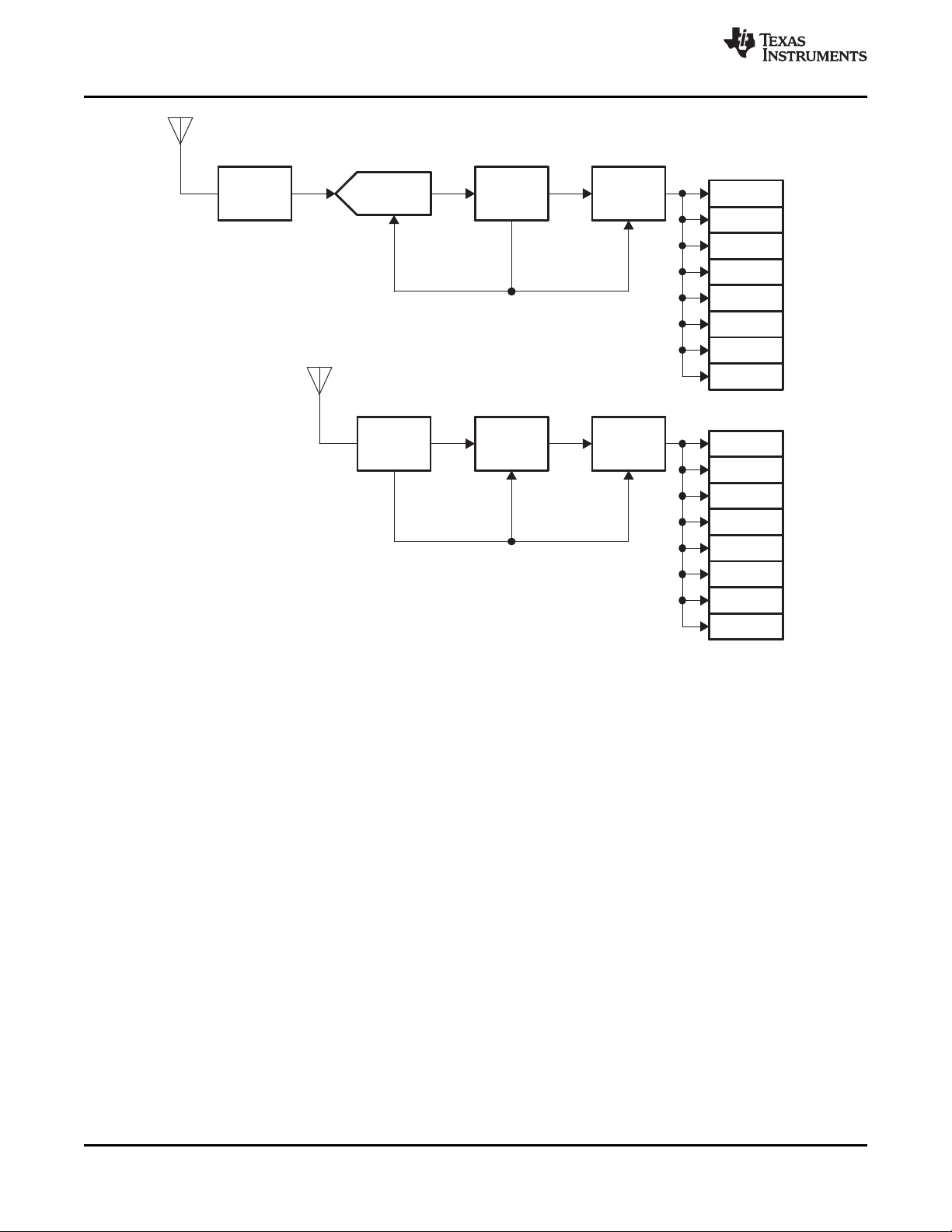
Analog
Receiver
ADC
PCM1802
Audio
DSP
TAS5508C TAS5111
TAS5111
TAS5111
TAS5111
TAS5111
TAS5111
TAS5111
TAS5111
AudioDSP Providesthe
MasterandBitClocks
Digital
Receiver
Audio
DSP
TAS5508C TAS5111
TAS5111
TAS5111
TAS5111
TAS5111
TAS5111
TAS5111
TAS5111
TheDigitalReceiverorthe AudioDSP
ProvidestheMasterandBitClocks
TAS5508C
SLES257–SEPTEMBER 2010
www.ti.com
Figure 2-22. Block Diagrams of Typical Systems Requiring TAS5508C Automatic AM
Interference-Avoidance Circuit
42 Description Copyright © 2010, Texas Instruments Incorporated
Submit Documentation Feedback
Product Folder Link(s): TAS5508C
Page 43

TAS5508C
www.ti.com
3 TAS5508C Controls and Status
The TAS5508C provides control and status information from both the I2C registers and device pins.
This section describes some of these controls and status functions. The I2C summary and detailed
register descriptions are contained in Section 6 and Section 7.
3.1 I2C Status Registers
The TAS5508C has two status registers that provide general device information. These are the general
status register 0 (0x01) and the error status register (0x02).
3.1.1 General Status Register (0x01)
• Device identification code
• Clip indicator – The TAS5508C has a clipping indicator. Writing to the register clears the indicator.
• Bank switching is busy.
3.1.2 Error Status Register (0x02)
• No internal errors (the valid signal is high)
• A clock error has occurred – These are sticky bits that are cleared by writing to the register.
– LRCLK error – when the number of MCLKs per LRCLK is incorrect
– SCLK error – when the number of SCLKS per LRCLK is incorrect
– Frame slip – when the number of MCLKs per LRCLK changes by more than 10 MCLK cycles
– PLL phase-lock error
• This error status register is normally used for system development only.
SLES257–SEPTEMBER 2010
3.2 TAS5508C Pin Controls
The TAS5508C provide a number of terminal controls to manage the device operation. These controls
are:
• RESET
• PDN
• BKND_ERR
• HP_SEL
• MUTE
3.2.1 Reset (RESET)
The TAS5508C is placed in the reset mode either by the power-up reset circuitry when power is applied,
or by setting the RESET terminal low.
RESET is an asynchronous control signal that restores the TAS5508C to the hard mute state (M). Master
volume is immediately set to full attenuation (there is no ramp down). Reset initiates the device reset
without an MCLK input. As long as the RESET terminal is held low, the device is in the reset state. During
reset, all I2C and serial data bus operations are ignored.
Table 3-1 shows the device output signals while RESET is active.
SIGNAL SIGNAL STATE
Valid Low
PWM P-outputs Low (M-state)
PWM M-outputs Low (M-state)
Table 3-1. Device Outputs During Reset
Copyright © 2010, Texas Instruments Incorporated TAS5508C Controls and Status 43
Submit Documentation Feedback
Product Folder Link(s): TAS5508C
Page 44

TAS5508C
SLES257–SEPTEMBER 2010
Because RESET is an asynchronous signal, clicks and pops produced during the application (the leading
edge) of RESET cannot be avoided. However, the transition from the hard mute state (M) to the
operational state is performed using a quiet start-up sequence to minimize noise. This control uses the
PWM reset and unmute sequence to shut down and start up the PWM. A detailed description of these
sequences is contained in the PWM section. If a completely quiet reset or power-down sequence is
desired, MUTE should be applied before applying RESET.
The rising edge of the reset pulse begins device initialization before the transition to the operational mode.
During device initialization, all controls are reset to their initial states. Table 3-2 shows the default control
settings following a reset.
Clock register Not valid
High pass Disabled
Unmute from clock error Hard unmute
PSVC Hi-Z Disabled
Post DAP detection automute Enabled
Eight Ch PreDAP detection automute Enabled
De-emphasis De-emphasis disabled
Channel configuration control Configured for the default setting
Headphone configuration control Configured for the default setting
Serial data interface format I2S 24 bit
Individual channel mute No channels are muted
Automute delay 5 ms
Automute threshold 1 < 8 bits
Automute threshold 2 Same as automute threshold 1
Modulation limit Maximum modulation limit of 97.7%
Six- (or eight – low) channel configuration Eight channels
Slew rate limit Disengaged for all channels
Interchannel delay –32, 0, –16, 16, –24, 8, –8, –24
Shutdown PWM on error Enabled
Volume and mute update rate Volume ramp 85 ms
Treble and bass slew rate Update every 1.31 ms
Bank switching Manual bank selection is enabled
Auto bank switching map All channels use bank 1
Biquad coefficients (5508) Set to all pass
Input mixer coefficients Input N -> Channel N, no attenuation
Output mixer coefficients Channel N -> Output N, no attenuation
Subwoofer sum into Ch1 and Ch2 (5508) Gain of 0
Ch1 and Ch2 sum in subwoofer (5508) Gain of 0
Bass and treble bypass Gain of 1
Bass and treble inline Gain of 0
DRC bypass (5508) Gain of 1
DRC inline (5508) Gain of 0
DRC (5508) DRC disabled, default values
www.ti.com
Table 3-1. Device Outputs During Reset (continued)
SIGNAL SIGNAL STATE
SDA Signal input (not driven)
Table 3-2. Values Set During Reset
CONTROL SETTING
44 TAS5508C Controls and Status Copyright © 2010, Texas Instruments Incorporated
Submit Documentation Feedback
Product Folder Link(s): TAS5508C
Page 45

TAS5508C
www.ti.com
After the initialization time, the TAS5508C starts the transition to the operational state with the master
volume set at mute.
Because the TAS5508C has an external crystal time base, following the release of RESET, the
TAS5508C sets the MCLK and data rates and performs the initialization sequences. The PWM outputs
are held at a mute state until the master volume is set to a value other than mute via I2C.
SLES257–SEPTEMBER 2010
Table 3-2. Values Set During Reset (continued)
CONTROL SETTING
Master volume Mute
Individual channel volumes 0 dB
All bass and treble Indexes 0x12 neutral
Treble filter sets Filter set 3
Bass filter sets Filter set 3
Loudness (5508) Loudness disabled, default values
AM interference enable Disabled
AM interference IF 455
AM interference select sequence 1
Tuned frequency and mode 0000, BCD
Subwoofer PSVC control Enabled
PSVC and PSVC range Disabled/0 dB
3.2.2 Power Down (PDN)
The TAS5508C can be placed into the power-down mode by holding the PDN terminal low. When the
power-down mode is entered, both the PLL and the oscillator are shut down. Volume is immediately set to
full attenuation (there is no ramp down). This control uses the PWM mute sequence that provides a low
click and pop transition to the hard mute state (M). A detailed description of the PWM mute sequence is
contained in the PWM section.
Power down is an asynchronous operation that does not require MCLK to go into the power-down state.
To initiate the power-up sequence requires MCLK to be operational and the TAS5508C to receive 5
MCLKs prior to the release of PDN.
As long as the PDN terminal is held low, the device is in the power-down state with the PWM outputs in a
hard mute (M) state. During power down, all I2C and serial data bus operations are ignored. Table 3-3
shows the device output signals while PDN is active.
Table 3-3. Device Outputs During Power Down
SIGNAL SIGNAL STATE
Valid Low
PWM P-outputs M-state = low
PWM M-outputs M-state = low
SDA Signal input
PSVC M-state = low
Following the application of PDN, the TAS5508C does not perform a quiet shutdown to prevent clicks and
pops produced during the application (the leading edge) of this command. The application of PDN
immediately performs a PWM stop. A quiet stop sequence can be performed by first applying MUTE
before PDN.
When PDN is released, the system goes to the end state specified by MUTE and BKND_ERR pins and
the I2C register settings.
Copyright © 2010, Texas Instruments Incorporated TAS5508C Controls and Status 45
Submit Documentation Feedback
Product Folder Link(s): TAS5508C
Page 46
TAS5508C
SLES257–SEPTEMBER 2010
The crystal time base allows the TAS5508C to determine the CLK rates. Once these rates are
determined, the TAS5508C unmutes the audio.
3.2.3 Back-End Error (BKND_ERR)
Back-end error is used to provide error management for back-end error conditions. Back-end error is a
level-sensitive signal. Back-end error can be initiated by bringing the BKND_ERR terminal low for a
minimum 5 MCLK cycles. When BKND_ERR is brought low, the PWM sets either six or eight channels
into the PWM back-end error state. This state is described in Section 2.12. Once the back-end error
sequence is initiated, a delay of 5 ms is performed before the system starts the output re-initialization
sequence. After the initialization time, the TAS5508C begins normal operation. Back-end error does not
affect other PWM modulator operations.
The number of channels that are affected by the BKND_ERR signal depends on the 6-channel
configuration signal. If the I2C setting 6-channel configuration is false, the TAS5508C places all eight
PWM outputs in the PWM back-end error state, while not affecting any other internal settings or
operations. If the I2Csetting six configuration is true, the TAS5508C brings the PWM outputs 1–6 to a
back-end error state, while not affecting any other internal settings or operations. Table 3-4 shows the
device output signal states during back-end error.
Table 3-4. Device Outputs During Back-End Error
SIGNAL SIGNAL STATE
Valid Low
PWM P-outputs M-state – low
PWM M-outputs M-state – low
HPPWM P-outputs M-state – low
HPPWM M-outputs M-state – low
SDA Signal input (not driven)
www.ti.com
3.2.4 Speaker/Headphone Selector (HP_SEL)
The HP_SEL terminal enables the headphone output or the speaker outputs. The headphone output
receives the processed data output from DAP and PWM channels 1 and 2.
In 6-channel configuration, this feature does not affect the two lineout channels.
When low, the headphone output is enabled. In this mode, the speaker outputs are disabled. When high,
the speaker outputs are enabled and the headphone is disabled.
Changes in the pin logic level result in a state change sequence using soft mute to the hard mute (M)
state for both speaker and headphone followed by a soft unmute.
When HP_SEL is low, the configuration of channels 1 and 2 is defined by the headphone configuration
register. When HP_SEL is high, the channel-1 and -2 configuration registers define the configuration of
channels 1 and 2.
3.2.5 Mute (MUTE)
The mute control provides a noiseless volume ramp to silence. Releasing mute provides a noiseless ramp
to previous volume. The TAS5508C has both master and individual channel mute commands. A terminal
is also provided for the master mute. The active-low master mute I2C register and the MUTE terminal are
logically ORed together. If either is set to low, a mute on all channels is performed. The master mute
command operates on all channels regardless of whether the system is in the 6- or 8-channel
configuration.
When MUTE is invoked, the PWM output stops switching and then goes to an idle state.
46 TAS5508C Controls and Status Copyright © 2010, Texas Instruments Incorporated
Submit Documentation Feedback
Product Folder Link(s): TAS5508C
Page 47
TAS5508C
www.ti.com
The master mute terminal is used to support a variety of other operations in the TAS5508C, such as
setting the interchannel delay, the biquad coefficients, the serial interface format, and the clock rates. A
mute command by the master mute terminal, individual I2C mute, the AM interference mute sequence, the
bank switch mute sequence, or automute overrides an unmute command or a volume command. While a
mute is active, the commanded channels are placed in a mute state. When a channel is unmuted, it goes
to the last commanded volume setting that has been received for that channel.
3.3 Device Configuration Controls
The TAS5508C provides a number of system configuration controls that are set at initialization and
following a reset.
• Channel configuration
• Headphone configuration
• Audio system configurations
• Recovery from clock error
• Power-supply volume-control enable
• Volume and mute update rate
• Modulation index limit
• Interchannel delay
• Master clock and data rate controls
• Bank controls
SLES257–SEPTEMBER 2010
3.3.1 Channel Configuration Registers
For the TAS5508C to have full control of the power stages, registers 0x05 to 0x0C must be programmed
to reflect the proper power stage and how each one should be controlled. There are eight channel
configuration registers, one for each channel.
The primary reason for using these registers is that different power stages require different handling
during start-up, mute/unmute, shutdown, and error recovery. The TAS5508C must select the sequence
that gives the best click and pop performance and ensures that the bootstrap capacitor is charged
correctly during start-up. This sequence depends on which power stage is present at the TAS5508C
output.
Table 3-5. Description of the Channel Configuration Registers (0x05 to 0x0C)
BIT DESCRIPTION
D7 Enable/disable error recovery sequence. In case the BKND_RECOVERY pin is pulled low, this register determines if this
channel is to follow the error recovery sequence or to continue with no interruption.
D6 Determines if the power stage needs the TAS5508C VALID pin to go low to reset the power stage. Some power stages can be
reset by a combination of PWM signals. For these devices, it is recommended to set this bit low, because the VALID pin is
shared for power stages. This provides better control of each power stage.
D5 Determines if the power stage needs the TAS5508C VALID pin to go low to mute the power stage. Some power stages can be
muted by a combination of PWM signals. For these devices, it is recommended to set this bit low, because the VALID pin is
shared for power stages. This provides better control of each power stage.
D4 Inverts the PWM output. Inverting the PWM output can be an advantage if the power stage input pin is opposite the TAS5508C
PWM pinout. This makes routing on the PCB easier. To keep the phase of the output, the speaker terminals must also be
inverted.
D3 The power stage TAS5182 has a special PWM input. To ensure that the TAS5508C has full control in all occasions, the PWM
output must be remapped.
D2 Can be used to handle click and pop for some applications.
D1 This bit is normally used together with D2. For some power stages, both PWM signals must be high to get the desired operation
of both speaker outputs to be low. This bit sets the PWM outputs high-high during mute.
D0 Not used
Copyright © 2010, Texas Instruments Incorporated TAS5508C Controls and Status 47
Submit Documentation Feedback
Product Folder Link(s): TAS5508C
Page 48

TAS5508C
SLES257–SEPTEMBER 2010
Table 3-6 lists the optimal setting for each output-stage configuration. Note that the default value is
applicable in all configurations except the TAS5182 SE/BTL configuration.
Table 3-6. Recommended TAS5508C Configurations for Texas Instruments Power Stages
DEVICE ERROR RECOVERY CONFIGURATION D7 D6 D5 D4 D3 D2 D1 D0
TAS5111
RES
(default)
AUT
RES
TAS5112
AUT
TAS5182 RES
BTL 1 1 1 0 0 0 0 0
SE 1 1 1 0 0 0 0 0
BTL 0 1 1 0 0 0 0 0
SE 0 1 1 0 0 0 0 0
BTL 1 1 0 0 0 0 0 0
SE 1 1 0 0 0 0 0 0
BTL 0 1 0 0 0 0 0 0
SE 0 1 0 0 0 0 0 0
BTL 1 1 1 0 1 0 0 0
SE 1 1 1 0 1 0 0 0
RES: To recover from a shutdown, the output stage requires VALID to go low.
AUT: The power stage can auto-recover from a shutdown.
BTL: Bridge-tied load configuration
SE: Single-ended configuration
www.ti.com
3.3.2 Headphone Configuration Registers
The headphone configuration controls are identical to the speaker configuration controls. The headphone
configuration control settings are used in place of the speaker configuration control settings for channels 1
and 2 when the headphones are selected. However, only one configuration setting for headphones is
used, and that is the default setting.
3.3.3 Audio System Configurations
The TAS5508C can be configured to comply with various audio systems: 5.1-channel system, 6-channel
system, 7.1-channel system, and 8-channel system.
The audio system configuration is set in the general control register (0xE0). Bits D31–D4 must be zero
and D0 is don't care.
D3 Determines if SUB is to be controlled by PSVC
D2 Enables/disables power-supply volume control
D1 Sets number of speakers in the system, including possible line outputs
D3–D1 must be configured for the audio system in the application, as shown in Table 3-7.
48 TAS5508C Controls and Status Copyright © 2010, Texas Instruments Incorporated
Submit Documentation Feedback
Product Folder Link(s): TAS5508C
Page 49

TAS5508C
www.ti.com
Table 3-7. Audio System Configuration (General Control Register 0xE0)
Audio System D31–D4 D3 D2 D1 D0
6 channels or 5.1 not using PSVC 0 0 0 1 X
6 channels using PSVC 0 0 1 1 X
5.1 system using PSVC 0 1 1 1 X
8 channels or 7.1 not using PSVC (default) 0 0 0 0 X
8 channels using PSVC 0 0 1 0 X
7.1 system using PSVC 0 1 1 0 X
3.3.3.1 Using Line Outputs in 6-Channel Configurations
The audio system can be configured for a 6-channel configuration (with 2 lineouts) by writing a 1 to bit D1
of register 0xE0 (general control register). In this configuration, channel-5 and -6 processing are exactly
the same as the other channels, except that the master volume has no effect.
Note that in 6-channel configuration, channels 5 and 6 are unaffected by back-end error (BKND_ERR
goes low).
To use channels 5 and 6 as unprocessed lineouts, the following setup should be done:
• Channel-5 volume and channel-6 volume should be set for a constant output such as 0 dB.
• Bass and treble for channels 5 and 6 can be used if desired.
• DRC1 should be bypassed for channels 5 and 6.
• If enabled, the loudness function shapes the response of channels 5 and 6. However, the amplitude of
5 and 6 is not used in determining the loudness response.
• If a down mix is desired on channels 5 and 6 as lineout, the down mixing can be performed using the
channel-5 and channel-6 input mixers.
• The operation of the channel-5 and -6 biquads is unaffected by the 6-/8-channel configuration setting.
SLES257–SEPTEMBER 2010
3.3.4 Recovery from Clock Error
The TAS5508C can be set either to perform a volume ramp up during the recovery sequence of a clock
error or simply to come up in the last state (or desired state if a volume or tone update was in progress).
This feature is enabled via I2C system control register 0x03.
3.3.5 Power-Supply Volume-Control Enable
The power-supply volume control (PSVC) can be enabled and disabled via I2C register 0xE0. The
subwoofer PWM output can be configured to be controlled by the PSVC or digitally attenuated when
PSVC is enabled (for powered subwoofer configurations). Note that PSVC cannot be simultaneously
enabled along with unmute outputs after clock error feature.
3.3.6 Volume and Mute Update Rate
The TAS5508C has fixed soft volume and mute ramp durations. The ramps are linear. The soft volume
and mute ramp rates are adjustable by programming the I2C register 0xD0 for the appropriate number of
steps to be 512, 1024, or 2048. The update is performed at a fixed rate regardless of the sample rate.
• In normal speed, the update rate is 1 step every 4/Fs seconds.
• In double speed, the update is 1 step every 8/Fs seconds.
• In quad speed, the update is 1 step every 16/Fs seconds.
Because of processor loading, the update rate can increase for some increments by 1/Fs to 3/Fs.
However, the variance of the total time to go from 18 dB to mute is less than 25%.
Copyright © 2010, Texas Instruments Incorporated TAS5508C Controls and Status 49
Submit Documentation Feedback
Product Folder Link(s): TAS5508C
Page 50

TAS5508C
SLES257–SEPTEMBER 2010
NUMBER OF STEPS
512 46.44 ms 42.67 ms
1024 92.88 ms 85.33 ms
2048 185.76 ms 170.67 ms
3.3.7 Modulation Index Limit
PWM modulation is a linear function of the audio signal. When the audio signal is 0, the PWM modulation
is 50%. When the audio signal increases toward full scale, the PWM modulation increases toward 100%.
For negative signals, the PWM modulations fall below 50% toward 0%.
However, there is a limit to the maximum modulation possible. During the offtime period, the power stage
connected to the TAS5508C output needs to get ready for the next ontime period. The maximum possible
modulation is then set by the power stage requirements. All Texas Instruments power stages need
maximum modulation to be 97.7%. This is also the default setting of the TAS5508C. Default settings can
be changed in the modulation index register (0x16).
Note that no change should be made to this register when using Texas Instruments power stages.
3.3.8 Interchannel Delay
An 8-bit value can be programmed into each of the eight PWM interchannel delay registers to add a delay
per channel from 0 to 255 clock cycles. The delays correspond to cycles of the high-speed internal clock,
DCLK. The default values are shown in Table 3-9.
www.ti.com
Table 3-8. Volume Ramp Rates in ms
SAMPLE RATE (kHz)
44.1, 88.2, 176.4 32, 48, 96, 192
Table 3-9. Interchannel Delay Default Values
I2C SUBADDRESS CHANNEL INTERCHANNEL DELAY DEFAULT (DCLK PERIODS)
0x1B 1 –24
0x1C 2 0
0x1D 3 –16
0x1E 4 16
0x1F 5 –24
0x20 6 8
0x21 7 –8
0x22 8 24
This delay is generated in the PWM and can be changed at any time through the serial-control interface
I2C registers 0x1B–0x22. The absolute offset for channel 1 is set in I2C subaddress 0x23.
If used correctly, setting the PWM channel delay can optimize the performance of a
PurePath Digital™ amplifier system . The setting is based on both the type of back-end
power device that is used and the layout. These values are set during initialization using the
I2C serial interface. Unless otherwise noted, use the default values given in Table 3-9.
3.4 Master Clock and Serial Data Rate Controls
The TAS5508C functions only as a receiver of the MCLK (master clock), SCLK (shift clock), and LRCLK
(left/right clock) signals that control the flow of data on the four serial data interfaces. The 13.5-MHz
external crystal allows the TAS5508C to detect MCLK and the data rate automatically.
NOTE
50 TAS5508C Controls and Status Copyright © 2010, Texas Instruments Incorporated
Submit Documentation Feedback
Product Folder Link(s): TAS5508C
Page 51

TAS5508C
www.ti.com
The MCLK frequency can be 64 × Fs, 128 × Fs, 196 × Fs, 256 × Fs, 384 × Fs, 512 × Fs, or 768 × Fs.
The TAS5508C operates with the serial data interface signals LRCLK and SCLK synchronized to MCLK.
However, there is no constraint as to the phase relationship of these signals. The TAS5508C accepts a
64 × Fs SCLK rate and a 1 × Fs LRCLK.
If the phase of SCLK or LRCLK drifts more than ±10 MCLK cycles since the last reset, the TAS5508C
senses a clock error and resynchronizes the clock timing.
The clock and serial data interface have several control parameters:
• MCLK ratio (64 Fs, 128 Fs, 196 Fs, 256 Fs, 384 Fs, 512 Fs, or 768 Fs) – I2C parameter
• Data rate (32, 38, 44.1,48, 88.2, 96, 176.4, 192 kHz) – I2C parameter
• AM mode enable/disable – I2C parameter
During AM interference avoidance, the clock control circuitry uses three other configuration inputs:
• Tuned AM frequency (for AM interference avoidance) (550 - 1750 kHz) – I2C parameter
• Frequency set select (1–4) – I2C parameter
• Sample rate – I2C parameter or auto-detected
3.4.1 PLL Operation
The TAS5508C uses two internal clocks generated by two internal phase-locked loops (PLLs), the digital
PLL (DPLL) and the analog PLL (APLL). The APLL provides the reference clock for the PWM. The DPLL
provides the reference clock for the digital audio processor and the control logic.
SLES257–SEPTEMBER 2010
The master clock MCLK input provides the input reference clock for the APLL. The external 13.5-MHz
crystal provides the input reference clock for the DPLL. The crystal provides a time base to support a
number of operations, including the detection of the MCLK ratio, the data rate, and clock error conditions.
The crystal time base provides a constant rate for all controls and signal timing.
Even if MCLK is not present, the TAS5508C can receive and store I2C commands and provide status.
3.5 Bank Controls
The TAS5508C permits the user to specify and assign sample-rate-dependent parameters for biquad,
loudness, DRC, and tone in one of three banks that can be manually selected or selected automatically
based on the data sampling rate. Each bank can be enabled for one or more specific sample rates via I2C
bank control register 0x40. Each bank set holds the following values:
• Coefficients for seven biquads (7 × 5 = 35 coefficients) for each of the eight channels (registers
0x51–0x88)
• Coefficients for one loudness biquad (register 0x95)
• DRC1 energy and (1 – energy) values (register 0x98)
• DRC1 attack, (1 – attack), decay, (1 – decay) values (register 0x9C)
• DRC2 energy and (1 – energy) values (register 0x9D)
• DRC2 attack, (1 – attack), decay, (1 – decay) values (register 0xA1)
• Five bass filter-set selections (register 0xDA)
• Five treble filter-set selections (register 0xDC)
The default selection for bank control is manual bank with bank 1 selected. Note that if bank switching is
used, bank 2 and bank 3 must be programmed on power up, because the default values are all zeroes. If
bank switching is used and bank 2 and bank 3 are not programmed correctly, then the output of the
TAS5508C could be muted when switching to those banks.
Copyright © 2010, Texas Instruments Incorporated TAS5508C Controls and Status 51
Submit Documentation Feedback
Product Folder Link(s): TAS5508C
Page 52

TAS5508C
SLES257–SEPTEMBER 2010
3.5.1 Manual Bank Selection
The three bank selection bits of the bank control register allow the appropriate bank to be manually
selected (000 = bank 1, 001 = bank 2, 010 = bank 3). In the manual mode, when a write occurs to the
biquad, DRC, or loudness coefficients, the currently selected bank is updated. If audio data is streaming to
the TAS5508C during a manual bank selection, the TAS5508C first performs a mute sequence, then
performs the bank switch, and finally restores the volume using an unmute sequence.
A mute command initiated by the bank-switch mute sequence overrides an unmute command or a volume
command. While a mute is active, the commanded channels are muted. When a channel is unmuted, the
volume level goes to the last commanded volume setting that has been received for that channel.
If MCLK or SCLK is stopped, the TAS5508C performs a bank-switch operation. If the clocks start up once
the manual bank-switch command has been received, the bank-switch operation is performed during the
5-ms, silent-start sequence.
3.5.2 Automatic Bank Selection
To enable automatic bank selection, a value of 3 is written into the bank selection bits of the bank control
register. Banks are associated with one or more sample rates by writing values into the bank 1 or bank 2
data-rate selection registers. The automatic bank selection is performed when a frequency change is
detected according to the following scheme:
1. The system scans bank-1 data-rate associations to see if bank 1 is assigned for that data rate.
2. If bank 1 is assigned, then the bank-1 coefficients are loaded.
3. If bank 1 is not assigned, the system scans bank 2 to see if bank 2 is assigned for that data rate.
4. If bank 2 is assigned, the bank 2 coefficients are loaded.
5. If bank 2 is not assigned, the system loads the bank 3 coefficients.
www.ti.com
The default is that all frequencies are enabled for bank 1. This default is expressed as a value of all 1s in
the bank-1 auto-selection byte and all 0s in the bank-2 auto-selection byte.
3.5.2.1 Coefficient Write Operations While Automatic Bank Switch Is Enabled
In automatic mode, if a write occurs to the tone, EQ, DRC, or loudness coefficients, the bank that is
written to is the current bank.
3.5.3 Bank Set
Bank set is used to provide a secure way to update the bank coefficients in both the manual and
automatic switching modes without causing a bank switch to occur. Bank-set mode does not alter the
current bank register mapping. It simply enables any bank coefficients to be updated while inhibiting any
bank switches from taking place. In manual mode, this enables the coefficients to be set without switching
banks. In automatic mode, this prevents a clock error or data rate change from corrupting a bank
coefficient write.
To update the coefficients of a bank, a value of 4, 5, or 6 is written into in the bank selection-bits of the
bank control register. This enables the tone, EQ, DRC, and loudness coefficient values of bank 1, 2, or 3,
respectively, to be updated.
Once the coefficients of the bank have been updated, the bank-selection bits are then returned to the
desired manual or automatic bank-selection mode.
3.5.4 Bank-Switch Timeline
After a bank switch is initiated (manual or automatic), no I2C writes to the TAS5508C should occur before
a minimum of 186 ms. This value is determined by the volume ramp rates for a particular sample rate.
52 TAS5508C Controls and Status Copyright © 2010, Texas Instruments Incorporated
Submit Documentation Feedback
Product Folder Link(s): TAS5508C
Page 53

TAS5508C
www.ti.com
3.5.5 Bank-Switching Example 1
Problem: The audio unit containing a TAS5508C needs to handle different audio formats with different
sample rates. Format #1 requires Fs = 32 kHz, format #2 requires Fs = 44.1 kHz, and format #3 requires
Fs = 48 kHz. The sample-rate-dependent parameters in the TAS5508C require different coefficients and
data depending on the sample rate.
Strategy: Use the TAS5508C bank-switching feature to allow for managing and switching three banks
associated with the three sample rates, 32 kHz (bank 1), 44.1 kHz (bank 2), and 48 kHz (bank 3).
One possible algorithm is to generate, load, and automatically manage bank switching for this problem:
1. Generate bank-related coefficients for sample rates of 32 kHz, 44.1 kHz, and 48 kHz, and include the
same in the microprocessor-based TAS5508C I2C firmware.
2. On TAS5508C power up or reset, the microprocessor runs the following TAS5508C initialization code:
(a) Update bank 1 (write 0x00048040 to register 0x40).
(b) Write bank-related I2C registers with appropriate values for bank 1.
(c) Write bank 2 (write 0x0005 8040 to register 0x40).
(d) Load bank-related I2C registers with appropriate values for bank 2.
(e) Write bank 3 (write 0x00068040 to register 0x40).
(f) Load bank-related I2C registers with appropriate values for bank 3.
(g) Select automatic bank switching (write 0x0003 8040 to register 0x40).
3. When the audio media changes, the TAS5508C automatically detects the incoming sample rate and
automatically switches to the appropriate bank.
SLES257–SEPTEMBER 2010
In this example, any sample rates other than 32 kHz and 44.1 kHz use bank 3. If other sample rates are
used, then the banks must be set up differently.
3.5.6 Bank-Switching Example 2
Problem: The audio system uses all of the sample rates supported by the TAS5508C. How can the
automatic bank switching be set up to handle this situation?
Strategy: Use the TAS5508C bank-switching feature to allow for managing and switching three banks
associated with sample rates as follows:
• Bank 1: Coefficients for 32 kHz, 38 kHz, 44.1 kHz, and 48 kHz
• Bank 2: Coefficients for 88.2kHz and 96 kHz
• Bank 3: Coefficients for 176.4 kHz and 192 kHz
One possible algorithm is to generate, load, and automatically manage bank switching for this problem:
1. Generate bank-related coefficients for sample rates 48 kHz (bank 1), 96 kHz (bank 2), and 192 kHz
(bank 3) and include the same in the microprocessor-based TAS5508C I2C firmware.
2. On TAS5508C power up or reset, the microprocessor runs the following TAS5508C initialization code:
(a) Update bank 1 (write 0x0004F00C to register 0x40).
(b) Write bank-related I2C registers with appropriate values for bank 1.
(c) Write bank 2 (write 0x0005 F00C to register 0x40).
(d) Load bank-related I2C registers with appropriate values for bank 2.
(e) Write bank 3 (write 0x0006F00C to register 0x40).
(f) Load bank-related I2C registers with appropriate values for bank 3.
(g) Select automatic bank switching (write 0x0003 F00C to register 0x40).
3. When the audio media changes, the TAS5508C automatically detects the incoming sample rate and
automatically switches to the appropriate bank.
Copyright © 2010, Texas Instruments Incorporated TAS5508C Controls and Status 53
Submit Documentation Feedback
Product Folder Link(s): TAS5508C
Page 54

TAS5508C
SLES257–SEPTEMBER 2010
www.ti.com
54 TAS5508C Controls and Status Copyright © 2010, Texas Instruments Incorporated
Submit Documentation Feedback
Product Folder Link(s): TAS5508C
Page 55

TAS5508C
www.ti.com
SLES257–SEPTEMBER 2010
4 Electrical Specifications
4.1 Absolute Maximum Ratings
Supply voltage, DVDD and DVD_PWM –0.3 V to 3.6 V
Supply voltage, AVDD_PLL –0.3 V to 3.6 V
3.3-V digital input –0.5 V to DVDD + 0.5 V
Input voltage 5 V tolerant
1.8 V LVCMOS
I
IK
I
OK
T
A
T
stg
(1) Stresses beyond those listed under Absolute Maximum Ratings may cause permanent damage to the device. These are stress ratings
(2) 5-V tolerant inputs are RESET, PDN, MUTE, HP_SEL, SCLK, LRCLK, MCLK, SDIN1, SDIN2, SDIN3, SDIN4, SDA, and SCL.
(3) VRA_PLL, VRD_PLL, VR_DPLL, VR_DIG, VR_PWM
(4) VREF is a 1.8-V supply derived from regulators internal to the TAS5508C chip. VREF is on terminals VRA_PLL, VRD_PLL, VR_DPLL,
Input clamp current (VI< 0 or VI> 1.8 V ±20 mA
Output clamp current (VO< 0 or VO> 1.8 V) ±20 mA
Operating free-air temperature 0°C to 70°C
Storage temperature range –65°C to 150°C
only, and functional operation of the device at these or any other conditions beyond those indicated under Recommended Operating
Conditions is not implied. Exposure to absolute-maximum-rated conditions for extended periods may affect device reliability.
VR_DIG, and VR_PWM. These terminals are provided to permit use of external filter capacitors, but should not be used to source power
to external devices.
4.2 Dissipation Rating Table (High-k Board, 105°C Junction)
PACKAGE
PAG 1869 mW 23.36 mW/°C 818 mW
TA≤ 25°C DERATING FACTOR TA= 70°C
POWER RATING ABOVE TA= 25°C POWER RATING
(1)
(2)
digital input –0.5 V to 6 V
(3)
–0.5 V to VREF
(4)
+ 0.5 V
4.3 Dynamic Performance At Recommended Operating Conditions at 25°C
PARAMETER TEST CONDITIONS MIN NOM MAX UNIT
Dynamic range 32 kHz to 192 kHz TAS5508C + TAS5111 A-weighted 102 dB
Total harmonic distortion
Frequency response dB
TAS5111 at 1 W 0.1%
TAS5508C ouput 0.01%
32-kHz to 96-kHz sample rates ±0.1
176.4, 192-kHz sample rates ±0.2
4.4 Recommended Operating Conditions
MIN NOM MAX UNIT
Digital supply voltage, DVDD and DVDD_PWM 3 3.3 3.6 V
Analog supply voltage, AVDD_PLL 3 3.3 3.6 V
3.3 V 2
VIHHigh-level input voltage 5-V tolerant
1.8-V LVCMOS (XTL_IN) 1.26
3.3 V 0.8
VILLow-level input voltage 5-V tolerant
1.8-V (XTL_IN) 0.54
TAOperating ambient-air temperature range 0 25 70 °C
TJOperating junction temperature range –20 105 °C
(1) 5-V tolerant inputs are RESET, PDN, MUTE, HP_SEL, SCLK, LRCLK, MCLK, SDIN1, SDIN2, SDIN3, SDIN4, SDA, and SCL.
(1)
(1)
2 V
0.8 V
Copyright © 2010, Texas Instruments Incorporated Electrical Specifications 55
Submit Documentation Feedback
Product Folder Link(s): TAS5508C
Page 56

TAS5508C
SLES257–SEPTEMBER 2010
www.ti.com
4.5 Electrical Characteristics
Over recommended operating conditions (unless otherwise noted)
PARAMETER TEST CONDITIONS MIN TYP MAX UNIT
VOHHigh-level output voltage V
VOLLow-level output voltage V
I
High-impedance output current 3.3-V TTL ±20 mA
OZ
3.3-V TTL and 5 V
1.8-V LVCMOS (XTL_OUT) IOH= –0.55 mA 1.44
3.3-V TTL and 5 V
1.8-V LVCMOS (XTL_OUT) IOL= 0.75 mA 0.5
3.3-V TTL VI= V
I
Low-level input current 1.8-V LVCMOS (XTL_IN) VI= V
IL
5 V tolerant
3.3-V TTL VI= V
I
High-level input current 1.8-V LVCMOS (XTL_IN) VI= V
IH
5 V tolerant
Digital supply voltage, DVDD mA
I
Input supply current
DD
Analog supply voltage, AVDD mA
(1) 5-V tolerant outputs are SCL and SDA.
(2) 5-V tolerant inputs are RESET, PDN, MUTE, HP_SEL, SCLK, LRCLK, MCLK, SDIN1, SDIN2, SDIN3, SDIN4, SDA, and SCL.
(1)
tolerant IOH= –4 mA 2.4
(1)
tolerant IOL= 4 mA 0.5
IL
(2)
(2)
IL
VI= 0 V, DVDD = 3 V ±1
IH
IH
VI= 5.5 V, DVDD = 3 V ±20
±1
±1 mA
±1
±1 mA
Fs = 48 kHz 140
Fs = 96 kHz 150
Fs = 192 kHz 155
Power down 8
Normal 20
Power down 2
4.6 PWM Operation
Over recommended operating conditions
PARAMETER TEST CONDITIONS MODE VALUE UNIT
32-kHz data rate ±4% 12× sample rate 384 kHz
Output sample rate 1×–8× oversampled 44.1-, 88.2-, 176.4-kHz data rate ±4% 8×, 4×, or 2× sample rate 352.8 kHz
48-, 96-, 192-kHz data rate ±4% 8×, 4×, or 2× sample rate 384 kHz
4.7 Switching Characteristics
4.7.1 Clock Signals
PLL input parameters and external filter components over recommended operating conditions (unless otherwise noted)
PARAMETER TEST CONDITIONS MIN TYP MAX UNIT
f
XTALI
f
MCLKI
(1) See the TAS5508C Example Application Schematic, Section 8.
Frequency, XTAL IN Only use 13.5-MHz crystal ≤1000 ppm 13.5 MHz
Frequency, MCLK (1/t
) 2 50 MHz
cyc2
MCLK duty cycle 40% 50% 60%
MCLK minimum high time 5 ns
MCLK minimum low time 5 ns
≥2-V MCLK = 49.152 MHz, within the min
and max duty cycle constraints
≤0.8-V MCLK = 49.152 MHz, within the min
and max duty cycle constraints
LRCLK allowable drift before LRCLK reset 10 MCLKs
External PLL filter capacitor C1 SMD 0603 Y5V 100 nF
External PLL filter capacitor C2 SMD 0603 Y5V 10 nF
External PLL filter resistor R SMD 0603, metal film 200 Ω
External VRA_PLL decoupling SMD, Y5V 100 nF
(1)
56 Electrical Specifications Copyright © 2010, Texas Instruments Incorporated
Submit Documentation Feedback
Product Folder Link(s): TAS5508C
Page 57

t
h1
t
su1
t
su2
t
h2
SCLK
(Input)
LRCLK
(Input)
SDIN1
SDIN2
SDIN3
T0026-01
TAS5508C
www.ti.com
4.7.2 Serial Audio Port
Serial audio port slave mode over recommended operating conditions (unless otherwise noted)
PARAMETER TEST CONDITIONS MIN TYP MAX UNIT
f
SCLK input frequency CL= 30 pF,SCLK = 64 × Fs 2.048 12.288 MHz
SCLKIN
t
Setup time, LRCLK to SCLK rising edge 10 ns
su1
t
Hold time, LRCLK from SCLK rising edge 10 ns
h1
t
Setup time, SDIN to SCLK rising edge 10 ns
su2
t
Hold time, SDIN from SCLK rising edge 10 ns
h2
LRCLK frequency 32 48 192 kHz
SCLK duty cycle 40% 50% 60%
LRCLK duty cycle 40% 50% 60%
SCLK rising edges between LRCLK rising edges 64 64
LRCLK clock edge with respect to the falling edge of SCLK
SCLK period
SLES257–SEPTEMBER 2010
SCLK
edges
–1/4 1/4
Figure 4-1. Slave Mode Serial Data Interface Timing
Copyright © 2010, Texas Instruments Incorporated Electrical Specifications 57
Submit Documentation Feedback
Product Folder Link(s): TAS5508C
Page 58
SCL
SDA
t
w(H)
t
w(L)
t
r
t
f
t
su1
t
h1
T0027-01
SCL
SDA
t
h2
t
(buf)
t
su2
t
su3
Start
Condition
Stop
Condition
T0028-01
TAS5508C
SLES257–SEPTEMBER 2010
4.7.3 I2C Serial Control Port Operation
Timing characteristics for I2C interface signals over recommended operating conditions
PARAMETER TEST CONDITIONS MIN MAX UNIT
f
t
t
t
t
t
t
t
t
t
t
C
SCL
w(H)
w(L)
r
f
su1
h1
(buf)
su2
h2
su3
L
Frequency, SCL No wait states 400 kHz
Pulse duration, SCL high 0.6 ms
Pulse duration, SCL low 1.3 ms
Rise time, SCL and SDA 300 ns
Fall time, SCL and SDA 300 ns
Setup time, SDA to SCL 100 ns
Hold time, SCL to SDA 0 ns
Bus free time between stop and start condition 1.3 ms
Setup time, SCL to start condition 0.6 ms
Hold time, start condition to SCL 0.6 ms
Setup time, SCL to stop condition 0.6 ms
Load capacitance for each bus line 400 pF
www.ti.com
Figure 4-2. SCL and SDA Timing
Figure 4-3. Start and Stop Conditions Timing
58 Electrical Specifications Copyright © 2010, Texas Instruments Incorporated
Submit Documentation Feedback
Product Folder Link(s): TAS5508C
Page 59

PDN
M-State
t
su
t <300 s
p(DMSTATE)
m
T0030-01
TAS5508C
www.ti.com
SLES257–SEPTEMBER 2010
4.7.4 Reset Timing (RESET)
Control signal parameters over recommended operating conditions (unless otherwise noted)
PARAMETER MIN TYP MAX UNIT
t
r(DMSTATE)
t
w(RESET)
t
r(I2C_ready)
t
r(run)
NOTE: Because a crystal time base is used, the system determines the CLK rates. Once the data rate and master clock ratio
Time to M-STATE low 370 ns
Pulse duration, RESET active 400 None ns
Time to enable I2C 3 ms
Device start-up time 10 ms
is determined, the system outputs audio if a master volume command is issued.
Figure 4-4. Reset Timing
4.7.5 Power-Down (PDN) Timing
Control signal parameters over recommended operating conditions (unless otherwise noted)
PARAMETER MIN TYP MAX UNIT
t
p(DMSTATE)
t
su
Time to M-STATE low 300 ms
Number of MCLKs preceding the release of PDN 5
Device start-up time 120 ms
Figure 4-5. Power-Down Timing
Copyright © 2010, Texas Instruments Incorporated Electrical Specifications 59
Submit Documentation Feedback
Product Folder Link(s): TAS5508C
Page 60
ERR_RCVRY
t
p(valid_low)
M-State
t
w(ER)
t
p(valid_high)
Normal
Operation
Normal
Operation
T0031-01
t
d(VOL)
VOLUME
MUTE
Normal
Operation
M-State
Normal
Operation
t
d(VOL)
T0032-01
TAS5508C
SLES257–SEPTEMBER 2010
4.7.6 Back-End Error (BKND_ERR)
Control signal parameters over recommended operating conditions (unless otherwise noted)
PARAMETER MIN TYP MAX UNIT
t
w(ER)
t
p(valid_low)
t
p(valid_high)
Pulse duration, BKND_ERR active 350 None ns
I2C programmable to be between 1 to 10 ms –25 25 % of interval
Figure 4-6. Error Recovery Timing
www.ti.com
<100 ms
4.7.7 Mute Timing (MUTE)
Control signal parameters over recommended operating conditions (unless otherwise noted)
PARAMETER MIN TYP MAX UNIT
t
Volume ramp time Defined by rate setting
d(VOL)
(1) See the Volume Treble and Base Slew Rate Register (0xD0) , Section 7.29.
Figure 4-7. Mute Timing
(1)
ms
60 Electrical Specifications Copyright © 2010, Texas Instruments Incorporated
Submit Documentation Feedback
Product Folder Link(s): TAS5508C
Page 61
t
d(VOL)
HP Volume
HP_SEL
M-State
t
d(VOL)
SpkrVolume
t
(SW)
t
d(VOL)
SpkrVolume
HP_SEL
M-State
t
d(VOL)
HP Volume
t
(SW)
(InternalDeviceState)
T0033-01
TAS5508C
www.ti.com
4.7.8 Headphone Select (HP_SEL)
Control signal parameters over recommended operating conditions (unless otherwise noted)
PARAMETER MIN MAX UNIT
t
w(MUTE)
t
d(VOL)
t
(SW)
(1) See the Volume Treble and Base Slew Rate Register (0xD0) , Section 7.29.
Pulse duration, HP_SEL active 350 None ns
Soft volume update time Defined by rate setting
Switchover time 0.2 1 ms
SLES257–SEPTEMBER 2010
(1)
ms
Copyright © 2010, Texas Instruments Incorporated Electrical Specifications 61
Figure 4-8. HP_SEL Timing
Submit Documentation Feedback
Product Folder Link(s): TAS5508C
Page 62
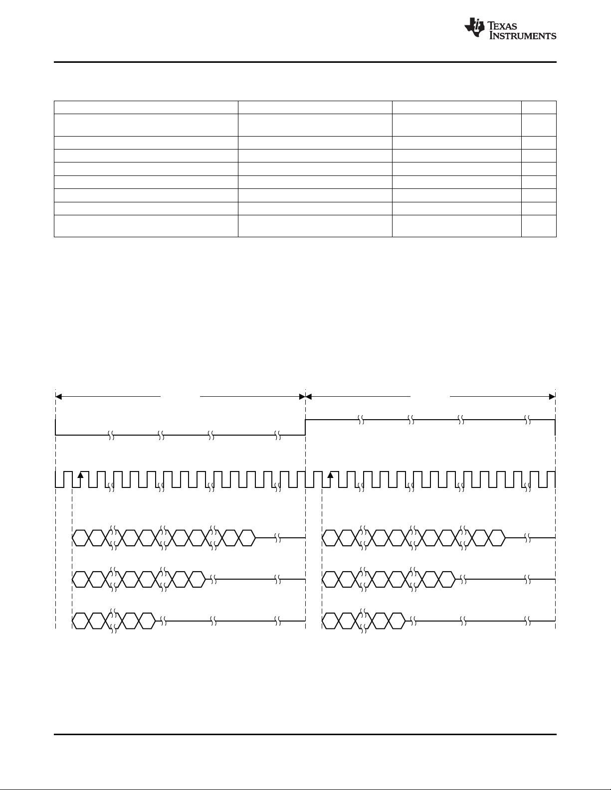
23
22
SCLK
32Clks
LRCLK(NoteReversedPhase)
LeftChannel
24-BitMode
1
19 18
20-BitMode
16-BitMode
15
14
MSB LSB
32Clks
RightChannel
2-ChannelI S(PhilipsFormat)StereoInput
2
T0034-01
5
4
9 8
1
0
0
4
5
1
0
23
22 1
19 18
15
14
MSB LSB
5
4
9 8
1
0
0
4
5
1
0
SCLK
TAS5508C
SLES257–SEPTEMBER 2010
www.ti.com
4.7.9 Volume Control
Control signal parameters over recommended operating conditions (unless otherwise noted)
PARAMETER TEST CONDITIONS MIN MAX UNIT
Maximum attenuation before mute –127 dB
Maximum gain Individual volume, master volume 18 dB
Maximum volume before the onset of clipping 0-dB input, any modulation limit 0 dB
PSVC range PSVC enabled 12, 18, or 24 dB
PSVC rate Fs
PSVC modulation Single sided
PSVC quantization 2048 Steps
PSVC PWM modulation limits PSVC range = 24 dB dB
Individual volume, master volume, or a
combination of both
6% 95%
(120 : 2048) (1944 : 2048)
4.8 Serial Audio Interface Control and Timing
4.8.1 I2S Timing
I2S timing uses LRCLK to define when the data being transmitted is for the left channel and when it is for the
right channel. LRCLK is low for the left channel and high for the right channel. A bit clock running at 64 × Fs is
used to clock in the data. There is a delay of one bit clock from the time the LRCLK signal changes state to the
first bit of data on the data lines. The data is written MSB first and is valid on the rising edge of the bit clock. The
TAS5508C masks unused trailing data bit positions.
62 Electrical Specifications Copyright © 2010, Texas Instruments Incorporated
Figure 4-9. I2S 64-Fs Format
Submit Documentation Feedback
Product Folder Link(s): TAS5508C
Page 63
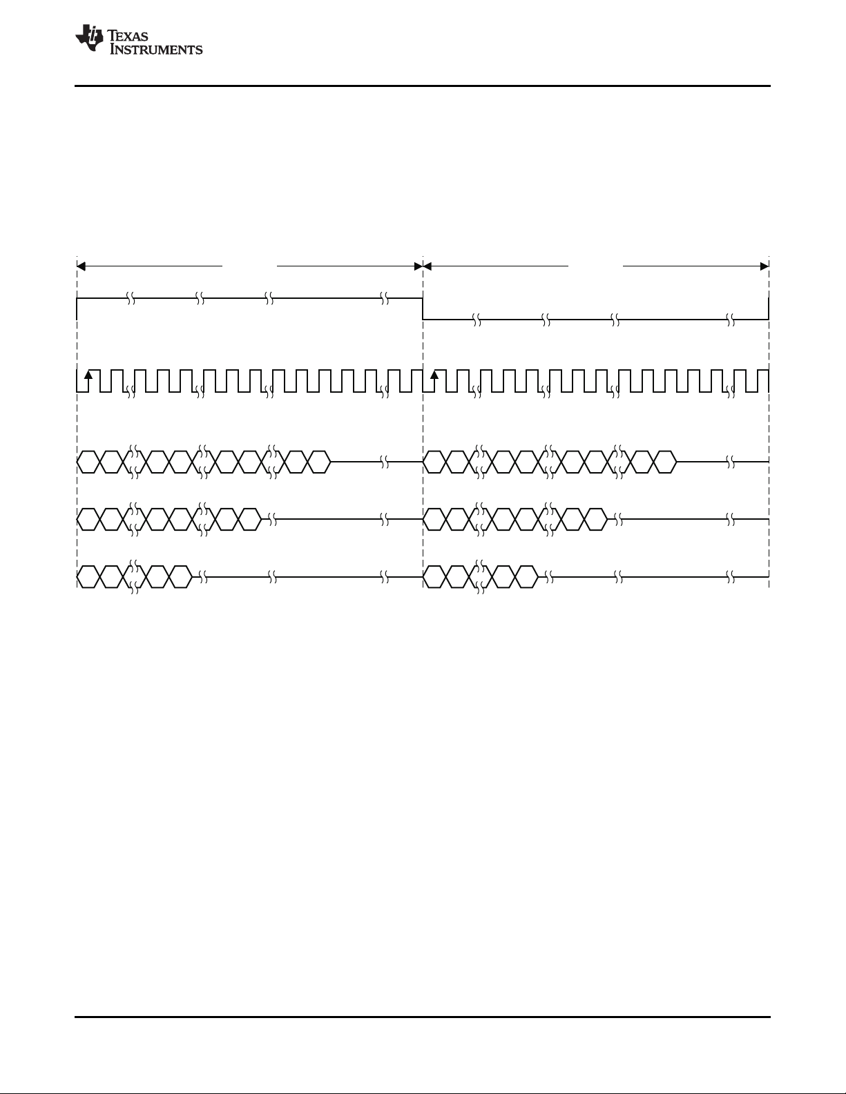
23
22
SCLK
32Clks
LRCLK
LeftChannel
24-BitMode
1
19 18
20-BitMode
16-BitMode
15
14
MSB LSB
32Clks
RightChannel
2-ChannelLeft-JustifiedStereoInput
T0034-02
4
5
9 8
1
4
5
1
0
0
0
23
22 1
19 18
15
14
MSB LSB
4
5
9 8
1
4
5
1
0
0
0
SCLK
TAS5508C
www.ti.com
SLES257–SEPTEMBER 2010
4.8.2 Left-Justified Timing
Left-justified (LJ) timing uses LRCLK to define when the data being transmitted is for the left channel and when it
is for the right channel. LRCLK is high for the left channel and low for the right channel. A bit clock running at 64
× Fs is used to clock in the data. The first bit of data appears on the data lines at the same time LRCLK toggles.
The data is written MSB first and is valid on the rising edge of the bit clock. The TAS5508C masks unused
trailing data bit positions.
Figure 4-10. Left-Justified 64-Fs Format
Copyright © 2010, Texas Instruments Incorporated Electrical Specifications 63
Submit Documentation Feedback
Product Folder Link(s): TAS5508C
Page 64

23
22
SCLK
32Clks
LRCLK
LeftChannel
24-BitMode
1
20-BitMode
16-BitMode
15
14
MSB LSB
SCLK
32Clks
RightChannel
2-ChannelRight-Justified(SonyFormat)StereoInput
T0034-03
19 18
1
19 18
1
0
0
0
15
14
15
14
23
22 1
15
14
MSB LSB
19 18
1
19 18
1
0
0
0
15
14
15
14
TAS5508C
SLES257–SEPTEMBER 2010
www.ti.com
4.8.3 Right-Justified Timing
Right-justified (RJ) timing uses LRCLK to define when the data being transmitted is for the left channel and when
it is for the right channel. LRCLK is high for the left channel and low for the right channel. A bit clock running at
64 × Fs is used to clock in the data. The first bit of data appears on the data lines eight bit-clock periods (for
24-bit data) after LRCLK toggles. In RJ mode the LSB of data is always clocked by the last bit clock before
LRCLK transitions. The data is written MSB first and is valid on the rising edge of the bit clock. The TAS5508C
masks unused leading data bit positions.
Figure 4-11. Right-Justified 64-Fs Format
64 Electrical Specifications Copyright © 2010, Texas Instruments Incorporated
Submit Documentation Feedback
Product Folder Link(s): TAS5508C
Page 65

7-BitSlave Address
R/
W
8-BitRegister Address(N)
A
8-BitRegisterDataFor
Address(N)
Start Stop
SDA
SCL
7
6
5
4
3
2 1
0
7
6
5
4
3
2 1
0
7
6
5
4
3
2 1
0
7
6
5
4
3
2 1
0
A
8-BitRegisterDataFor
Address(N)
A A
T0035-01
TAS5508C
www.ti.com
5 I2C Serial-Control Interface (Slave Address 0x36)
The TAS5508C has a bidirectional I2C interface that is compatible with the Inter-IC (I2C) bus protocol and
supports both 100-kbps and 400-kbps data transfer rates for single- and multiple-byte write and read
operations. This is a slave-only device that does not support a multimaster bus environment or wait state
insertion. The control interface is used to program the registers of the device and to read device status.
The TAS5508C supports the standard-mode I2C bus operation (100 kHz maximum) and the fast I2C bus
operation (400 kHz maximum). The TAS5508C performs all I2C operations without I2C wait cycles.
5.1 General I2C Operation
The I2C bus employs two signals—SDA (data) and SCL (clock)—to communicate between integrated
circuits in a system. Data is transferred on the bus serially, one bit at a time. The address and data can be
transferred in byte (8-bit) format, with the most significant bit (MSB) transferred first. In addition, each byte
transferred on the bus is acknowledged by the receiving device with an acknowledge bit. Each transfer
operation begins with the master device driving a start condition on the bus and ends with the master
device driving a stop condition on the bus. The bus uses transitions on SDA while the clock is high to
indicate start and stop conditions. A high-to-low transition on SDA indicates a start and a low-to-high
transition indicates a stop. Normal data bit transitions must occur within the low time of the clock period.
These conditions are shown in Figure 5-1. The master generates the 7-bit slave address and the
read/write (R/W) bit to open communication with another device and then wait for an acknowledge
condition. The TAS5508C holds SDA low during the acknowledge clock period to indicate an
acknowledgement. When this occurs, the master transmits the next byte of the sequence. Each device is
addressed by a unique 7-bit slave address plus R/W bit (1 byte). All compatible devices share the same
signals via a bidirectional bus using a wired-AND connection. An external pullup resistor must be used for
the SDA and SCL signals to set the high level for the bus.
SLES257–SEPTEMBER 2010
Figure 5-1. Typical I2C Sequence
There is no limit on the number of bytes that can be transmitted between start and stop conditions. When
the last word transfers, the master generates a stop condition to release the bus. A generic data transfer
sequence is shown in Figure 5-1.
The 7-bit address for the TAS5508C is 0011011.
5.2 Single- and Multiple-Byte Transfers
The serial-control interface supports both single-byte and multiple-byte read/write operations for status
registers and the general control registers associated with the PWM. However, for the DAP data
processing registers, the serial-control interface supports only multiple-byte (four-byte) read/write
operations.
During multiple-byte read operations, the TAS5508C responds with data, a byte at a time, starting at the
subaddress assigned, as long as the master device continues to respond with acknowledges. If a
particular subaddress does not contain 32 bits, the unused bits are read as logic 0.
Copyright © 2010, Texas Instruments Incorporated 65
Submit Documentation Feedback
Product Folder Link(s): TAS5508C
I2C Serial-Control Interface (Slave Address 0x36)
Page 66

A6 A5 A4 A3 A2 A1 A0
R/W
ACK A7 A6 A5 A4 A3 A2 A1 A0 ACK D7 D6 D5 D4 D3 D2 D1 D0 ACK
Start
Condition
Stop
Condition
Acknowledge Acknowledge Acknowledge
I CDevice Addressand
Read/WriteBit
2
Subaddress DataByte
T0481-01
D7 D0 ACK
Stop
Condition
Acknowledge
I CDevice Addressand
Read/WriteBit
2
Subaddress LastDataByte
A6 A5 A1 A0 R/W ACK A7 A5 A1 A0 ACK D7 ACK
Start
Condition
Acknowledge Acknowledge Acknowledge
FirstDataByte
A4 A3A6
OtherDataBytes
ACK
Acknowledge
D0 D7 D0
T0482-01
TAS5508C
SLES257–SEPTEMBER 2010
During multiple-byte write operations, the TAS5508C compares the number of bytes transmitted to the
number of bytes that are required for each specific subaddress. If a write command is received for a
biquad subaddress, the TAS5508C expects to receive five 32-bit words. If fewer than five 32-bit data
words have been received when a stop command (or another start command) is received, the data
received is discarded. Similarly, if a write command is received for a mixer coefficient, the TAS5508C
expects to receive one 32-bit word.
Supplying a subaddress for each subaddress transaction is referred to as random I2C addressing. The
TAS5508C also supports sequential I2C addressing. For write transactions, if a subaddress is issued
followed by data for that subaddress and the 15 subaddresses that follow, a sequential I2C write
transaction has taken place, and the data for all 16 subaddresses is successfully received by the
TAS5508C. For I2C sequential write transactions, the subaddress then serves as the start address and the
amount of data subsequently transmitted, before a stop or start is transmitted, determines how many
subaddresses are written. As is true for random addressing, sequential addressing requires that a
complete set of data be transmitted. If only a partial set of data is written to the last subaddress, the data
for the last subaddress is discarded. However, all other data written is accepted; only the incomplete data
is discarded.
5.3 Single-Byte Write
As shown in Figure 5-2, a single-byte, data-write transfer begins with the master device transmitting a start
condition followed by the I2C device address and the read/write bit. The read/write bit determines the
direction of the data transfer. For a write data transfer, the read/write bit is a 0. After receiving the correct
I2C device address and the read/write bit, the TAS5508C device responds with an acknowledge bit. Next,
the master transmits the address byte or bytes corresponding to the TAS5508C internal memory address
being accessed. After receiving the address byte, the TAS5508C again responds with an acknowledge bit.
Next, the master device transmits the data byte to be written to the memory address being accessed. After
receiving the data byte, the TAS5508C again responds with an acknowledge bit. Finally, the master
device transmits a stop condition to complete the single-byte, data-write transfer.
www.ti.com
Figure 5-2. Single-Byte Write Transfer
5.4 Multiple-Byte Write
A multiple-byte, data-write transfer is identical to a single-byte, data-write transfer except that multiple data
bytes are transmitted by the master device to TAS5508C, as shown in Figure 5-3. After receiving each
data byte, the TAS5508C responds with an acknowledge bit.
Figure 5-3. Multiple-Byte Write Transfer
66 Copyright © 2010, Texas Instruments Incorporated
I2C Serial-Control Interface (Slave Address 0x36)
Submit Documentation Feedback
Product Folder Link(s): TAS5508C
Page 67

A6 A5 A0 R/W ACK A7 A6 A5 A4 A0 ACK A6 A5 A0 ACK
Start
Condition
Stop
Condition
Acknowledge Acknowledge Acknowledge
I CDevice Addressand
Read/WriteBit
2
Subaddress DataByte
D7 D6 D1 D0 ACK
I CDevice Addressand
Read/WriteBit
2
Not
Acknowledge
R/WA1 A1
RepeatStart
Condition
T0483-01
TAS5508C
www.ti.com
5.5 Incremental Multiple-Byte Write
The I2C supports a special mode which permits I2C write operations to be broken up into multiple data
write operations that are multiples of four data bytes. These are 6-byte, 10-byte, 14-byte, 18-byte, etc.,
write operations that are composed of a device address, read/write bit, subaddress, and any multiple of
four bytes of data. This permits the system to write large register values incrementally without blocking
other I2C transactions.
This feature is enabled by the append subaddress function in the TAS5508C. This function enables the
TAS5508C to append four bytes of data to a register that was opened by a previous I2C register write
operation but has not received its complete number of data bytes. Because the length of the long registers
is a multiple of four bytes, using four-byte transfers has only an integral number of append operations.
When the correct number of bytes has been received, the TAS5508C starts processing the data.
The procedure to perform an incremental multibyte-write operation is as follows:
1. Start a normal I2C write operation by sending the device address, write bit, register subaddress, and
the first four bytes of the data to be written. At the end of that sequence, send a stop condition. At this
point, the register has been opened and accepts the remaining data that is sent by writing four-byte
blocks of data to the append subaddress (0xFE).
2. At a later time, one or more append data transfers are performed to incrementally transfer the
remaining number of bytes in sequential order to complete the register write operation. Each of these
append operations is composed of the device address, write bit, append subaddress (0xFE), and four
bytes of data followed by a stop condition.
3. The operation is terminated due to an error condition, and the data is flushed:
(a) If a new subaddress is written to the TAS5508C before the correct number of bytes are written.
(b) If more or fewer than four bytes are data written at the beginning or during any of the append
operations.
(c) If a read bit is sent.
SLES257–SEPTEMBER 2010
5.6 Single-Byte Read
As shown in Figure 5-4, a single-byte, data-read transfer begins with the master device transmitting a start
condition followed by the I2C device address and the read/write bit. For the data-read transfer, both a write
and then a read are actually performed. Initially, a write is performed to transfer the address byte or bytes
of the internal memory address to be read. As a result, the read/write bit is a 0. After receiving the
TAS5508C address and the read/write bit, the TAS5508C responds with an acknowledge bit. In addition,
after sending the internal memory address byte or bytes, the master device transmits another start
condition followed by the TAS5508C address and the read/write bit again. This time the read/write bit is a
1, indicating a read transfer. After receiving the TAS5508C and the read/write bit the TAS5508C again
responds with an acknowledge bit. Next, the TAS5508C transmits the data byte from the memory address
being read. After receiving the data byte, the master device transmits a not acknowledge followed by a
stop condition to complete the single-byte, data-read transfer.
Figure 5-4. Single-Byte Read Transfer
Copyright © 2010, Texas Instruments Incorporated 67
Submit Documentation Feedback
Product Folder Link(s): TAS5508C
I2C Serial-Control Interface (Slave Address 0x36)
Page 68
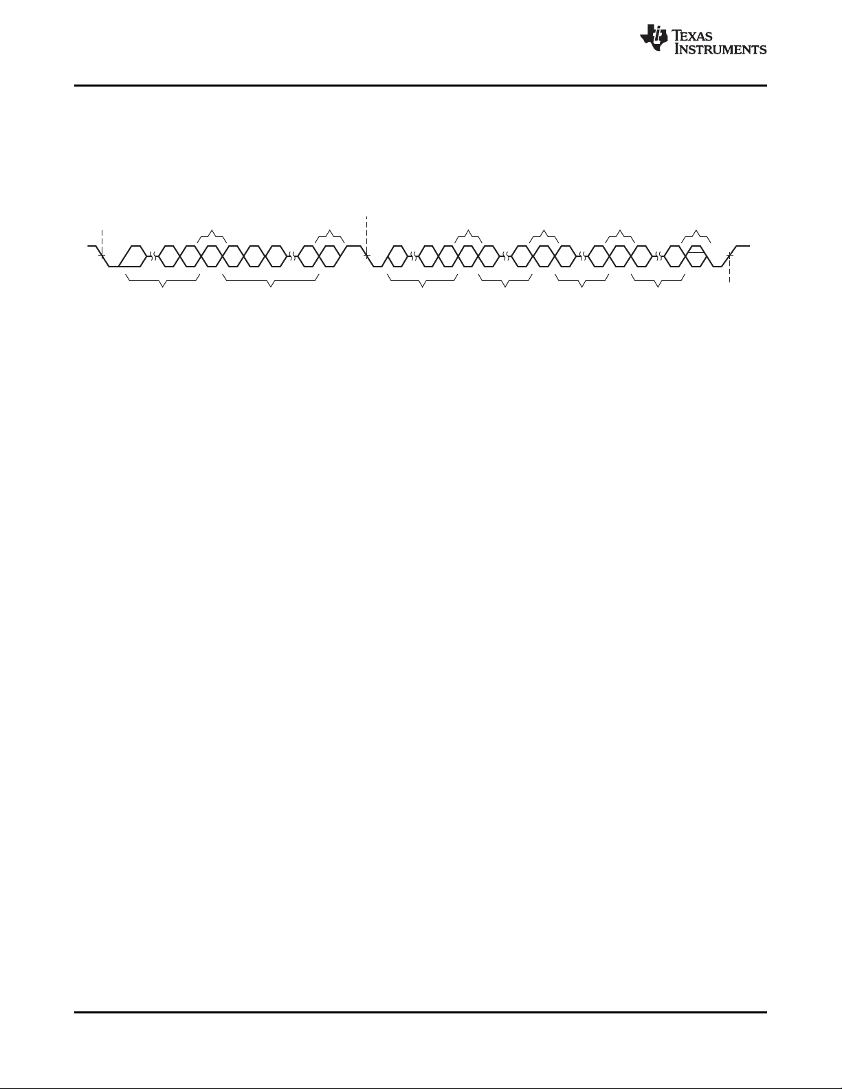
A6 A0 ACK
Acknowledge
I CDevice Addressand
Read/WriteBit
2
R/WA6 A0 R/W ACK A0 ACK D7 D0 ACK
Start
Condition
Stop
Condition
Acknowledge Acknowledge Acknowledge
LastDataByte
ACK
FirstDataByte
RepeatStart
Condition
Not
Acknowledge
I CDevice Addressand
Read/WriteBit
2
Subaddress OtherDataBytes
A7 A6 A5 D7 D0 ACK
Acknowledge
D7 D0
T0484-01
TAS5508C
SLES257–SEPTEMBER 2010
5.7 Multiple-Byte Read
A multiple-byte, data-read transfer is identical to a single-byte, data-read transfer except that multiple data
bytes are transmitted by the TAS5508C to the master device, as shown in Figure 5-5. Except for the last
data byte, the master device responds with an acknowledge bit after receiving each data byte.
www.ti.com
Figure 5-5. Multiple-Byte Read Transfer
68 Copyright © 2010, Texas Instruments Incorporated
I2C Serial-Control Interface (Slave Address 0x36)
Submit Documentation Feedback
Product Folder Link(s): TAS5508C
Page 69

TAS5508C
www.ti.com
SLES257–SEPTEMBER 2010
6 Serial-Control I2C Register Summary
The TAS5508C slave address is 0x36. See Serial-Control Interface Register Definitions, Section 7 for
complete bit definitions.
Note that u indicates unused bits.
I2C
SUBADDRESS
0x00 1 Clock control register Set data rate and MCLK frequency 1. Fs = 48 kHz
0x01 1 General status register Clip indicator and ID code for the 0x01
0x02 1 Error status register PLL, SCLK, LRCLK, and frame slip No errors
0x03 1 System control register 1
0x04 1 System control register 2 Automute and de-emphasis control 3. 8-Ch device input detection automute enabled
0x05–0x0C 1/reg. 4. Normal BEPolarity
0x0D 1 Configure headphone output 4. Normal BEPolarity
0x0E 1 Serial data interface control Set serial data interface to
0x0F 1 Soft mute register Soft mute for channels 1, 2, 3, 4, 5, 6, Unmute all channels.
0x10–0x13 Reserved
0x14 1 Automute control register Set automute delay and threshold. 1. Set automute delay = 5 ms.
0x15 1 Automute PWM threshold Set PWM automute threshold; set 1. Set the PWM threshold the same as the
0x16 1 Modulation index limit Set modulation index. 97.7%
0x17–0x1A Reserved
0x1B–0x22 1/reg. Interchannel delay registers Set interchannel delay.
0x23 1 Channel offset register Absolute delay offset for channel 1 Minimum absolute default = 0 DCLK periods
0x24–0x3F Reserved
0x40 4 Bank-switching command Set up DAP coefficients bank Manual selection – bank 1
TOTAL
BYTES
REGISTER FIELDS DESCRIPTION OF CONTENTS DEFAULT STATE
2. MCLK = 256 Fs = 12.288 MHz
TAS5508C
errors
PWM high pass, clock set, unmute 2. Auto clock set
select, PSVC select 3. Hard unmute on clock error recovery
Channel configuration Configure channels 1, 2, 3, 4, 5, 6, 7,
control registers and 8
Headphone configuration
control register
register
and back-end reset period back-end reset period. TAS5508C input threshold.
register 2. Set back-end reset period = 5 ms.
register
register switching for banks 1, 2, and 3
right-justified, I2S, or left-justified.
7, and 8
(0–255)
1. PWM high pass disabled
4. PSVC Hi-Z disabled
1. Automute time-out disabled
2. Post-DAP detection automute enabled
4. Unmute threshold 6 dB over input
5. No de-emphasis
1. Enable back-end reset.
2. Valid low for reset
3. Valid low for mute
5. Do not remap the output for the TAS5182.
6. Do not go low-low in mute.
7. Do not remap Hi-Z state to low-low state.
1. Disable back-end reset sequence.
2. Valid does not have to be low for reset.
3. Valid does not have to be low for mute.
5. Do not remap output to comply with 5182.
6. Do not go low-low in mute.
7. Do not remap Hi-Z state to low-low state.
24-bit I2S
2. Set automute threshold less than bit 8.
Channel 1 delay = –23 DCLK periods
Channel 2 delay = 0 DCLK periods
Channel 3 delay = –16 DCLK periods
Channel 4 delay = 16 DCLK periods
Channel 5 delay = –24 DCLK periods
Channel 6 delay = 8 DCLK periods
Channel 7 delay = –8 DCLK periods
Channel 8 delay = 24 DCLK periods
Copyright © 2010, Texas Instruments Incorporated 69
Serial-Control I2C Register Summary
Submit Documentation Feedback
Product Folder Link(s): TAS5508C
Page 70

TAS5508C
SLES257–SEPTEMBER 2010
I2C
SUBADDRESS
0x41–0x48 32/reg. 8×8 input crossbar mixer setup
0x49 4 ipmix_1_to_ch8 Input mixer 1 to Ch8 mixer coefficient 0.0
0x4A 4 ipmix_2_to_ch8 Input mixer 1 to Ch8 mixer coefficient 0.0
0x4B 4 ipmix_7_to_ch2 Input mixer 7 to Ch2 mixer coefficient 0.0
0x4C 4 Ch7_bp_bq2 Bypass Ch7 biquad 2 coefficient 0.0
0x4D 4 Ch7_bq2 Ch7 biquad 2 coefficient 1.0
0x4E 4 ipmix_8_to_ch12 Ch8 biquad 2 output to Ch1 mixer and 0.0
0x4F 4 Ch8_bp_bq2 Bypass Ch8 biquad 2 coefficient 0 0.0
0x50 4 Ch8_bq2 Ch8 biquad 2 coefficient 1.0
0x51–0x88 20/reg. Biquad filter register Ch1–Ch8 biquad filter coefficients All biquads = All pass for all channels
0x89–0x90 8 Bass and treble bypass Bypass bass and treble for Ch1–Ch8 Bassand treble bypassed for all channels
0x91 4 Loudness Log2 LG Loudness Log2 LG 0.5
0x92 8 Loudness Log2 LO Loudness Log2 LO 0.0
0x93 4 Loudness G Loudness G 0.0
0x94 8 Loudness O Loudness O 0.0
0x95 20 Loudness biquad Loudness biquad coefficient b2 0x0F, 0xFF, 0x2A, 0xED
0x96 4 DRC1 control Ch1–Ch7 DRC1 control Ch1–Ch7 DRC1 disabled in Ch1–Ch7
0x97 4 DRC2 control register, Ch8 DRC2 control Ch8 DRC2 disabled in Ch8
0x98 8
0x99 16
0x9A 12 Ch1–Ch7, DRC1 slope k1 DRC1 slope (k1) 0x0F, 0xC0, 0x00, 0x00
0x9B 16
0x9C 16
0x9D 8
0x9E 16
TOTAL
BYTES
REGISTER FIELDS DESCRIPTION OF CONTENTS DEFAULT STATE
SDIN1 – left to input mixer 1
SDIN1 – right to input mixer 2
Input mixer registers, SDIN2 – right to input mixer 4
Ch1–Ch8 SDIN3 – left to input mixer 5
Ch2 mixer coefficient
register, Ch1–Ch8
Loudness biquad coefficient b0 0x00, 0x00, 0xD5, 0x13
Loudness biquad coefficient b1 0x00, 0x00, 0x00, 0x00
Loudness biquad coefficient a0 0x00, 0xFE, 0x50, 0x45
Loudness biquad coefficient a1 0x0F, 0x81, 0xAA, 0x27
Ch1–Ch7, DRC1 energy DRC1 energy 0.0041579
Ch1–Ch7, DRC1 (1 – DRC1 (1 – energy) 0.9958421
energy)
Ch1–Ch7 DRC1 threshold DRC1 threshold (T1) – upper 2 bytes 0x00,0x00, 0x00, 0x00
T1
Ch1–Ch7 DRC1 threshold DRC1 threshold (T2) – upper 2 bytes 0x00,0x00, 0x00, 0x00
T2
Ch1–Ch7 , DRC1 slope k0 DRC1 slope (k0) 0x0F, 0xC0, 0x00, 0x00
Ch1–Ch7 DRC1 slope k2 DRC1 slope (k2) 0x0F, 0x90, 0x00, 0x00
Ch1–Ch7 DRC1 offset 1 DRC1 offset 1 (O1) – upper 2 bytes 0x00, 0x00, 0xFF, 0xFF
Ch1–Ch7 DRC1 offset 2 DRC1 offset 2 (O2) – upper 2 bytes 0x00, 0x00, 0x00, 0x00
Ch1–Ch7 DRC1 attack DRC1 attack 0x00, 0x00, 0x88, 0x3F
Ch1–Ch7 DRC1 (1 – attack) DRC1 (1 – attack) 0x00, 0x7F, 0x77, 0xC0
Ch1–Ch7 DRC1 decay DRC1 decay 0x00, 0x00, 0x00, 0xAE
Ch1–Ch7 DRC1 (1 – decay) DRC1 (1 – decay) 0x00, 0x7F, 0xFF, 0x51
Ch8 DRC2 energy DRC2 energy 0x00, 0x00, 0x88, 0x3F
Ch8 DRC2 (1 – energy) DRC2 (1 – energy) 0x00, 0x7F, 0x77, 0xC0
Ch8 DRC2 threshold T1
Ch8 DRC2 threshold T2
DRC1 threshold (T1) – lower 4 bytes 0x0B, 0x20, 0xE2, 0xB2
DRC1 threshold (T2) – lower 4 bytes 0x06, 0xF9, 0xDE, 0x58
DRC1 offset 1 (O1) – lower 4 bytes 0xFF, 0x82, 0x30, 0x98
DRC1 offset 2 (O2) – lower 4 bytes 0x01, 0x95, 0xB2, 0xC0
DRC2 threshold (T1) – upper 2 bytes 0x00, 0x00, 0x00, 0x00
DRC2 threshold (T1) – lower 4 bytes 0x0B, 0x20, 0xE2, 0xB2
DRC2 threshold (T2) – upper 2 bytes 0x00, 0x00, 0x00, 0x00
DRC2 threshold (T2) – lower 4 bytes 0x06, 0xF9, 0xDE, 0x58
SDIN2 – left to input mixer 3
SDIN3 – right to input mixer 6
SDIN4 – left to input mixer 7
SDIN4 – right to input mixer 8
www.ti.com
70 Copyright © 2010, Texas Instruments Incorporated
Serial-Control I2C Register Summary
Submit Documentation Feedback
Product Folder Link(s): TAS5508C
Page 71

TAS5508C
www.ti.com
I2C
SUBADDRESS
0x9F 12 Ch8 DRC2 slope k1 DRC2 slope (k1) 0x0F, 0xC0, 0x00, 0x00
0xA0 16
0xA1 16
0xA2 8
0xA3 8
0xA4 8
0xA5 8
0xA6 8
0xA7 8
0xA8 8
0xA9 8
0xAA 8 sel op1–8 and mix to PWM1 Select 0 to 2 of eight channels to Mix channels to PWM1
0xAB 8 sel op1–8 and mix to PWM2 Select 0 to 2 of eight channels to Mix channels to PWM2
0xAC 8 sel op1–8 and mix to PWM3 Select 0 to 2 of eight channels to Mix channels to PWM3
0xAD 8 sel op1–8 and mix to PWM4 Select 0 to 2 of eight channels to Mix channels to PWM4
0xAE 8 sel op1–8 and mix to PWM5 Select 0 to 2 of eight channels to Mix channels to PWM5
0xAF 8 sel op1–8 and mix to PWM6 Select 0 to 2 of eight channels to Mix channels to PWM6
0xB0 12 sel op1–8 and mix to PWM7 Select 0 to 3 of eight channels to Mix channels to PWM7
0xB1 12 sel op1–8 and mix to PWM8 Select 0 to 3 of eight channels to Mix channels to PWM8
0xB2–0xCE Reserved
0xCF 20 Volume biquad Volume biquad All pass
0xD0 4 Volume, treble, and bass u [31:24], u [23:16], u [15:12] 0x00, 0x00, 0x02, 0x3F
0xD1 4 Ch1 volume Ch1 volume 0 dB
0xD2 4 Ch2 volume Ch2 volume 0 dB
0xD3 4 Ch3 volume Ch3 volume 0 dB
0xD4 4 Ch4 volume Ch4 volume 0 dB
0xD5 4 Ch5 volume Ch5 volume 0 dB
0xD6 4 Ch6 volume Ch6 volume 0 dB
0xD7 4 Ch7 volume Ch7 volume 0 dB
0xD8 4 Ch8 volume Ch8 volume 0 dB
TOTAL
BYTES
REGISTER FIELDS DESCRIPTION OF CONTENTS DEFAULT STATE
Ch8 DRC2 slope k0 DRC2 slope (k0) 0x00, 0x40, 0x00, 0x00
Ch8 DRC2 slope k2 DRC2 slope (k2) 0x0F, 0x90, 0x00, 0x00
Ch8 DRC2 offset 1
Ch8 DRC2 offset 2
Ch8 DRC2 attack DRC 2 attack 0x00, 0x00, 0x88, 0x3F
Ch8 DRC2 (1 – attack) DRC2 (1 – attack) 0x00, 0x7F, 0x77, 0xC0
Ch8 DRC2 decay DRC2 decay 0x00, 0x00, 0x00, 0xAE
Ch8 DRC2 (1 – decay) DRC2 (1 – decay) 0x00, 0x7F, 0xFF, 0x51
DRC bypass 1 Ch1 DRC1 bypass coefficient 1.0
DRC inline 1 Ch1 DRC1 inline coefficient 0.0
DRC bypass 2 Ch2 DRC1 bypass coefficient 1.0
DRC inline 2 Ch2 DRC1 inline coefficient 0.0
DRC bypass 3 Ch3 DRC1 bypass coefficient 1.0
DRC inline 3 Ch3 DRC1 inline coefficient 0.0
DRC bypass 4 Ch4 DRC1 bypass coefficient 1.0
DRC inline 4 Ch4 DRC1 inline coefficient 0.0
DRC bypass 5 Ch5 DRC1 bypass coefficient 1.0
DRC inline 5 Ch5 DRC1 inline coefficient 0.0
DRC bypass 6 Ch6 DRC1 bypass coefficient 1.0
DRC inline 6 Ch6 DRC1 inline coefficient 0.0
DRC bypass 7 Ch7 DRC1 bypass coefficient 1.0
DRC inline 7 Ch7 DRC1 inline coefficient 0.0
DRC bypass 8 Ch8 DRC2 bypass coefficient 1.0
DRC inline 8 Ch8 DRC2 inline coefficient 0.0
slew rates register VSR[11:8], TBSR[7:0]
DRC2 offset (O1) – upper 2 bytes 0x00, 0x00, 0xFF, 0xFF
DRC2 offset (O1) – lower 4 bytes 0xFF, 0x82, 0x30, 0x98
DRC2 offset (O2) – upper 2 bytes 0x00, 0x00, 0x00, 0x00
DRC2 offset (O2) – lower 4 bytes 0x01, 0x95, 0xB2, 0xC0
output mixer 1
output mixer 2
output mixer 3
output mixer 4
output mixer 5
output mixer 6
output mixer 7
output mixer 8
SLES257–SEPTEMBER 2010
Copyright © 2010, Texas Instruments Incorporated 71
Serial-Control I2C Register Summary
Submit Documentation Feedback
Product Folder Link(s): TAS5508C
Page 72

TAS5508C
SLES257–SEPTEMBER 2010
I2C
SUBADDRESS
0xD9 4 Master volume Master volume Mute
0xDA 4 Bass filter set register Bass filter set (all channels) Filter set 3
0xDB 4 Bass filter index register Bass filter level (all channels) 0 dB
0xDC 4 Treble filter set register Treble filter set (all channels) Filter set 3
0xDD 4 Treble filter index register Treble filter level (all channels) 0 dB
0xDE 4 AM mode register Set up AM mode for AM-interference AM mode disabled
0xDF 4 PSVC range register Set PSVC control range 12-dB control range
0xE0 4 General control register 6- or 8-channel configuration, PSVC 8-channel configuration
0xE1–0xFD Reserved
0xFE 4 (min) Multiple-byte write-append Special register N/A
0xFF Reserved
TOTAL
BYTES
REGISTER FIELDS DESCRIPTION OF CONTENTS DEFAULT STATE
reduction Select sequence 1
IF frequency = 455 kHz
Use BCD-tuned frequency
enable Power-supply volume control disabled
register
www.ti.com
72 Copyright © 2010, Texas Instruments Incorporated
Serial-Control I2C Register Summary
Submit Documentation Feedback
Product Folder Link(s): TAS5508C
Page 73

TAS5508C
www.ti.com
7 Serial-Control Interface Register Definitions
Unless otherwise noted, the I2C register default values are in bold font.
Note that u indicates unused bits.
7.1 Clock Control Register (0x00)
Bit D1 is Don't Care.
Table 7-1. Clock Control Register Format
D7 D6 D5 D4 D3 D2 D1 D0 FUNCTION
0 0 0 – – – – 32-kHz data rate
0 0 1 – – – – 38-kHz data rate
0 1 0 – – – – 44.1-kHz data rate
0 1 1 – – – – 48-kHz data rate
1 0 0 – – – – 88.2-kHz data rate
1 0 1 – – – – 96-kHz data rate
1 1 0 – – – – 176.4-kHz data rate
1 1 1 – – – – 192-kHz data rate
– – – 0 0 0 MCLK frequency = 64
– – – 0 0 1 MCLK frequency = 128
– – – 0 1 0 MCLK frequency = 192
– – – 0 1 1 MCLK frequency = 256
– – – 1 0 0 MCLK frequency = 384
– – – 1 0 1 MCLK frequency = 512
– – – 1 1 0 MCLK frequency = 768
– – – 1 1 1 Reserved
– – – – – – 1 Clock register is valid (read-only)
– – – – – – 0 Clock register is not valid (read-only)
SLES257–SEPTEMBER 2010
7.2 General Status Register 0 (0x01)
Table 7-2. General Status Register Format
D7 D6 D5 D4 D3 D2 D1 D0 FUNCTION
1 – – – – – – – Clip indicator
– 1 – – – – – – Bank switching busy
– – 0 0 0 0 0 1 Identification code for TAS5508C
Copyright © 2010, Texas Instruments Incorporated Serial-Control Interface Register Definitions 73
Submit Documentation Feedback
Product Folder Link(s): TAS5508C
Page 74
TAS5508C
SLES257–SEPTEMBER 2010
7.3 Error Status Register (0x02)
Note that the error bits are sticky bits that are not cleared by the hardware. This means that the software
must clear the register (write zeroes) and then read them to determine if there are any persistent errors.
Table 7-3. Error Status Register Format
D7 D6 D5 D4 D3 D2 D1 D0 FUNCTION
1 – – – – – – – PLL phase lock error
– 1 – – – – – – PLL auto lock error
– – 1 – – – – – SCLK error
– – – 1 – – – – LRCLK error
– – – – 1 – – – Frame slip
0 0 0 0 0 0 0 0 No errors
7.4 System Control Register 1 (0x03)
Bits D5, D2, D1, and D0 are Don't Care.
Table 7-4. System Control Register 1 Format
D7 D6 D5 D4 D3 D2 D1 D0 Function
0 – – – PWM high pass disabled
1 – – – PWM high pass enabled
– – 0 Soft unmute on recovery from clock error
– – 1 Hard unmute on recovery from clock error
– – – 1 PSVC Hi-Z enable
– – – 0 PSVC Hi-Z disable
www.ti.com
7.5 System Control Register 2 (0x04)
Bits D3 and D2 are Don't Care.
Table 7-5. System Control Register 2 Format
D7 D6 D5 D4 D3 D2 D1 D0 Function
0 – – – – – Reserved
– 0 – – – – PWM automute detection enabled
– 1 – – – – PWM automute detection disabled
0 – – – 8-Ch device input detection automute enabled
– – 1 – – – 8-Ch device input detection automute disabled
– – – 0 – – Unmute threshold 6 dB over input threshold
– – – 1 – – Unmute threshold equal to input threshold
– – – – 0 0 No de-emphasis
– – – – 0 1 De-emphasis for Fs = 32 kHz
– – – – 1 0 De-emphasis for Fs = 44.1 kHz
– – – – 1 1 De-emphasis for Fs = 48 kHz
7.6 Channel Configuration Control Registers (0x05–0x0C)
Channels 1, 2, 3, 4, 5, 6, 7, and 8 are mapped into 0x05, 0x06, 0x07, 0x08, 0x09, 0x0A, 0x0B, and 0x0C,
respectively.
Bit D0 is Don't Care.
74 Serial-Control Interface Register Definitions Copyright © 2010, Texas Instruments Incorporated
Submit Documentation Feedback
Product Folder Link(s): TAS5508C
Page 75
TAS5508C
www.ti.com
SLES257–SEPTEMBER 2010
Table 7-6. Channel Configuration Control Register Format
D7 D6 D5 D4 D3 D2 D1 D0 FUNCTION
0 – – – – – – Disable back-end reset sequence for a channel – BEErrorRecEn
1 – – – – – – Enable back-end reset sequence for a channel
– 0 – – – – – Valid does not have to be low for this channel to be reset BEValidRst
– 1 – – – – – Valid must be low for this channel to be reset
– – 0 – – – – Valid does not have to be low for this channel to be muted BEValidMute
– – 1 – – – – Valid must be low for this channel to be muted
– – – 0 – – – Normal BEPolarity
– – – 1 – – – Switches PWM+ and PWM– and inverts audio signal
– – – – 0 – – Do not remap output to comply with 5182 interface
– – – – 1 – – Remap output to comply with 5182 interface
– – – – – 0 – Do not go to low-low in mute – BELowMute
– – – – – 1 – Go to low-low in mute
– – – – – – 0 Do not remap Hi-Z state to low-low state – BE5111BsMute
– – – – – – 1 Remap Hi-Z state to low-low state
7.7 Headphone Configuration Control Register (0x0D)
Bit D0 is Don't Care.
Table 7-7. Headphone Configuration Control Register Format
D7 D6 D5 D4 D3 D2 D1 D0 FUNCTION
0 – – – – – – Disable back-end reset sequence for a channel – BEErrorRecEn
1 – – – – – – Enable back-end reset sequence for a channel
– 0 – – – – – Valid does not have to be low for this channel to be reset
– 1 – – – – – Valid must be low for this channel to be reset
– – 0 – – – – Valid does not have to be low for this channel to be muted
– – 1 – – – – Valid must be low for this channel to be muted
– – – 0 – – – Normal BEPolarity
– – – 1 – – – Switches PWM+ and PWM– and inverts audio signal
– – – – 0 – – Do not remap output to comply with 5182 interface
– – – – 1 – – Remap output to comply with 5182 interface
– – – – – 0 – Do not go to low-low in mute – BELowMute
– – – – – 1 – Go to low-low in mute
– – – – – – 0 Do not remap Hi-Z state to low-low state – BE5111BsMute
– – – – – – 1 Remap Hi-Z state to low-low state
BEValidRst
BEValidMute
7.8 Serial Data Interface Control Register (0x0E)
Nine serial modes can be programmed via the I2C interface.
Table 7-8. Serial Data Interface Control Register Format
RECEIVE SERIAL DATA
INTERFACE FORMAT
Right-justified 16 0000 0 0 0 0
Right-justified 20 0000 0 0 0 1
Right-justified 24 0000 0 0 1 0
Copyright © 2010, Texas Instruments Incorporated Serial-Control Interface Register Definitions 75
WORD LENGTHS D7–D4 D3 D2 D1 D0
Submit Documentation Feedback
Product Folder Link(s): TAS5508C
Page 76

TAS5508C
SLES257–SEPTEMBER 2010
Table 7-8. Serial Data Interface Control Register Format (continued)
RECEIVE SERIAL DATA
INTERFACE FORMAT
I2S 16 0000 0 0 1 1
I2S 20 0000 0 1 0 0
I2S 24 0000 0 1 0 1
Left-justified 16 0000 0 1 1 0
Left-justified 20 0000 0 1 1 1
Left-justified 24 0000 1 0 0 0
Reserved 0000 1 0 0 1
Reserved 0000 1 0 1 0
Reserved 0000 1 0 1 1
Reserved 0000 1 1 0 0
Reserved 0000 1 1 0 1
Reserved 0000 1 1 1 0
Reserved 0000 1 1 1 1
7.9 Soft Mute Register (0x0F)
www.ti.com
WORD LENGTHS D7–D4 D3 D2 D1 D0
Table 7-9. Soft Mute Register Format
D7 D6 D5 D4 D3 D2 D1 D0 FUNCTION
– – – – – – – 1 Soft mute channel 1
– – – – – – 1 – Soft mute channel 2
– – – – – 1 – – Soft mute channel 3
– – – – 1 – – – Soft mute channel 4
– – – 1 – – – – Soft mute channel 5
– – 1 – – – – – Soft mute channel 6
– 1 – – – – – – Soft mute channel 7
1 – – – – – – – Soft mute channel 8
0 0 0 0 0 0 0 0 Unmute All Channels
76 Serial-Control Interface Register Definitions Copyright © 2010, Texas Instruments Incorporated
Submit Documentation Feedback
Product Folder Link(s): TAS5508C
Page 77
TAS5508C
www.ti.com
SLES257–SEPTEMBER 2010
7.10 Automute Control Register (0x14)
Table 7-10. Automute Control Register Format
D7 D6 D5 D4 D3 D2 D1 D0 FUNCTION
– – – – 0 0 0 0 Set input automute and PWM automute delay to 1 ms
– – – – 0 0 0 1 Set input automute and PWM automute delay to 2 ms
– – – – 0 0 1 0 Set input automute and PWM automute delay to 3 ms
– – – – 0 0 1 1 Set input automute and PWM automute delay to 4 ms
– – – – 0 1 0 0 Set input automute and PWM automute delay to 5 ms
– – – – 0 1 0 1 Set input automute and PWM automute delay to 10 ms
– – – – 0 1 1 0 Set input automute and PWM automute delay to 20 ms
– – – – 0 1 1 1 Set input automute and PWM automute delay to 30 ms
– – – – 1 0 0 0 Set input automute and PWM automute delay to 40 ms
– – – – 1 0 0 1 Set input automute and PWM automute delay to 50 ms
– – – – 1 0 1 0 Set input automute and PWM automute delay to 60 ms
– – – – 1 0 1 1 Set input automute and PWM automute delay to 70ms
– – – – 1 1 0 0 Set input automute and PWM automute delay to 80 ms
– – – – 1 1 0 1 Set input automute and PWM automute delay to 90 ms
– – – – 1 1 1 0 Set input automute and PWM automute delay to 100 ms
– – – – 1 1 1 1 Set input automute and PWM automute delay to 110 ms
0 0 0 0 – – –
0 0 0 1 – – – –
0 0 1 0 – – – – Set input automute threshold less than bit 2
0 0 1 1 – – – – Set input automute threshold less than bit 3
0 1 0 0 – – – – Set input automute threshold less than bit 4
0 1 0 1 – – – – Set input automute threshold less than bit 5
0 1 1 0 – – – – Set input automute threshold less than bit 6
0 1 1 1 – – – – Set input automute threshold less than bit 7
1 0 0 0 – – – – Set input automute threshold less than bit 8
1 0 0 1 – – – – Set input automute threshold less than bit 9
1 0 1 0 – – – – Set input automute threshold less than bit 10
1 0 1 1 – – – – Set input automute threshold less than bit 11
1 1 0 0 – – – – Set input automute threshold less than bit 12
1 1 0 1 – – – – Set input automute threshold less than bit 13
1 1 1 0 – – – – Set input automute threshold less than bit 14
1 1 1 1 – – – – Set input automute threshold less than bit 15
Set input automute threshold less than bit 1 (zero input signal), lowest
automute threshold.
Copyright © 2010, Texas Instruments Incorporated Serial-Control Interface Register Definitions 77
Submit Documentation Feedback
Product Folder Link(s): TAS5508C
Page 78
TAS5508C
SLES257–SEPTEMBER 2010
7.11 Automute PWM Threshold and Back-End Reset Period Register (0x15)
Table 7-11. Automute PWM Threshold and Back-End Reset Period Register Format
D7 D6 D5 D4 D3 D2 D1 D0 FUNCTION
0 0 0 0 – – – – Set PWM automute threshold equal to input automute threshold
0 0 0 1 – – – – Set PWM automute threshold 1 bit more than input automute threshold
0 0 1 0 – – – – Set PWM automute threshold 2 bits more than input automute threshold
0 0 1 1 – – – – Set PWM automute threshold 3 bits more than input automute threshold
0 1 0 0 – – – – Set PWM automute threshold 4 bits more than input automute threshold
0 1 0 1 – – – – Set PWM automute threshold 5 bits more than input automute threshold
0 1 1 0 – – – – Set PWM automute threshold 6 bits more than input automute threshold
0 1 1 1 – – – – Set PWM automute threshold 7 bits more than input automute threshold
1 0 0 0 – – – – Set PWM automute threshold equal to input automute threshold
1 0 0 1 – – – – Set PWM automute threshold 1 bit less than input automute threshold
1 0 1 0 – – – – Set PWM automute threshold 2 bits less than input automute threshold
1 0 1 1 – – – – Set PWM automute threshold 3 bits less than input automute threshold
1 1 0 0 – – – – Set PWM automute threshold 4 bits less than input automute threshold
1 1 0 1 – – – – Set PWM automute threshold 5 bits less than input automute threshold
1 1 1 0 – – – – Set PWM automute threshold 6 bits less than input automute threshold
1 1 1 1 – – – – Set PWM automute threshold 7 bits less than input automute threshold
– – – – 0 0 0 0 Set back-end reset period < 1 ms
– – – – 0 0 0 1 Set back-end reset period 1 ms
– – – – 0 0 1 0 Set back-end reset period 2 ms
– – – – 0 0 1 1 Set back-end reset period 3 ms
– – – – 0 1 0 0 Set back-end reset period 4 ms
– – – – 0 1 0 1 Set back-end reset period 5 ms
– – – – 0 1 1 0 Set back-end reset period 6 ms
– – – – 0 1 1 1 Set back-end reset period 7 ms
– – – – 1 0 0 0 Set back-end reset period 8 ms
– – – – 1 0 0 1 Set back-end reset period 9 ms
– – – – 1 0 1 0 Set back-end reset period 10 ms
– – – – 1 0 1 1 Set back-end reset period 10 ms
– – – – 1 1 X X Set back-end reset period 10 ms
www.ti.com
78 Serial-Control Interface Register Definitions Copyright © 2010, Texas Instruments Incorporated
Submit Documentation Feedback
Product Folder Link(s): TAS5508C
Page 79
TAS5508C
www.ti.com
7.12 Modulation Index Limit Register (0x16)
Bits D7–D3 are Don't Care.
Table 7-12. Modulation Index Limit Register Format
D7 D6 D5 D4 D3 D2 D1 D0
0 0 0 1 2 99.2%
0 0 1 2 4 98.4%
0 1 0 3 6 97.7%
0 1 1 4 8 96.9%
1 0 0 5 10 96.1%
1 0 1 6 12 95.3%
1 1 0 7 14 94.5%
1 1 1 8 16 93.8%
7.13 Interchannel Delay Registers (0x1B–0x22)
Channels 1, 2, 3, 4, 5, 6, 7, and 8 are mapped into 0x1B, 0x1C, 0x1D, 0x1E, 0x1F, 0x20, 0x21, and 0x22,
respectively.
Bits D1 and D0 are Don't Care.
SLES257–SEPTEMBER 2010
LIMIT MIN WIDTH MODULATION
[DCLKs] [DCLKs] INDEX
Table 7-13. Interchannel Delay Register Format
D7 D6 D5 D4 D3 D2 D1 D0 FUNCTION
0 0 0 0 0 0 Minimum absolute delay, 0 DCLK cycles, default for channel 1
0 1 1 1 1 1 Maximum positive delay, 31 × 4 DCLK cycles
1 0 0 0 0 0 Maximum negative delay, –32 × 4 DCLK cycles
1 0 0 0 0 0 Default value for channel 1 = –32
0 0 0 0 0 0 Default value for channel 2 = 0
1 1 0 0 0 0 Default value for channel 3 = –16
0 1 0 0 0 0 Default value for channel 4 = 16
1 0 1 0 0 0 Default value for channel 5 = –24
0 0 1 0 0 0 Default value for channel 6 = 8
1 1 1 0 0 0 Default value for channel 7 = –8
0 1 1 0 0 0 Default value for channel 8 = 24
7.14 Channel Offset Register (0x23)
The channel offset register is mapped into 0x23.
Table 7-14. Channel Offset Register Format
D7 D6 D5 D4 D3 D2 D1 D0 Function
0 0 0 0 0 0 0 0 Minimum absolute offset, 0 DCLK cycles, default for channel 1
1 1 1 1 1 1 1 1 Maximum absolute offset, 255 DCLK cycles
Copyright © 2010, Texas Instruments Incorporated Serial-Control Interface Register Definitions 79
Submit Documentation Feedback
Product Folder Link(s): TAS5508C
Page 80

TAS5508C
SLES257–SEPTEMBER 2010
7.15 Bank-Switching Command Register (0x40)
Bits D31–D24, D22–D19 are Don't Care.
Table 7-15. Bank-Switching Command Register Format
D31 D30 D29 D28 D27 D26 D25 D24 FUNCTION
Unused bits
D23 D22 D21 D20 D19 D18 D17 D16 FUNCTION
– 0 0 0 Manual selection bank 1
– 0 0 1 Manual selection bank 2
– 0 1 0 Manual selection bank 3
– 0 1 1 Automatic bank selection
– 1 0 0 Update the values in bank 1
– 1 0 1 Update the values in bank 2
– 1 1 0 Update the values in bank 3
– 1 1 1 Update only the bank map
0 x x x Update the bank map using values in D15–D0
1 x x x Do not update the bank map using values in D15–D0
D15 D14 D13 D12 D11 D10 D9 D8 FUNCTION
1 – – – – – – – 32-kHz data rate—use bank 1
– 1 – – – – – – 38-kHz data rate—use bank 1
– – 1 – – – – – 44.1-kHz data rate—use bank 1
– – – 1 – – – – 48-kHz data rate—use bank 1
– – – – 1 – – – 88.2-kHz data rate—use bank 1
– – – – – 1 – – 96-kHz data rate—use bank 1
– – – – – – 1 – 176.4-kHz data rate—use bank 1
– – – – – – – 1 192-kHz data rate—use bank 1
1 1 1 1 1 1 1 1 Default
www.ti.com
D7 D6 D5 D4 D3 D2 D1 D0 FUNCTION
1 – – – – – – – 32-kHz data rate—use bank 2
– 1 – – – – – – 38-kHz data rate—use bank 2
– – 1 – – – – – 44.1-kHz data rate—use bank 2
– – – 1 – – – – 48-kHz data rate—use bank 2
– – – – 1 – – – 88.2-kHz data rate—use bank 2
– – – – – 1 – – 96-kHz data rate—use bank 2
– – – – – – 1 – 176.4-kHz data rate—use bank 2
– – – – – – – 1 192-kHz data rate—use bank 2
1 1 1 1 1 1 1 1 Default
7.16 Input Mixer Registers, Channels 1–8 (0x41–0x48)
Input mixers 1, 2, 3, 4, 5, 6, 7, and 8 are mapped into registers 0x41, 0x42, 0x43, 0x44, 0x45, 0x46, 0x47,
and 0x48, respectively.
Each gain coefficient is in 28-bit (5.23) format so 0x80 0000 is a gain of 1. Each gain coefficient is written
as a 32-bit word with the upper four bits not used. For 8-gain coefficients, the total is 32 bytes.
Bold indicates the one channel that is passed through the mixer.
80 Serial-Control Interface Register Definitions Copyright © 2010, Texas Instruments Incorporated
Submit Documentation Feedback
Product Folder Link(s): TAS5508C
Page 81

TAS5508C
www.ti.com
Table 7-16. Channel 1–8 Input Mixer Register Format
I2C TOTAL REGISTER
SUBADDRESS BYTES FIELDS
A_to_ipmix[1]
B_to_ipmix[1]
C_to_ipmix[1]
D_to_ipmix[1]
0x41 32
E_to_ipmix[1]
F_to_ipmix[1]
G_to_ipmix[1]
H_to_ipmix[1]
A_to_ipmix[2]
B_to_ipmix[2]
C_to_ipmix[2]
D_to_ipmix[2]
0x42 32
E_to_ipmix[2]
F_to_ipmix[2]
G_to_ipmix[2]
H_to_ipmix[2]
A_to_ipmix[3]
B_to_ipmix[3]
C_to_ipmix[3]
D_to_ipmix[3]
0x43 32
E_to_ipmix[3]
F_to_ipmix[3]
G_to_ipmix[3]
H_to_ipmix[3]
SLES257–SEPTEMBER 2010
DESCRIPTION OF CONTENTS DEFAULT STATE
SDIN1-left (Ch1) A to input mixer 1 coefficient (default = 1) 0x00, 0x80, 0x00, 0x00
u[31:28], A_1[27:24], A_1[23:16], A_1[15:8], A_1[7:0]
SDIN1-right (Ch2) B to input mixer 1 coefficient (default = 0) 0x00, 0x00, 0x00, 0x00
u[31:28], B_1[27:24], B_1[23:16], B_1[15:8], B_1[7:0]
SDIN2-left (Ch3) C to input mixer 1 coefficient (default = 0) 0x00, 0x00, 0x00, 0x00
u[31:28], C_1[27:24], C_1[23:16], C_1[15:8], C_1[7:0]
SDIN2-right (Ch4) D to input mixer 1 coefficient (default = 0) 0x00, 0x00, 0x00, 0x00
u[31:28], D_1[27:24], D_1[23:16], D_1[15:8], D_1[7:0]
SDIN3-left (Ch5) E to input mixer 1 coefficient (default = 0) 0x00, 0x00, 0x00, 0x00
u[31:28], E_1[27:24], E_1[23:16], E_1[15:8], E_1[7:0]
SDIN3-right (Ch6) F to input mixer 1 coefficient (default = 0) 0x00, 0x00, 0x00, 0x00
u[31:28], F_1[27:24], F_1[23:16], F_1[15:8], F_1[7:0]
SDIN4-left (Ch7) G to input mixer 1 coefficient (default = 0) 0x00, 0x00, 0x00, 0x00
u[31:28], G_1[27:24], G_1[23:16], G_1[15:8], G_1[7:0]
SDIN4-right (Ch8) H to input mixer 1 coefficient (default = 0) 0x00, 0x00, 0x00, 0x00
u[31:28], H_1[27:24], H_1[23:16], H_1[15:8], H_1[7:0]
SDIN1-left (Ch1) A to input mixer 2 coefficient (default = 0) 0x00, 0x00, 0x00, 0x00
u[31:28], A_2[27:24], A_2[23:16], A_2[15:8], A_2[7:0]
SDIN1-right (Ch2) B to input mixer 2 coefficient (default = 1) 0x00, 0x80, 0x00, 0x00
u[31:28], B_2[27:24], B_2[23:16], B_2[15:8], B_2[7:0]
SDIN2-left (Ch3) C to input mixer 2 coefficient (default = 0) 0x00, 0x00, 0x00, 0x00
u[31:28], C_2[27:24], C_2[23:16], C_2[15:8], C_2[7:0]
SDIN2-right (Ch4) D to input mixer 2 coefficient (default = 0) 0x00, 0x00, 0x00, 0x00
u[31:28], D_2[27:24], D_2[23:16], D_2[15:8], D_2[7:0]
SDIN3-left (Ch5) E to input mixer 2 coefficient (default = 0) 0x00, 0x00, 0x00, 0x00
u[31:28], E_2[27:24], E_2[23:16], E_2[15:8], E_2[7:0]
SDIN3-right (Ch6) F to input mixer 2 coefficient (default = 0) 0x00, 0x00, 0x00, 0x00
u[31:28], F_2[27:24], F_2[23:16], F_2[15:8], F_2[7:0]
SDIN4-left (Ch7) G to input mixer 2 coefficient (default = 0) 0x00, 0x00, 0x00, 0x00
u[31:28], G_2[27:24], G_2[23:16], G_2[15:8], G_2[7:0]
SDIN4-right (Ch8) H to input mixer 2 coefficient (default = 0) 0x00, 0x00, 0x00, 0x00
u[31:28], H_2[27:24], H_2[23:16], H_2[15:8], H_2[7:0]
SDIN1-left (Ch1) A to input mixer 3 coefficient (default = 0) 0x00, 0x00, 0x00, 0x00
u[31:28], A_3[27:24], A_3[23:16], A_3[15:8], A_3[7:0]
SDIN1-right (Ch2) B to input mixer 3 coefficient (default = 0) 0x00, 0x00, 0x00, 0x00
u[31:28], B_3[27:24], B_3[23:16], B_3[15:8], B_3[7:0]
SDIN2-left (Ch3) C to input mixer 3 coefficient (default = 1) 0x00, 0x80, 0x00, 0x00
u[31:28], C_3[27:24], C_3[23:16], C_3[15:8], C_3[7:0]
SDIN2-right (Ch4) D to input mixer 3 coefficient (default = 0) 0x00, 0x00, 0x00, 0x00
u[31:28], D_3[27:24], D_3[23:16], D_3[15:8], D_3[7:0]
SDIN3-left (Ch5) E to input mixer 3 coefficient (default = 0) 0x00, 0x00, 0x00, 0x00
u[31:28], E_3[27:24], E_3[23:16], E_3[15:8], E_3[7:0]
SDIN3-right (Ch6) F to input mixer 3 coefficient (default = 0) 0x00, 0x00, 0x00, 0x00
u[31:28], F_3[27:24], F_3[23:16], F_3[15:8], F_3[7:0]
SDIN4-left (Ch7) G to input mixer 3 coefficient (default = 0) 0x00, 0x00, 0x00, 0x00
u[31:28], G_3[27:24], G_3[23:16], G_3[15:8], G_3[7:0]
SDIN4-right (Ch8) H to input mixer 3 coefficient (default = 0) 0x00, 0x00, 0x00, 0x00
u[31:28], H_3[27:24], H_3[23:16], H_3[15:8], H_3[7:0]
Copyright © 2010, Texas Instruments Incorporated Serial-Control Interface Register Definitions 81
Submit Documentation Feedback
Product Folder Link(s): TAS5508C
Page 82

TAS5508C
SLES257–SEPTEMBER 2010
Table 7-16. Channel 1–8 Input Mixer Register Format (continued)
I2C TOTAL REGISTER
SUBADDRESS BYTES FIELDS
A_to_ipmix[4]
B_to_ipmix[4]
C_to_ipmix[4]
D_to_ipmix[4]
0x44 32
E_to_ipmix[4]
F_to_ipmix[4]
G_to_ipmix[4]
H_to_ipmix[4]
A_to_ipmix[5]
B_to_ipmix[5]
C_to_ipmix[5]
D_to_ipmix[5]
0x45 32
E_to_ipmix[5]
F_to_ipmix[5]
G_to_ipmix[5]
H_to_ipmix[5]
A_to_ipmix[6]
B_to_ipmix[6]
C_to_ipmix[6]
D_to_ipmix[6]
0x46 32
E_to_ipmix[6]
F_to_ipmix[6]
G_to_ipmix[6]
H_to_ipmix[6]
www.ti.com
DESCRIPTION OF CONTENTS DEFAULT STATE
SDIN1-left (Ch1) A to input mixer 4 coefficient (default = 0) 0x00, 0x00, 0x00, 0x00
u[31:28], A_4[27:24], A_4[23:16], A_4[15:8], A_4[7:0]
SDIN1-right (Ch2) B to input mixer 4 coefficient (default = 0) 0x00, 0x00, 0x00, 0x00
u[31:28], B_4[27:24], B_4[23:16], B_4[15:8], B_4[7:0]
SDIN2-left (Ch3) C to input mixer 4 coefficient (default = 0) 0x00, 0x00, 0x00, 0x00
u[31:28], C_4[27:24], C_4[23:16], C_4[15:8], C_4[7:0]
SDIN2-right (Ch4) D to input mixer 4 coefficient (default = 1) 0x00, 0x80, 0x00, 0x00
u[31:28], D_4[27:24], D_4[23:16], D_4[15:8], D_4[7:0]
SDIN3-left (Ch5) E to input mixer 4 coefficient (default = 0) 0x00, 0x00, 0x00, 0x00
u[31:28], E_4[27:24], E_4[23:16], E_4[15:8], E_4[7:0]
SDIN3-right (Ch6) F to input mixer 4 coefficient (default = 0) 0x00, 0x00, 0x00, 0x00
u[31:28], F_4[27:24], F_4[23:16], F_4[15:8], F_4[7:0]
SDIN4-left (Ch7) G to input mixer 4 coefficient (default = 0) 0x00, 0x00, 0x00, 0x00
u[31:28], G_4[27:24], G_4[23:16], G_4[15:8], G_4[7:0]
SDIN4-right (Ch8) H to input mixer 4 coefficient (default = 0) 0x00, 0x00, 0x00, 0x00
u[31:28], H_4[27:24], H_4[23:16], H_4[15:8], H_4[7:0]
SDIN1-left (Ch1) A to input mixer 5 coefficient (default = 0) 0x00, 0x00, 0x00, 0x00
u[31:28], A_5[27:24], A_5[23:16], A_5[15:8], A_5[7:0]
SDIN1-right (Ch2) B to input mixer 5 coefficient (default = 0) 0x00, 0x00, 0x00, 0x00
u[31:28], B_5[27:24], B_5[23:16], B_5[15:8], B_5[7:0]
SDIN2-left (Ch3) C to input mixer 5 coefficient (default = 0) 0x00, 0x00, 0x00, 0x00
u[31:28], C_5[27:24], C_5[23:16], C_5[15:8], C_5[7:0]
SDIN2-right (Ch4) D to input mixer 5 coefficient (default = 0) 0x00, 0x00, 0x00, 0x00
u[31:28], D_5[27:24], D_5[23:16], D_5[15:8], D_5[7:0]
SDIN3-left (Ch5) E to input mixer 5 coefficient (default = 1) 0x00, 0x80, 0x00, 0x00
u[31:28], E_5[27:24], E_5[23:16], E_5[15:8], E_5[7:0]
SDIN3-right (Ch6) F to input mixer 5 coefficient (default = 0) 0x00, 0x00, 0x00, 0x00
u[31:28], F_5[27:24], F_5[23:16], F_5[15:8], F_5[7:0]
SDIN4-left (Ch7) G to input mixer 5 coefficient (default = 0) 0x00, 0x00, 0x00, 0x00
u[31:28], G_5[27:24], G_5[23:16], G_5[15:8], G_5[7:0]
SDIN4-right (Ch8) H to input mixer 5 coefficient (default = 0) 0x00, 0x00, 0x00, 0x00
u[31:28], H_5[27:24], H_5[23:16], H_5[15:8], H_5[7:0]
SDIN1-left (Ch1) A to input mixer 6 coefficient (default = 0) 0x00, 0x00, 0x00, 0x00
u[31:28], A_6[27:24], A_6[23:16], A_6[15:8], A_6[7:0]
SDIN1-right (Ch2) B to input mixer 6 coefficient (default = 0) 0x00, 0x00, 0x00, 0x00
u[31:28], B_6[27:24], B_6[23:16], B_6[15:8], B_6[7:0]
SDIN2-left (Ch3) C to input mixer 6 coefficient (default = 0) 0x00, 0x00, 0x00, 0x00
u[31:28], C_6[27:24], C_6[23:16], C_6[15:8], C_6[7:0]
SDIN2-right (Ch4) D to input mixer 6 coefficient (default = 0) 0x00, 0x00, 0x00, 0x00
u[31:28], D_6[27:24], D_6[23:16], D_6[15:8], D_6[7:0]
SDIN3-left (Ch5) E to input mixer 6 coefficient (default = 0) 0x00, 0x00, 0x00, 0x00
u[31:28], E_6[27:24], E_6[23:16], E_6[15:8], E_6[7:0]
SDIN3-right (Ch6) F to input mixer 6 coefficient (default = 1) 0x00, 0x80, 0x00, 0x00
u[31:28], F_6[27:24], F_6[23:16], F_6[15:8], F_6[7:0]
SDIN4-left (Ch7) G to input mixer 6 coefficient (default = 0) 0x00, 0x00, 0x00, 0x00
u[31:28], G_6[27:24], G_6[23:16], G_6[15:8], G_6[7:0]
SDIN4-right (Ch8) H to input mixer 6 coefficient (default = 0) 0x00, 0x00, 0x00, 0x00
u[31:28], H_6[27:24], H_6[23:16], H_6[15:8], H_6[7:0]
82 Serial-Control Interface Register Definitions Copyright © 2010, Texas Instruments Incorporated
Submit Documentation Feedback
Product Folder Link(s): TAS5508C
Page 83

TAS5508C
www.ti.com
Table 7-16. Channel 1–8 Input Mixer Register Format (continued)
I2C TOTAL REGISTER
SUBADDRESS BYTES FIELDS
A_to_ipmix[7]
B_to_ipmix[7]
C_to_ipmix[7]
D_to_ipmix[7]
0x47 32
E_to_ipmix[7]
F_to_ipmix[7]
G_to_ipmix[7]
H_to_ipmix[7]
A_to_ipmix[8]
B_to_ipmix[8]
C_to_ipmix[8]
D_to_ipmix[8]
0x48 32
E_to_ipmix[8]
F_to_ipmix[8]
G_to_ipmix[8]
H_to_ipmix[8]
SLES257–SEPTEMBER 2010
DESCRIPTION OF CONTENTS DEFAULT STATE
SDIN1-left (Ch1) A to input mixer 7 coefficient (default = 0) 0x00, 0x00, 0x00, 0x00
u[31:28], A_7[27:24], A_7[23:16], A_7[15:8], A_7[7:0]
SDIN1-right (Ch2) B to input mixer 7 coefficient (default = 0) 0x00, 0x00, 0x00, 0x00
u[31:28], B_7[27:24], B_7[23:16], B_7[15:8], B_7[7:0]
SDIN2-left (Ch3) C to input mixer 7 coefficient (default = 0) 0x00, 0x00, 0x00, 0x00
u[31:28], C_7[27:24], C_7[23:16], C_7[15:8], C_7[7:0]
SDIN2-right (Ch4) D to input mixer 7 coefficient (default = 0) 0x00, 0x00, 0x00, 0x00
u[31:28], D_7[27:24], D_7[23:16], D_7[15:8], D_7[7:0]
SDIN3-left (Ch5) E to input mixer 7 coefficient (default = 0) 0x00, 0x00, 0x00, 0x00
u[31:28], E_7[27:24], E_7[23:16], E_7[15:8], E_7[7:0]
SDIN3-right (Ch6) F to input mixer 7 coefficient (default = 0) 0x00, 0x00, 0x00, 0x00
u[31:28], F_7[27:24], F_7[23:16], F_7[15:8], F_7[7:0]
SDIN4-left (Ch7) G to input mixer 7 coefficient (default = 1) 0x00, 0x80, 0x00, 0x00
u[31:28], G_7[27:24], G_7[23:16], G_7[15:8], G_7[7:0]
SDIN4-right (Ch8) H to input mixer 7 coefficient (default = 0) 0x00, 0x00, 0x00, 0x00
u[31:28], H_7[27:24], H_7[23:16], H_7[15:8], H_7[7:0]
SDIN1-left (Ch1) A to input mixer 8 coefficient (default = 0) 0x00, 0x00, 0x00, 0x00
u[31:28], A_8[27:24], A_8[23:16], A_8[15:8], A_8[7:0]
SDIN1-right (Ch2) B to input mixer 8 coefficient (default = 0) 0x00, 0x00, 0x00, 0x00
u[31:28], B_8[27:24], B_8[23:16], B_8[15:8], B_8[7:0]
SDIN2-left (Ch3) C to input mixer 8 coefficient (default = 0) 0x00, 0x00, 0x00, 0x00
u[31:28], C_8[27:24], C_8[23:16], C_8[15:8], C_8[7:0]
SDIN2-right (Ch4) D to input mixer 8 coefficient (default = 0) 0x00, 0x00, 0x00, 0x00
u[31:28], D_8[27:24], D_8[23:16], D_8[15:8], D_8[7:0]
SDIN3-left (Ch5) E to input mixer 8 coefficient (default = 0) 0x00, 0x00, 0x00, 0x00
u[31:28], E_8[27:24], E_8[23:16], E_8[15:8], E_8[7:0]
SDIN3-right (Ch6) F to input mixer 8 coefficient (default = 0) 0x00, 0x00, 0x00, 0x00
u[31:28], F_8[27:24], F_8[23:16], F_8[15:8], F_8[7:0]
SDIN4-left (Ch7) G to input mixer 8 coefficient (default = 0) 0x00, 0x00, 0x00, 0x00
u[31:28], G_8[27:24], G_8[23:16], G_8[15:8], G_8[7:0]
SDIN4-right (Ch8) H to input mixer 8 coefficient (default = 1) 0x00, 0x80, 0x00, 0x00
u[31:28], H_8[27:24], H_8[23:16], H_8[15:8], H_8[7:0]
Copyright © 2010, Texas Instruments Incorporated Serial-Control Interface Register Definitions 83
Submit Documentation Feedback
Product Folder Link(s): TAS5508C
Page 84

TAS5508C
SLES257–SEPTEMBER 2010
7.17 Bass Management Registers (0x49–0x50)
Registers 0x49–0x50 provide configuration control for bass mangement.
Each gain coefficient is in 28-bit (5.23) format so 0x80 0000 is a gain of 1. Each gain coefficient is written
as a 32-bit word with the upper four bits not used.
Table 7-17. Bass Management Register Format
SUB- TOTAL REGISTER
ADDRESS BYTES NAME
0x49 4 ipmix_1_to_ch8 Input mixer 1 to Ch8 mixer coefficient (default = 0) 0x00, 0x00, 0x00, 0x00
u[31:28], ipmix18[27:24], ipmix18[23:16], ipmix18[15:8],
ipmix18[7:0]
0x4A 4 ipmix_2_to_ch8 Input mixer 1 to Ch8 mixer coefficient (default = 0) 0x00, 0x00, 0x00, 0x00
u[31:28], ipmix28[27:24], ipmix28[23:16], ipmix28[15:8],
ipmix28[7:0]
0x4B 4 ipmix_7_to_ch12 Input mixer 7 to Ch1 and Ch2 mixer coefficient (default = 0) 0x00, 0x00, 0x00, 0x00
u[31:28], ipmix72[27:24], ipmix72[23:16], ipmix72[15:8],
ipmix72[7:0]
0x4C 4 Ch7_bp_bq2 Ch7 biquad-2 bypass coefficient (default = 0) 0x00, 0x00, 0x00, 0x00
u[31:28], ch7_bp_bq2[27:24], ch7_bp_bq2[23:16],
ch7_bp_bq2[15:8], ch7_bp_bq2[7:0]
0x4D 4 Ch7_bq2 Ch7 biquad-2 inline coefficient (default = 1) 0x00, 0x80, 0x00, 0x00
u[31:28], ch6_bq2[27:24], ch6_bq2[23:16], ch6_bq2[15:8],
ch6_bq2[7:0]
0x4E 4 ipmix_8_to_ch12 Ch8 biquad-2 output to Ch1 mixer and Ch2 mixer coefficient 0x00, 0x00, 0x00, 0x00
(default = 0)
u[31:28], ipmix8_12[27:24], ipmix8_12[23:16],
ipmix8_12[15:8], ipmix8_12[7:0]
0x4F 4 Ch8_bp_bq2 Ch8 biquad-2 bypass coefficient (default = 0) 0x00, 0x00, 0x00, 0x00
u[31:28], ch8_bp_bq2[27:24], ch8_bp_bq2[23:16],
ch8_bp_bq2[15:8], ch8_bp_bq2[7:0]
0x50 4 Ch8_bq2 Ch8 biquad-2 inline coefficient (default = 1) 0x00, 0x80, 0x00, 0x00
u[31:28], ch7_bq2[27:24], ch7_bq2[23:16], ch7_bq2[15:8],
ch7_bq2[7:0]
DESCRIPTION OF CONTENTS DEFAULT STATE
www.ti.com
7.18 Biquad Filter Register (0x51–0x88)
Table 7-18. Biquad Filter Register Format
I2C TOTAL REGISTER DEFAULT
SUBADDRESS BYTES NAME STATE
0x51–0x57 20/reg. Ch1_bq[1:7] Ch1 biquads 1–7. See Table 7-19 for bit definition. See Table 7-19
0x58–0x5E 20/reg. Ch2_bq[1:7] Ch2 biquads 1–7. See Table 7-19 for bit definition. See Table 7-19
0x5F–0x65 20/reg. Ch3_bq[1:7] Ch3 biquads 1–7. See Table 7-19 for bit definition. See Table 7-19
0x66–0x6C 20/reg. Ch4_bq[1:7] Ch4 biquads 1–7. See Table 7-19 for bit definition. See Table 7-19
0x6D–0x73 20/reg. Ch5_bq[1:7] Ch5 biquads 1–7. See Table 7-19 for bit definition. See Table 7-19
0x74–0x7A 20/reg. Ch6_bq[1:7] Ch6 biquads 1–7. See Table 7-19 for bit definition. See Table 7-19
0x7B–0x81 20/reg. Ch7_bq[1:7] Ch7 biquads 1–7. See Table 7-19 for bit definition. See Table 7-19
0x82–0x88 20/reg. Ch8_bq[1:7] Ch8 biquads 1–7. See Table 7-19 for bit definition. See Table 7-19
84 Serial-Control Interface Register Definitions Copyright © 2010, Texas Instruments Incorporated
Submit Documentation Feedback
Product Folder Link(s): TAS5508C
DESCRIPTION OF CONTENTS
Page 85

TAS5508C
www.ti.com
SLES257–SEPTEMBER 2010
Each gain coefficient is in 28-bit (5.23) format so 0x80 0000 is a gain of 1. Each gain coefficient is written
as a 32-bit word with the upper four bits not used.
Table 7-19. Contents of One 20-Byte Biquad Filter Register (Default = All-Pass)
DESCRIPTION REGISTER FIELD CONTENTS
b0coefficient u[31:28], b0[27:24], b0[23:16], b0[15:8], b0[7:0] 1.0 0x00, 0x80, 0x00, 0x00
b1coefficient u[31:28], b1[27:24], b1[23:16], b1[15:8], b1[7:0] 0.0 0x00, 0x00, 0x00, 0x00
b2coefficient u[31:28], b2[27:24], b2[23:16], b2[15:8], b2[7:0] 0.0 0x00, 0x00, 0x00, 0x00
a1coefficient u[31:28], a1[27:24], a1[23:16], a1[15:8], a1[7:0] 0.0 0x00, 0x00, 0x00, 0x00
a2coefficient u[31:28], a2[27:24], a2[23:16], a2[15:8], a2[7:0] 0.0 0x00, 0x00, 0x00, 0x00
DEFAULT GAIN COEFFICIENT VALUES
DECIMAL HEX
7.19 Bass and Treble Bypass Register, Channels 1–8 (0x89–0x90)
Channels 1, 2, 3, 4, 5, 6, 7, and 8 are mapped into registers 0x89, 0x8A, 0x8B, 0x8C, 0x8D, 0x8E, 0x8F,
and 0x90, respectively. Eight bytes are written for each channel. Each gain coefficient is in 28-bit (5.23)
format so 0x80 0000 is a gain of 1. Each gain coefficient is written as a 32-bit word with the upper four bits
not used.
Table 7-20. Channel 1–8 Bass and Treble Bypass Register Format
REGISTER TOTAL
NAME BYTES
Channel bass and u[31:28], bypass[27:24], bypass[23:16], bypass[15:8], bypass[7:0] 0x00, 0x80, 0x00, 0x00
treble bypass
Channel bass and u[31:28], inline[27:24], inline[23:16], inline[15:8], inline[7:0] 0x00, 0x00, 0x00, 0x00
treble inline
8
CONTENTS INITIALIZATION VALUE
7.20 Loudness Registers (0x91–0x95)
Table 7-21. Loudness Register Format
I2C SUB- TOTAL
ADDRESS BYTES
0x91 4 Loudness Log2 gain (LG) u[31:28], LG[27:24], LG[23:16], LG[15:8], LG[7:0] 0xFF, 0xC0, 0x00, 0x00
0x92 8
0x93 4 Loudness gain (G) u[31:28], G[27:24], G[23:16], G[15:8], G[7:0] 0x00, 0x00, 0x00, 0x00
0x94 8
0x95 20 Loudness biquad (b2) u[31:28], b2[27:24], b2[23:16], b2[15:8], b2[7:0] 0x0F, 0xFF, 0x2A, 0xED
REGISTER NAME DESCRIPTION OF CONTENTS DEFAULT STATE
Loudness Log2 offset (LO) u[31:24], u[23:16], LO[15:8], LO[7:0] 0x00, 0x00, 0x00, 0x00
Loudness Log2 LO LO[31:24], LO[23:16], LO[15:8], LO[7:0] 0x00, 0x00, 0x00, 0x00
Loudness offset upper u[31:24], u[23:16], O[15:8], O[7:0] 0x00, 0x00, 0x00, 0x00
16 bits (O)
Loudness O offset lower 32 O[31:24], O[23:16], O[15:8], O[7:0] 0x00, 0x00, 0x00, 0x00
bits (O)
Loudness biquad (b0) u[31:28], b0[27:24], b0[23:16], b0[15:8], b0[7:0] 0x00, 0x00, 0xD5, 0x13
Loudness biquad (b1) u[31:28], b1[27:24], b1[23:16], b1[15:8], b1[7:0] 0x00, 0x00, 0x00, 0x00
Loudness biquad (a1) u[31:28], a1[27:24], a1[23:16], a1[15:8], a1[7:0] 0x00, 0xFE, 0x50, 0x45
Loudness biquad (a2) u[31:28], a2[27:24], a2[23:16], a2[15:8], a2[7:0] 0x0F, 0x81, 0xAA, 0x27
Copyright © 2010, Texas Instruments Incorporated Serial-Control Interface Register Definitions 85
Submit Documentation Feedback
Product Folder Link(s): TAS5508C
Page 86

TAS5508C
SLES257–SEPTEMBER 2010
7.21 DRC1 Control Registers, Channels 1–7 (0x96)
Bits D31–D14 are Don't Care.
Table 7-22. Channel 1–7 DCR1 Control Register Format
D31 D30 D29 D28 D27 D26 D25 D24 FUNCTION
Unused bits
D23 D22 D21 D20 D19 D18 D17 D16 FUNCTION
Unused bits
D15 D14 D13 D12 D11 D10 D9 D8 FUNCTION
0 0 – – – – Channel 1 (node j): No DRC
0 1 – – – – Channel 1 (node j): Pre-volume DRC
1 0 – – – – Channel 1 (node j): Post-volume DRC
1 1 – – – – Channel 1 (node j): No DRC
– – 0 0 – – Channel 2 (node I): No DRC
– – 0 1 – – Channel 2 (node I): Pre-volume DRC
– – 1 0 – – Channel 2 (node I): Post-volume DRC
– – 1 1 – – Channel 2 (node i): No DRC
– – – – 0 0 Channel 3 (node m): No DRC
– – – – 0 1 Channel 3 (node m): Pre-volume DRC
– – – – 1 0 Channel 3 (node m): Post-volume DRC
– – – – 1 1 Channel 3 (node m): No DRC
www.ti.com
D7 D6 D5 D4 D3 D2 D1 D0 FUNCTION
0 0 – – – – – – Channel 4 (node n): No DRC
0 1 – – – – – – Channel 4 (node n): Pre-volume DRC
1 0 – – – – – – Channel 4 (node n): Post-volume DRC
1 1 – – – – – – Channel 4 (node n): No DRC
– – 0 0 – – – – Channel 5 (node o): No DRC
– – 0 1 – – – – Channel 5 (node o): Pre-volume DRC
– – 1 0 – – – – Channel 5 (node o): Post-volume DRC
– – 1 1 – – – – Channel 5 (node o): No DRC
– – – – 0 0 – – Channel 6 (node p): No DRC
– – – – 0 1 – – Channel 6 (node p): Pre-volume DRC
– – – – 1 0 – – Channel 6 (node p): Post-volume DRC
– – – – 1 1 – – Channel 6 (node p): No DRC
– – – – – – 0 0 Channel 7 (node q): No DRC
– – – – – – 0 1 Channel 7 (node q): Pre-volume DRC
– – – – – – 1 0 Channel 7 (node q): Post-volume DRC
– – – – – – 1 1 Channel 7 (node q): No DRC
86 Serial-Control Interface Register Definitions Copyright © 2010, Texas Instruments Incorporated
Submit Documentation Feedback
Product Folder Link(s): TAS5508C
Page 87

TAS5508C
www.ti.com
7.22 DRC2 Control Register, Channel 8 (0x97)
Table 7-23. Channel-8 DRC2 Control Register Format
D31–D2 D1 D0 FUNCTION
0 0 0 0 Channel 8 (node r): no DRC
0 0 0 1 Channel 8 (node r): pre-volume DRC
0 0 1 0 Channel 8 (node r): post-volume DRC
0 0 1 1 Channel 8 (node r): no DRC
7.23 DRC1 Data Registers (0x98–0x9C)
DRC1 applies to channels 1, 2, 3, 4, 5, 6, and 7.
Table 7-24. DRC1 Data Register Format
I2C
SUB-
ADDRESS
0x98 8
0x99 16
0x9A 12
0x9B 16
0x9C 16
TOTAL
BYTES
REGISTER NAME DESCRIPTION OF CONTENTS DEFAULT STATE
Channel 1, 2, 3, 4, 5, 6, and 7 DRC1 u[31:28], E[27:24], E[23:16], E[15:8], E[7:0] 0x00, 0x00, 0x88, 0x3F
energy
Channel 1, 2, 3, 4, 5, 6, and 7 DRC1 u[31:28], 1–E[27:24], 1–E[23:16], 1–E[15:8], 1–E[7:0] 0x00, 0x7F, 0x77, 0xC0
(1 – energy)
Channel 1, 2, 3, 4, 5, 6, and 7 DRC1 u[31:24], u[23:16], T1[15:8], T1[7:0] 0x00, 0x00, 0x00, 0x00
threshold upper 16 bits (T1)
Channel 1, 2, 3, 4, 5, 6, and 7 DRC1 T1[31:24], T1[23:16], T1[15:8], T1[7:0] 0x0B, 0x20, 0xE2, 0xB2
threshold lower 32 bits (T1)
Channel 1, 2, 3, 4, 5, 6, and 7 DRC1 u[31:24], u[23:16], T2[15:8], T2[7:0] 0x00, 0x00, 0x00, 0x00
threshold upper 16 bits (T2)
Channel 1, 2, 3, 4, 5, 6, and 7 DRC1 T2[31:24], T2[23:16], T2[15:8], T2[7:0] 0x06, 0xF9, 0xDE, 0x58
threshold lower 32 bits (T2)
Channel 1, 2, 3, 4, 5, 6, and 7 DRC1 u[31:28], k0[27:24], k0[23:16], k0[15:8], k0[7:0] 0x00, 0x40, 0x00, 0x00
slope (k0)
Channel 1, 2, 3, 4, 5, 6, and 7 DRC1 u[31:28], k1[27:24], k1[23:16], k1[15:8], k1[7:0] 0x0F, 0xC0, 0x00, 0x00
slope (k1)
Channel 1, 2, 3, 4, 5, 6, and 7 DRC1 u[31:28], k2[27:24], k2[23:16], k2[15:8], k2[7:0] 0x0F, 0x90, 0x00, 0x00
slope (k2)
Channel 1, 2, 3, 4, 5, 6, and 7 DRC1 u[31:24], u[23:16], O1[15:8], O1[7:0] 0x00, 0x00, 0xFF, 0xFF
offset 1 upper 16 bits (O1)
Channel 1, 2, 3, 4, 5, 6, and 7 DRC1 O1[31:24], O1[23:16], O1[15:8], O1[7:0] 0xFF, 0x82, 0x30, 0x98
offset 1 lower 32 bits (O1)
Channel 1, 2, 3, 4, 5, 6, and 7 DRC1 u[31:24], u[23:16], O2[15:8], O2[7:0] 0x00, 0x00, 0x00, 0x00
offset 2 upper 16 bits (O2)
Channel 1, 2, 3, 4, 5, 6, and 7 DRC1 O2[31:24], O2[23:16], O2[15:8], O2[7:0] 0x01, 0x95, 0xB2, 0xC0
offset 2 lower 32 bits (O2)
Channel 1, 2, 3, 4, 5, 6, and 7 DRC1 u[31:28], A[27:24], A[23:16], A[15:8], A[7:0] 0x00, 0x00, 0x88, 0x3F
attack
Channel 1, 2, 3, 4, 5, 6, and 7 DRC1 u[31:28], 1–A[27:24], 1–A[23:16], 1–A[15:8], 1–A[7:0] 0x00, 0x7F, 0x77, 0xC0
(1 – attack)
Channel 1, 2, 3, 4, 5, 6, and 7 DRC1 u[31:28], D[27:24], D[23:16], D[15:8], D[7:0] 0x00, 0x00, 0x00, 0x56
decay
Channel 1, 2, 3, 4, 5, 6, and 7 DRC1 u[31:28], 1–D[27:24], 1–D[23:16], 1–D[15:8], 1–D[7:0] 0x00, 0x3F, 0xFF, 0xA8
(1 – decay)
SLES257–SEPTEMBER 2010
Copyright © 2010, Texas Instruments Incorporated Serial-Control Interface Register Definitions 87
Submit Documentation Feedback
Product Folder Link(s): TAS5508C
Page 88

TAS5508C
SLES257–SEPTEMBER 2010
7.24 DRC2 Data Registers (0x9D–0xA1)
DRC2 applies to channel 8.
Table 7-25. DRC2 Data Register Format
I2C
SUBADDRESS
0x9D 8
0x9E 16
0x9F 12 Channel 8 DRC2 slope (k1) u[31:28], k1[27:24], k1[23:16], k1[15:8], k1[7:0] 0x0F, 0xC0, 0x00, 0x00
0xA0 16
0xA1 16
TOTAL
BYTES
REGISTER NAME DESCRIPTION OF CONTENTS DEFAULT STATE
Channel 8 DRC2 energy u[31:28], E[27:24], E[23:16], E[15:8], E[7:0] 0x00, 0x00, 0x88, 0x3F
Channel 8 DRC2 (1 – energy) u[31:28], 1–E[27:24], 1–E[23:16], 1–E[15:8], 1–E[7:0] 0x00, 0x7F, 0x77, 0xC0
Channel 8 DRC2 threshold u[31:24], u[23:16], T1[15:8], T1[7:0] 0x00, 0x00, 0x00, 0x00
upper 16 bits (T1)
Channel 8 DRC2 threshold T1[31:24], T1[23:16], T1[15:8], T1[7:0] 0x0B, 0x20, 0xE2, 0xB2
lower 32 bits (T1)
Channel 8 DRC2 threshold u[31:24], u[23:16], T2[15:8], T2[7:0] 0x00, 0x00, 0x00, 0x00
upper 16 bits (T2)
Channel 8 DRC2 threshold T2[31:24], T2[23:16], T2[15:8], T2[7:0] 0x06, 0xF9, 0xDE, 0x58
lower 32 bits (T2)
Channel 8 DRC2 slope (k0) u[31:28], k0[27:24], k0[23:16], k0[15:8], k0[7:0] 0x00, 0x40, 0x00, 0x00
Channel 8 DRC2 slope (k2) u[31:28], k2[27:24], k2[23:16], k2[15:8], k2[7:0] 0x0F, 0x90, 0x00, 0x00
Channel 8 DRC2 offset 1 upper u[31:24], u[23:16], O1[15:8], O1[7:0] 0x00, 0x00, 0xFF, 0xFF
16 bits (O1)
Channel 8 DRC2 offset 1 lower O1[31:24], O1[23:16], O1[15:8], O1[7:0] 0xFF, 0x82, 0x30, 0x98
32 bits (O1)
Channel 8 DRC2 offset 2 upper u[31:24], u[23:16], O2[15:8], O2[7:0] 0x00, 0x00, 0x00, 0x00
16 bits (O2)
Channel 8 DRC2 offset 2 lower O2[31:24], O2[23:16], O2[15:8], O2[7:0] 0x01, 0x95, 0xB2, 0xC0
32 bits (O2)
Channel 8 DRC2 attack u[31:28], A[27:24], A[23:16], A[15:8], A[7:0] 0x00, 0x00, 0x88, 0x3F
Channel 8 DRC2 (1 – attack) u[31:28], 1–A[27:24], 1–A[23:16], 1–A[15:8], 1–A[7:0] 0x00, 0x7F, 0x77, 0xC0
Channel 8 DRC2 decay u[31:28], D[27:24], D[23:16], D[15:8], D[7:0] 0x00, 0x00, 0x00, 0x56
Channel 8 DRC2 (1 – decay) u[31:28], 1–D[27:24], 1–D[23:16], 1–D[15:8], 1–D[7:0] 0x00, 0x3F, 0xFF, 0xA8
www.ti.com
7.25 DRC Bypass Registers (0xA2–0xA9)
DRC bypass/inline for channels 1, 2, 3, 4, 5, 6, 7, and 8 are mapped into registers 0xA2, 0xA3, 0xA4,
0xA5, 0xA6, 0xA7, 0xA8, and 0xA9, respectively. Eight bytes are written for each channel. Each gain
coefficient is in 28-bit (5.23) format, so 0x0080 0000 is a gain of 1. Each gain coefficient is written as a
32-bit word with the upper 4 bits not used.
To enable DRC for a given channel (with unity gain), bypass = 0x0000 0000 and inline = 0x0080 0000.
To disable DRC for a given channel, bypass = 0x00800000 and inline = 0x0000 0000.
Table 7-26. DRC Bypass Register Format
REGISTER NAME CONTENTS INITIALIZATION VALUE
Channel bass DRC bypass u[31:28], bypass[27:24], bypass[23:16], bypass[15:8], bypass[7:0] 0x00, 0x80, 0x00, 0x00
Channel DRC inline u[31:28], inline[27:24], inline[23:16], inline[15:8], inline[7:0] 0x00, 0x00, 0x00, 0x00
TOTAL
BYTES
8
7.26 8×2 Output Mixer Registers (0xAA–0xAF)
Output mixers for channels 1–6 map to registers 0xAA–0xAF.
Total data per register is 8 bytes.
88 Serial-Control Interface Register Definitions Copyright © 2010, Texas Instruments Incorporated
Submit Documentation Feedback
Product Folder Link(s): TAS5508C
Page 89

TAS5508C
www.ti.com
Table 7-27. Output Mixer Register Format (Upper 4 Bytes)
D31 D30 D29 D28 D27 D26 D25 D24 FUNCTION
0 0 0 0 Select channel 1 to output mixer
0 0 0 1 Select channel 2 to output mixer
0 0 1 0 Select channel 3 to output mixer
0 0 1 1 Select channel 4 to output mixer
0 1 0 0 Select channel 5 to output mixer
0 1 0 1 Select channel 6 to output mixer
0 1 1 0 Select channel 7 to output mixer
0 1 1 1 Select channel 8 to output mixer
G27 G26 G25 G24 Selected channel gain (upper 4 bits)
D23 D22 D21 D20 D19 D18 D17 D16 FUNCTION
G23 G22 G21 G20 G19 G18 G17 G16 Selected channel gain (continued)
D15 D14 D13 D12 D11 D10 D9 D8 FUNCTION
G15 G14 G13 G12 G11 G10 G9 G8 Selected channel gain (continued)
D7 D6 D5 D4 D3 D2 D1 D0 FUNCTION
G7 G6 G5 G4 G3 G2 G1 G0 Selected channel gain (lower 8 bits)
SLES257–SEPTEMBER 2010
Table 7-28. Output Mixer Register Format (Lower 4 Bytes)
D31 D30 D29 D28 D27 D26 D25 D24 FUNCTION
0 0 0 0 Select channel 1 to output mixer
0 0 0 1 Select channel 2 to output mixer
0 0 1 0 Select channel 3 to output mixer
0 0 1 1 Select channel 4 to output mixer
0 1 0 0 Select channel 5 to output mixer
0 1 0 1 Select channel 6 to output mixer
0 1 1 0 Select channel 7 to output mixer
0 1 1 1 Select channel 8 to output mixer
G27 G26 G25 G24 Selected channel gain (upper 4 bits)
D23 D22 D21 D20 D19 D18 D17 D16 FUNCTION
G23 G22 G21 G20 G19 G18 G17 G16 Selected channel gain (continued)
D15 D14 D13 D12 D11 D10 D9 D8 FUNCTION
G15 G14 G13 G12 G11 G10 G9 G8 Selected channel gain (continued)
D7 D6 D5 D4 D3 D2 D1 D0 FUNCTION
G7 G6 G5 G4 G3 G2 G1 G0 Selected channel gain (lower 8 bits)
7.27 8×3 Output Mixer Registers (0xB0–0xB1)
Output mixers for channels 7 and 8 map to registers 0xB0 and 0xB1, respectively.
Total data per register is 12 bytes.
Copyright © 2010, Texas Instruments Incorporated Serial-Control Interface Register Definitions 89
Submit Documentation Feedback
Product Folder Link(s): TAS5508C
Page 90
TAS5508C
SLES257–SEPTEMBER 2010
Table 7-29. Output Mixer Register Format (Upper 4 Bytes)
D31 D30 D29 D28 D27 D26 D25 D24 FUNCTION
0 0 0 0 Select channel 1 to output mixer
0 0 0 1 Select channel 2 to output mixer
0 0 1 0 Select channel 3 to output mixer
0 0 1 1 Select channel 4 to output mixer
0 1 0 0 Select channel 5 to output mixer
0 1 0 1 Select channel 6 to output mixer
0 1 1 0 Select channel 7 to output mixer
0 1 1 1 Select channel 8 to output mixer
G27 G26 G25 G24 Selected channel gain (upper 4 bits)
D23 D22 D21 D20 D19 D18 D17 D16 FUNCTION
G23 G22 G21 G20 G19 G18 G17 G16 Selected channel gain (continued)
D15 D14 D13 D12 D11 D10 D9 D8 FUNCTION
G15 G14 G13 G12 G11 G10 G9 G8 Selected channel gain (continued)
D7 D6 D5 D4 D3 D2 D1 D0 FUNCTION
G7 G6 G5 G4 G3 G2 G1 G0 Selected channel gain (lower 8 bits)
www.ti.com
Table 7-30. Output Mixer Register Format (Middle 4 Bytes)
D31 D30 D29 D28 D27 D26 D25 D24 FUNCTION
0 0 0 0 Select channel 1 to output mixer
0 0 0 1 Select channel 2 to output mixer
0 0 1 0 Select channel 3 to output mixer
0 0 1 1 Select channel 4 to output mixer
0 1 0 0 Select channel 5 to output mixer
0 1 0 1 Select channel 6 to output mixer
0 1 1 0 Select channel 7 to output mixer
0 1 1 1 Select channel 8 to output mixer
G27 G26 G25 G24 Selected channel gain (upper 4 bits)
D23 D22 D21 D20 D19 D18 D17 D16 FUNCTION
G23 G22 G21 G20 G19 G18 G17 G16 Selected channel gain (continued)
D15 D14 D13 D12 D11 D10 D9 D8 FUNCTION
G15 G14 G13 G12 G11 G10 G9 G8 Selected channel gain (continued)
D7 D6 D5 D4 D3 D2 D1 D0 FUNCTION
G7 G6 G5 G4 G3 G2 G1 G0 Selected channel gain (lower 8 bits)
Table 7-31. Output Mixer Register Format (Lower 4 Bytes)
D31 D30 D29 D28 D27 D26 D25 D24 FUNCTION
0 0 0 0 Select channel 1 to output mixer
0 0 0 1 Select channel 2 to output mixer
0 0 1 0 Select channel 3 to output mixer
0 0 1 1 Select channel 4 to output mixer
90 Serial-Control Interface Register Definitions Copyright © 2010, Texas Instruments Incorporated
Submit Documentation Feedback
Product Folder Link(s): TAS5508C
Page 91

TAS5508C
www.ti.com
Table 7-31. Output Mixer Register Format (Lower 4 Bytes) (continued)
D31 D30 D29 D28 D27 D26 D25 D24 FUNCTION
0 1 0 0 Select channel 5 to output mixer
0 1 0 1 Select channel 6 to output mixer
0 1 1 0 Select channel 7 to output mixer
0 1 1 1 Select channel 8 to output mixer
G27 G26 G25 G24 Selected channel gain (upper 4 bits)
D23 D22 D21 D20 D19 D18 D17 D16 FUNCTION
G23 G22 G21 G20 G19 G18 G17 G16 Selected channel gain (continued)
D15 D14 D13 D12 D11 D10 D9 D8 FUNCTION
G15 G14 G13 G12 G11 G10 G9 G8 Selected channel gain (continued)
D7 D6 D5 D4 D3 D2 D1 D0 FUNCTION
G7 G6 G5 G4 G3 G2 G1 G0 Selected channel gain (lower 8 bits)
7.28 Volume Biquad Register (0xCF)
Each gain coefficient is in 28-bit (5.23) format so 0x80 0000 is a gain of 1. Each gain coefficient is written
as a 32-bit word with the upper four bits not used.
SLES257–SEPTEMBER 2010
Table 7-32. Volume Biquad Register Format (Default = All-Pass)
DESCRIPTION REGISTER FIELD CONTENTS
bocoefficient u[31:28], b0[27:24], b0[23:16], b0[15:8], b0[7:0] 1.0 0x00, 0x80, 0x00, 0x00
b1coefficient u[31:28], b1[27:24], b1[23:16], b1[15:8], b1[7:0] 0.0 0x00, 0x00, 0x00, 0x00
b2coefficient u[31:28], b2[27:24], b2[23:16], b2[15:8], b2[7:0] 0.0 0x00, 0x00, 0x00, 0x00
a1coefficient u[31:28], a1[27:24], a1[23:16], a1[15:8], a1[7:0] 0.0 0x00, 0x00, 0x00, 0x00
a2coefficient u[31:28], a2[27:24], a2[23:16], a2[15:8], a2[7:0] 0.0 0x00, 0x00, 0x00, 0x00
DEFAULT GAIN COEFFICIENT VALUES
DECIMAL HEX
Copyright © 2010, Texas Instruments Incorporated Serial-Control Interface Register Definitions 91
Submit Documentation Feedback
Product Folder Link(s): TAS5508C
Page 92

TAS5508C
SLES257–SEPTEMBER 2010
7.29 Volume, Treble, and Bass Slew Rates Register (0xD0)
Table 7-33. Volume Gain Update Rate (Slew Rate)
D31–D10 D9 D8 FUNCTION
0 0 0 512-step update at 4 Fs, 42.6 ms at 48 kHz
0 0 1 1024-step update at 4 Fs, 85.3 ms at 48 kHz
0 1 0 2048-step update at 4 Fs, 170 ms at 48 kHz
0 1 1 2048-step update at 4 Fs, 170 ms at 48 kHz
Table 7-34. Treble and Bass Gain Step Size (Slew Rate)
D7 D6 D5 D4 D3 D2 D1 D0 FUNCTION
0 0 0 0 0 0 0 0 No operation
0 0 0 0 0 0 1 1
0 0 0 0 0 1 0 0 Minimum rate – Updates every 0.083 ms (every LRCLK at 48 kHz)
0 0 1 0 0 0 0 0 Updates every 0.67 ms (32 LRCLKs at 48 kHz)
0 0 1 1 1 1 1 1 Default rate - Updates every 1.31 ms (63 LRCLKs at 48 kHz). This is the
maximum constant time that can be set for all sample rates.
1 1 1 1 1 1 1 1 Maximum rate – Updates every 5.08 ms (every 255 LRCLKs at 48 kHz)
7.30 Volume Registers (0xD1–0xD9)
www.ti.com
Channels 1, 2, 3, 4, 5, 6, 7, and 8 are mapped into registers 0xD1, 0xD2, 0xD3, 0xD4, 0xD5, 0xD6, 0xD7,
and 0xD8, respectively. The default volume for all channels is 0 dB.
Master volume is mapped into register 0xD9. The default for the master volume is mute.
Bits D31–D12 are Don't Care.
Table 7-35. Volume Register Format
D31 D30 D29 D28 D27 D26 D25 D24 FUNCTION
Unused bits
D23 D22 D21 D20 D19 D18 D17 D16 FUNCTION
Unused bits
D15 D14 D13 D12 D11 D10 D9 D8 FUNCTION
V11 V10 V9 V8 Volume
D7 D6 D5 D4 D3 D2 D1 D0 FUNCTION
V7 V6 V5 V4 V3 V2 V1 V0 Volume
92 Serial-Control Interface Register Definitions Copyright © 2010, Texas Instruments Incorporated
Submit Documentation Feedback
Product Folder Link(s): TAS5508C
Page 93
TAS5508C
www.ti.com
SLES257–SEPTEMBER 2010
Table 7-36. Master and Individual Volume Controls
VOLUME INDEX (H) GAIN/INDEX EXPECTED ACTUAL
001 17.75 17.81 17.81
002 17.5 17.56 17.56
003 17.25 17.31 17.31
004 17 17.06 17.06
005 16.75 16.81 16.81
006 16.5 16.56 16.56
007 16.25 16.31 16.31
008 16 16.05 16.05
009 15.75 15.8 15.8
00A 15.5 15.55 15.55
00B 15.25 15.3 15.3
00C 15 15.05 15.05
00D 14.75 14.8 14.8
00E 14.5 14.55 14.55
00F 14.25 14.3 14.3
010 14 14.05 14.05
TO
044 1 1 1
045 0.75 0.75 0.75
046 0.5 0.5 0.5
047 0.25 0.25 0.25
048 0 0 0
049 –0.25 –0.25 –0.25
04A –0.5 –0.5 –0.5
04B –0.75 –0.75 –0.75
04C –1 –1 –1
TO
240 –126 –126.43 –126.43
241 –126.25 –126.68 –126.99
242 –126.5 –126.93 –126.99
243 –126.75 –127.19 –127.59
244 –127 –127.44 –127.59
245 Mute Mute Mute
TO
3FF Mute Mute Mute
Copyright © 2010, Texas Instruments Incorporated Serial-Control Interface Register Definitions 93
Submit Documentation Feedback
Product Folder Link(s): TAS5508C
Page 94
TAS5508C
SLES257–SEPTEMBER 2010
7.31 Bass Filter Set Register (0xDA)
Bits D31-D27, D23-D19, D15-D11, and D7-D3 are Don't Care.
Table 7-37. Channel 8 (Subwoofer)
D31 D30 D29 D28 D27 D26 D25 D24 FUNCTION
0 0 0 0 0 0 0 0 No change
0 0 0 0 0 0 0 1 Bass filter set 1
0 0 0 0 0 0 1 0 Bass filter set 2
0 0 0 0 0 1 1 1 Bass filter set 3
0 0 0 0 0 1 0 0 Bass filter set 4
0 0 0 0 0 1 0 1 Bass filter set 5
0 0 0 0 0 1 1 0 Reserved
0 0 0 0 0 1 1 1 Reserved
Table 7-38. Channels 6 and 5 (Right and Left Lineout in 6-Channel Configuration; Right and Left
Surround in 8-Channel Configuration)
D23 D22 D21 D20 D19 D18 D17 D16 FUNCTION
0 0 0 0 0 0 0 0 No change
0 0 0 0 0 0 0 1 Bass filter set 1
0 0 0 0 0 0 1 0 Bass filter set 2
0 0 0 0 0 1 1 1 Bass filter set 3
0 0 0 0 0 1 0 0 Bass filter set 4
0 0 0 0 0 1 0 1 Bass filter set 5
0 0 0 0 0 1 1 0 Reserved
0 0 0 0 0 1 1 1 Reserved
www.ti.com
Table 7-39. Channels 4 and 3 (Right and Left Rear)
D15 D14 D13 D12 D11 D10 D9 D8 FUNCTION
0 0 0 0 0 0 0 0 No change
0 0 0 0 0 0 0 1 Bass filter set 1
0 0 0 0 0 0 1 0 Bass filter set 2
0 0 0 0 0 1 1 1 Bass filter set 3
0 0 0 0 0 1 0 0 Bass filter set 4
0 0 0 0 0 1 0 1 Bass filter set 5
0 0 0 0 0 1 1 0 Reserved
0 0 0 0 0 1 1 1 Reserved
94 Serial-Control Interface Register Definitions Copyright © 2010, Texas Instruments Incorporated
Submit Documentation Feedback
Product Folder Link(s): TAS5508C
Page 95
TAS5508C
www.ti.com
SLES257–SEPTEMBER 2010
Table 7-40. Channels 7, 2, and 1 (Center, Right Front, and Left Front)
D7 D6 D5 D4 D3 D2 D1 D0 FUNCTION
0 0 0 0 0 0 0 0 No change
0 0 0 0 0 0 0 1 Bass filter set 1
0 0 0 0 0 0 1 0 Bass filter set 2
0 0 0 0 0 1 1 1 Bass filter set 3
0 0 0 0 0 1 0 0 Bass filter set 4
0 0 0 0 0 1 0 1 Bass filter set 5
0 0 0 0 0 1 1 0 Reserved
0 0 0 0 0 1 1 1 Reserved
7.32 Bass Filter Index Register (0xDB)
Index values above 0x24 are invalid.
Table 7-41. Bass Filter Index Register Format
I2C TOTAL REGISTER
SUBADDRESS BYTES NAME
0xDB 4 Bass filter index Ch8_BFI[31:24], Ch65_BFI[23:16], Ch43_BFI[15:8], 0x12, 0x12, 0x12, 0x12
(BFI) Ch721_BFI[7:0]
DESCRIPTION OF CONTENTS DEFAULT STATE
Table 7-42. Bass Filter Indexes
BASS INDEX VALUE ADJUSTMENT (dB) BASS INDEX VALUE ADJUSTMENT (dB)
0x00 18 0x13 –1
0x01 17 0x14 –2
0x02 16 0x15 –3
0x03 15 0x16 –4
0x04 14 0x17 –5
0x05 13 0x18 –6
0x06 12 0x19 –7
0x07 11 0x1A –8
0x08 10 0x1B –9
0x09 9 0x1C –10
0x0A 8 0x1D –11
0x0B 7 0x1E –12
0x0C 6 0x1F –13
0x0D 5 0x20 –14
0x0E 4 0x21 –15
0x0F 3 0x22 –16
0x10 2 0x23 –17
0x11 1 0x24 –18
0x12 0
Copyright © 2010, Texas Instruments Incorporated Serial-Control Interface Register Definitions 95
Submit Documentation Feedback
Product Folder Link(s): TAS5508C
Page 96

TAS5508C
SLES257–SEPTEMBER 2010
7.33 Treble Filter Set Register (0xDC)
Bits D31–D27 are Don't Care.
Table 7-43. Channel 8 (Subwoofer)
D31 D30 D29 D28 D27 D26 D25 D24 FUNCTION
0 0 0 0 0 0 0 0 No change
0 0 0 0 0 0 0 1 Treble filter set 1
0 0 0 0 0 0 1 0 Treble filter set 2
0 0 0 0 0 1 1 1 Treble filter set 3
0 0 0 0 0 1 0 0 Treble filter set 4
0 0 0 0 0 1 0 1 Treble filter set 5
0 0 0 0 0 1 1 0 Reserved
0 0 0 0 0 1 1 1 Reserved
Bits D23–D19 are Don't Care.
Table 7-44. Channels 6 and 5 (Right and Left Lineout in 6-Channel Configuration; Right and Left
Surround in 8-Channel Configuration)
D23 D22 D21 D20 D19 D18 D17 D16 FUNCTION
0 0 0 0 0 0 0 0 No change
0 0 0 0 0 0 0 1 Treble filter set 1
0 0 0 0 0 0 1 0 Treble filter set 2
0 0 0 0 0 1 1 1 Treble filter set 3
0 0 0 0 0 1 0 0 Treble filter set 4
0 0 0 0 0 1 0 1 Treble filter set 5
0 0 0 0 0 1 1 0 Reserved
0 0 0 0 0 1 1 1 Reserved
www.ti.com
Bits D15–D11 are Don't Care.
Table 7-45. Channels 4 and 3 (Right and Left Rear)
D15 D14 D13 D12 D11 D10 D9 D8 FUNCTION
0 0 0 0 0 0 0 0 No change
0 0 0 0 0 0 0 1 Treble filter set 1
0 0 0 0 0 0 1 0 Treble filter set 2
0 0 0 0 0 1 1 1 Treble filter set 3
0 0 0 0 0 1 0 0 Treble filter set 4
0 0 0 0 0 1 0 1 Treble filter set 5
0 0 0 0 0 1 1 0 Reserved
0 0 0 0 0 1 1 1 Reserved
Bits D7–D3 are Don't Care.
Table 7-46. Channels 7, 2, and 1 (Center, Right Front, and Left Front)
D7 D6 D5 D4 D3 D2 D1 D0 FUNCTION
0 0 0 0 0 0 0 0 No change
0 0 0 0 0 0 0 1 Treble filter set 1
0 0 0 0 0 0 1 0 Treble filter set 2
96 Serial-Control Interface Register Definitions Copyright © 2010, Texas Instruments Incorporated
Submit Documentation Feedback
Product Folder Link(s): TAS5508C
Page 97

TAS5508C
www.ti.com
SLES257–SEPTEMBER 2010
Table 7-46. Channels 7, 2, and 1 (Center, Right Front, and Left Front) (continued)
D7 D6 D5 D4 D3 D2 D1 D0 FUNCTION
0 0 0 0 0 1 1 1 Treble filter set 3
0 0 0 0 0 1 0 0 Treble filter set 4
0 0 0 0 0 1 0 1 Treble filter set 5
0 0 0 0 0 1 1 0 Reserved
0 0 0 0 0 1 1 1 Reserved
7.34 Treble Filter Index (0xDD)
Index values above 0x24 are invalid.
Table 7-47. Treble Filter Index Register Format
I2C REGISTER
SUBADDRESS NAME
0xDD 4 Treble filter index (TFI) Ch8_TFI[31:24], Ch65_TFI[23:16], 0x12, 0x12, 0x12, 0x12
TOTAL BYTES DESCRIPTION OF CONTENTS DEFAULT STATE
Ch43_TFI[15:8], Ch721_TFI[7:0]
Table 7-48. Treble Filter Indexes
TREBLE INDEX VALUE ADJUSTMENT (dB) TREBLE INDEX VALUE ADJUSTMENT (dB)
0x00 18 0x13 –1
0x01 17 0x14 –2
0x02 16 0x15 –3
0x03 15 0x16 –4
0x04 14 0x17 –5
0x05 13 0x18 –6
0x\06 12 0x19 –7
0x07 11 0x1A –8
0x08 10 0x1B –9
0x09 9 0x1C –10
0x0A 8 0x1D –11
0x0B 7 0x1E –12
0x0C 6 0x1F –13
0x0D 5 0x20 –14
0x0E 4 0x21 –15
0x0F 3 0x22 –16
0x10 2 0x23 –17
0x11 1 0x24 –18
0x12 0
7.35 AM Mode Register (0xDE)
Bits D31–D21 are Don't Care.
Table 7-49. AM Mode Register Format
D31 D30 D29 D28 D27 D26 D25 D24 FUNCTION
Unused bits
Copyright © 2010, Texas Instruments Incorporated Serial-Control Interface Register Definitions 97
Submit Documentation Feedback
Product Folder Link(s): TAS5508C
Page 98

TAS5508C
SLES257–SEPTEMBER 2010
Table 7-49. AM Mode Register Format (continued)
D31 D30 D29 D28 D27 D26 D25 D24 FUNCTION
D23 D22 D21 D20 D19 D18 D17 D16 FUNCTION
0 – – – – AM mode disabled
1 – – – – AM mode enabled
– 0 0 – – Select sequence 1
– 0 1 – – Select sequence 2
– 1 0 – – Select sequence 3
– 1 1 – – Select sequence 4
– – – 0 – IF frequency = 455 kHz
– – – 1 – IF frequency = 262.5 kHz
– – – – 0 Use BCD-tuned frequency
– – – – 1 Use binary-tuned frequency
Table 7-50. AM Tuned Frequency Register in BCD Mode (Lower 2 Bytes of 0xDE)
D15 D14 D13 D12 D11 D10 D9 D8 FUNCTION
0 0 0 B0 – – – – BCD frequency (1000s kHz)
– – – – B3 B2 B1 B0 BCD frequency (100s kHz)
0 0 0 0 0 0 0 0 Default value
www.ti.com
D7 D6 D5 D4 D3 D2 D1 D0 FUNCTION
B3 B2 B1 B0 – – – – BCD frequency (10s kHz)
– – – – B3 B2 B1 B0 BCD frequency (1s kHz)
0 0 0 0 0 0 0 0 Default value
Table 7-51. AM Tuned Frequency Register in Binary Mode (Lower 2 Bytes of 0xDE)
D15 D14 D13 D12 D11 D10 D9 D8 FUNCTION
0 0 0 0 0 B10 B9 B8 Binary frequency (upper 3 bits)
0 0 0 0 0 0 0 0 Default value
D7 D6 D5 D4 D3 D2 D1 D0 FUNCTION
B7 B6 B5 B4 B3 B2 B1 B0 Binary frequency (lower 8 bits)
0 0 0 0 0 0 0 0 Default value
98 Serial-Control Interface Register Definitions Copyright © 2010, Texas Instruments Incorporated
Submit Documentation Feedback
Product Folder Link(s): TAS5508C
Page 99

TAS5508C
www.ti.com
7.36 PSVC Range Register (0xDF)
Bits D31–D2 are zero.
Table 7-52. PSVC Range Register Format
D31–D2 D1 D0 FUNCTION
0 0 0 12.04-dB control range for PSVC
0 0 1 18.06-dB control range for PSVC
0 1 0 24.08-dB control range for PSVC
0 1 1 Ignore – retain last value
7.37 General Control Register (0xE0)
Bits D31–D4 are zero. Bit D0 is Don't Care.
Table 7-53. General Control Register Format
D31–D4 D3 D2 D1 D0 FUNCTION
0 – 0 8-channel configuration
0 – 1 6-channel configuration
0 0 – Power-supply volume control disabled
0 1 – Power-supply volume control enabled
0 0 – – Subwoofer part of PSVC
0 1 – – Subwoofer separate from PSVC
SLES257–SEPTEMBER 2010
7.38 Incremental Multiple-Write Append Register (0xFE)
This is a special register used to append data to a previously opened register.
Copyright © 2010, Texas Instruments Incorporated Serial-Control Interface Register Definitions 99
Submit Documentation Feedback
Product Folder Link(s): TAS5508C
Page 100

TAS5508C
SLES257–SEPTEMBER 2010
www.ti.com
100 Serial-Control Interface Register Definitions Copyright © 2010, Texas Instruments Incorporated
Submit Documentation Feedback
Product Folder Link(s): TAS5508C
 Loading...