

Page 1

TAS5414CEVM User Guide
User's Guide
Literature Number: SLOU359
January 2013
Page 2

Contents
1 Quick-Start Guide ................................................................................................................ 5
1.1 Overview .................................................................................................................. 5
1.2 Software Installation ..................................................................................................... 5
1.3 Connections .............................................................................................................. 6
1.4 Initial Power Up .......................................................................................................... 6
1.5 Basic Graphical User Interface Controls ............................................................................. 7
2 EVM Description ................................................................................................................. 7
2.1 Description of Inputs .................................................................................................... 7
2.2 Description of Outputs .................................................................................................. 8
2.3 Controls ................................................................................................................... 9
2.4 Indicator Description .................................................................................................... 9
3 Graphical User Interface ...................................................................................................... 9
3.1 Introduction ............................................................................................................... 9
3.2 Software Installation ..................................................................................................... 9
3.3 Hardware Installation ................................................................................................... 9
3.4 Using the GUI ............................................................................................................ 9
4 TAS5414/TAS5424C EVM Schematics .................................................................................. 12
5 Board Layouts .................................................................................................................. 16
6 Bill of Materials ................................................................................................................. 24
7 Related Documentation from Texas Instruments ................................................................... 27
2
Table of Contents SLOU359–January 2013
Copyright © 2013, Texas Instruments Incorporated
Submit Documentation Feedback
Page 3

www.ti.com
1 EVM to I
2 Connections for Input, Speaker Loads, Power, and I
3 End Panel for I
4 Main Window ................................................................................................................ 7
5 Wiring Harness for Power and Speaker Connections.................................................................. 8
6 Power and Speaker Connections to the EVM........................................................................... 8
7 TAS5414CPHD Top Layer ............................................................................................... 16
8 TAS5414CPHD Mid Layer Level 1...................................................................................... 16
9 TAS5414CPHD Mid Layer Level 2...................................................................................... 17
10 TAS5414CPHD Bottom Layer ........................................................................................... 17
11 TAS5414CPHD Top Silkscreen Overlay ............................................................................... 18
12 TAS5414CPHD Bottom Silkscreen Overlay ........................................................................... 18
13 TAS5414CDKD Top Layer .............................................................................................. 19
14 TAS5414CDKD Mid Layer Level 1...................................................................................... 19
15 TAS5414CDKD Mid Layer Level 2...................................................................................... 20
16 TAS5414CDKD Bottom Layer ........................................................................................... 20
17 TAS5414CDKD Top Silkscreen Overlay .............................................................................. 21
18 TAS5414CDKD Bottom Silkscreen Overlay ........................................................................... 21
19 TAS5424CDKD Top Layer .............................................................................................. 22
20 TAS5424CDKD Mid Layer Level 1...................................................................................... 22
21 TAS5424CDKD Mid Layer Level 2...................................................................................... 23
22 TAS5424CDKD Bottom Layer ........................................................................................... 23
23 TAS5424CDKD Top Silkscreen Overlay ............................................................................... 24
List of Figures
2
C Device Connections .......................................................................................... 5
2
C ............................................................... 6
2
C Connections............................................................................................ 6
SLOU359–January 2013 List of Figures
Submit Documentation Feedback
Copyright © 2013, Texas Instruments Incorporated
3
Page 4

www.ti.com
List of Tables
1 Bill of Materials for TAS5414CPHD..................................................................................... 24
2 Bill of Materials for TAS5414CDKD..................................................................................... 25
3 Bill of Materials for TAS5424CDKD..................................................................................... 26
4
List of Tables SLOU359–January 2013
Copyright © 2013, Texas Instruments Incorporated
Submit Documentation Feedback
Page 5
The TAS5414C/TAS5424C evaluation module (EVM) is intended to be used to demonstrate the
capabilities of the device. All the device features can be accessed through the hardware and the software
graphical user interface (GUI) supplied. This user’s guide contains a description of the EVM and the GUI.
Included are the EVM schematics, bill of materials, and the board layout.
1 Quick-Start Guide
This section provides a guide to set up and power up the EVM without the details of its operation. For a
more-detailed description, read the complete user's guide.
1.1 Overview
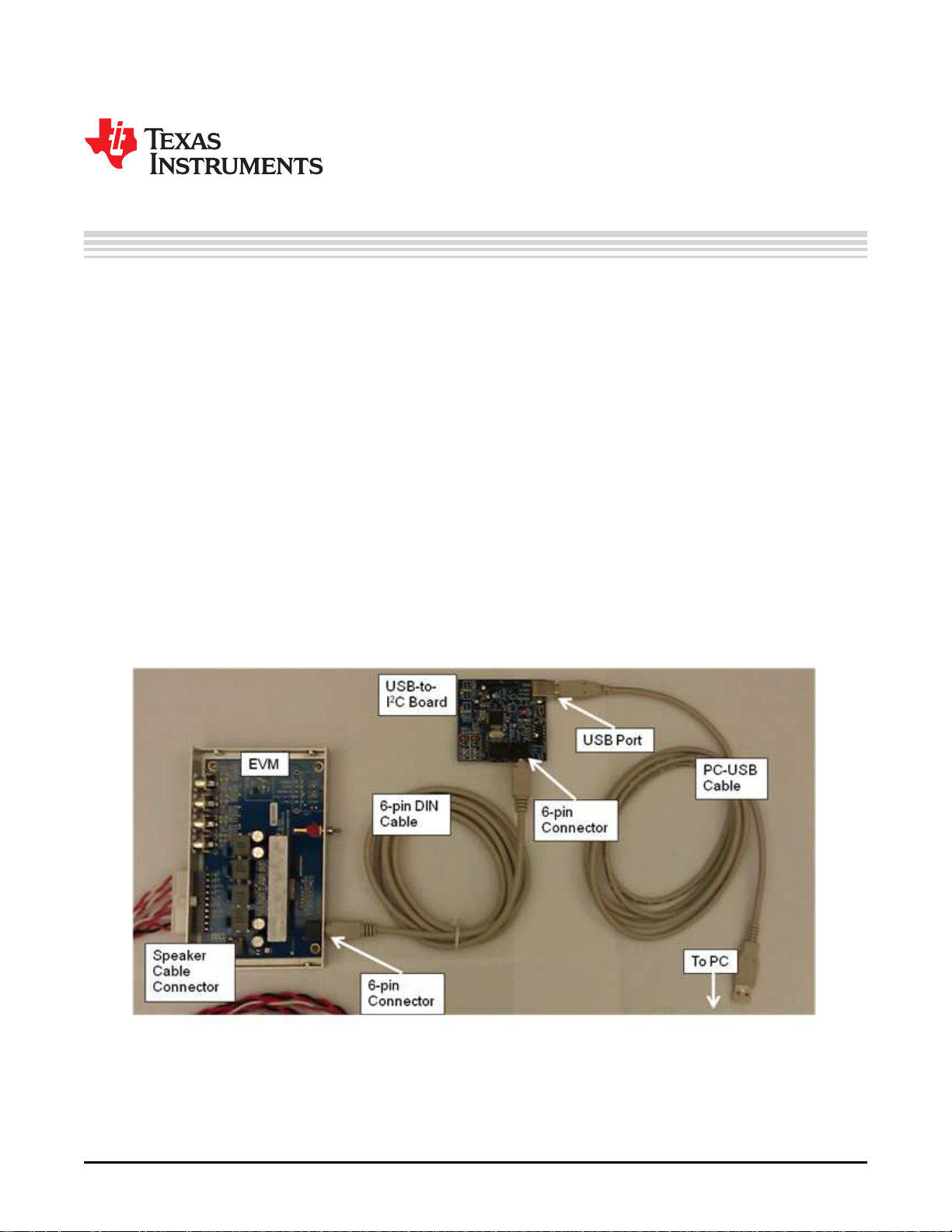
The EVM consists of a single printed circuit board (PCB) mounted inside a metal chassis for EMC testing.
The EVM must have an external I2C controller board to function. The USB-to-I2C controller board connects
to a personal computer (PC) through a USB cable. The EVM connects to the I2C controller through a
supplied 6-pin DIN cable. The PC needs the graphical user interface (GUI) software to control the EVM.
See Figure 1 for the device connections.
Software is available on the enclosed CDrom and provides the GUI, this document, and any other
necessary documents. Hardware provided in the EVM modules consists of the EVM, an I2C controller
board, a USB cable, a 6-pin DIN cable, and speaker cables.
User's Guide
SLOU359–January 2013
TAS5414C EVM User Guide
Figure 1. EVM to I2C Device Connections
1.2 Software Installation
The software is provided on the TI Web site. Run the setup.exe program to install the GUI. For more
details, see Section 1.5, Basic Graphical User Interface Controls.
SLOU359–January 2013 TAS5414C EVM User Guide
Submit Documentation Feedback
Copyright © 2013, Texas Instruments Incorporated
5
Page 6
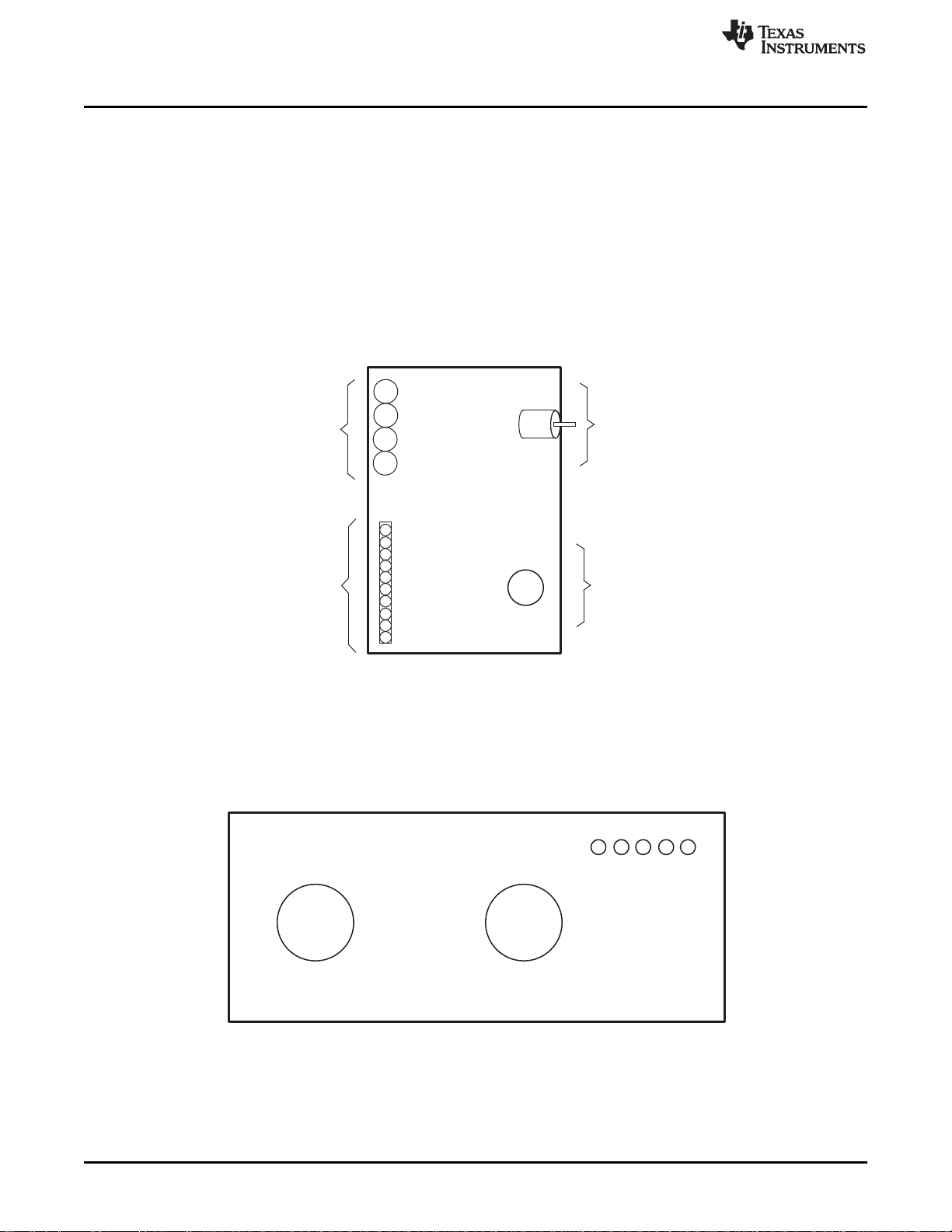
I C
2
Standby
OFF
Standby
ON
Fault
Clip OTW
Standby
Mute
Power
{
{
{
{
{
Standby Switch
6-pin DIN I C
Connector
2
Ch. 4
Ch. 3
Ch. 2
Ch. 1
PVDD
10-pin
connector for
speakers and
power
4 Audio RCA
Input
Connectors
Ch. 4
Ch. 3
Ch. 2
Ch. 1
Quick-Start Guide
1.3 Connections
The connections are for an analog signal for the input, speaker loads, power, and I2C. The audio inputs
are made through the four RCA connectors. The power connectors and speaker connectors are made
using the 10-pin connector.
The I2C connections are made through a 6-pin DIN connector. The provided adapter PCB and cable
connect the EVM to the PC. The adapter PCB is an I2C-to-USB converter, which is a human-interface
device (HID) and is automatically recognized by the PC when connected. Therefore, no drivers are
needed.
The basic connections are: PVDD or power is connected to the EVM through the supplied 10-pin
connector with the twisted red and black wires. The speakers or loads are also connected through the
same 10-pin connector with the twisted red and white wires. The 6-pin DIN is connected to the I2C-to-USB
adapter board. See Figure 2 for EVM input details.
www.ti.com
1.4 Initial Power Up
Before applying power, check to make sure the standby control switch is in the Standby OFF position, as
shown in Figure 3. If the switch is in the Standby ON position, then at power up the I2C LED indicator on
the GUI is red (see Section 3.4.3 for more details).
6
TAS5414C EVM User Guide SLOU359–January 2013
Figure 2. Connections for Input, Speaker Loads, Power, and I2C
Figure 3. End Panel for I2C Connections
Copyright © 2013, Texas Instruments Incorporated
Submit Documentation Feedback
Page 7
www.ti.com
Apply power: the Standby, Mute, and Power LEDs should be on. The Fault LED may also be on, but not
necessarily. This indicates that the unit is powered, and the TAS5414C or TAS5424C is in Standby Mode
and Mute Mode. The fault indicated is an undervoltage fault during power up. This is normal and is
cleared by reading I2C Register 0x00 (the Read Faults button) twice. Reading the faults once clears the
faults, and the second read is to ensure that all the faults have been cleared.
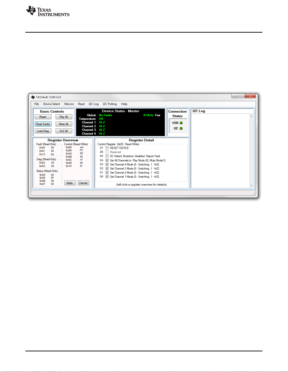
1.5 Basic Graphical User Interface Controls
The default state for the device is mute. To unmute, click the Play All button at the top left of the window.
To mute, click the Mute All button. The main EVM window is show in Figure 4.
EVM Description
2 EVM Description
2.1 Description of Inputs
2.1.1 Analog Inputs
The TAS5424C EVM provides balanced input and the TAS5414C EVM provides unbalanced (singleended) inputs. The four RCA jacks on either EVM are provided for the audio input. The unbalanced inputs
have the shield of the RCA connected to ground. The balanced inputs have the plus (+) input on the
center pin of the RCA and the minus (–) input on the shield. The balanced ground can be connected to
the chassis or Power– (GND).
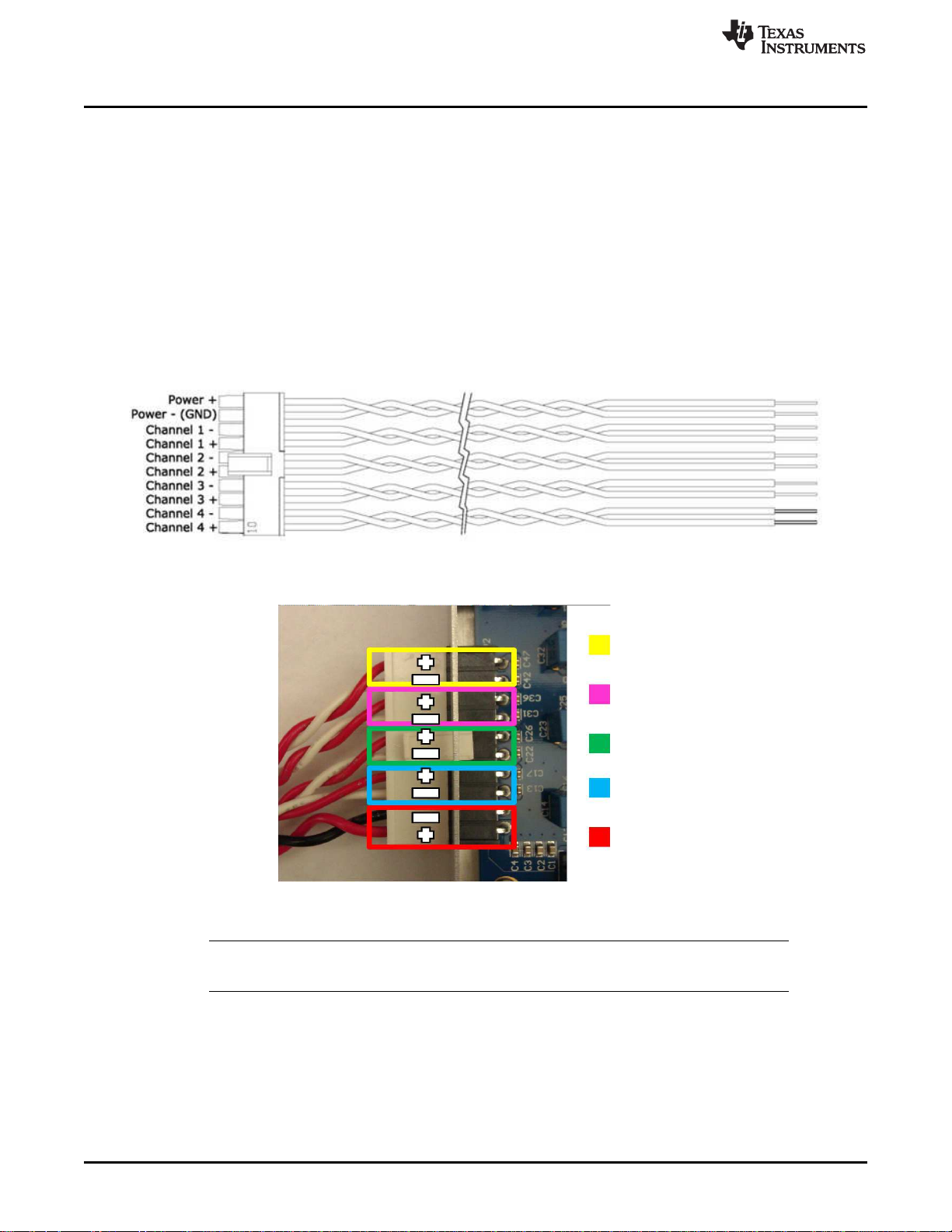
2.1.2 Power
The EVM requires one dc power connection. The connection is made through a 10-pin supplied
connector. The black wire is ground and the red wire is connected to PVDD, which can range from 6 to 24
Vdc.
Figure 4. Main Window
SLOU359–January 2013 TAS5414C EVM User Guide
Submit Documentation Feedback
Copyright © 2013, Texas Instruments Incorporated
7
Page 8
Ch. 4
Ch. 3
Ch. 2
Ch. 1
Power
EVM Description
2.2 Description of Outputs
2.2.1 Speaker and Power Connections
The 10-pin connector on the EVM and the wiring harness provide the power connections and the speaker
connections. The power connection consists of a pair of red and black twisted wires, which correspond to
the plus (+) output and minus (–) output, respectively. This pair of wires must be attached to a power
supply.
The speaker connections consist of the remaining four pairs of red and white twisted wire. Each pair of red
and white wires corresponds with a channel. The red wire corresponds to the plus (+) output, and the
white wire corresponds to the minus (–) output. These wires must be terminated to a speaker load or
resistive load.
See Figure 2 for more details on the 10-pin connector on the EVM, Figure 5 for more details about the
speaker cables, and Figure 6 for the speaker cables connection to the EVM.
www.ti.com
Figure 5. Wiring Harness for Power and Speaker Connections
Figure 6. Power and Speaker Connections to the EVM
NOTE: Do not connect any of the speaker outputs to ground. The TAS5414C and TAS5424C have
full bridged outputs; connecting to ground triggers a fault.
The outputs can be paralleled by connecting the plus (+) of one channel to the plus (+) of the other
channel. The minus (–) connection of one channel and the minus (–) connection of the other channel must
be connected also. See the data sheet for more details on parallel outputs (PBTL).
8
TAS5414C EVM User Guide SLOU359–January 2013
Copyright © 2013, Texas Instruments Incorporated
Submit Documentation Feedback
Page 9

www.ti.com
2.3 Controls
2.3.1 Standby
The standby switch is located next to the 6-pin DIN I2C input connector. Having the toggle in the Standby
ON position forces the TAS5414C or TAS5424C into the standby mode. This is the same as a power-on
reset (POR). POR shuts down the device, and I2C is not functional.
Setting the switch to the Standby OFF position puts the device in the EVM into its default power up mode.
The I2C registers are set to their defaults. The amplifier output is in Hi-Z mode.
2.4 Indicator Description
There are five LED indicators on the chassis next to the standby switch. The LED farthest away from the
standby switch is for the 3.3 Vdc supply. The 3.3 V supply is needed for the LEDs and the standby circuit.
The other four LEDs indicate the four non-I2C output pins: FAULT , CLIP_OTW, STANDBY, and MUTE.
The FAULT and CLIP_OTW signals are also routed to the 6-pin DIN for the GUI. In normal play mode,
these four LEDs should not light.
3 Graphical User Interface
3.1 Introduction
The TAS5414C/TAS5424C GUI software is designed to demonstrate the features of the TAS5414C and
TAS5424C. It is also able to assist the applications programmer in generating and saving the desired
operating characteristics.
The TAS5414C/TAS5424C GUI has a feature by which it can log the I2C data being sent to the device.
This can be helpful to the programmer in understanding the I2C commands needed for proper function.
Graphical User Interface
3.2 Software Installation
The GUI software is available on the CDrom provided with the EVM. Run the setup.exe program on a
personal computer (PC) with the Windows OS to install the GUI.
The software is currently supported up to Windows XP and is not supported by Windows 7.
The PC may need to connect to the internet to download the Microsoft .Net 2.0 environment, if it is not
already on the PC.
3.3 Hardware Installation
In the EVM package is a small PCB labeled USB2IIC2 on the PCB. This is the USB-to-I2C converter to
communicate from the PC to the EVM. Connect the USB cable to the PC and the PCB. Connect the 6-pin
cable to the connector labeled I2C on the converter PCB to the 6-pin connector on the EVM. The USB
connection provides power for this card. The PC should automatically connect to the USB-connected
PCB. See Figure 1, EVM to I2C Device Connections, for more details.
3.4 Using the GUI
3.4.1 The Main Window
3.4.1.1 TAS5414C Control Panel
The control panel consists of six buttons that perform basic functions on all four channels.
Reset: This button sends a software reset to the device via I2C. It is equivalent to sending 0x9F to register
0x0C. All the I2C defaults are restored.
Read Faults: This button reads the two fault registers 0x00 and 0x01 and reports the data to the Device
Status Panel.
SLOU359–January 2013 TAS5414C EVM User Guide
Submit Documentation Feedback
Copyright © 2013, Texas Instruments Incorporated
9
Page 10

Graphical User Interface
Load Diag: This button runs a script to perform the built-in load diagnostics and reports any faults to the
Device Status Panel. The details are displayed for each channel.
Play All: This button uses I2C to write 0x00 to register 0x0C which places all four channels into play
mode.
Mute All: This button uses I2C to set all channels to mute mode by writing 0x10 to register 0x0C. All
channels switch at 50% duty cycle, and no signal will pass from the input to the output.
Hi-Z All: This button places all four channel outputs into a high-impedance state by writing 0x1F to
register 0x0C. The device is first placed in mute. The Low-Low state is then invoked. Lastly, the outputs
are placed in Hi-Z.
3.4.2 Device Status Panel
Device Panel Title: The title at the top of the Device Status Panel shows which device the GUI is set to
communicate. The four options are: Master, Slave1, Slave 2, and Slave 3. This is changed in the menu
item Device Select.
Global: This provides fault feedback from the device. If a fault occurs a red Fault is indicated. Read the
fault detail in the register 0x00 and 0x01.
Temperature: This shows the temperature of the device. When the device is below 125°C, the color is
green. At Level 1 OTW, the color is yellow. At Level 2 OTW, the color is orange. At Level 3 OTW, the
color is red.
Channel 1-4: These four items provide individual channel output states: Hi-Z, Mute, Low-Low, and Play.
The gain setting will be displayed with the play indication.
Fsw: This item provides the switching frequency of the outputs.
www.ti.com
3.4.3 Connection Status Panel
There are two LED indicators to provide connection status.
USB: This indicator is gray when there is no USB connection to the USB2II2C PCB. The I2C LED is off.
The indicator is green when a connection is good.
I2C: This indicator is red when there is a USB connection, but no I2C connection. A green indicator shows
that I2C communication is functioning properly. If the LED is off, then there is no USB connection.
3.4.4 I2C Log Panel
All the I2C commands that are sent or received by the TAS5414C and TAS5424C are shown in this panel
except for I2C polling information. The displayed data can be copied to the clipboard for a programming
aid.
This type of information can be controlled by the I2C Log menu item. An R indicates a value read from the
device and a W indicates a value sent to the device. Valuable comments are also provided. Polling I2C
reads are not shown to prevent over-running the panel with background reads. See Section 3.4.7 for
further details on each tab.
3.4.5 Register Overview Panel
This panel provides the hexadecimal (hex) data for each I2C register. The hex data in the control registers
can be directly changed here and sent to the device with the Apply button. Any changes made to the data
are cleared by clicking the Cancel button. The Register Detail panel is changed either by changing the hex
value of the register directly or by clicking on the register and changing the specific bit in the Register
Detail panel. (See Section 3.4.6)
10
TAS5414C EVM User Guide SLOU359–January 2013
Copyright © 2013, Texas Instruments Incorporated
Submit Documentation Feedback
Page 11

www.ti.com
3.4.6 Register Detail Panel
This panel provides a detailed view of each register. By clicking on a register in the Register Overview
panel, the details of that register are shown. Each bit has its description and its value shown by the
checkbox. A checkbox with a check mark indicates a logical 1 and an unchecked checkbox indicates a
logical 0. Changes to each bit can be made by clicking on the checkbox. The changes are sent to the
device by clicking on the Apply button in the Register Overview panel.
3.4.7 Menu
File: In this menu, the Exit function can be found at the bottom of the drop-down menu.
Device Select: The I2C device select value can be changed in the Menu. For the EVM, use the default
value, which is Master.
Macros: In this menu, macros can be used. Macros are currently not being implemented at this time.
Custom Macros: This allows the users to create then save their own macros for later use.
Preloaded Macros: This menu item provides a list of built-in macros to perform typical I2C routines.
Read: The Read panel controls are located in this menu:
Fault Registers: When selected, the values of the fault registers are displayed in the I2C log. Note that
reading fault registers is different from reading faults. The data in a fault register is cleared on read.
The actual value displayed may show the fault, but the value in the device register will be cleared. A
second read of the fault registers will show a cleared fault register.
Load Diagnostic Registers: When selected, the values of the load diagnostic registers are read.
Status Registers: When selected, the values of the status registers are read.
Control Registers: When selected, the values of the control registers are read.
All Registers: When selected, the values of all the registers are read.
Options: The Options panel controls are located in this menu:
Crosstalk Compensation Enabled: When selected, Crosstalk is optimized. When this option is
disabled, the standard operation optimizes PSRR.
180 Phase Difference: When selected, the channels switch at 180° phase difference
Switching Frequency: When selected, the switching-frequency setting for AM avoidance can be
changed to 357 kHz or 500 kHz.
All Channels Gain: When selected, the gain on all the channels can be changed to 12 dB, 20 dB, or
32 dB.
I2C Log: The I2C Log panel controls are located in this menu:
Enabled: When selected, this menu option shows the I2C Log panel. When disabled, the I2C Log panel
is hidden.
Show I2C Reads: When selected, this menu option shows the values read from the device. These are
indicated with an R.
Show I2C Writes: When selected, this menu option shows the values that are sent to the device.
These are indicated with a W.
Show Comments: When selected, this menu option shows the comments. The comments are not
shown when this item is not selected.
Clear: This menu item clears the log data. The data is lost.
I2C Polling: The I2C Polling panel controls are located in this menu:
Enabled: When selected, the I2C actively samples the status registers specifically. When I2C Polling is
disabled, there is no guarantee that the register readings are valid.
Rate: When selected, the poll rate can be changed (in ms). The default setting is 250 ms.
Help: This menu item provides four items:
About: This provides the revision level of the software.
User Guide: This opens the User Guide in the AdobeTM AcrobatTM ReaderTM. Acrobat Reader
needs to be available on the PC.
Graphical User Interface
SLOU359–January 2013 TAS5414C EVM User Guide
Submit Documentation Feedback
Copyright © 2013, Texas Instruments Incorporated
11
Page 12

TAS5414/TAS5424C EVM Schematics
Device Webpage: This opens the TAS5414C/TAS5424C web page at the Texas Instruments Web site
in the default browser. The most-current data sheets, application reports, and GUI software is available
for downloading.
Check for EVM Updates: This checks to see if any new updates of the GUI are available.
4 TAS5414/TAS5424C EVM Schematics
The schematics for the TAS5414CPHD, TAS5414CDKD, and TAS5424CDKD are shown on the following
pages.
www.ti.com
12
TAS5414C EVM User Guide SLOU359–January 2013
Copyright © 2013, Texas Instruments Incorporated
Submit Documentation Feedback
Page 13

www.ti.com
TAS5414CPHD EVM Schematics
TAS5414/TAS5424C EVM Schematics
SLOU359–January 2013 TAS5414C EVM User Guide
Submit Documentation Feedback
Copyright © 2013, Texas Instruments Incorporated
13
Page 14

TAS5414/TAS5424C EVM Schematics
TAS5414CDKD EVM Schematics
www.ti.com
14
TAS5414C EVM User Guide SLOU359–January 2013
Copyright © 2013, Texas Instruments Incorporated
Submit Documentation Feedback
Page 15

www.ti.com
TAS5424CDKD EVM Schematics
TAS5414/TAS5424C EVM Schematics
SLOU359–January 2013 TAS5414C EVM User Guide
Submit Documentation Feedback
Copyright © 2013, Texas Instruments Incorporated
15
Page 16
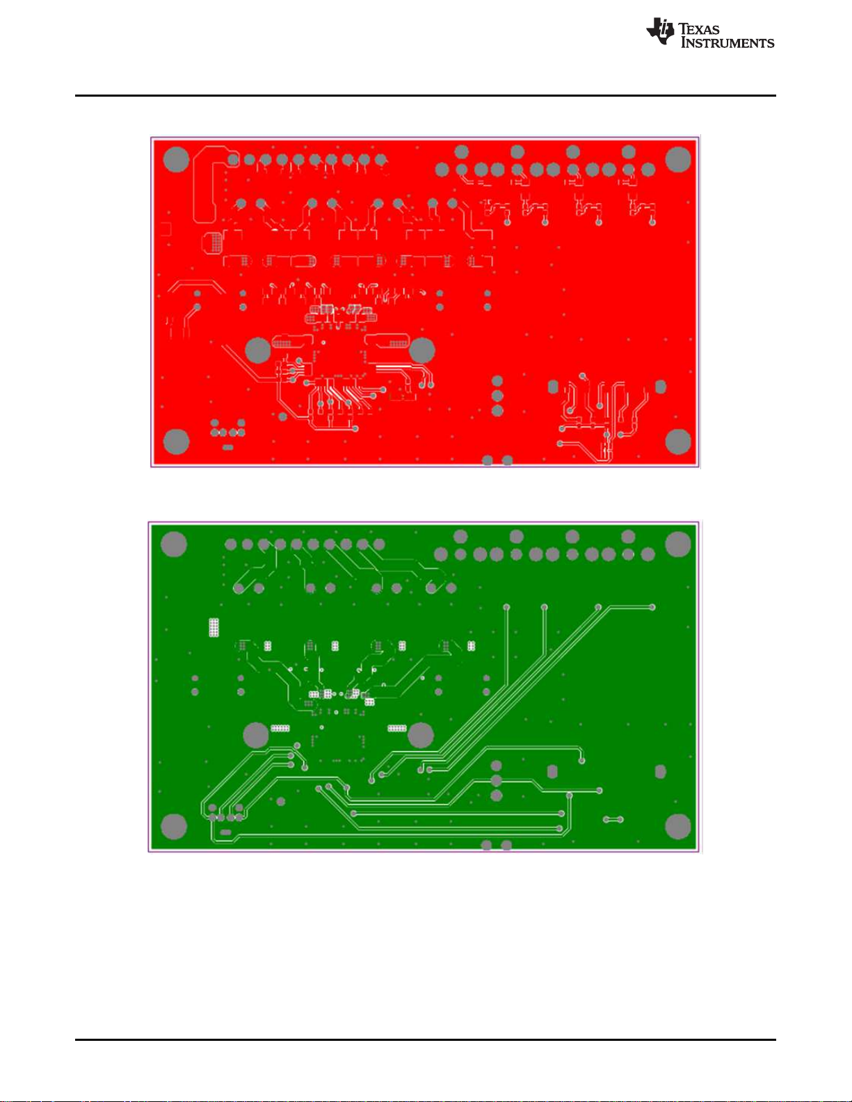
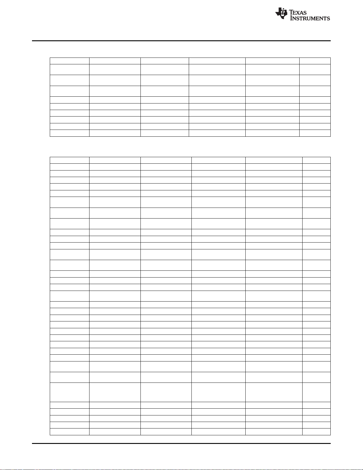
Board Layouts
5 Board Layouts
www.ti.com
Figure 7. TAS5414CPHD Top Layer
16
Figure 8. TAS5414CPHD Mid Layer Level 1
TAS5414C EVM User Guide SLOU359–January 2013
Copyright © 2013, Texas Instruments Incorporated
Submit Documentation Feedback
Page 17

www.ti.com
Board Layouts
Figure 9. TAS5414CPHD Mid Layer Level 2
Figure 10. TAS5414CPHD Bottom Layer
SLOU359–January 2013 TAS5414C EVM User Guide
Submit Documentation Feedback
Copyright © 2013, Texas Instruments Incorporated
17
Page 18

Board Layouts
www.ti.com
Figure 11. TAS5414CPHD Top Silkscreen Overlay
Figure 12. TAS5414CPHD Bottom Silkscreen Overlay
18
TAS5414C EVM User Guide SLOU359–January 2013
Copyright © 2013, Texas Instruments Incorporated
Submit Documentation Feedback
Page 19

www.ti.com
Board Layouts
Figure 13. TAS5414CDKD Top Layer
Figure 14. TAS5414CDKD Mid Layer Level 1
SLOU359–January 2013 TAS5414C EVM User Guide
Submit Documentation Feedback
Copyright © 2013, Texas Instruments Incorporated
19
Page 20

Board Layouts
www.ti.com
Figure 15. TAS5414CDKD Mid Layer Level 2
20
Figure 16. TAS5414CDKD Bottom Layer
TAS5414C EVM User Guide SLOU359–January 2013
Copyright © 2013, Texas Instruments Incorporated
Submit Documentation Feedback
Page 21

www.ti.com
Board Layouts
Figure 17. TAS5414CDKD Top Silkscreen Overlay
Figure 18. TAS5414CDKD Bottom Silkscreen Overlay
SLOU359–January 2013 TAS5414C EVM User Guide
Submit Documentation Feedback
Copyright © 2013, Texas Instruments Incorporated
21
Page 22

Board Layouts
www.ti.com
Figure 19. TAS5424CDKD Top Layer
22
Figure 20. TAS5424CDKD Mid Layer Level 1
TAS5414C EVM User Guide SLOU359–January 2013
Copyright © 2013, Texas Instruments Incorporated
Submit Documentation Feedback
Page 23

www.ti.com
Board Layouts
Figure 21. TAS5424CDKD Mid Layer Level 2
Figure 22. TAS5424CDKD Bottom Layer
SLOU359–January 2013 TAS5414C EVM User Guide
Submit Documentation Feedback
Copyright © 2013, Texas Instruments Incorporated
23
Page 24

Bill of Materials
www.ti.com
6 Bill of Materials
Table 1, Table 2, and Table 3 present the bill of materials for TAS5414CPHD, TAS5414CDKD, and
TAS5424CDKD respectively.
VALUE DESCRIPTION DESIGNATOR P/N P/N (DIGIKEY) QUANTITY
4.7 µF Capacitor, ceramic C1, C2 C2012X5R1E475K 445-4116-1-ND 2
0.082 µF Capacitor, ceramic C3 ECJ-2YB1H823K PCC1839CT 1
2200 pF Capacitor, ceramic C4 ECJ-2VB1H222K PCC222BNCT-ND 1
330 µF/35V Capacitor, electrolytic C5, C6,C7, C8 UVR1V331MPD 493-1083-ND 4
1 µF/50V Capacitor, ceramic C3216X7R1H105K 445-1423-1-ND 6
1 nF/50V Capacitor, ceramic ECJ-2VB1H102K PCC102BNCT-ND 8
150 nF/25V Capacitor, ceramic C2012X7R1E474K 445-1353-1-ND 8
10 nF/25V Capacitor, ceramic ECJ-1VB1E103K PCC1763CT-ND 8
470 nF/63V Capacitor, ceramic C14, C23, C32, C43 B32529C474J 495-1110-ND 4
220 nF Capacitor, ceramic C18 C0603C334K4RACTU 399-4916-1-ND 1
0.1 µF Capacitor, ceramic C19, C33, C57 ECJ-1VB1C104K PCC1762CT-ND 3
0.47 µF/16 V Capacitor, film C37, C39, C48, C52 ECP-U1C474MA5 PCF1130CT-ND 4
1200 pF/50 V Capacitor, ceramic C38, C44, C49, C54 ECJ-1VB1H122K PCC1773CT-ND 4
1 µF/16 V Capacitor, film C53, C55 ECP-U1C105MA5 PCF1132CT-ND 2
GRN Typical GREEN GaAs LED D1 SML-LX0603GW-TR 67-1549-1-ND 1
RED Typical RED GaAs LED D2, D3, D4 SML-LX0603SRW-TR 67-1551-1-ND 3
YEL Typical YELLOW GaAs LED D5 SML-LX0603YW-TR 67-1550-1-ND 1
Figure 23. TAS5424CDKD Top Silkscreen Overlay
Table 1. Bill of Materials for TAS5414CPHD
C9, C10,C27, C28,C50,
C51
C11, C15,C20, C24, C29,
C34, C40,C45
C12, C16,C21, C25, C30,
C35, C41,C46
C13, C17,C22, C26,C31,
C36, C42,C47
24
TAS5414C EVM User Guide SLOU359–January 2013
Submit Documentation Feedback
Copyright © 2013, Texas Instruments Incorporated
Page 25

www.ti.com
Channel 1, 2, 3, 4 RCA phono jack, right angle,
input thru-hole, snap-in
10 µH 10-µH inductor, SMT L1 Coilcraft SER1360H-103L 1
Dual_inductor Dual inductor L2, L3, L4, L5 Toko HEAW 4
LIGHTPIPE 5POS LP1 LPF-C051303S 1
Header 7 Header, 7-pin P1 MD-60S CP-2460 1
Output Header, 10-pin, right P2 SamtechIPBT-110-H1-T-S-RA 1
N MOS FET - P W/DIODE Q1 IRLMS5703TRPBF IRLMS5703PBFCT-ND 1
20 kΩ Resistor, SMT R1, R16 ERJ-3EKF2002V P20.0KHCT-ND 2
4.7 kΩ Resistor, SMT R2, R3 ERJ-3EKF4701V P4.70KHCT-ND 2
47 Ω Resistor, SMT R4 ERJ-3EKF47R0V P47.0HCT-ND 1
49.9 kΩ Resistor, SMT ERJ-3EKF4992V P49.9KHCT-ND 7
5.6 Ω Resistor, SMT RL1220S-5R6-F RL12S5.6FCT-ND 8
499 Ω Resistor, SMT ERJ-3EKF4990V P499HCT-ND 8
249 Ω Resistor, SMT R37 ERJ-3EKF2490V P249HCT-ND 1
470 Ω Resistor, SMT R44, R45, R46, R47 ERJ-3GEYJ471V P470GCT-ND 4
332 Ω Resistor, SMT R48 ERJ-3EKF3320V P332HCT-ND 1
S1 E-switch, SPDT, right-angle S1 100SP1T2B4M7RE EG2364-ND 1
TAS5414CPHD 4-channel class-D amplifier U1 TAS5414CTPHDRQ1 TAS5414CTPHDRQ1-ND 1
UA78M33CDCY Positive-voltage regulator U3 UA78M33CDCYR 296-13424-1-ND 1
Bill of Materials
Table 1. Bill of Materials for TAS5414CPHD (continued)
VALUE DESCRIPTION DESIGNATOR P/N P/N (DIGIKEY) QUANTITY
J1 RCJ-011 CP-1400-ND 4
R5, R6, R7, R23,R28, R33,
R36
R8, R10, R12, R14,R17,
R19, R26, R29
R21, R22, R24, R25,R31,
R32, R34, R35
Table 2. Bill of Materials for TAS5414CDKD
VALUE DESCRIPTION DESIGNATOR P/N P/N (DIGIKEY) QUANTITY
4.7 µF Capacitor, ceramic C1, C2 C2012X5R1E475K 445-4116-1-ND 2
0.082 µF Capacitor, ceramic C3 ECJ-2YB1H823K PCC1839CT 1
2200 pF Capacitor, ceramic C4 ECJ-2VB1H222K PCC222BNCT-ND 1
330 µF/35 V Capacitor, electrolytic C5, C6, C7, C8 UVR1V331MPD 493-1083-ND 4
1 µF/50 V Capacitor, ceramic C3216X7R1H105K 445-1423-1-ND 6
1 nF/50 V Capacitor, ceramic ECJ-2VB1H102K PCC102BNCT-ND 8
150 nF/25 V Capacitor, ceramic C2012X7R1E474K 445-1353-1-ND 8
10 nF/25 V Capacitor, ceramic ECJ-1VB1E103K PCC1763CT-ND 8
470 nF/63 V Capacitor, ceramic C14, C23, C32, C43 B32529C474J 495-1110-ND 4
220 nF Capacitor, ceramic C18 C0603C334K4RACTU 399-4916-1-ND 1
0.1 µF Capacitor, ceramic C19, C33, C57 ECJ-1VB1C104K PCC1762CT-ND 3
0.47 µF/16 V Capacitor, film C37, C39, C48, C52 ECP-U1C474MA5 PCF1130CT-ND 4
1200 pF/50 V Capacitor, ceramic C38, C44, C49, C54 ECJ-1VB1H122K PCC1773CT-ND 4
1 µF/16 V Capacitor, film C53, C55 ECP-U1C105MA5 PCF1132CT-ND 2
GRN Typical GREEN GaAs LED D1 SML-LX0603GW-TR 67-1549-1-ND 1
RED Typical RED GaAs LED D2, D3, D4 SML-LX0603SRW-TR 67-1551-1-ND 3
YEL Typical YELLOW GaAs LED D5 SML-LX0603YW-TR 67-1550-1-ND 1
Channel 1, 2, 3, 4 RCA phono jack, right angle,
input thru-hole, snap-in
10uH 10-µH Inductor, SMT L1 Coilcraft SER1360H-103L 1
Dual_inductor Dual inductor L2, L3, L4, L5 Toko HEAW 4
LIGHTPIPE 5POS LP1 LPF-C051303S 1
Header 7 Header, 7-pin P1 MD-60S CP-2460 1
Output Header, 10-pin, right P2 Samtech IPBT-110-H1-T-S-RA 1
N MOS FET - P W/DIODE Q1 IRLMS5703TRPBF IRLMS5703PBFCT-ND 1
20 kΩ Resistor, SMT R1, R16 ERJ-3EKF2002V P20.0KHCT-ND 2
4.7 kΩ Resistor, SMT R2, R3 ERJ-3EKF4701V P4.70KHCT-ND 2
47 Ω Resistor, SMT R4 ERJ-3EKF47R0V P47.0HCT-ND 1
C9, C10, C27, C28,C50,
C51
C11, C15, C20, C24, C29,
C34, C40, C45
C12, C16, C21, C25, C30,
C35, C41, C46
C13, C17, C22, C26,C31,
C36, C42, C47
J1 RCJ-011 CP-1400-ND 4
SLOU359–January 2013 TAS5414C EVM User Guide
Submit Documentation Feedback
Copyright © 2013, Texas Instruments Incorporated
25
Page 26
Bill of Materials
VALUE DESCRIPTION DESIGNATOR P/N P/N (DIGIKEY) QUANTITY
49.9 kΩ Resistor, SMT ERJ-3EKF4992V P49.9KHCT-ND 7
5.6 Ω Resistor, SMT RL1220S-5R6-F RL12S5.6FCT-ND 8
499 Ω Resistor, SMT ERJ-3EKF4990V P499HCT-ND 8
249 Ω Resistor, SMT R37 ERJ-3EKF2490V P249HCT-ND 1
470 Ω Resistor, SMT R44, R45, R46, R47 ERJ-3GEYJ471V P470GCT-ND 4
332 Ω Resistor, SMT R48 ERJ-3EKF3320V P332HCT-ND 1
S1 E-switch, SPDT, right-angle S1 100SP1T2B4M7RE EG2364-ND 1
TAS5414CDKD 4-channel class-D amplifier U1 TAS5414CTDKDRQ1 TAS5414CTDKDRQ1-ND 1
UA78M33CDCY Positive-voltage regulator U3 UA78M33CDCYR 296-13424-1-ND 1
VALUE DESCRIPTION DESIGNATOR P/N P/N (DIGIKEY) QUANTITY
4.7 µF Capacitor, ceramic C1, C2 C2012X5R1E475K 445-4116-1-ND 2
0.082 µF Capacitor, ceramic C3 ECJ-2YB1H823K PCC1839CT 1
2200 pF Capacitor, ceramic C4 ECJ-2VB1H222K PCC222BNCT-ND 1
330 µF/35 V Capacitor, electrolytic C5, C6, C7, C8 UVR1V331MPD 493-1083-ND 4
1 µF/50 V Capacitor, ceramic C9, C10, C27, C28,C50, C51 C3216X7R1H105K 445-1423-1-ND 6
1 nF/50 V Capacitor, ceramic ECJ-2VB1H102K PCC102BNCT-ND 8
150 nF/25 V Capacitor, ceramic C2012X7R1E474K 445-1353-1-ND 8
10 nF/25 V Capacitor, ceramic ECJ-1VB1E103K PCC1763CT-ND 8
470 nF/63 V Capacitor, ceramic C14, C23, C32, C43 B32529C474J 495-1110-ND 4
22 nF Capacitor, ceramic C18 C0603C334K4RACTU 399-4916-1-ND 1
0.1 µF Capacitor, ceramic C19, C33, C57 ECJ-1VB1C104K PCC1762CT-ND 3
0.47uF/16V Capacitor, film ECP-U1C474MA5 PCF1130CT-ND 8
1200 pF/50 V Capacitor, ceramic ECJ-1VB1H122K PCC1773CT-ND 8
GRN Typical GREEN GaAs LED D1 SML-LX0603GW-TR 67-1549-1-ND 1
RED Typical RED GaAs LED D2, D3, D4 SML-LX0603SRW-TR 67-1551-1-ND 3
YEL Typical YELLOW GaAs LED D5 SML-LX0603YW-TR 67-1550-1-ND 1
Channel 1, 2, 3, 4 RCA phono jack, right angle,
input thru-hole, snap-in
10 µH 10-µH inductor, SMT L1 Coilcraft SER1360H-103L 1
Dual_inductor Dual inductor L2, L3, L4, L5 Toko HEAW 4
LIGHTPIPE 5POS LP1 LPF-C051303S 1
Header 7 Header, 7-pin P1 MD-60S CP-2460 1
Output Header, 10-pin, right P2 Samtech IPBT-110-H1-T-S-RA 1
N MOS FET - P W/DIODE Q1 IRLMS5703TRPBF IRLMS5703PBFCT-ND 1
20 kΩ Resistor, SMT R1, R16 ERJ-3EKF2002V P20.0KHCT-ND 2
4.7 kΩ Resistor, SMT R2, R3 ERJ-3EKF4701V P4.70KHCT-ND 2
47 Ω Resistor, SMT R4 ERJ-3EKF47R0V P47.0HCT-ND 1
49.9 kΩ Resistor, SMT ERJ-3EKF4992V P49.9KHCT-ND 11
5.6 Ω Resistor, SMT RL1220S-5R6-F RL12S5.6FCT-ND 8
499 Ω Resistor, SMT ERJ-3EKF4990V P499HCT-ND 16
470 Ω Resistor, SMT R44, R45, R46, R47 ERJ-3GEYJ471V P470GCT-ND 4
332 Ω Resistor, SMT R48 ERJ-3EKF3320V P332HCT-ND 1
S1 E-switch, SPDT, right-angle S1 100SP1T2B4M7RE EG2364-ND 1
TAS5424CDKD 4-channel class-D amplifeir U2 TAS5424CTDKDRQ1 TAS5424CTDKDRQ1-ND 1
UA78M33CDCY Positive-voltage regulator U3 UA78M33CDCYR 296-13424-1-ND 1
Table 2. Bill of Materials for TAS5414CDKD (continued)
R5, R6, R7, R23,R28, R33,
R36
R8, R10, R12, R14,R17,
R19, R26, R29
R21, R22, R24, R25,R31,
R32, R34, R35
Table 3. Bill of Materials for TAS5424CDKD
C11, C15, C20, C24, C29,
C34, C40, C45
C12, C16, C21, C25, C30,
C35, C41, C46
C13, C17, C22, C26,C31,
C36, C42, C47
C37, C44, C48, C53, C54,
C59, C60, C63
C38, C39, C49, C52, C55,
C58, C61, C62
J1 RCJ-011 CP-1400-ND 4
R5, R6, R7, R23, R9, R20,
R24, R31, R32, R37, R49
R8, R10, R12, R14,R17, R19,
R26, R29
R21, R22, R11, R13, R15,
R18, R25, R27, R28, R30,
R33, R34, R35, R36, R50,
R51
www.ti.com
26
TAS5414C EVM User Guide SLOU359–January 2013
Submit Documentation Feedback
Copyright © 2013, Texas Instruments Incorporated
Page 27

www.ti.com
7 Related Documentation from Texas Instruments
The TAS5414C, TAS5424C, Four-Channel Automotive Digital Amplifiers data sheet can be found online at
www.ti.com.
Related Documentation from Texas Instruments
SLOU359–January 2013 TAS5414C EVM User Guide
Submit Documentation Feedback
Copyright © 2013, Texas Instruments Incorporated
27
Page 28

Evaluation Board/Kit Important Notice
Texas Instruments (TI) provides the enclosed product(s) under the following conditions:
This evaluation board/kit is intended for use for ENGINEERING DEVELOPMENT, DEMONSTRATION, OR EVALUATION PURPOSES
ONLY and is not considered by TI to be a finished end-product fit for general consumer use. Persons handling the product(s) must have
electronics training and observe good engineering practice standards. As such, the goods being provided are not intended to be complete
in terms of required design-, marketing-, and/or manufacturing-related protective considerations, including product safety and environmental
measures typically found in end products that incorporate such semiconductor components or circuit boards. This evaluation board/kit does
not fall within the scope of the European Union directives regarding electromagnetic compatibility, restricted substances (RoHS), recycling
(WEEE), FCC, CE or UL, and therefore may not meet the technical requirements of these directives or other related directives.
Should this evaluation board/kit not meet the specifications indicated in the User’s Guide, the board/kit may be returned within 30 days from
the date of delivery for a full refund. THE FOREGOING WARRANTY IS THE EXCLUSIVE WARRANTY MADE BY SELLER TO BUYER
AND IS IN LIEU OF ALL OTHER WARRANTIES, EXPRESSED, IMPLIED, OR STATUTORY, INCLUDING ANY WARRANTY OF
MERCHANTABILITY OR FITNESS FOR ANY PARTICULAR PURPOSE.
The user assumes all responsibility and liability for proper and safe handling of the goods. Further, the user indemnifies TI from all claims
arising from the handling or use of the goods. Due to the open construction of the product, it is the user’s responsibility to take any and all
appropriate precautions with regard to electrostatic discharge.
EXCEPT TO THE EXTENT OF THE INDEMNITY SET FORTH ABOVE, NEITHER PARTY SHALL BE LIABLE TO THE OTHER FOR ANY
INDIRECT, SPECIAL, INCIDENTAL, OR CONSEQUENTIAL DAMAGES.
TI currently deals with a variety of customers for products, and therefore our arrangement with the user is not exclusive.
TI assumes no liability for applications assistance, customer product design, software performance, or infringement of patents or
services described herein.
Please read the User’s Guide and, specifically, the Warnings and Restrictions notice in the User’s Guide prior to handling the product. This
notice contains important safety information about temperatures and voltages. For additional information on TI’s environmental and/or
safety programs, please contact the TI application engineer or visit www.ti.com/esh.
No license is granted under any patent right or other intellectual property right of TI covering or relating to any machine, process, or
combination in which such TI products or services might be or are used.
FCC Warning
This evaluation board/kit is intended for use for ENGINEERING DEVELOPMENT, DEMONSTRATION, OR EVALUATION PURPOSES
ONLY and is not considered by TI to be a finished end-product fit for general consumer use. It generates, uses, and can radiate radio
frequency energy and has not been tested for compliance with the limits of computing devices pursuant to part 15 of FCC rules, which are
designed to provide reasonable protection against radio frequency interference. Operation of this equipment in other environments may
cause interference with radio communications, in which case the user at his own expense will be required to take whatever measures may
be required to correct this interference.
EVM Warnings and Restrictions
It is important to operate this EVM within the input voltage range of 6 V to 24 V and the output voltage range of 6 V to 24 V.
Exceeding the specified input range may cause unexpected operation and/or irreversible damage to the EVM. If there are questions
concerning the input range, please contact a TI field representative prior to connecting the input power.
Applying loads outside of the specified output range may result in unintended operation and/or possible permanent damage to the EVM.
Please consult the EVM User's Guide prior to connecting any load to the EVM output. If there is uncertainty as to the load specification,
please contact a TI field representative.
During normal operation, some circuit components may have case temperatures greater than 115°C. The EVM is designed to operate
properly with certain components above 115°C as long as the input and output ranges are maintained. These components include but are
not limited to linear regulators, switching transistors, pass transistors, and current sense resistors. These types of devices can be identified
using the EVM schematic located in the EVM User's Guide. When placing measurement probes near these devices during operation,
please be aware that these devices may be very warm to the touch.
Mailing Address: Texas Instruments, Post Office Box 655303, Dallas, Texas 75265
Copyright © 2013, Texas Instruments Incorporated
Page 29

IMPORTANT NOTICE
Texas Instruments Incorporated and its subsidiaries (TI) reserve the right to make corrections, enhancements, improvements and other
changes to its semiconductor products and services per JESD46, latest issue, and to discontinue any product or service per JESD48, latest
issue. Buyers should obtain the latest relevant information before placing orders and should verify that such information is current and
complete. All semiconductor products (also referred to herein as “components”) are sold subject to TI’s terms and conditions of sale
supplied at the time of order acknowledgment.
TI warrants performance of its components to the specifications applicable at the time of sale, in accordance with the warranty in TI’s terms
and conditions of sale of semiconductor products. Testing and other quality control techniques are used to the extent TI deems necessary
to support this warranty. Except where mandated by applicable law, testing of all parameters of each component is not necessarily
performed.
TI assumes no liability for applications assistance or the design of Buyers’ products. Buyers are responsible for their products and
applications using TI components. To minimize the risks associated with Buyers’ products and applications, Buyers should provide
adequate design and operating safeguards.
TI does not warrant or represent that any license, either express or implied, is granted under any patent right, copyright, mask work right, or
other intellectual property right relating to any combination, machine, or process in which TI components or services are used. Information
published by TI regarding third-party products or services does not constitute a license to use such products or services or a warranty or
endorsement thereof. Use of such information may require a license from a third party under the patents or other intellectual property of the
third party, or a license from TI under the patents or other intellectual property of TI.
Reproduction of significant portions of TI information in TI data books or data sheets is permissible only if reproduction is without alteration
and is accompanied by all associated warranties, conditions, limitations, and notices. TI is not responsible or liable for such altered
documentation. Information of third parties may be subject to additional restrictions.
Resale of TI components or services with statements different from or beyond the parameters stated by TI for that component or service
voids all express and any implied warranties for the associated TI component or service and is an unfair and deceptive business practice.
TI is not responsible or liable for any such statements.
Buyer acknowledges and agrees that it is solely responsible for compliance with all legal, regulatory and safety-related requirements
concerning its products, and any use of TI components in its applications, notwithstanding any applications-related information or support
that may be provided by TI. Buyer represents and agrees that it has all the necessary expertise to create and implement safeguards which
anticipate dangerous consequences of failures, monitor failures and their consequences, lessen the likelihood of failures that might cause
harm and take appropriate remedial actions. Buyer will fully indemnify TI and its representatives against any damages arising out of the use
of any TI components in safety-critical applications.
In some cases, TI components may be promoted specifically to facilitate safety-related applications. With such components, TI’s goal is to
help enable customers to design and create their own end-product solutions that meet applicable functional safety standards and
requirements. Nonetheless, such components are subject to these terms.
No TI components are authorized for use in FDA Class III (or similar life-critical medical equipment) unless authorized officers of the parties
have executed a special agreement specifically governing such use.
Only those TI components which TI has specifically designated as military grade or “enhanced plastic” are designed and intended for use in
military/aerospace applications or environments. Buyer acknowledges and agrees that any military or aerospace use of TI components
which have not been so designated is solely at the Buyer's risk, and that Buyer is solely responsible for compliance with all legal and
regulatory requirements in connection with such use.
TI has specifically designated certain components as meeting ISO/TS16949 requirements, mainly for automotive use. In any case of use of
non-designated products, TI will not be responsible for any failure to meet ISO/TS16949.
Products Applications
Audio www.ti.com/audio Automotive and Transportation www.ti.com/automotive
Amplifiers amplifier.ti.com Communications and Telecom www.ti.com/communications
Data Converters dataconverter.ti.com Computers and Peripherals www.ti.com/computers
DLP® Products www.dlp.com Consumer Electronics www.ti.com/consumer-apps
DSP dsp.ti.com Energy and Lighting www.ti.com/energy
Clocks and Timers www.ti.com/clocks Industrial www.ti.com/industrial
Interface interface.ti.com Medical www.ti.com/medical
Logic logic.ti.com Security www.ti.com/security
Power Mgmt power.ti.com Space, Avionics and Defense www.ti.com/space-avionics-defense
Microcontrollers microcontroller.ti.com Video and Imaging www.ti.com/video
RFID www.ti-rfid.com
OMAP Applications Processors www.ti.com/omap TI E2E Community e2e.ti.com
Wireless Connectivity www.ti.com/wirelessconnectivity
Mailing Address: Texas Instruments, Post Office Box 655303, Dallas, Texas 75265
Copyright © 2013, Texas Instruments Incorporated
 Loading...