

TM
www.ti.com
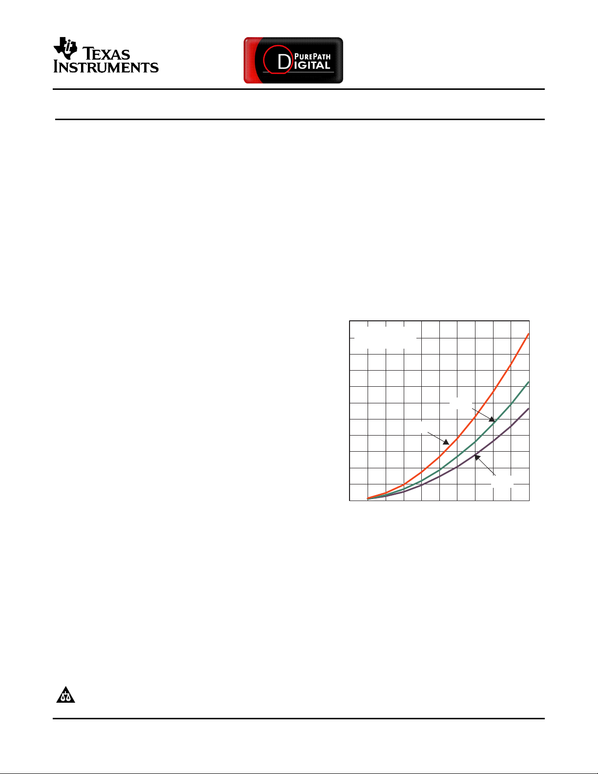
PVDD Supply Voltage − V
0
30
60
90
120
150
180
210
240
270
300
330
0 5 10 15 20 25 30 35 40 45 50
TC = 75°C
THD+N at 10%
P
O
− Output Power − W
G001
8 Ω
6 Ω
4 Ω
315-W Mono BTL Digital Amplifier Power Stage
FEATURES
• Total Output Power
– 125 W Into 8 Ω at <0.09% THD+N
– 220 W Into 6 Ω at 10% THD+N
– 315 W Into 4 Ω at 10% THD+N
• 110-dB SNR (A-Weighted with TAS5518
modulator)
• Supports Pulse-Width Modulation (PWM)
Frame Rates of 192 kHz to 384 kHz
• Resistor-Programmable Current Limit
• Integrated Self-Protection Circuit Including:
– Under Voltage Protection
– Over Temperature Warning and Error
– Over Load Protection
– Short Circuit (OC) Protection
– PWM Activity Dectector
• Power-On Reset (POR) to Eliminate System
Power-Supply Sequencing
• Thermally-Enhanced Package DKD (36-pin
PSOP3)
• EMI Compliant When Used With
Recommended System Design
• Error Reporting 3.3-V and 5-V Compliant
TAS5261
SLES188 – AUGUST 2006
The TAS5261 has complete protection circuitry
integrated on chip, safeguarding the device and
speakers against fault conditions that could damage
the system. These protection features are
short-circuit protection, overcurrent protection,
undervoltage protection, and a loss of pulse-width
modulation (PWM) input signal (PWM Activity
Detector).
A power-on reset (POR) circuit is used to eliminate
power-supply sequencing that is normally required
for most H-bridge designs.
OUTPUT POWER
vs
PVDD_x SUPPLY VOLTAGE
APPLICATIONS
• AV Receivers
• DVD Receivers
• Mini/Micro Component Systems
• Home Theater Systems
DESCRIPTION
The TAS5261 is a high-performance, integrated
mono digital amplifier power stage designed to drive
4- Ω to 8- Ω speakers with low harmonic distortion.
This system requires only a simple, passive
demodulation filter to deliver high-quality,
high-efficiency audio amplification.
Please be aware that an important notice concerning availability, standard warranty, and use in critical applications of Texas
Instruments semiconductor products and disclaimers thereto appears at the end of this data sheet.
PowerPAD is a trademark of Texas Instruments.
PRODUCTION DATA information is current as of publication date.
Products conform to specifications per the terms of the Texas
Instruments standard warranty. Production processing does not
necessarily include testing of all parameters.
Copyright © 2006, Texas Instruments Incorporated
www.ti.com
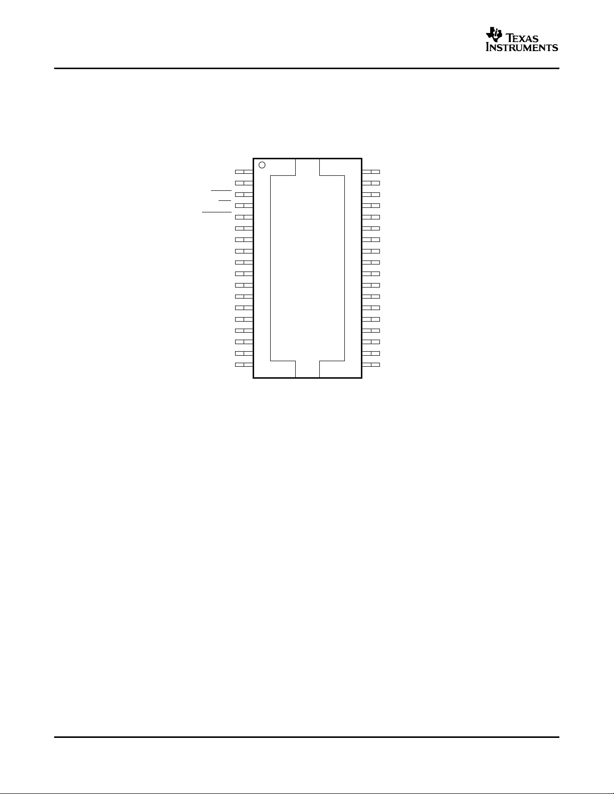
1
2
3
4
5
6
7
8
9
10
11
12
13
14
15
16
17
18
36
35
34
33
32
31
30
29
28
27
26
25
24
23
22
21
20
19
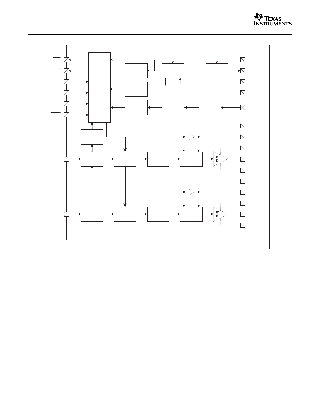
BST_A
GVDD_A
OTW
SD
RESET
PWM_A
OC_ADJ
GND
AGND
VREG
M3
M2
M1
PWM_B
VDD
GND
GVDD_B
BST_B
PVDD_A
PVDD_A
PVDD_A
PGND
PGND
PGND
OUT_A
OUT_A
OUT_A
OUT_B
OUT_B
OUT_B
PGND
PGND
PGND
PVDD_B
PVDD_B
PVDD_B
DKDPACKAGE
(TOP VIEW)
P0018-02
TAS5261
SLES188 – AUGUST 2006
DEVICE INFORMATION
The TAS5261 is available in a thermally-enhanced 36-pin PSOP3 PowerPAD™ package. The heat slug is
located on the top side of the device for convenient thermal coupling to a heat sink.
2
Submit Documentation Feedback
www.ti.com
DISSIPATION RATINGS
PARAMETER CONDITION TYPICAL (DKD)
R
θ JC
R
θ JC
BTL channel (four transistors) 0.6 ° C/W
One transistor 2.38 ° C/W
Pad area 80 mm
Protection Mode
Protection modes are selected by shorting M1, M2, and M3 to VREG or GND.
Table 1. Protection Modes
MODE PINS
(1)
M3
M2 M1
0 0 0 Full protection (default)
0 0 1 Reserved
0 1 0 OC latching mode
0 1 1 Reserved
(1) M3 is reserved and always should be connected to board GND.
PROTECTION MODE
TAS5261
SLES188 – AUGUST 2006
2
Submit Documentation Feedback
3

www.ti.com
TAS5261
SLES188 – AUGUST 2006
TERMINAL FUNCTIONS
TERMINAL
NAME PIN NO.
AGND 9 I Analog ground
BST_A 1 P Bootstrap, A side
BST_B 18 I Bootstrap, B side
GND 8, 16 I Power ground
GVDD_A 2 P Gate-drive voltage supply, A side
GVDD_B 17 I Gate-drive voltage supply, B side
M1 13 I Mode-selection 1 (LSB)
M2 12 I Mode-selection 2 (MSB)
M3 11 I Reserved
OC_ADJ 7 I Overcurrent threshold programming
OTW 3 O Overtemperature warning. Open drain, active low.
OUT_A 28, 29, 30 O Output, half-bridge A
OUT_B 25, 26, 27 O Output, half-bridge B
PGND P Power ground
PWM_A 6 I PWM for half-bridge A
PWM_B 14 I PWM Input for half-bridge B
PVDD_A 34, 35, 36 P PVDD supply for half-bridge A
PVDD_B 19, 20, 21 P PVDD supply for half-bridge B
RESET 5 I Reset. Active low.
SD 4 O Shutdown. Open drain, active low.
VDD 15 I Input power supply
VREG 10 O Internal voltage regulator
22, 23, 24, 31,
32, 33
I/O DESCRIPTION
4
Submit Documentation Feedback
www.ti.com
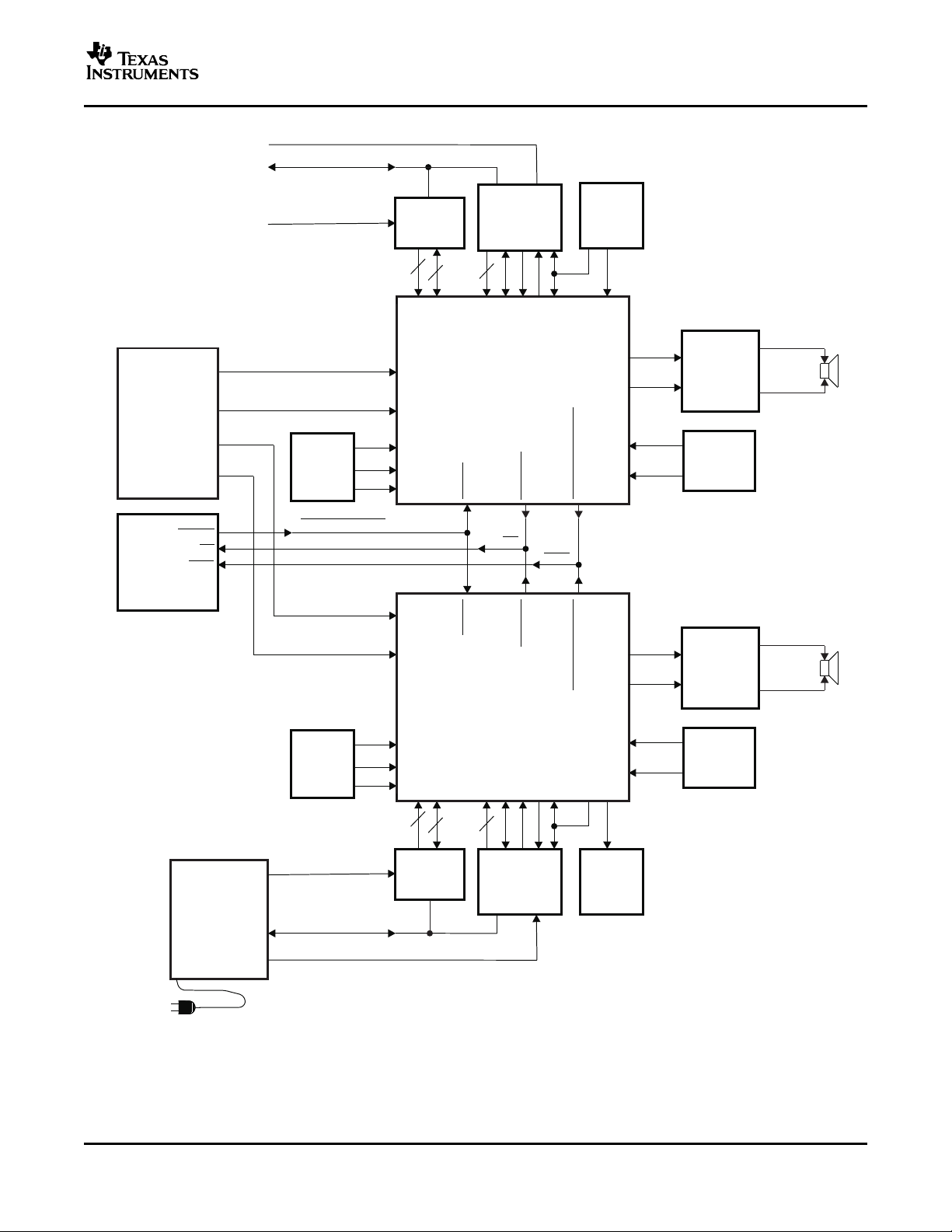
B0101-01
PVDD(0–50V)
Mono
BTL
H-Bridge
Hardwire
Mode
Control
Hardwire
Mode
Control
M1
M1
M2
M2
M3
M3
System
Microcontroller
RESET_H-Bridge
SD
OTW
OTW
SD
RESET
Hardwire
Over-
current
Limit
Hardwire
Over-
current
Limit
PVDD
Power-Supply
Decoupling
PVDD
Power-Supply
Decoupling
GVDD,VDD,
andVREG
Power-Supply
Decoupling
GVDD,VDD,
andVREG
Power-Supply
Decoupling
6
6
6
6
2
2
GVDD(12V)andVDD(12V)
GVDD(12V)andVDD(12V)
GND
GND
PVDD(0–50V)
System
Power
Supplies
50V
12V
GND
AC
Bootstrap
Capacitors
Bootstrap
Capacitors
BST_A
BST_A
BST_B
BST_B
R2
L2
PWM_B
RESET
Shutdown
Overtemp_warning
R1
L1
TAS55XX
Left
Output
Right
Output
PWM_A
H-Bridge
Output
H-Bridge
Output
PVDD_A,B
VDD
VREG
GND
GND
GVDD_A,B
GND_A,B
OC_ADJ
Mono
BTL
H-Bridge
PWM_B
RESET
Shutdown
Overtemp_warning
PWM_A
PVDD_A,B
VDD
VREG
GND
GND
GVDD_A,B
GND_A,B
OC_ADJ
2nd-Order
L-COutput
Filterfor
Each
H-Bridge
2nd-Order
L-COutput
Filterfor
Each
H-Bridge
OUT_A
OUT_A
OUT_B
OUT_B
4–8
(3 Min)
W
W
4–8
(3 Min)
W
W
TAS5261
SLES188 – AUGUST 2006
Figure 1. Typical System Block Diagram
Submit Documentation Feedback
5
www.ti.com
TEMP
SENSE
M1
M2
AGND
OC_
ADJ
VREG VREG
VDD
GVDD
_B
M3
P
OWER-UP
R
ESET
U
VP
GND
PWM
_B
OUT_B
(x3)
PGND
(x3)
PVDD_B
(x3)
BST_B
TIMING
CONTROL
GATE-DRIVECONTROL
PWM
RECEIVER
OVER-LOAD
PROT
.
GVDD
_A
PWM
ACTIVITY
DETECTOR
CB
3C
GVDD
_B
CURRENT
SENSE
GVDD
_A
PWM
_A
OUT_A(
x3)
PGND
(x3)
PVDD_A(
x3)
BST_A
TIMING
CONTROL
CONTROL GATE-DRIVE
PWM
RECEIVER
PROTECTION & I/O LOGIC
OTW
SD
RESET
TAS5261
SLES188 – AUGUST 2006
Figure 2. Functional Block Diagram
6
Submit Documentation Feedback
www.ti.com
ORDERING INFORMATION
T
A
0 ° C to 70 ° C TAS5261DKD 36-pin PSOP3
PACKAGE DESCRIPTION
TAS5261
SLES188 – AUGUST 2006
Absolute Maximum Ratings
(1)
over operating free-air temperature range (unless otherwise noted)
MIN MAX UNIT
VDD to AGND –0.3 13.2 V
GVDD_x to AGND –0.3 13.2 V
PVDD_x to PGND_x
OUT_x to PGND_x
BST_x to PGND_x
BST_x to GVDD_x
VREG to AGND –0.3 4.2 V
PGND_x to GND –0.3 0.3 V
PGND_x to AGND –0.3 0.3 V
GND to AGND –0.3 0.3 V
PWM_x, OC_ADJ, M1, M2, M3 to AGND –0.3 4.2 V
RESET, SD, OTW to AGND –0.3 7 V
Maximum continuous sink current ( SD, OTW) 9 mA
Maximum operating junction temperature range, T
Storage temperature range, T
Lead temperature 1,6 mm (1/16 in) from case for 10 s 260 ° C
Minimum pulse duration, low – minimum pulse width must be ensured by the PWM processor 50 ns
(1) Stresses beyond those listed under "absolute maximum ratings" may cause permanent damage to the device. These are only stress
ratings, and functional operation of the device at these or any other conditions beyond those indicated under "recommended operating
conditions" is not implied. Exposure to absolute-maximum-rated conditions for extended periods may affect device reliability.
(2) These voltages represent the dc voltage + peak ac waveform measured at the terminal of the device in all conditions.
(2)
(2)
(2)
(2)
J
stg
–0.3 71 V
–0.3 71 V
–0.3 79.7 V
–0.3 66.5 V
0 150 ° C
–65 150 ° C
Submit Documentation Feedback
7
 Loading...