

Texas Instruments TAS5162, TAS5162DKDRG4 Datasheet

TM
www.ti.com
0
220
20
40
60
80
100
120
140
160
180
200
0505 10
15
20
25 30
35
40 45
PV -SupplyVoltage(BTL)-Vrms
DD
P -OutputPower-W
O
4 W
6 W
T =75°C
C
8 W
2 x 210 Watt STEREO DIGITAL AMPLIFIER POWER STAGE
TAS5162
SLES194C – OCTOBER 2006 – REVISED MAY 2007
FEATURES
• 2 × 160 W at 10% THD+N Into 8- Ω BTL
• 2 × 210 W at 10% THD+N Into 6- Ω BTL
• 1 × 300 W at 10% THD+N Into 4- Ω PBTL
• >110 dB SNR (A-Weighted, TAS5518
Modulator)
• <0.09% THD+N at 1 W
• Two Thermally Enhanced Package Options:
– DKD (36-pin PSOP3)
– DDV (44-pin HTSSOP)
• High-Efficiency Power Stage (>90%) With
80-m Ω Output MOSFETs
• Power-On Reset for Protection on Power Up
Without Any Power-Supply Sequencing
• Integrated Self-Protection Circuits Including
Undervoltage, Overtemperature, Overload,
Short Circuit
• Error Reporting
• EMI Compliant When Used With
Recommended System Design
• Intelligent Gate Drive
• Mid-Z Ramp Compatible for reduced "pop
noise"
This system only requires a simple passive LC
demodulation filter to deliver high-quality,
high-efficiency audio amplification with proven EMI
(1)
compliance. This device requires two power
supplies, at 12 V for GVDD and VDD, and at 50V for
PVDD. The TAS5162 does not require power-up
sequencing due to internal power-on reset. The
efficiency of this digital amplifier is greater than 90%
into 6 Ω , which enables the use of smaller power
supplies and heatsinks.
The TAS5162 has an innovative protection system
integrated on-chip, safeguarding the device against a
wide range of fault conditions that could damage the
system. These safeguards are short-circuit
protection, overcurrent protection, undervoltage
protection, and overtemperature protection. The
TAS5162 has a new proprietary current-limiting
circuit that reduces the possibility of device shutdown
during high-level music transients. A new
programmable overcurrent detector allows the use of
lower-cost inductors in the demodulation output filter.
BTL OUTPUT POWER vs SUPPLY VOLTAGE
APPLICATIONS
• Mini/Micro Audio System
• DVD Receiver
• Home Theater
DESCRIPTION
The TAS5162 is a high performance, integrated
stereo digital amplifier power stage with an improved
protection system. The TAS5162 is capable of
driving a 6- Ω bridge-tied load (BTL) at up to 210 W
per channel at THD = 10%, low integrated noise at
the output, low THD+N performance without clipping,
and low idle power dissipation.
A low-cost, high-fidelity audio system can be built
using a TI chipset, comprising a modulator (e.g.,
TAS5508) and the TAS5162. PurePath Digital™
PurePath Digital, PowerPad are trademarks of Texas Instruments.
All other trademarks are the property of their respective owners.
PRODUCTION DATA information is current as of publication date.
Products conform to specifications per the terms of the Texas
Instruments standard warranty. Production processing does not
necessarily include testing of all parameters.
(1) The DDV package will deliver the stated maximum power
levels; however, this is dependant on system
Please be aware that an important notice concerning availability, standard warranty, and use in critical applications of Texas
Instruments semiconductor products and disclaimers thereto appears at the end of this data sheet.
configuration. The smaller pad area also makes the
thermal interface to the heatsink more important. For
multichannel systems that require two channels to be
driven at full power with the DDV package option, it is
recommended to design the system so that the two
channels are in two separate devices.
Copyright © 2006–2007, Texas Instruments Incorporated
www.ti.com
1
2
3
4
5
6
7
8
9
10
11
12
13
14
15
16
17
18
36
35
34
33
32
31
30
29
28
27
26
25
24
23
22
21
20
19
GVDD_B
OTW
SD
PWM_A
RESET_AB
PWM_B
OC_ADJ
GND
AGND
VREG
M3
M2
M1
PWM_C
RESET_CD
PWM_D
VDD
GVDD_C
GVDD_A
BST_A
PVDD_A
OUT_A
GND_A
GND_B
OUT_B
PVDD_B
BST_B
BST_C
PVDD_C
OUT_C
GND_C
GND_D
OUT_D
PVDD_D
BST_D
GVDD_D
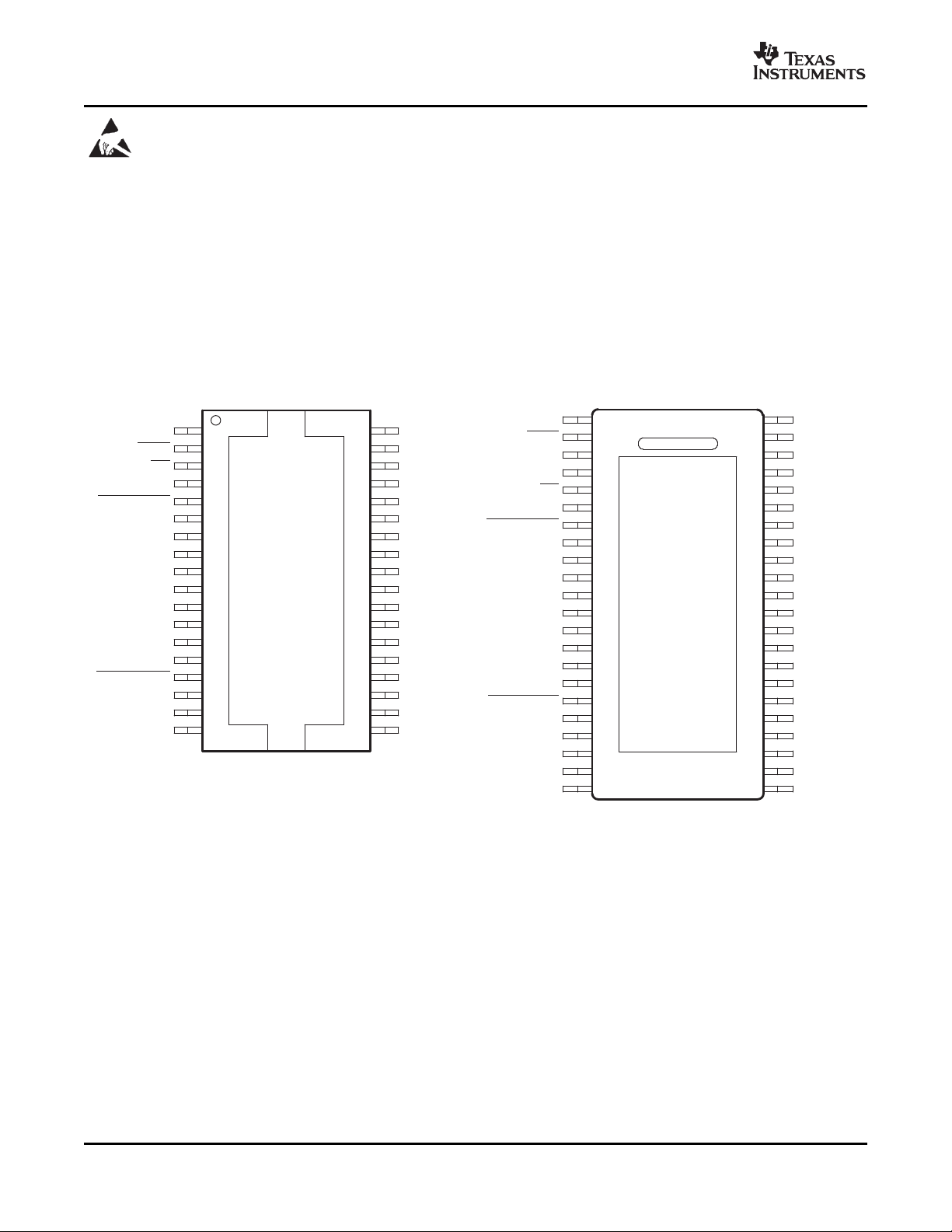
DKD PACKAGE
(TOP VIEW)
P0018-01
1
2
3
4
5
6
7
8
9
10
11
12
13
14
15
16
17
18
19
20
21
22
GVDD_B
OTW
NC
NC
SD
PWM_A
RESET_AB
PWM_B
OC_ADJ
GND
AGND
VREG
M3
M2
M1
PWM_C
RESET_CD
PWM_D
NC
NC
VDD
GVDD_C
DDV PACKAGE
(TOP VIEW)
GVDD_A
BST_A
NC
PVDD_A
PVDD_A
OUT_A
GND_A
GND_B
OUT_B
PVDD_B
BST_B
BST_C
PVDD_C
OUT_C
GND_C
GND_D
OUT_D
PVDD_D
PVDD_D
NC
BST_D
GVDD_D
44
43
42
41
40
39
38
37
36
35
34
33
32
31
30
29
28
27
26
25
24
23
P0016-02
TAS5162
SLES194C – OCTOBER 2006 – REVISED MAY 2007
These devices have limited built-in ESD protection. The leads should be shorted together or the device placed in conductive foam
during storage or handling to prevent electrostatic damage to the MOS gates.
GENERAL INFORMATION
Terminal Assignment
The TAS5162 is available in two thermally enhanced packages:
• 36-pin PSOP3 package (DKD)
• 44-pin HTSSOP PowerPad™ package (DDV)
Both package types contain a heat slug that is located on the top side of the device for convenient thermal
coupling to the heatsink.
2
Submit Documentation Feedback
www.ti.com
SLES194C – OCTOBER 2006 – REVISED MAY 2007
GENERAL INFORMATION (continued)
MODE Selection Pins for Both Packages
MODE PINS
M3 M2 M1
0 0 0 2N
0 0 1 2N
0 1 0 1N
0 1 1 1N
1 0 0 1N
1 0 1 Protection works similarly to SE Mode
1 1 0
1 1 1
(1) The 1N and 2N naming convention is used to indicate the required number of PWM lines to the power stage per channel in a specific
mode.
(2) An overload protection (OLP) occurring on A or B causes both channels to shut down. An OLP on C or D works similarly. Global errors
like overtemperature error (OTE), undervoltage protection (UVP), and power-on reset (POR) affect all channels.
PWM INPUT OUTPUT CONFIGURATION PROTECTION SCHEME
(1)
AD/BD modulation 2 channels BTL output BTL mode, full protection
(1)
AD/BD modulation 2 channels BTL output BTL mode, latching shutdown
(1)
AD modulation 2 channels BTL output BTL mode, full protection
(1)
AD modulation 1 channel PBTL output PBTL mode, full protection. Only PWM_A input
Protection works similarly to BTL mode
(1)
AD modulation 4 channels SE output
difference in SE mode is that OUT_X is Hi-Z
instead of a pulldown through internal pulldown
resistor.
(1)
1N
AD modulation PWM Input protection, latching
4 channels SE output - No
shutdown
(1,0,0); however, the PWM input protection is
disabled. Also, overcurrent detection will latch if
an error occurs.
Reserved
is used.
TAS5162
(2)
(2)
(2)
(2)
. Only
(2)
Package Heat Dissipation Ratings
(1)
PARAMETER TAS5162DKD TAS5162DDV
R
( ° C/W)—2 BTL or 4 SE channels (8 transistors) 1.0 1.1
θ JC
R
( ° C/W)—1 BTL or 2 SE channel(s) (4 transistors) 1.5 2.2
θ JC
R
( ° C/W)—(1 transistor) 5.0 7.4
θ JC
Pad area
(2)
2
80 mm
(1) JC is junction-to-case, CH is case-to-heatsink.
(2) R
is an important consideration. Assume a 2-mil thickness of typical thermal grease between the pad area and the heatsink and both
θ CH
channels active. The R
with this condition is 2.6 ° C/W for the DKD package and 4.0 ° C/W for the DDV package.
θ CH
2
34 mm
Submit Documentation Feedback
3
www.ti.com
TAS5162
SLES194C – OCTOBER 2006 – REVISED MAY 2007
ABSOLUTE MAXIMUM RATINGS
over operating free-air temperature range unless otherwise noted
TAS5162
VDD to AGND –0.3 V to 13.2 V
GVDD_X to AGND –0.3 V to 13.2 V
PVDD_X to GND_X
OUT_X to GND_X
BST_X to GND_X
VREG to AGND –0.3 V to 4.2 V
GND_X to GND –0.3 V to 0.3 V
GND_X to AGND –0.3 V to 0.3 V
GND to AGND –0.3 V to 0.3 V
PWM_X, OC_ADJ, M1, M2, M3 to AGND –0.3 V to 4.2 V
RESET_X, SD, OTW to AGND –0.3 V to 7 V
Maximum continuous sink current ( SD, OTW) 9 mA
Maximum operating junction temperature range, T
Storage temperature –40 ° C to 125 ° C
Lead temperature, 1,6 mm (1/16 inch) from case for 10 seconds 260 ° C
Minimum pulse duration, low 50 ns
(2)
(2)
(2)
J
(1)
–0.3 V to 71 V
–0.3 V to 71V
–0.3 V to 79.7 V
0 ° C to 125 ° C
(1) Stresses beyond those listed under "absolute maximum ratings" may cause permanent damage to the device. These are stress ratings
only, and functional operation of the device at these or any other conditions beyond those indicated under "recommended operating
conditions" is not implied. Exposure to absolute-maximum-rated conditions for extended periods may affect device reliability.
(2) These voltages represent the dc voltage + peak ac waveform measured at the terminal of the device in all conditions.
ORDERING INFORMATION
T
A
0 ° C to 70 ° C TAS5162DKD 36-pin PSOP3
0 ° C to 70 ° C TAS5162DDV 44-pin HTSSOP
PACKAGE DESCRIPTION
For the most current specification and package information, see the TI Web site at www.ti.com.
4
Submit Documentation Feedback
www.ti.com
SLES194C – OCTOBER 2006 – REVISED MAY 2007
Terminal Functions
TERMINAL
NAME DKD NO. DDV NO.
AGND 9 11 P Analog ground
BST_A 35 43 P HS bootstrap supply (BST), external .033- µ F capacitor to OUT_A
BST_B 28 34 P HS bootstrap supply (BST), external .033- µ F capacitor to OUT_B
BST_C 27 33 P HS bootstrap supply (BST), external .033- µ F capacitor to OUT_C
BST_D 20 24 P HS bootstrap supply (BST), external .033- µ F capacitor to OUT_D
GND 8 10 P Ground
GND_A 32 38 P Power ground for half-bridge A
GND_B 31 37 P Power ground for half-bridge B
GND_C 24 30 P Power ground for half-bridge C
GND_D 23 29 P Power ground for half-bridge D
GVDD_A 36 44 P Gate-drive voltage supply requires 0.1- µ F capacitor to AGND
GVDD_B 1 1 P Gate-drive voltage supply requires 0.1- µ F capacitor to AGND
GVDD_C 18 22 P Gate-drive voltage supply requires 0.1- µ F capacitor to AGND
GVDD_D 19 23 P Gate-drive voltage supply requires 0.1- µ F capacitor to AGND
M1 13 15 I Mode selection pin
M2 12 14 I Mode selection pin
M3 11 13 I Mode selection pin
NC – 3, 4, 19, 20, 25, – No connect. Pins may be grounded.
42
OC_ADJ 7 9 O Analog overcurrent programming pin requires resistor to ground
OTW 2 2 O Overtemperature warning signal, open-drain, active-low
OUT_A 33 39 O Output, half-bridge A
OUT_B 30 36 O Output, half-bridge B
OUT_C 25 31 O Output, half-bridge C
OUT_D 22 28 O Output, half-bridge D
PVDD_A 34 40, 41 P Power supply input for half-bridge A requires close decoupling of
PVDD_B 29 35 P Power supply input for half-bridge B requires close decoupling of
PVDD_C 26 32 P Power supply input for half-bridge C requires close decoupling of
PVDD_D 21 26, 27 P Power supply input for half-bridge D requires close decoupling of
PWM_A 4 6 I Input signal for half-bridge A
PWM_B 6 8 I Input signal for half-bridge B
PWM_C 14 16 I Input signal for half-bridge C
PWM_D 16 18 I Input signal for half-bridge D
RESET_AB 5 7 I Reset signal for half-bridge A and half-bridge B, active-low
RESET_CD 15 17 I Reset signal for half-bridge C and half-bridge D, active-low
SD 3 5 O Shutdown signal, open-drain, active-low
VDD 17 21 P Power supply for digital voltage regulator requires a 47- µ F
VREG 10 12 P Digital regulator supply filter pin requires 0.1- µ F capacitor to
(1) I = input, O = output, P = power
FUNCTION
(1)
required
required
required
required
0.01- µ F capacitor in parallel with a 1.0- µ F capacitor to GND_A.
0.01- µ F capacitor in parallel with a 1.0- µ F capacitor to GND_B.
0.01- µ F capacitor in parallel with a 1.0- µ F capacitor to GND_C.
0.01- µ F capacitor in parallel with a 1.0- µ F capacitor to GND_D.
capacitor in parallel with a 0.1- µ F capacitor to GND for decoupling.
AGND.
DESCRIPTION
TAS5162
Submit Documentation Feedback
5
www.ti.com
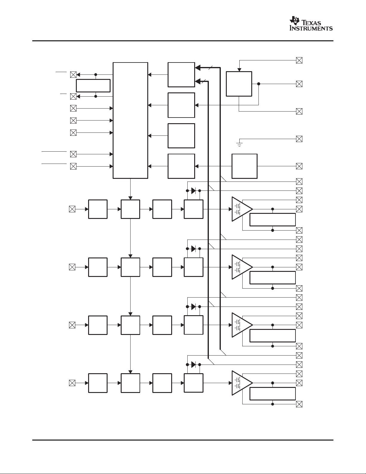
Temp.
Sense
M1
M2
RESET_AB
SD
OTW
AGND
OC_ADJ
VREG VREG
VDD
M3
Power
On
Reset
Under-
voltage
Protection
GND
PWM_D OUT_D
GND_D
PVDD_D
BST_D
Timing
Gate
Drive
PWM
Rcv.
Overload
Protection
I
sens e
GVDD_D
RESET_CD
4
Protection
and
I/OLogic
PWM_C OUT_C
GND_C
PVDD_C
BST_C
Timing
Gate
Drive
Ctrl.
PWM
Rcv.
GVDD_C
PWM_B OUT_B
GND_B
PVDD_B
BST_B
Timing
Gate
Drive
Ctrl.
PWM
Rcv.
GVDD_B
PWM_A OUT_A
GND_A
PVDD_A
BST_A
Timing
Gate
Drive
Ctrl.
PWM
Rcv.
GVDD_A
Ctrl.
BTL/PBTL−Configuration
Pulldown Resistor
BTL/PBTL−Configuration
PulldownResistor
BTL/PBTL−Configuration
PulldownResistor
BTL/PBTL−Configuration
PulldownResistor
InternalPullup
ResistorstoVREG
B0034-03
4
TAS5162
SLES194C – OCTOBER 2006 – REVISED MAY 2007
SYSTEM BLOCK DIAGRAM
Submit Documentation Feedback
6
www.ti.com
2nd-Order L-C
Output Filter
for Each
Half-Bridge
Bootstrap
Capacitors
2-Channel
H-Bridge
BTL Mode
System
Microcontroller
OUT_A
OUT_B
OUT_C
OUT_D
BST_A
BST_B
BST_C
BST_D
RESET_AB
RESET_CD
System
Power
Supply
Hardwire
Mode
Control
PVDD
GVDD (12 V)/VDD (12 V)
GND
Hardwire
OC Limit
M1
M3
PVDD
Power
Supply
Decoupling
50 V
12 V
GND
VAC
PWM_A
PWM_C
PWM_D
PWM_B
VALID
M2
Left-
Channel
Output
Right-
Channel
Output
Input
H-Bridge 1
Input
H-Bridge 2
GVDD
VDD
VREG
Power Supply
Decoupling
4
PVDD_A, B, C, D
GND_A, B, C, D
GVDD_A, B, C, D
4 4
VDD
GND
VREG
AGND
OC_ADJ
Bootstrap
Capacitors
2nd-Order L-C
Output Filter
for Each
Half-Bridge
SD
OTW
Output
H-Bridge 2
Output
H-Bridge 1
OTW
SD
TAS5508
B0047-01
TAS5162
SLES194C – OCTOBER 2006 – REVISED MAY 2007
FUNCTIONAL BLOCK DIAGRAM
Submit Documentation Feedback
7
www.ti.com
TAS5162
SLES194C – OCTOBER 2006 – REVISED MAY 2007
RECOMMENDED OPERATING CONDITIONS
MIN TYP MAX UNIT
PVDD_X Half-bridge supply DC supply voltage 0 50 52.5 V
GVDD_X DC supply voltage 10.8 12 13.2 V
VDD Digital regulator input DC supply voltage 10.8 12 13.2 V
RL(BTL) 4.6 6-8
RL(SE) Load impedance Output AD modulation, switching 2.5 3-8 Ω
RL(PBTL) 4-8
L
(BTL) 5 10
Output
L
(SE) Output-filter inductance 5 10 µ H
Output
L
(PBTL) 5 10
Output
F
PWM
T
J
AUDIO SPECIFICATIONS (BTL)
PVDD_X = 50 V, GVDD = VDD = 12 V, BTL mode, RL= 6 Ω , R
384 kHz, case temperature = 75 ° C, unless otherwise noted. Audio performance is recorded as a chipset, using TAS5508
PWM processor with an effective modulation index limit of 96.1%. All performance is in accordance with recommended
operating conditions unless otherwise specified.
P
O
THD+N Total harmonic distortion + noise
V
n
SNR Signal-to-noise ratio
DNR Dynamic range dB
P
idle
(1) SNR is calculated relative to 0-dBFS input level.
(2) Actual system idle losses are affected by core losses of output inductors.
Supply for logic regulators and gate-drive
circuitry
Output filter: L = 10 µ H, C = 470 nF.
frequency > 350 kHz
Minimum output inductance under
short-circuit condition
PWM frame rate 192 384 432 kHz
Junction temperature 0 125 ° C
= 22 K Ω , audio frequency = 1 kHz, AES17 filter, F
OC
PARAMETER TEST CONDITIONS UNIT
RL= 4 Ω , 10% THD, clipped input
signal (PVDD = 38.5 Volts)
RL= 6 Ω , 10% THD, clipped input
signal
RL= 8 Ω , 10% THD, clipped input
Power output per channel, DKD package
signal
RL= 4 Ω , 0 dBFS, unclipped input
signal (PVDD = 38.5 Volts)
RL= 6 Ω , 0 dBFS, unclipped input
signal
RL= 8 Ω , 0 dBFS, unclipped input
signal
TAS5162
MIN TYP MAX
160
210
160 W
120
165
125
0 dBFS 0.2%
1 W 0.09%
Output integrated noise A-weighted, TAS5508 Modulator 140 µ V
A-Weighted, TAS5518 Modulator 85
(1)
A-weighted, TAS5508 Modulator 102
A-weighted, TAS5518 Modulator 112
A-weighted, input level = –60 dBFS
using TAS5508 modulator
A-weighted, input level = –60 dBFS
using TAS5518 modulator
Power dissipation due to idle losses (IPVDD_X) PO= 0 W, 4 channels switching
(2)
102
112
2.5 W
=
PWM
dB
AUDIO SPECIFICATIONS (Single-Ended Output)
PVDD_X = 50 V, GVDD = VDD = 12 V, SE mode, RL= 3 Ω , R
384 kHz, case temperature = 75 ° C, unless otherwise noted. Audio performance is recorded as a chipset, using TAS5086
PWM processor with an effective modulation index limit of 96.1%. All performance is in accordance with recommended
8
Submit Documentation Feedback
= 22 K Ω , audio frequency = 1 kHz, AES17 filter, F
OC
=
PWM
www.ti.com
TAS5162
SLES194C – OCTOBER 2006 – REVISED MAY 2007
AUDIO SPECIFICATIONS (Single-Ended Output) (continued)
PVDD_X = 50 V, GVDD = VDD = 12 V, SE mode, RL= 3 Ω , R
384 kHz, case temperature = 75 ° C, unless otherwise noted. Audio performance is recorded as a chipset, using TAS5086
PWM processor with an effective modulation index limit of 96.1%. All performance is in accordance with recommended
operating conditions unless otherwise specified.
operating conditions unless otherwise specified.
PARAMETER TEST CONDITIONS UNIT
P
O
THD+N Total harmonic distortion + noise
V
n
SNR Signal-to-noise ratio
DNR Dynamic range 110 dB
P
idle
(1) SNR is calculated relative to 0-dBFS input level.
(2) Actual system idle losses are affected by core losses of output inductors.
Power output per channel, DKD package W
Output integrated noise A-weighted 85 µ V
(1)
Power dissipation due to idle losses (IPVDD_X) PO= 0 W, 4 channels switching
= 22 K Ω , audio frequency = 1 kHz, AES17 filter, F
OC
TAS5162
MIN TYP MAX
RL= 3 Ω , 10% THD, clipped input
signal
RL= 4 Ω , 10% THD, clipped input
signal
RL= 3 Ω , 0 dBFS, unclipped input
signal
RL= 4 Ω , 0 dBFS, unclipped input
signal
105
80
80
60
0 dBFS 0.2%
1 W 0.09%
A-weighted 110 dB
A-weighted, input level = –60 dBFS
using TAS5086 modulator
(2)
2.5 W
=
PWM
AUDIO SPECIFICATIONS (PBTL)
PVDD_X = 50 V, GVDD = VDD = 12 V, PBTL mode, RL= 4 Ω , R
Schottky diode connected from each output pin to to ground, audio frequency = 1 kHz, AES17 filter, F
temperature = 75 ° C, unless otherwise noted. Audio performance is recorded as a chipset, using TAS5508 PWM processor
with an effective modulation index limit of 96.1%. All performance is in accordance with recommended operating conditions
unless otherwise specified.
PARAMETER TEST CONDITIONS UNIT
P
O
THD+N Total harmonic distortion + noise
V
n
SNR Signal-to-noise ratio
DNR Dynamic range dB
P
idle
(1) SNR is calculated relative to 0-dBFS input level.
(2) Actual system idle losses are affected by core losses of output inductors.
Power output per channel, DKD package W
Output integrated noise A-weighted 140 µ V
(1)
Power dissipation due to idle losses (IPVDD_X) PO= 0 W, 1 channel switching
= 22 K Ω , 1/2 of an MBRM5100-13 dual, 5A@100V,
OC
PWM
= 384 kHz, case
TAS5162
MIN TYP MAX
RL= 4 Ω , 10% THD, clipped input
signal
RL= 4 Ω , 0 dBFS, unclipped input
signal
RL= 3 Ω , 10% THD, clipped input
signal
RL= 3 Ω , 0 dBFS, unclipped input
signal
300
240
400
300
0 dBFS 0.2%
1 W 0.09%
A-weighted 102 dB
A-weighted, input level = –60 dBFS
using TAS5508 modulator
A-weighted, input level = –60 dBFS
using TAS5518 modulator
(2)
102
110
2.5 W
Submit Documentation Feedback
9
 Loading...