

Page 1
TM
www.ti.com
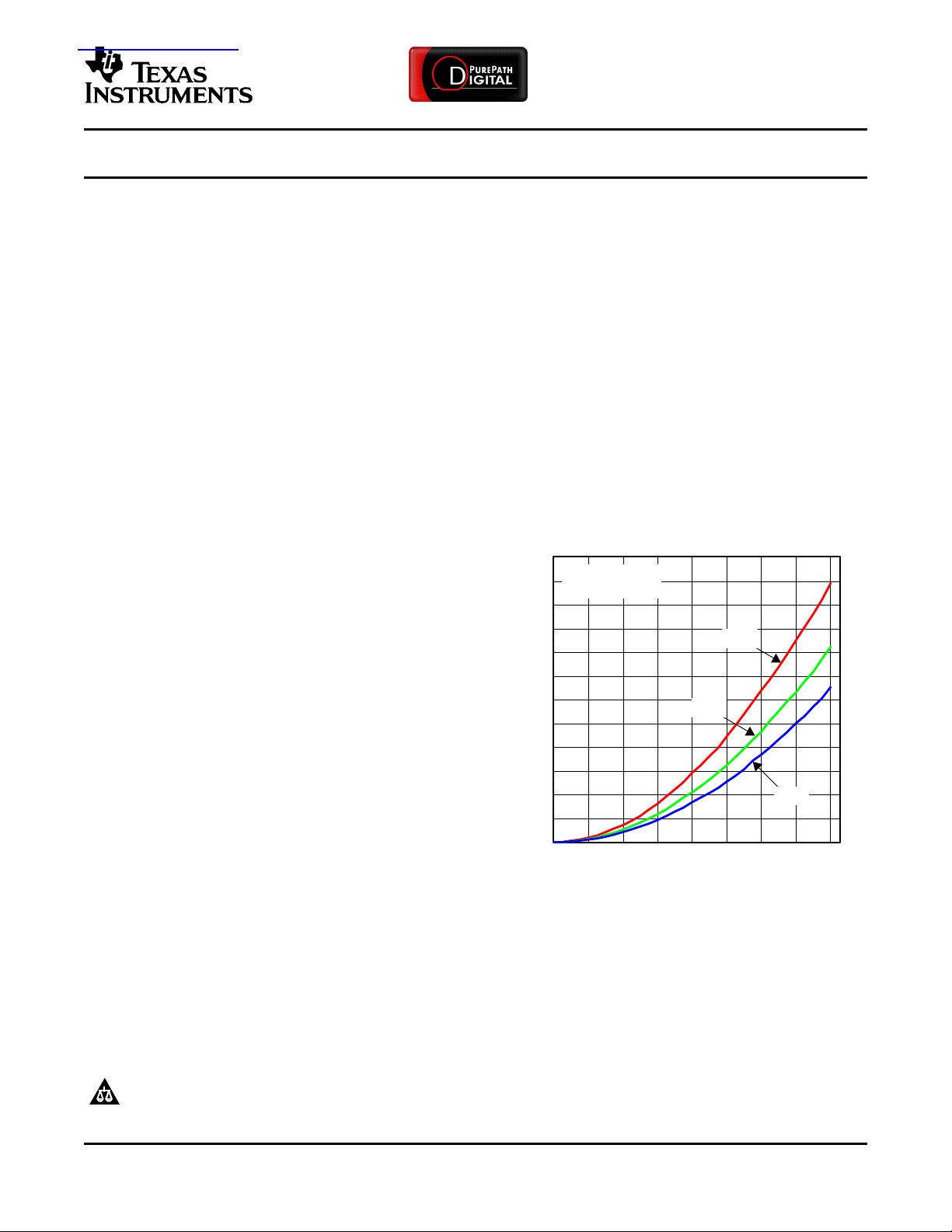
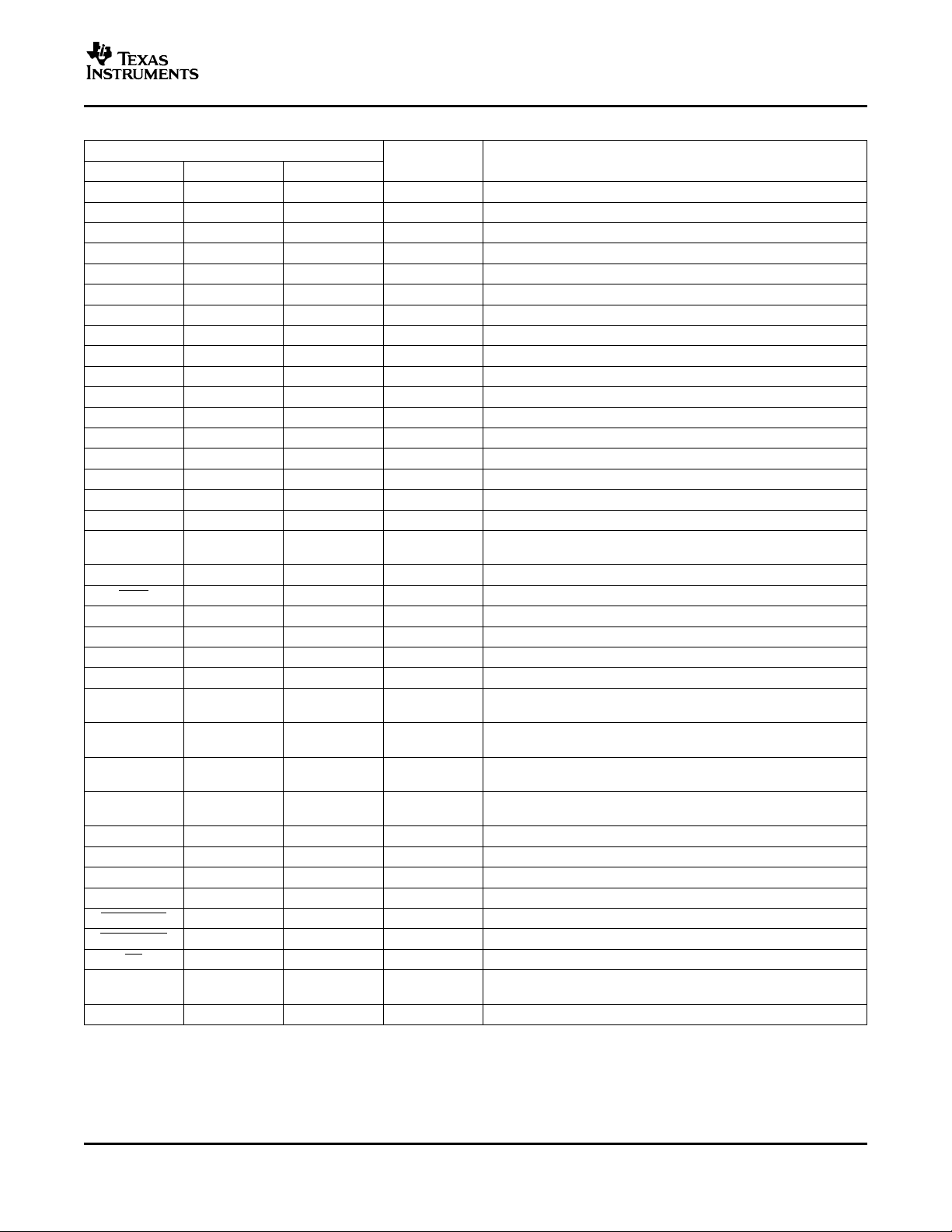
PVDD − Supply Voltage − V
0
10
20
30
40
50
60
70
80
90
100
110
120
0 4 8 12 16 20 24 28 32
P
O
− Output Power − W
8 Ω
4 Ω
TC = 75°C
THD+N @ 10%
6 Ω
G002
查询TAS5142供应商
TAS5142
SLES126B – DECEMBER 2004 – REVISED MAY 2005
STEREO DIGITAL AMPLIFIER POWER STAGE
FEATURES
• 2×100 W at 10% THD+N Into 4- Ω BTL
• 2×80 W at 10% THD+N Into 6- Ω BTL
• 2×65 W at 10% THD+N Into 8- Ω BTL
• 4×40 W at 10% THD+N Into 3- Ω SE
• 4×30 W at 10% THD+N Into 4- Ω SE
• 1×160 W at 10% THD+N Into 3- Ω PBTL
• 1×200 W at 10% THD+N Into 2- Ω PBTL
• >100 dB SNR (A-Weighted)
• <0.1% THD+N at 1 W
• Two Thermally Enhanced Package Options:
– DKD (36-pin PSOP3)
– DDV (44-pin HTSSOP)
• High-Efficiency Power Stage (>90%) With
140-m Ω Output MOSFETs
• Power-On Reset for Protection on Power Up
Without Any Power-Supply Sequencing
• Integrated Self-Protection Circuits Including
Undervoltage, Overtemperature, Overload,
Short Circuit
• Error Reporting
• EMI Compliant When Used With
Recommended System Design
• Intelligent Gate Drive
deliver high-quality, high-efficiency audio amplification
(1)
with proven EMI compliance. This device requires two
power supplies, at 12 V for GVDD and VDD, and at
32 V for PVDD. The TAS5142 does not require
power-up sequencing due to internal power-on reset.
The efficiency of this digital amplifier is greater than
90% into 6 Ω , which enables the use of smaller
power supplies and heatsinks.
(1)
The TAS5142 has an innovative protection system
integrated on-chip, safeguarding the device against a
wide range of fault conditions that could damage the
system. These safeguards are short-circuit protection,
overcurrent protection, undervoltage protection, and
overtemperature protection. The TAS5142 has a new
proprietary current-limiting circuit that reduces the
possibility of device shutdown during high-level music
transients. A new programmable overcurrent detector
allows the use of lower-cost inductors in the demodulation output filter.
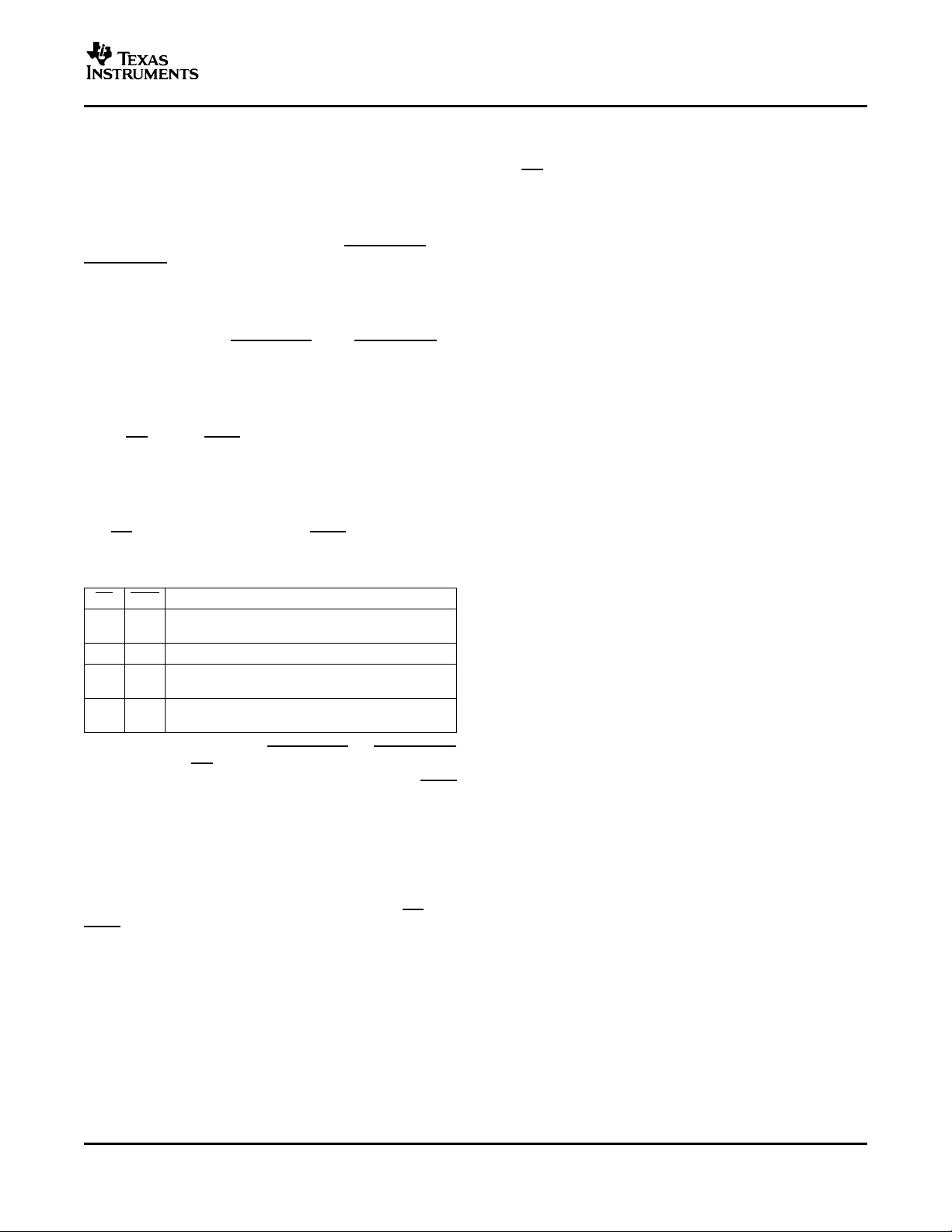
BTL OUTPUT POWER vs SUPPLY VOLTAGE
APPLICATIONS
• Mini/Micro Audio System
• DVD Receiver
• Home Theater
DESCRIPTION
The TAS5142 is a third-generation, high-performance, integrated stereo digital amplifier power stage
with an improved protection system. The TAS5142 is
capable of driving a 4- Ω bridge-tied load (BTL) at up
to 100 W per channel with low integrated noise at the
output, low THD+N performance, and low idle power
dissipation.
A low-cost, high-fidelity audio system can be built
using a TI chipset, comprising a modulator (e.g.,
TAS5508) and the TAS5142. This system only requires a simple passive LC demodulation filter to
PurePath Digital, PowerPad are trademarks of Texas Instruments.
All trademarks are the property of their respective owners.
PRODUCTION DATA information is current as of publication date.
Products conform to specifications per the terms of the Texas
Instruments standard warranty. Production processing does not
necessarily include testing of all parameters.
Please be aware that an important notice concerning availability, standard warranty, and use in critical applications of Texas
Instruments semiconductor products and disclaimers thereto appears at the end of this data sheet.
(1) It is not recommended to drive 200 W (total
power) into the DDV package continuously.
For multichannel systems that require two
channels to be driven at full power with the
DDV package option, it is recommended to
design the system so that the two channels
are in two separate devices.
PurePath Digital™
Copyright © 2004–2005, Texas Instruments Incorporated
Page 2
www.ti.com
1
2
3
4
5
6
7
8
9
10
11
12
13
14
15
16
17
18
36
35
34
33
32
31
30
29
28
27
26
25
24
23
22
21
20
19
GVDD_B
OTW
SD
PWM_A
RESET_AB
PWM_B
OC_ADJ
GND
AGND
VREG
M3
M2
M1
PWM_C
RESET_CD
PWM_D
VDD
GVDD_C
GVDD_A
BST_A
PVDD_A
OUT_A
GND_A
GND_B
OUT_B
PVDD_B
BST_B
BST_C
PVDD_C
OUT_C
GND_C
GND_D
OUT_D
PVDD_D
BST_D
GVDD_D
DKD PACKAGE
(TOP VIEW)
P0018-01
1
2
3
4
5
6
7
8
9
10
11
12
13
14
15
16
17
18
19
20
21
22
GVDD_B
OTW
NC
NC
SD
PWM_A
RESET_AB
PWM_B
OC_ADJ
GND
AGND
VREG
M3
M2
M1
PWM_C
RESET_CD
PWM_D
NC
NC
VDD
GVDD_C
DDV PACKAGE
(TOP VIEW)
GVDD_A
BST_A
NC
PVDD_A
PVDD_A
OUT_A
GND_A
GND_B
OUT_B
PVDD_B
BST_B
BST_C
PVDD_C
OUT_C
GND_C
GND_D
OUT_D
PVDD_D
PVDD_D
NC
BST_D
GVDD_D
44
43
42
41
40
39
38
37
36
35
34
33
32
31
30
29
28
27
26
25
24
23
P0016-02
TAS5142
SLES126B – DECEMBER 2004 – REVISED MAY 2005
These devices have limited built-in ESD protection. The leads should be shorted together or the device
placed in conductive foam during storage or handling to prevent electrostatic damage to the MOS gates.
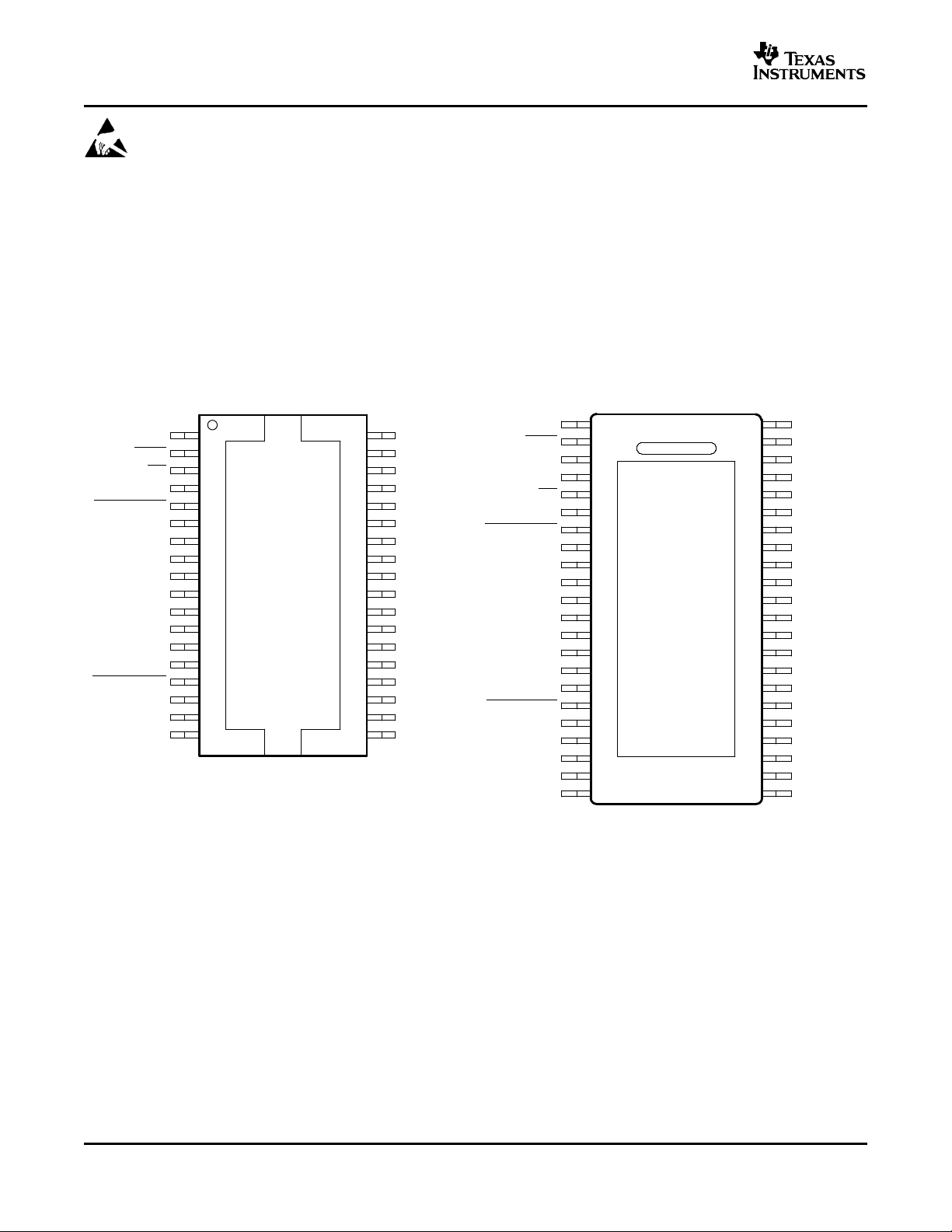
GENERAL INFORMATION
Terminal Assignment
The TAS5142 is available in two thermally enhanced packages:
• 36-pin PSOP3 package (DKD)
• 44-pin HTSSOP PowerPad™ package (DDV)
Both package types contain a heat slug that is located on the top side of the device for convenient thermal
coupling to the heatsink.
2
Page 3
www.ti.com
SLES126B – DECEMBER 2004 – REVISED MAY 2005
GENERAL INFORMATION (continued)
MODE Selection Pins for Both Packages
MODE PINS
M3 M2 M1
0 0 0 2N
0 0 1 Reserved
0 1 0 1N
0 1 1 1N
1 0 0 1N
1 0 1
1 1 0 Reserved
1 1 1
(1) The 1N and 2N naming convention is used to indicate the required number of PWM lines to the power stage per channel in a specific
mode.
(2) An overload protection (OLP) occurring on A or B causes both channels to shut down. An OLP on C or D works similarly. Global errors
like overtemperature error (OTE), undervoltage protection (UVP), and power-on reset (POR) affect all channels.
PWM INPUT OUTPUT CONFIGURATION PROTECTION SCHEME
(1)
AD/BD modulation 2 channels BTL output BTL mode
(1)
AD modulation 2 channels BTL output BTL mode
(1)
AD modulation 1 channel PBTL output PBTL mode. Only PWM_A input is used.
Protection works similarly to BTL mode
(1)
AD modulation 4 channels SE output
difference in SE mode is that OUT_X is Hi-Z
instead of a pulldown through internal pulldown
resistor.
(2)
(2)
TAS5142
(2)
. Only
Package Heat Dissipation Ratings
(1)
PARAMETER TAS5142DKD TAS5142DDV
R
(°C/W)—2 BTL or 4 SE channels (8 transistors) 1.28 1.28
θ JC
R
(°C/W)—1 BTL or 2 SE channel(s) (4 transistors) 2.56 2.56
θ JC
R
(°C/W)—(1 transistor) 8.6 8.6
θ JC
Pad area
(2)
2
80 mm
(1) JC is junction-to-case, CH is case-to-heatsink.
(2) R
is an important consideration. Assume a 2-mil thickness of typical thermal grease between the pad area and the heatsink. The
θ CH
R
with this condition is 0.8°C/W for the DKD package and 1.8°C/W for the DDV package.
θ CH
2
36 mm
3
Page 4
www.ti.com
TAS5142
SLES126B – DECEMBER 2004 – REVISED MAY 2005
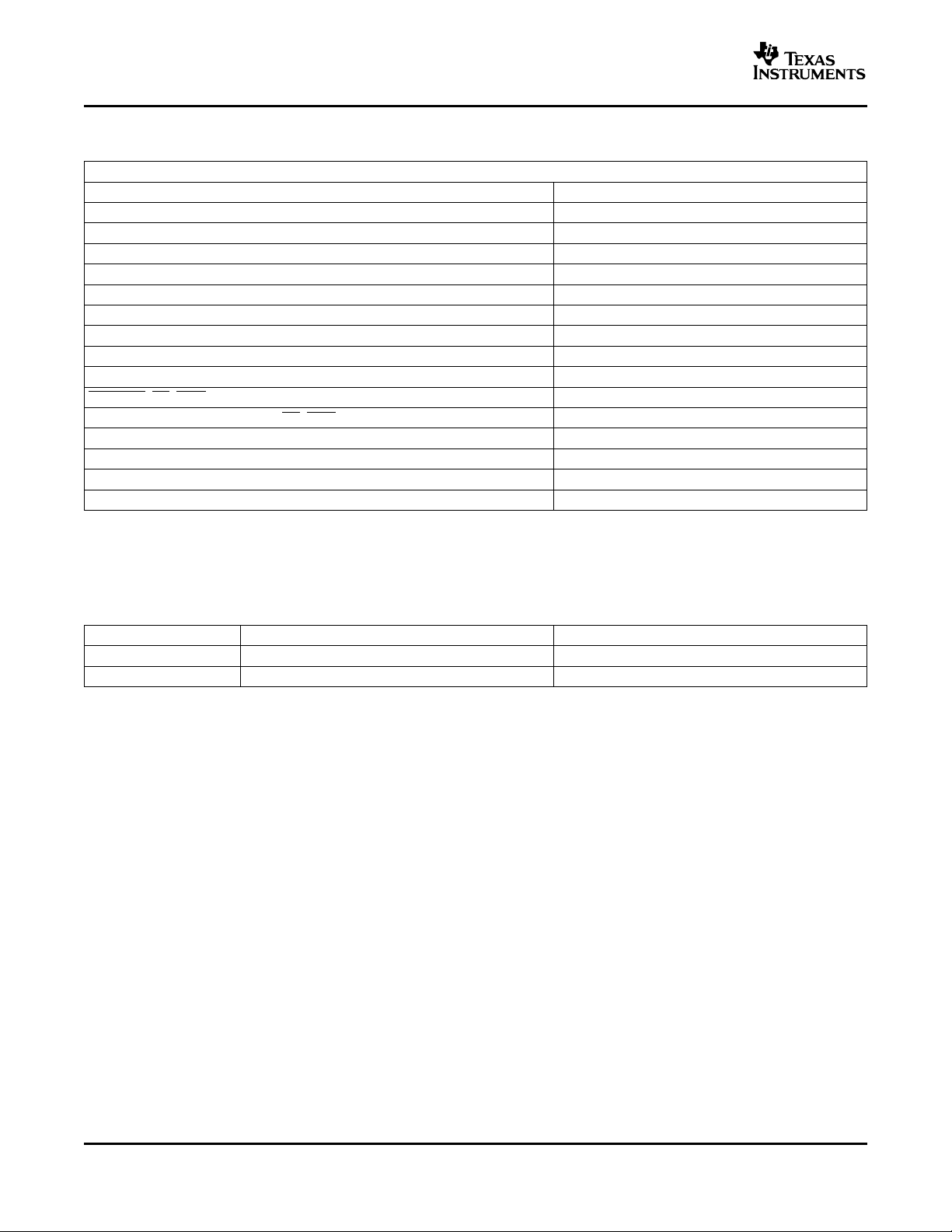
ABSOLUTE MAXIMUM RATINGS
over operating free-air temperature range unless otherwise noted
VDD to AGND –0.3 V to 13.2 V
GVDD_X to AGND –0.3 V to 13.2 V
PVDD_X to GND_X
OUT_X to GND_X
BST_X to GND_X
VREG to AGND –0.3 V to 4.2 V
GND_X to GND –0.3 V to 0.3 V
GND_X to AGND –0.3 V to 0.3 V
GND to AGND –0.3 V to 0.3 V
PWM_X, OC_ADJ, M1, M2, M3 to AGND –0.3 V to 4.2 V
RESET_X, SD, OTW to AGND –0.3 V to 7 V
Maximum continuous sink current ( SD, OTW) 9 mA
Maximum operating junction temperature range, T
Storage temperature –40°C to 125°C
Lead temperature, 1,6 mm (1/16 inch) from case for 10 seconds 260°C
Minimum pulse duration, low 50 ns
(2)
(2)
(2)
J
(1)
TAS5142
–0.3 V to 50 V
–0.3 V to 50 V
–0.3 V to 63.2 V
0°C to 125°C
(1) Stresses beyond those listed under "absolute maximum ratings" may cause permanent damage to the device. These are stress ratings
only, and functional operation of the device at these or any other conditions beyond those indicated under "recommended operating
conditions" is not implied. Exposure to absolute-maximum-rated conditions for extended periods may affect device reliability.
(2) These voltages represent the dc voltage + peak ac waveform measured at the terminal of the device in all conditions.
ORDERING INFORMATION
T
A
0°C to 70°C TAS5146DKD 36-pin PSOP3
0°C to 70°C TAS5142DDV 44-pin HTSSOP
PACKAGE DESCRIPTION
For the most current specification and package information, see the TI Web site at www.ti.com.
4
Page 5
www.ti.com
SLES126B – DECEMBER 2004 – REVISED MAY 2005
Terminal Functions
TERMINAL
NAME DKD NO. DDV NO.
AGND 9 11 P Analog ground
BST_A 35 43 P HS bootstrap supply (BST), external capacitor to OUT_A required
BST_B 28 34 P HS bootstrap supply (BST), external capacitor to OUT_B required
BST_C 27 33 P HS bootstrap supply (BST), external capacitor to OUT_C required
BST_D 20 24 P HS bootstrap supply (BST), external capacitor to OUT_D required
GND 8 10 P Ground
GND_A 32 38 P Power ground for half-bridge A
GND_B 31 37 P Power ground for half-bridge B
GND_C 24 30 P Power ground for half-bridge C
GND_D 23 29 P Power ground for half-bridge D
GVDD_A 36 44 P Gate-drive voltage supply requires 0.1- µ F capacitor to AGND
GVDD_B 1 1 P Gate-drive voltage supply requires 0.1- µ F capacitor to AGND
GVDD_C 18 22 P Gate-drive voltage supply requires 0.1- µ F capacitor to AGND
GVDD_D 19 23 P Gate-drive voltage supply requires 0.1- µ F capacitor to AGND
M1 13 15 I Mode selection pin
M2 12 14 I Mode selection pin
M3 11 13 I Mode selection pin
NC – 3, 4, 19, 20, 25, – No connect. Pins may be grounded.
42
OC_ADJ 7 9 O Analog overcurrent programming pin requires resistor to ground
OTW 2 2 O Overtemperature warning signal, open-drain, active-low
OUT_A 33 39 O Output, half-bridge A
OUT_B 30 36 O Output, half-bridge B
OUT_C 25 31 O Output, half-bridge C
OUT_D 22 28 O Output, half-bridge D
PVDD_A 34 40, 41 P Power supply input for half-bridge A requires close decoupling of
PVDD_B 29 35 P Power supply input for half-bridge B requires close decoupling of
PVDD_C 26 32 P Power supply input for half-bridge C requires close decoupling of
PVDD_D 21 26, 27 P Power supply input for half-bridge D requires close decoupling of
PWM_A 4 6 I Input signal for half-bridge A
PWM_B 6 8 I Input signal for half-bridge B
PWM_C 14 16 I Input signal for half-bridge C
PWM_D 16 18 I Input signal for half-bridge D
RESET_AB 5 7 I Reset signal for half-bridge A and half-bridge B, active-low
RESET_CD 15 17 I Reset signal for half-bridge C and half-bridge D, active-low
SD 3 5 O Shutdown signal, open-drain, active-low
VDD 17 21 P Power supply for digital voltage regulator requires 0.1- µ F capacitor
VREG 10 12 P Digital regulator supply filter pin requires 0.1- µ F capacitor to AGND.
(1) I = input, O = output, P = power
FUNCTION
(1)
DESCRIPTION
0.1- µ F capacitor to GND_A.
0.1- µ F capacitor to GND_B.
0.1- µ F capacitor to GND_C.
0.1- µ F capacitor to GND_D.
to GND.
TAS5142
5
Page 6
www.ti.com
2nd-Order L-C
Output Filter
for Each
Half-Bridge
Bootstrap
Capacitors
2-Channel
H-Bridge
BTL Mode
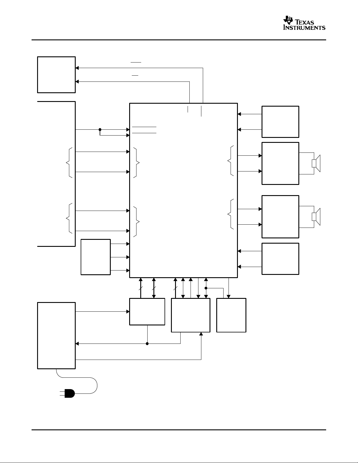
System
Microcontroller
OUT_A
OUT_B
OUT_C
OUT_D
BST_A
BST_B
BST_C
BST_D
RESET_AB
RESET_CD
System
Power
Supply
Hardwire
Mode
Control
PVDD
GVDD (12 V)/VDD (12 V)
GND
Hardwire
OC Limit
M1
M3
PVDD
Power
Supply
Decoupling
32 V
12 V
GND
VAC
PWM_A
PWM_C
PWM_D
PWM_B
VALID
M2
Left-
Channel
Output
Right-
Channel
Output
Input
H-Bridge 1
Input
H-Bridge 2
GVDD
VDD
VREG
Power Supply
Decoupling
4
PVDD_A, B, C, D
GND_A, B, C, D
GVDD_A, B, C, D
4 4
VDD
GND
VREG
AGND
OC_ADJ
Bootstrap
Capacitors
2nd-Order L-C
Output Filter
for Each
Half-Bridge
SD
OTW
Output
H-Bridge 2
Output
H-Bridge 1
OTW
SD
TAS5508
B0047-01
TAS5142
SLES126B – DECEMBER 2004 – REVISED MAY 2005
SYSTEM BLOCK DIAGRAM
6
Page 7
www.ti.com
Temp.
Sense
M1
M2
RESET_AB
SD
OTW
AGND
OC_ADJ
VREG VREG
VDD
M3
Power
On
Reset
Under-
voltage
Protection
GND
PWM_D OUT_D
GND_D
PVDD_D
BST_D
Timing
Gate
Drive
PWM
Rcv.
Overload
Protection
I
sense
GVDD_D
RESET_CD
4
Protection
and
I/O Logic
PWM_C OUT_C
GND_C
PVDD_C
BST_C
Timing
Gate
Drive
Ctrl.
PWM
Rcv.
GVDD_C
PWM_B OUT_B
GND_B
PVDD_B
BST_B
Timing
Gate
Drive
Ctrl.
PWM
Rcv.
GVDD_B
PWM_A OUT_A
GND_A
PVDD_A
BST_A
Timing
Gate
Drive
Ctrl.
PWM
Rcv.
GVDD_A
Ctrl.
BTL/PBTL−Configuration
Pulldown Resistor
BTL/PBTL−Configuration
Pulldown Resistor
BTL/PBTL−Configuration
Pulldown Resistor
BTL/PBTL−Configuration
Pulldown Resistor
Internal Pullup
Resistors to VREG
B0034-02
FUNCTIONAL BLOCK DIAGRAM
TAS5142
SLES126B – DECEMBER 2004 – REVISED MAY 2005
7
Page 8
www.ti.com
TAS5142
SLES126B – DECEMBER 2004 – REVISED MAY 2005
RECOMMENDED OPERATING CONDITIONS
MIN TYP MAX UNIT
PVDD_X Half-bridge supply DC supply voltage 0 32 34 V
GVDD_X DC supply voltage 10.8 12 13.2 V
VDD Digital regulator input DC supply voltage 10.8 12 13.2 V
RL(BTL) 3 4
RL(SE) Load impedance Output AD modulation, switching fre- 2 3 Ω
RL(PBTL) 1.5 2
L
(BTL) 5 10
Output
L
(SE) Output-filter inductance 5 10 µ H
Output
L
(PBTL) 5 10
Output
F
PWM
T
J
AUDIO SPECIFICATIONS (BTL)
PVDD_X = 32 V, GVDD = VDD = 12 V, BTL mode, RL= 4 Ω , audio frequency = 1 kHz, AES17 filter, F
temperature = 75°C, unless otherwise noted. Audio performance is recorded as a chipset, using TAS5508 PWM processor
with an effective modulation index limit of 96.1%. All performance is in accordance with recommended operating conditions
unless otherwise specified.
P
O
THD+N Total harmonic distortion + noise
V
n
SNR Signal-to-noise ratio
DNR Dynamic range dB
P
idle
(1) SNR is calculated relative to 0-dBFS input level.
(2) Actual system idle losses are affected by core losses of output inductors.
Supply for logic regulators and gate-drive
circuitry
Output filter: L = 10 µ H, C = 470 nF.
quency > 350 kHz
Minimum output inductance under
short-circuit condition
PWM frame rate 192 384 432 kHz
Junction temperature 0 125 °C
= 384 kHz, case
PWM
PARAMETER TEST CONDITIONS UNIT
Power output per channel, DKD package
RL= 4 Ω , 10% THD, clipped input
signal
RL= 6 Ω , 10% THD, clipped input
signal
RL= 8 Ω , 10% THD, clipped input
signal
RL= 4 Ω , 0 dBFS, unclipped input
signal
RL= 6 Ω , 0 dBFS, unclipped input
signal
RL= 8 Ω , 0 dBFS, unclipped input
signal
TAS5142
MIN TYP MAX
100
80
65 W
80
60
50
0 dBFS 0.3%
1 W 0.1%
Output integrated noise A-weighted 140 µ V
(1)
Power dissipation due to idle losses (IPVDD_X) PO= 0 W, 4 channels switching
A-weighted 102 dB
A-weighted, input level = –60 dBFS
using TAS5508 modulator
A-weighted, input level = –60 dBFS
using TAS5518 modulator
(2)
102
110
2 W
8
Page 9

www.ti.com
SLES126B – DECEMBER 2004 – REVISED MAY 2005
AUDIO SPECIFICATIONS (Single-Ended Output)
PVDD_X = 32 V, GVDD = VDD = 12 V, SE mode, RL= 4 Ω , audio frequency = 1 kHz, AES17 filter, F
temperature = 75°C, unless otherwise noted. Audio performance is recorded as a chipset, using TAS5086 PWM processor
with an effective modulation index limit of 96.1%. All performance is in accordance with recommended operating conditions
unless otherwise specified.
PARAMETER TEST CONDITIONS UNIT
RL= 3 Ω , 10% THD, clipped input
signal
RL= 4 Ω , 10% THD, clipped input
P
O
Power output per channel, DKD package W
signal
RL= 3 Ω , 0 dBFS, unclipped input
signal
RL= 4 Ω , 0 dBFS, unclipped input
signal
THD+N Total harmonic distortion + noise
V
n
SNR Signal-to-noise ratio
Output integrated noise A-weighted 90 µ V
(1)
DNR Dynamic range 100 dB
P
idle
Power dissipation due to idle losses (IPVDD_X) PO= 0 W, 4 channels switching
0 dBFS 0.2%
1 W 0.1%
A-weighted 100 dB
A-weighted, input level = –60 dBFS
using TAS5508 modulator
(2)
(1) SNR is calculated relative to 0-dBFS input level.
(2) Actual system idle losses are affected by core losses of output inductors.
MIN TYP MAX
PWM
TAS5142
= 384 kHz, case
40
30
30
20
2 W
TAS5142
AUDIO SPECIFICATIONS (PBTL)
PVDD_X = 32 V, GVDD = VDD = 12 V, PBTL mode, RL= 3 Ω , audio frequency = 1 kHz, AES17 filter, F
temperature = 75°C, unless otherwise noted. Audio performance is recorded as a chipset, using TAS5508 PWM processor
with an effective modulation index limit of 96.1%. All performance is in accordance with recommended operating conditions
unless otherwise specified.
PARAMETER TEST CONDITIONS UNIT
RL= 3 Ω , 10% THD, clipped input
signal
RL= 2 Ω , 10% THD, clipped input
P
O
Power output per channel, DKD package W
signal
RL= 3 Ω , 0 dBFS, unclipped input
signal
RL= 2 Ω , 0 dBFS, unclipped input
signal
THD+N Total harmonic distortion + noise
V
n
Output integrated noise A-weighted 140 µ V
SNR Signal-to-noise ratio
(1)
0 dBFS 0.2%
1 W 0.1%
A-weighted 102 dB
A-weighted, input level = –60 dBFS
DNR Dynamic range dB
using TAS5508 modulator
A-weighted, input level = –60 dBFS
using TAS5518 modulator
P
idle
Power dissipation due to idle losses (IPVDD_X) PO= 0 W, 1 channel switching
(2)
(1) SNR is calculated relative to 0-dBFS input level.
(2) Actual system idle losses are affected by core losses of output inductors.
MIN TYP MAX
PWM
TAS5142
= 384 kHz, case
160
200
120
150
102
110
2 W
9
Page 10

www.ti.com
TAS5142
SLES126B – DECEMBER 2004 – REVISED MAY 2005
ELECTRICAL CHARACTERISTICS
RL= 4 Ω , F
unless otherwise specified.
Internal Voltage Regulator and Current Consumption
VREG VDD = 12 V 3 3.3 3.6 V
IVDD VDD supply current mA
IGVDD_X Gate supply current per half-bridge mA
IPVDD_X Half-bridge idle current
Output Stage MOSFETs
R
DSon,LS
R
DSon,HS
I/O Protection
V
uvp,G
V
uvp,hyst
(1)
OTW
OTW
HYST
(1)
OTE
OTE-
OTW
differential
OTE
HYST
OLPC Overload protection counter F
I
OC
I
OCT
R
OCP
R
PD
Static Digital Specifications
V
IH
V
IL
Leakage Input leakage current –10 10 µ A
OTW/SHUTDOWN (SD)
R
INT_PU
V
OH
V
OL
FANOUT Device fanout OTW, SD No external pullup 30 Devices
= 384 kHz, unless otherwise noted. All performance is in accordance with recommended operating conditions
PWM
PARAMETER TEST CONDITIONS UNIT
Voltage regulator, only used as a
reference node
Operating, 50% duty cycle 7 17
Idle, reset mode 6 11
50% duty cycle 5 16
Reset mode 0.3 1
50% duty cycle, without output filter or load 15 25 mA
Reset mode, no switching 7 25 µ A
Drain-to-source resistance, LS 140 155 m Ω
Drain-to-source resistance, HS 140 155 m Ω
TJ= 25°C, includes metallization resistance,
GVDD = 12 V
TJ= 25°C, includes metallization resistance,
GVDD = 12 V
Undervoltage protection limit,
GVDD_X
(1)
Overtemperature warning 115 125 135 °C
(1)
Temperature drop needed below
OTW temp. for OTW to be inactive 25 °C
after the OTW event
Overtemperature error 145 155 165 °C
OTE-OTW differential 30 °C
(1)
(1)
A reset event must occur for SD to
be released following an OTE event.
= 384 kHz 1.25 ms
PWM
Overcurrent limit protection 7.9 9.7 11.4 A
Resistor—programmable, high-end,
R
= 18 k Ω
OCP
Overcurrent response time 210 ns
OC programming resistor range Resistor tolerance = 5% 18 69 k Ω
Internal pulldown resistor at the output of each half-bridge
High-level input voltage 2 V
Low-level input voltage 0.8 V
Connected when RESET is active to provide
bootstrap capacitor charge. Not used in SE 2.5 k Ω
mode
PWM_A, PWM_B, PWM_C, PWM_D, M1,
M2, M3, RESET_AB, RESET_CD
Internal pullup resistance, OTW to
VREG, SD to VREG
High-level output voltage V
Internal pullup resistor 3 3.3 3.6
External pullup of 4.7 k Ω to 5 V 4.5 5
Low-level output voltage IO= 4 mA 0.2 0.4 V
TAS5142
MIN TYP MAX
9.8 V
250 mV
25 °C
20 26 32 k Ω
(1) Specified by design
10
Page 11

www.ti.com
TYPICAL CHARACTERISTICS, BTL CONFIGURATION
PVDD − Supply Voltage − V
0
10
20
30
40
50
60
70
80
90
100
110
120
0 4 8 12 16 20 24 28 32
P
O
− Output Power − W
8 Ω
4 Ω
TC = 75°C
THD+N @ 10%
6 Ω
G002
PO − Output Power − W
101
THD+N − Total Harmonic Distortion + Noise − %
0.01
0.1
10
1
TC = 75°C
PVDD = 32 V
One Channel
100
4 Ω
6 Ω
8 Ω
G001
PVDD − Supply Voltage − V
0
10
20
30
40
50
60
70
80
90
100
110
120
0 4 8 12 16 20 24 28 32
P
O
− Output Power − W
8 Ω
4 Ω
TC = 75°C
6 Ω
G003
PO − Output Power − W
0
10
20
30
40
50
60
70
80
90
100
0 20 40 60 80 100 120 140 160 180 200 220
Efficiency − %
6 Ω
4 Ω
TC = 25°C
8 Ω
G004
TAS5142
SLES126B – DECEMBER 2004 – REVISED MAY 2005
TOTAL HARMONIC DISTORTION + NOISE OUTPUT POWER
vs vs
OUTPUT POWER SUPPLY VOLTAGE
Figure 1. Figure 2.
UNCLIPPED OUTPUT POWER SYSTEM EFFICIENCY
vs vs
SUPPLY VOLTAGE OUTPUT POWER
Figure 3. Figure 4.
11
Page 12

www.ti.com
PO − Output Power − W
0
5
10
15
20
25
30
35
40
0 20 40 60 80 100 120 140 160 180 200 220
Power Loss − W
6 Ω
4 Ω
8 Ω
TC = 25°C
G005
TC − Case Temperature − °C
0
10
20
30
40
50
60
70
80
90
100
110
120
130
10 20 30 40 50 60 70 80 90 100 110 120
P
O
− Output Power − W
8 Ω
4 Ω
THD+N @ 10%
6 Ω
G006
f − Frequency − kHz
−150
−140
−130
−120
−110
−100
−90
−80
−70
−60
−50
−40
−30
−20
−10
0
0 2 4 6 8 10 12 14 16 18 20 22
Noise Amplitude − dBr
TC = 75°C
G007
TAS5142
SLES126B – DECEMBER 2004 – REVISED MAY 2005
TYPICAL CHARACTERISTICS, BTL CONFIGURATION (continued)
SYSTEM POWER LOSS SYSTEM OUTPUT POWER
vs vs
OUTPUT POWER CASE TEMPERATURE
Figure 5. Figure 6.
NOISE AMPLITUDE
vs
FREQUENCY
12
Figure 7.
Page 13

www.ti.com
TYPICAL CHARACTERISTICS, SE CONFIGURATION
PO − Output Power − W
101
THD+N − Total Harmonic Distortion + Noise − %
0.01
0.1
10
1
TC = 75°C
Digital Gain = 3 dB
3 Ω
4 Ω
50
G008
PVDD − Supply Voltage − V
0
5
10
15
20
25
30
35
40
45
50
0 4 8 12 16 20 24 28 32
P
O
− Output Power − W
4 Ω
TC = 75°C
THD+N @ 10%
3 Ω
G009
TC − Case Temperature − °C
0
5
10
15
20
25
30
35
40
45
50
55
60
10 20 30 40 50 60 70 80 90 100 110 120
P
O
− Output Power − W
4 Ω
THD+N @ 10%
3 Ω
G010
TAS5142
SLES126B – DECEMBER 2004 – REVISED MAY 2005
TOTAL HARMONIC DISTORTION + NOISE OUTPUT POWER
vs vs
OUTPUT POWER SUPPLY VOLTAGE
Figure 8. Figure 9.
OUTPUT POWER
vs
CASE TEMPERATURE
Figure 10.
13
Page 14

www.ti.com
PO − Output Power − W
101
THD+N − Total Harmonic Distortion + Noise − %
0.01
0.1
10
1
TC = 75°C
Digital Gain = 3 dB
2 Ω
3 Ω
200100
G011
PVDD − Supply Voltage − V
0
20
40
60
80
100
120
140
160
180
200
220
0 4 8 12 16 20 24 28 32
P
O
− Output Power − W
3 Ω
TC = 75°C
THD+N @ 10%
2 Ω
G012
150
160
170
180
190
200
210
220
230
240
250
10 20 30 40 50 60 70 80 90 100 110 120
TC − Case Temperature − °C
P
O
− Output Power − W
THD+N @ 10%
2 Ω
3 Ω
G013
TAS5142
SLES126B – DECEMBER 2004 – REVISED MAY 2005
TYPICAL CHARACTERISTICS, PBTL CONFIGURATION
TOTAL HARMONIC DISTORTION + NOISE OUTPUT POWER
vs vs
OUTPUT POWER SUPPLY VOLTAGE
Figure 11. Figure 12.
SYSTEM OUTPUT POWER
vs
CASE TEMPERATURE
14
Figure 13.
Page 15
www.ti.com
VALID
GVDD
10 Ω
10 Ω
10 µF
100 nF
GVDD
1 Ω
100 nF
Shutdown
PWM1_P
PWM1_M
PWM2_P
PWM2_M
PWM_A
PWM_C
OTW
RESET_AB
M2
M3
RESET_CD
VDD
GVDD_C
GVDD_B
PWM_D
VREG
M1
SD
AGND
PWM_B
OC_ADJ
GND
GND_C
OUT_A
BST_A
OUT_B
BST_B
PVDD_B
PVDD_A
BST_C
PVDD_C
OUT_C
GND_A
GND_B
OUT_D
PVDD_D
BST_D
36
35
34
33
23
19
20
21
22
24
25
26
27
28
32
31
30
29
GND_D
GVDD_D
GVDD_A
13
14
15
16
17
18
1
2
3
4
5
6
7
8
9
10
11
12
Microcontroller
22 kΩ
100 nF
33 nF
33 nF
33 nF
33 nF
100 nF
50 V
100 nF
50 V
100 nF
50 V
1000 µF
50 V
PVDD
470 nF
100 V
10 µH@10 A
10 nF
50 V
10 nF
50 V
3.3 Ω
3.3 Ω
100 nF
50 V
100 nF
50 V
3.3 Ω
10 nF
50 V
10 nF
50 V
1000 µF
50 V
PVDD
3.3 Ω
100 nF
50 V
47 µF
50 V
47 µF
50 V
47 µF
50 V
10 µF
100 nF
100 nF
100 nF
10 µH@10 A
TAS5142DKD
0 Ω
Optional
TAS5508
10 Ω
10 Ω
47 µF
50 V
470 nF
100 V
10 µH@10 A
10 nF
50 V
10 nF
50 V
3.3 Ω
3.3 Ω
100 nF
50 V
100 nF
50 V
10 µH@10 A
S0070-01
TAS5142
SLES126B – DECEMBER 2004 – REVISED MAY 2005
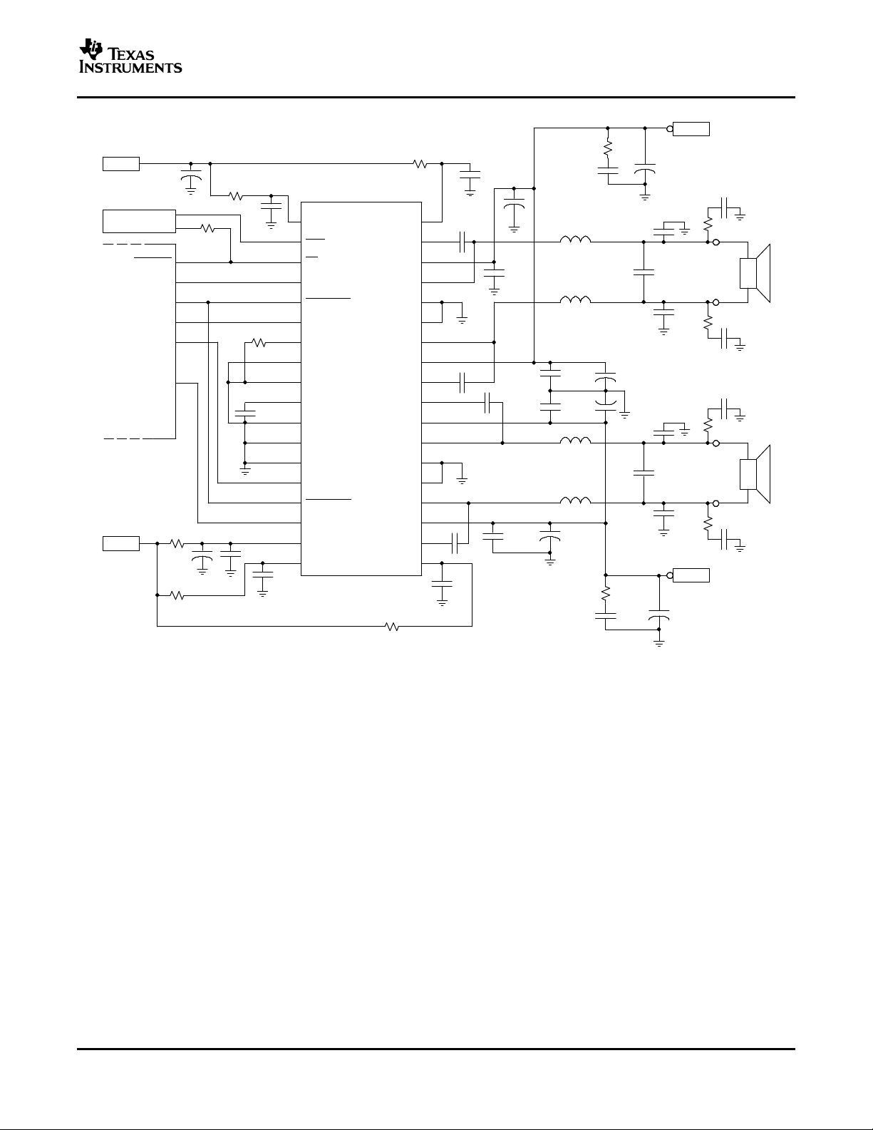
Figure 14. Typical Differential (2N) BTL Application With AD Modulation Filters
15
Page 16
www.ti.com
VALID
GVDD
10 Ω
10 Ω
10 µF
100 nF
GVDD
1 Ω
100 nF
Shutdown
PWM1
PWM2
PWM_A
PWM_C
OTW
RESET_AB
M2
M3
RESET_CD
VDD
GVDD_C
GVDD_B
PWM_D
VREG
M1
SD
AGND
PWM_B
OC_ADJ
GND
GND_C
OUT_A
BST_A
OUT_B
BST_B
PVDD_B
PVDD_A
BST_C
PVDD_C
OUT_C
GND_A
GND_B
OUT_D
PVDD_D
BST_D
36
35
34
33
23
19
20
21
22
24
25
26
27
28
32
31
30
29
GND_D
GVDD_D
GVDD_A
13
14
15
16
17
18
1
2
3
4
5
6
7
8
9
10
11
12
Microcontroller
22 kΩ
100 nF
33 nF
33 nF
33 nF
100 nF
50 V
100 nF
50 V
100 nF
50 V
1000 µF
50 V
PVDD
470 nF
100 V
10 µH@10 A
10 nF
50 V
10 nF
50 V
3.3 Ω
3.3 Ω
100 nF
50 V
50 nF
100 V
3.3 Ω
10 nF
50 V
10 nF
50 V
1000 µF
50 V
PVDD
3.3 Ω
100 nF
50 V
47 µF
50 V
47 µF
50 V
47 µF
50 V
10 µF
100 nF
100 nF
100 nF
10 µH@10 A
TAS5142DKD
0 Ω
Optional
TAS5508
10 Ω
10 Ω
47 µF
50 V
470 nF
100 V
10 µH@10 A
10 nF
50 V
10 nF
50 V
3.3 Ω
3.3 Ω
100 nF
50 V
100 nF
50 V
10 µH@10 A
33 nF
No connect
No connect
S0070-02
TAS5142
SLES126B – DECEMBER 2004 – REVISED MAY 2005
16
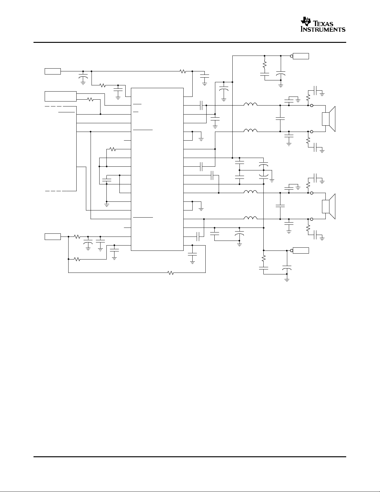
Figure 15. Typical Non-Differential (1N) BTL Application With AD Modulation Filters
Page 17
www.ti.com
PVDD/2
PVDD/2
PVDD/2
PVDD/2
VALID
GVDD
10 Ω
10 Ω
10 µF
100 nF
GVDD
1 Ω
100 nF
Shutdown
PWM1_P1
PWM2_P
PWM3_P
PWM4_P
PWM_A
PWM_C
OTW
RESET_AB
M2
M3
RESET_CD
VDD
GVDD_C
GVDD_B
PWM_D
VREG
M1
SD
AGND
PWM_B
OC_ADJ
GND
GND_C
OUT_A
BST_A
OUT_B
BST_B
PVDD_B
PVDD_A
BST_C
PVDD_C
OUT_C
GND_A
GND_B
OUT_D
PVDD_D
BST_D
36
35
34
33
23
19
20
21
22
24
25
26
27
28
32
31
30
29
GND_D
GVDD_D
GVDD_A
13
14
15
16
17
18
1
2
3
4
5
6
7
8
9
10
11
12
Microcontroller
39 kΩ
100 nF
33 nF
33 nF
33 nF
33 nF
100 nF
50 V
100 nF
50 V
100 nF
50 V
1000 µF
50 V
PVDD
10 µH@10 A
3.3 Ω
10 nF
50 V
10 nF
50 V
1000 µF
50 V
PVDD
3.3 Ω
100 nF
50 V
47 µF
50 V
47 µF
50 V
47 µF
50 V
10 µF
100 nF
100 nF
100 nF
10 µH@10 A
TAS5142DKD
0 Ω
Optional
TAS5508
10 Ω
10 Ω
47 µF
50 V
10 µH@10 A
10 µH@10 A
10 nF
50 V
3.3 Ω
100 nF
100 V
10 nF @ 50 V
3.3 Ω
100 nF
100 V
1 µF
50 V
A
B
C
D
220 µF
50 V
220 µF
50 V
PVDD
D
C
2.7 kΩ
10 nF
50 V
3.3 Ω
100 nF
100 V
10 nF @ 50 V
3.3 Ω
100 nF
100 V
1 µF
50 V
220 µF
50 V
220 µF
50 V
PVDD
10 nF
50 V
3.3 Ω
100 nF
100 V
10 nF @ 50 V
3.3 Ω
100 nF
100 V
1 µF
50 V
220 µF
50 V
220 µF
50 V
PVDD
10 nF
50 V
3.3 Ω
100 nF
100 V
10 nF @ 50 V
3.3 Ω
100 nF
100 V
1 µF
50 V
220 µF
50 V
220 µF
50 V
PVDD
2.7 kΩ
2.7 kΩ
2.7 kΩ
A
B
S0071-01
TAS5142
SLES126B – DECEMBER 2004 – REVISED MAY 2005
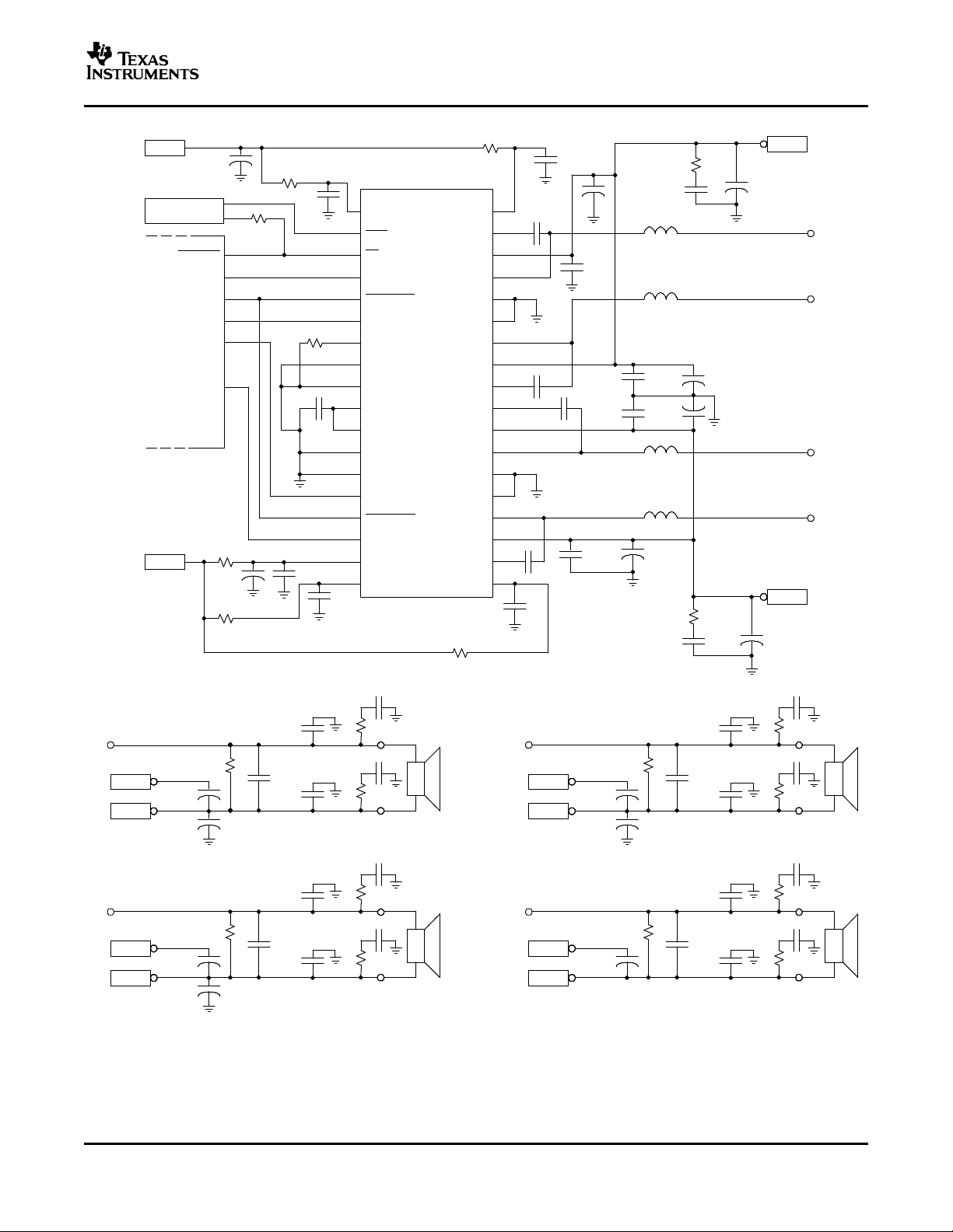
Figure 16. Typical SE Application
17
Page 18
www.ti.com
VALID
GVDD
10 Ω
10 Ω
10 µF
100 nF
GVDD
1 Ω
100 nF
Shutdown
PWM1_P PWM_A
PWM_C
OTW
RESET_AB
M2
M3
RESET_CD
VDD
GVDD_C
GVDD_B
PWM_D
VREG
M1
SD
AGND
PWM_B
OC_ADJ
GND
GND_C
OUT_A
BST_A
OUT_B
BST_B
PVDD_B
PVDD_A
BST_C
PVDD_C
OUT_C
GND_A
GND_B
OUT_D
PVDD_D
BST_D
36
35
34
33
23
19
20
21
22
24
25
26
27
28
32
31
30
29
GND_D
GVDD_D
GVDD_A
13
14
15
16
17
18
1
2
3
4
5
6
7
8
9
10
11
12
Microcontroller
30 kΩ
100 nF
33 nF
33 nF
33 nF
100 nF
50 V
100 nF
50 V
100 nF
50 V
1000 µF
50 V
PVDD
10 µH@10 A
3.3 Ω
10 nF
50 V
10 nF
50 V
1000 µF
50 V
PVDD
3.3 Ω
100 nF
50 V
47 µF
50 V
47 µF
50 V
47 µF
50 V
10 µF
100 nF
100 nF
100 nF
10 µH@10 A
TAS5142DKD
0 Ω
Optional
TAS5508
10 Ω
10 Ω
47 µF
50 V
10 µH@10 A
10 µH@10 A
33 nF
PWM1_M
470 nF
63 V
10 nF
50 V
10 nF
50 V
3.3 Ω
3.3 Ω
100 nF
100 V
100 nF
100 V
S0070-03
TAS5142
SLES126B – DECEMBER 2004 – REVISED MAY 2005
18
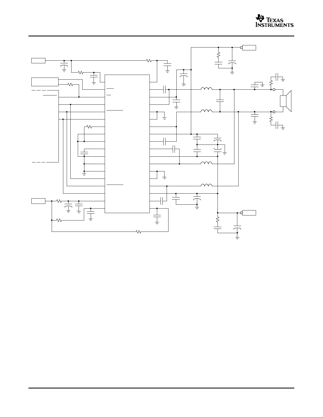
Figure 17. Typical Differential (2N) PBTL Application With AD Modulation Filters
Page 19

www.ti.com
VALID
GVDD
10 Ω
10 Ω
10 µF
100 nF
GVDD
1 Ω
100 nF
Shutdown
PWM1 PWM_A
PWM_C
OTW
RESET_AB
M2
M3
RESET_CD
VDD
GVDD_C
GVDD_B
PWM_D
VREG
M1
SD
AGND
PWM_B
OC_ADJ
GND
GND_C
OUT_A
BST_A
OUT_B
BST_B
PVDD_B
PVDD_A
BST_C
PVDD_C
OUT_C
GND_A
GND_B
OUT_D
PVDD_D
BST_D
36
35
34
33
23
19
20
21
22
24
25
26
27
28
32
31
30
29
GND_D
GVDD_D
GVDD_A
13
14
15
16
17
18
1
2
3
4
5
6
7
8
9
10
11
12
Microcontroller
30 kΩ
100 nF
33 nF
33 nF
33 nF
100 nF
50 V
100 nF
50 V
100 nF
50 V
1000 µF
50 V
PVDD
10 µH@10 A
3.3 Ω
10 nF
50 V
10 nF
50 V
1000 µF
50 V
PVDD
3.3 Ω
100 nF
50 V
47 µF
50 V
47 µF
50 V
47 µF
50 V
10 µF
100 nF
100 nF
100 nF
10 µH@10 A
TAS5142DKD
0 Ω
Optional
TAS5508
10 Ω
10 Ω
47 µF
50 V
10 µH@10 A
10 µH@10 A
33 nF
470 nF
63 V
10 nF
50 V
10 nF
50 V
3.3 Ω
3.3 Ω
100 nF
100 V
100 nF
100 V
No connect
No connect
No connect
S0070-04
TAS5142
SLES126B – DECEMBER 2004 – REVISED MAY 2005
Figure 18. Typical Non-Differential (1N) PBTL Application
19
Page 20

www.ti.com
TAS5142
SLES126B – DECEMBER 2004 – REVISED MAY 2005
THEORY OF OPERATION
POWER SUPPLIES
To facilitate system design, the TAS5142 needs only
a 12-V supply in addition to the (typical) 32-V
power-stage supply. An internal voltage regulator
provides suitable voltage levels for the digital and
low-voltage analog circuitry. Additionally, all circuitry
requiring a floating voltage supply, e.g., the high-side
gate drive, is accommodated by built-in bootstrap
circuitry requiring only a few external capacitors.
In order to provide outstanding electrical and acoustical characteristics, the PWM signal path including
gate drive and output stage is designed as identical,
independent half-bridges. For this reason, each
half-bridge has separate gate drive supply
(GVDD_X), bootstrap pins (BST_X), and power-stage
supply pins (PVDD_X). Furthermore, an additional pin
(VDD) is provided as supply for all common circuits.
Although supplied from the same 12-V source, it is
highly recommended to separate GVDD_A,
GVDD_B, GVDD_C, GVDD_D, and VDD on the
printed-circuit board (PCB) by RC filters (see application diagram for details). These RC filters provide
the recommended high-frequency isolation. Special
Special attention should be paid to the power-stage
power supply; this includes component selection,
PCB placement, and routing. As indicated, each
half-bridge has independent power-stage supply pins
(PVDD_X). For optimal electrical performance, EMI
compliance, and system reliability, it is important that
each PVDD_X pin is decoupled with a 100-nF ceramic capacitor placed as close as possible to each
supply pin. It is recommended to follow the PCB
layout of the TAS5142 reference design. For additional information on recommended power supply
and required components, see the application diagrams given previously in this data sheet.
The 12-V supply should be from a low-noise,
low-output-impedance voltage regulator. Likewise, the
32-V power-stage supply is assumed to have low
output impedance and low noise. The power-supply
sequence is not critical as facilitated by the internal
power-on-reset circuit. Moreover, the TAS5142 is fully
protected against erroneous power-stage turnon due
to parasitic gate charging. Thus, voltage-supply ramp
rates (dV/dt) are non-critical within the specified
range (see the Recommended Operating Conditions
section of this data sheet).
attention should be paid to placing all decoupling
capacitors as close to their associated pins as poss-
SYSTEM POWER-UP/POWER-DOWN
ible. In general, inductance between the power supply SEQUENCE
pins and decoupling capacitors must be avoided.
(See reference board documentation for additional
information.)
Powering Up
The TAS5142 does not require a power-up sequence.
For a properly functioning bootstrap circuit, a small The outputs of the H-bridges remain in a high-impedceramic capacitor must be connected from each ance state until the gate-drive supply voltage
bootstrap pin (BST_X) to the power-stage output pin (GVDD_X) and VDD voltage are above the
(OUT_X). When the power-stage output is low, the undervoltage protection (UVP) voltage threshold (see
bootstrap capacitor is charged through an internal the Electrical Characteristics section of this data
diode connected between the gate-drive power-- sheet). Although not specifically required, it is recsupply pin (GVDD_X) and the bootstrap pin. When ommended to hold RESET_AB and RESET_CD in a
the power-stage output is high, the bootstrap capaci- low state while powering up the device. This allows
tor potential is shifted above the output potential and an internal circuit to charge the external bootstrap
thus provides a suitable voltage supply for the capacitors by enabling a weak pulldown of the
high-side gate driver. In an application with PWM half-bridge output.
switching frequencies in the range from 352 kHz to
384 kHz, it is recommended to use 33-nF ceramic
capacitors, size 0603 or 0805, for the bootstrap
supply. These 33-nF capacitors ensure sufficient
energy storage, even during minimal PWM duty
cycles, to keep the high-side power stage FET
When the TAS5142 is being used with TI PWM
modulators such as the TAS5508, no special atten-
tion to the state of RESET_AB and RESET_CD is
required, provided that the chipset is configured as
recommended.
(LDMOS) fully turned on during the remaining part of
the PWM cycle. In an application running at a
reduced switching frequency, generally 192 kHz, the
bootstrap capacitor might need to be increased in
value.
20
Page 21
www.ti.com
TAS5142
SLES126B – DECEMBER 2004 – REVISED MAY 2005
Powering Down
The TAS5142 does not require a power-down sequence. The device remains fully operational as long
as the gate-drive supply (GVDD_X) voltage and VDD
voltage are above the undervoltage protection (UVP)
voltage threshold (see the Electrical Characteristics
section of this data sheet). Although not specifically
required, it is a good practice to hold RESET_AB and
RESET_CD low during power down, thus preventing
audible artifacts including pops or clicks.
When the TAS5142 is being used with TI PWM
modulators such as the TAS5508, no special attention to the state of RESET_AB and RESET_CD is
required, provided that the chipset is configured as
recommended.
ERROR REPORTING
The SD and OTW pins are both active-low,
open-drain outputs. Their function is for protection-mode signaling to a PWM controller or other
system-control device.
Any fault resulting in device shutdown is signaled by
the SD pin going low. Likewise, OTW goes low when
the device junction temperature exceeds 125 ° C (see
the following table).
SD OTW DESCRIPTION
0 0 Overtemperature (OTE) or overload (OLP) or
undervoltage (UVP)
0 1 Overload (OLP) or undervoltage (UVP)
1 0 Junction temperature higher than 125°C
(overtemperature warning)
1 1 Junction temperature lower than 125°C and no
OLP or UVP faults (normal operation)
Note that asserting either RESET_AB or RESET_CD
low forces the SD signal high, independent of faults
being present. TI recommends monitoring the OTW
signal using the system microcontroller and responding to an overtemperature warning signal by,
e.g., turning down the volume to prevent further
heating of the device resulting in device shutdown
(OTE).
To reduce external component count, an internal
pullup resistor to 3.3 V is provided on both SD and
OTW outputs. Level compliance for 5-V logic can be
obtained by adding external pullup resistors to 5 V
(see the Electrical Characteristics section of this data
sheet for further specifications).
DEVICE PROTECTION SYSTEM
The TAS5142 contains advanced protection circuitry
carefully designed to facilitate system integration and
ease of use, as well as to safeguard the device from
permanent failure due to a wide range of fault
conditions such as short circuits, overload,
overtemperature, and undervoltage. The TAS5142
responds to a fault by immediately setting the power
stage in a high-impedance (Hi-Z) state and asserting
the SD pin low. In situations other than overload, the
device automatically recovers when the fault condition has been removed, i.e., the junction temperature has dropped or the supply voltage has increased. For highest possible reliability, recovering
from an overload fault requires external reset of the
device (see the Device Reset section of this data
sheet) no sooner than 1 second after the shutdown.
Use of TAS5142 in High-Modulation-Index
Capable Systems
This device requires at least 50 ns of low time on the
output per 384-kHz PWM frame rate in order to keep
the bootstrap capacitors charged. As an example, if
the modulation index is set to 99.2% in the TAS5508,
this setting allows PWM pulse durations down to 20
ns. This signal, which does not meet the 50-ns
requirement, is sent to the PWM_X pin and this
low-state pulse time does not allow the bootstrap
capacitor to stay charged. In this situation, the low
voltage across the bootstrap capacitor can cause a
failure of the high-side MOSFET transistor, especially
when driving a low-impedance load. The TAS5142
device requires limiting the TAS5508 modulation
index to 96.1% to keep the bootstrap capacitor
charged under all signals and loads.
Therefore, TI strongly recommends using a TI PWM
processor, such as TAS5508 or TAS5086, with the
modulation index set at 96.1% to interface with
TAS5142.
Overcurrent (OC) Protection With Current
Limiting and Overload Detection
The device has independent, fast-reacting current
detectors with programmable trip threshold (OC
threshold) on all high-side and low-side power-stage
FETs. See the following table for OC-adjust resistor
values. The detector outputs are closely monitored by
two protection systems. The first protection system
controls the power stage in order to prevent the
output current from further increasing, i.e., it performs
a current-limiting function rather than prematurely
shutting down during combinations of high-level music transients and extreme speaker load impedance
drops. If the high-current situation persists, i.e., the
power stage is being overloaded, a second protection
system triggers a latching shutdown, resulting in the
power stage being set in the high-impedance (Hi-Z)
state. Current limiting and overload protection are
independent for half-bridges A and B and, respectively, C and D. That is, if the bridge-tied load between
half-bridges A and B causes an overload fault, only
half-bridges A and B are shut down.
21
Page 22

www.ti.com
TAS5142
SLES126B – DECEMBER 2004 – REVISED MAY 2005
• For the lowest-cost bill of materials in terms of ( OTW) when the device junction temperature ex-
component selection, the OC threshold measure ceeds 125 ° C (nominal) and, if the device junction
should be limited, considering the power output temperature exceeds 155 ° C (nominal), the device is
requirement and minimum load impedance. put into thermal shutdown, resulting in all half-bridge
Higher-impedance loads require a lower OC outputs being set in the high-impedance (Hi-Z) state
threshold. and SD being asserted low. OTE is latched in this
• The demodulation-filter inductor must retain at
least 5 µ H of inductance at twice the OC
threshold setting.
Unfortunately, most inductors have decreasing inductance with increasing temperature and increasing
current (saturation). To some degree, an increase in
temperature naturally occurs when operating at high
output currents, due to core losses and the dc
resistance of the inductor's copper winding. A
thorough analysis of inductor saturation and thermal
properties is strongly recommended.
Setting the OC threshold too low might cause issues
such as lack of enough output power and/or unexpected shutdowns due to too-sensitive overload detection.
In general, it is recommended to follow closely the
external component selection and PCB layout as
given in the Application section.
For added flexibility, the OC threshold is
programmable within a limited range using a single
external resistor connected between the OC_ADJ pin
and AGND. (See the Electrical Characteristics section
of this data sheet for information on the correlation
between programming-resistor value and the OC
threshold.) It should be noted that a properly functioning overcurrent detector assumes the presence of
a properly designed demodulation filter at the
power-stage output. Short-circuit protection is not
provided directly at the output pins of the power stage
but only on the speaker terminals (after the demodulation filter). It is required to follow certain guidelines
when selecting the OC threshold and an appropriate
demodulation inductor:
OC-Adjust Resistor Values Max. Current Before OC Occurs
(k Ω ) (A) and it is therefore recommended to ensure bootstrap
22 9.4
27 8.6
39 6.4
47 6
69 4.7
Overtemperature Protection
The TAS5142 has a two-level temperature-protection
system that asserts an active-low warning signal
case. To clear the OTE latch, both RESET_AB and
RESET_CD must be asserted. Thereafter, the device
resumes normal operation.
Undervoltage Protection (UVP) and Power-On
Reset (POR)
The UVP and POR circuits of the TAS5142 fully
protect the device in any power-up/down and
brownout situation. While powering up, the POR
circuit resets the overload circuit (OLP) and ensures
that all circuits are fully operational when the
GVDD_X and VDD supply voltages reach 9.8 V
(typical). Although GVDD_X and VDD are independently monitored, a supply voltage drop below the
UVP threshold on any VDD or GVDD_X pin results in
all half-bridge outputs immediately being set in the
high-impedance (Hi-Z) state and SD being asserted
low. The device automatically resumes operation
when all supply voltages have increased above the
UVP threshold.
DEVICE RESET
Two reset pins are provided for independent control
of half-bridges A/B and C/D. When RESET_AB is
asserted low, all four power-stage FETs in half--
bridges A and B are forced into a high-impedance
(Hi-Z) state. Likewise, asserting RESET_CD low
forces all four power-stage FETs in half-bridges C
and D into a high-impedance state. Thus, both reset
pins are well suited for hard-muting the power stage if
needed.
In BTL modes, to accommodate bootstrap charging
prior to switching start, asserting the reset inputs low
enables weak pulldown of the half-bridge outputs. In
the SE mode, the weak pulldowns are not enabled,
capacitor charging by providing a low pulse on the
PWM inputs when reset is asserted high.
Asserting either reset input low removes any fault
information to be signalled on the SD output, i.e., SD
is forced high.
A rising-edge transition on either reset input allows
the device to resume operation after an overload
fault.
22
Page 23

Page 24

Page 25

PACKAGE OPTION ADDENDUM
www.ti.com
16-May-2005
PACKAGING INFORMATION
Orderable Device Status
(1)
Package
Type
Package
Drawing
Pins Package
Qty
Eco Plan
TAS5142DDV ACTIVE HTSSOP DDV 44 35 Green (RoHS &
no Sb/Br)
TAS5142DDVG4 ACTIVE HTSSOP DDV 44 35 Green (RoHS &
no Sb/Br)
TAS5142DDVR ACTIVE HTSSOP DDV 44 2000 Green (RoHS &
no Sb/Br)
TAS5142DDVRG4 ACTIVE HTSSOP DDV 44 2000 Green (RoHS &
no Sb/Br)
TAS5142DKD ACTIVE SSOP DKD 36 29 Pb-Free
TAS5142DKDR ACTIVE SSOP DKD 36 500 Pb-Free
(1)
The marketing status values are defined as follows:
ACTIVE: Product device recommended for new designs.
LIFEBUY: TI has announced that the device willbe discontinued, and a lifetime-buy period is in effect.
NRND: Not recommended for new designs. Device is in production to support existing customers, but TI does not recommend using this part in
a new design.
PREVIEW: Device has been announced but is not in production. Samples may or may not be available.
OBSOLETE: TI has discontinued the production of the device.
(RoHS)
(RoHS)
(2)
Lead/Ball Finish MSL Peak Temp
CU NIPDAU Level-3-260C-168 HR
CU NIPDAU Level-3-260C-168 HR
CU NIPDAU Level-3-260C-168 HR
CU NIPDAU Level-3-260C-168 HR
CU SNBI Level-4-260C-72 HR/
Level-2-220C-1 YEAR
CU SNBI Level-4-260C-72 HR/
Level-2-220C-1 YEAR
(3)
(2)
Eco Plan - The planned eco-friendly classification: Pb-Free (RoHS) or Green (RoHS & no Sb/Br) - please check
http://www.ti.com/productcontent for the latest availability information and additional product content details.
TBD: The Pb-Free/Green conversion plan has not been defined.
Pb-Free (RoHS): TI's terms "Lead-Free" or "Pb-Free" mean semiconductor products that are compatible with the current RoHS requirements
for all 6 substances, including the requirement that lead not exceed 0.1% by weight in homogeneous materials. Where designed to be soldered
at high temperatures, TI Pb-Free products are suitable for use in specified lead-free processes.
Green (RoHS & no Sb/Br): TI defines "Green" to mean Pb-Free (RoHS compatible), and free of Bromine (Br) and Antimony (Sb) based flame
retardants (Br or Sb do not exceed 0.1% by weight in homogeneous material)
(3)
MSL, Peak Temp. -- The Moisture Sensitivity Level rating according to the JEDEC industry standard classifications, and peak solder
temperature.
Important Information and Disclaimer:The information provided on this page represents TI's knowledge and belief as of the date that it is
provided. TI bases its knowledge and belief on information provided by third parties, and makes no representation or warranty as to the
accuracy of such information. Efforts are underway to better integrate information from third parties. TI has taken and continues to take
reasonable steps to provide representative and accurate information but may not have conducted destructive testing or chemical analysis on
incoming materials and chemicals. TI and TI suppliers consider certain information to be proprietary, and thus CAS numbers and other limited
information may not be available for release.
In no event shall TI's liability arising out of such information exceed the total purchase price of the TI part(s) at issue in this document sold by TI
to Customer on an annual basis.
Addendum-Page 1
Page 26

IMPORTANT NOTICE
Texas Instruments Incorporated and its subsidiaries (TI) reserve the right to make corrections, modifications,
enhancements, improvements, and other changes to its products and services at any time and to discontinue
any product or service without notice. Customers should obtain the latest relevant information before placing
orders and should verify that such information is current and complete. All products are sold subject to TI’s terms
and conditions of sale supplied at the time of order acknowledgment.
TI warrants performance of its hardware products to the specifications applicable at the time of sale in
accordance with TI’s standard warranty. Testing and other quality control techniques are used to the extent TI
deems necessary to support this warranty . Except where mandated by government requirements, testing of all
parameters of each product is not necessarily performed.
TI assumes no liability for applications assistance or customer product design. Customers are responsible for
their products and applications using TI components. To minimize the risks associated with customer products
and applications, customers should provide adequate design and operating safeguards.
TI does not warrant or represent that any license, either express or implied, is granted under any TI patent right,
copyright, mask work right, or other TI intellectual property right relating to any combination, machine, or process
in which TI products or services are used. Information published by TI regarding third-party products or services
does not constitute a license from TI to use such products or services or a warranty or endorsement thereof.
Use of such information may require a license from a third party under the patents or other intellectual property
of the third party, or a license from TI under the patents or other intellectual property of TI.
Reproduction of information in TI data books or data sheets is permissible only if reproduction is without
alteration and is accompanied by all associated warranties, conditions, limitations, and notices. Reproduction
of this information with alteration is an unfair and deceptive business practice. TI is not responsible or liable for
such altered documentation.
Resale of TI products or services with statements different from or beyond the parameters stated by TI for that
product or service voids all express and any implied warranties for the associated TI product or service and
is an unfair and deceptive business practice. TI is not responsible or liable for any such statements.
Following are URLs where you can obtain information on other Texas Instruments products and application
solutions:
Products Applications
Amplifiers amplifier.ti.com Audio www.ti.com/audio
Data Converters dataconverter.ti.com Automotive www.ti.com/automotive
DSP dsp.ti.com Broadband www.ti.com/broadband
Interface interface.ti.com Digital Control www.ti.com/digitalcontrol
Logic logic.ti.com Military www.ti.com/military
Power Mgmt power.ti.com Optical Networking www.ti.com/opticalnetwork
Microcontrollers microcontroller.ti.com Security www.ti.com/security
Telephony www.ti.com/telephony
Video & Imaging www.ti.com/video
Wireless www.ti.com/wireless
Mailing Address: Texas Instruments
Post Office Box 655303 Dallas, Texas 75265
Copyright 2005, Texas Instruments Incorporated
 Loading...