How it Works
Log In / Sign Up
Buy Points
How it Works
FAQ
Contact Us
Questions and Suggestions
Users
TEXAS INSTRUMENTS
Loading...
S
System-Side Impedance Track bq27500
T
TA5704EVM
TAFE1040CPFB
Tag-it RI-K01-320A
Tag-it RI-K02-320A
TAP6203A1
TAS1020A
TAS1020APFB
TAS1020B
3
TAS1020BEVM
TAS1020BPFB
TAS2505
TAS2559
TAS2770
2
TAS3001C
3
TAS3001CPW
TAS3002
3
TAS3004
TAS3103
TAS3108EVM2
TAS3204
TAS3204PAG
TAS3208
TAS3208EVM
TAS3208PZP
TAS3251
TAS5000
TAS5001
TAS5010
TAS5010−5112F2EVM
TAS5012
TAS5015
TAS5026
TAS5026A
TAS5026REF
TAS5036
TAS5066-5111D6EVM PurePath Digital
TAS5066PAG
TAS5076
2
TAS5086
2
TAS5100A
TAS5101
TAS5102
2
TAS5102EVM
TAS5103
2
TAS5103EVM
2
TAS5110
TAS5110A
TAS5110D6REF
TAS5111
2
TAS5112
2
TAS5112A
TAS5121
2
TAS5122
TAS5142
3
TAS5142DKDRG4
TAS5152
2
TAS5152DKDRG4
TAS5152K8EVM
TAS5162
TAS5162DKDRG4
TAS5182
TAS5186
2
TAS5186A
2
TAS5261
TAS5261DKDRG4
TAS5342
tas5352a
TAS5414CEVM
TAS5508
TAS5508-5121K8EVM
2
TAS5508-5142K7EVM
TAS5508C
TAS5518
TAS5518-5152K8EVM
TAS5518EVM
TAS5601
TAS 5611-13PHD2EVM
TAS5611PHD2EVM
TAS5613PHD2EVM
TAS5706EVM2
TAS5707
TAS5707A
TAS5711
TAS5713
TAS5727
TAS5733L
TAS5733LEVM
TAS5782M
2
TAS6424L-Q1
TB5R3
TBP24S10J
TBP24S10MJ
TBP24S10N
TBP24S41J
TBP24S41MJ
TBP24S41N
TBP24S81J
TBP24S81MJ
TBP24S81N
Loading...
Loading...
Nothing found
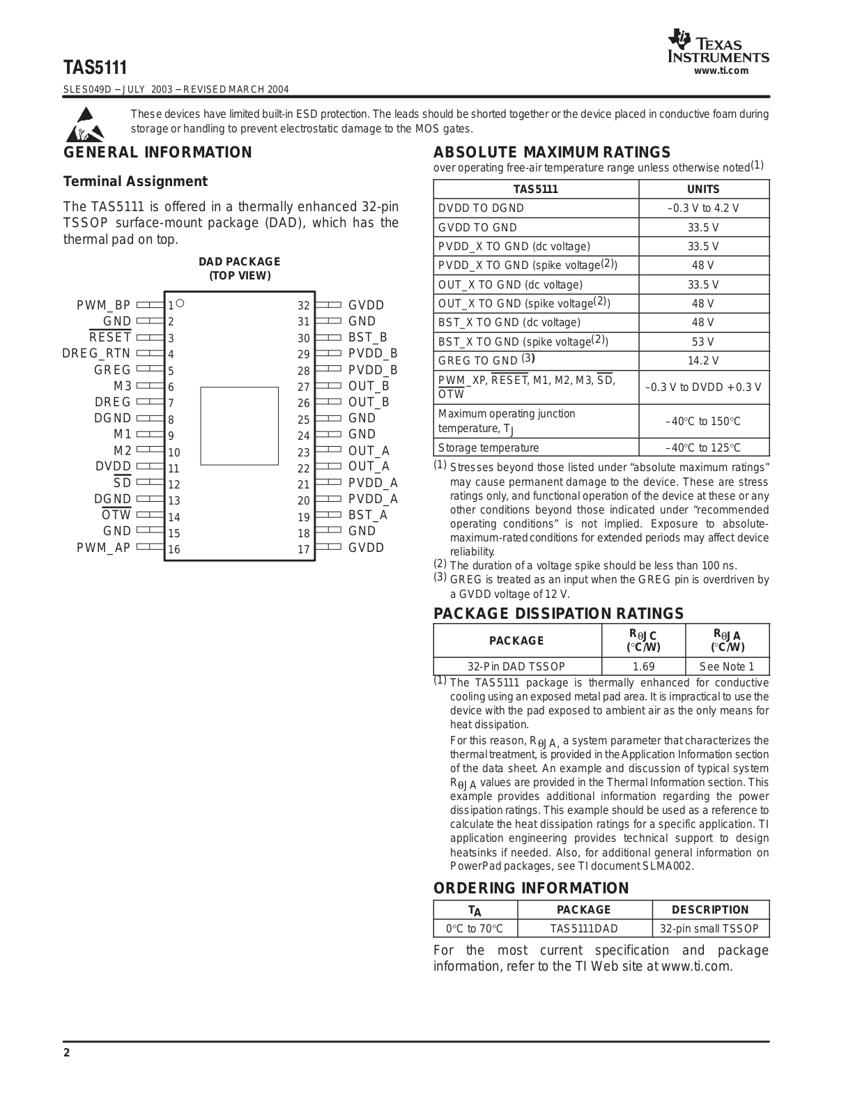
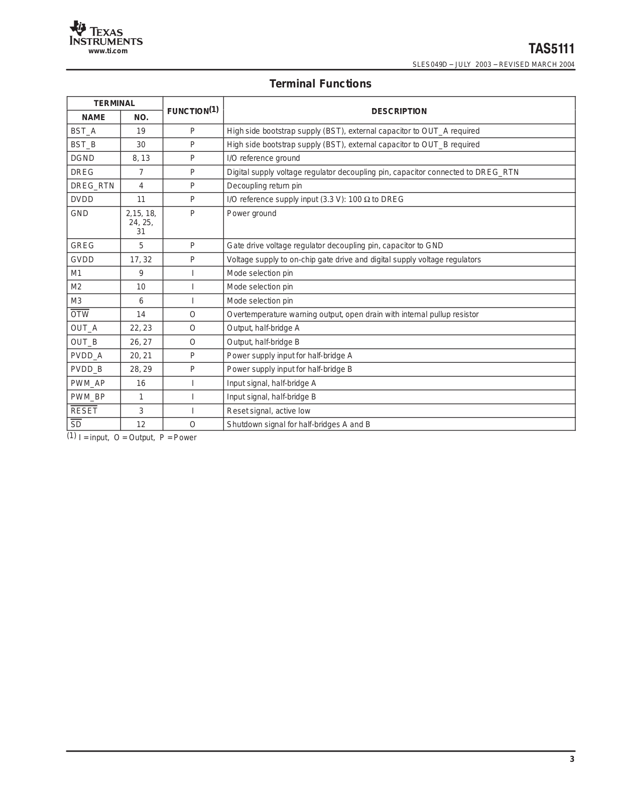
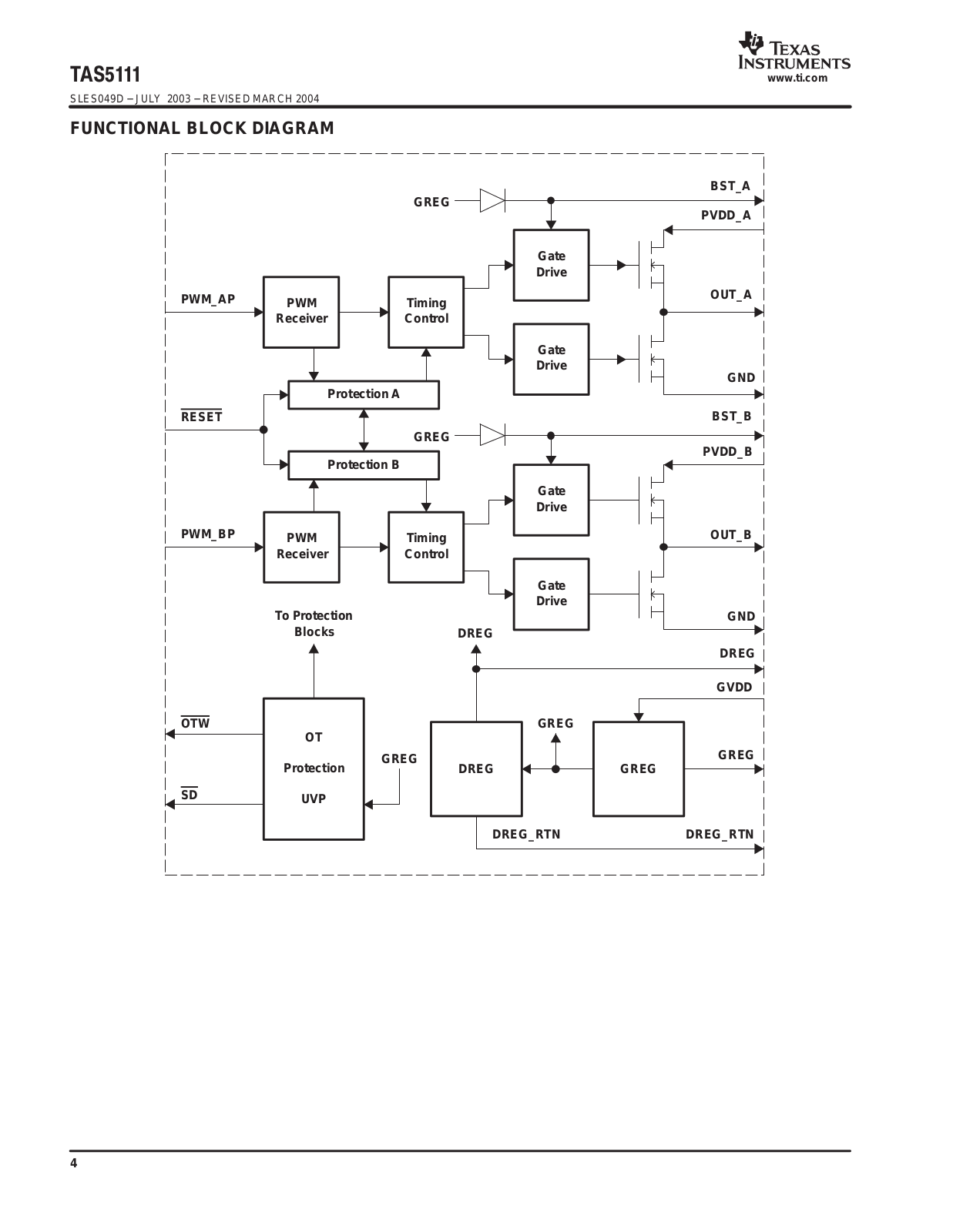
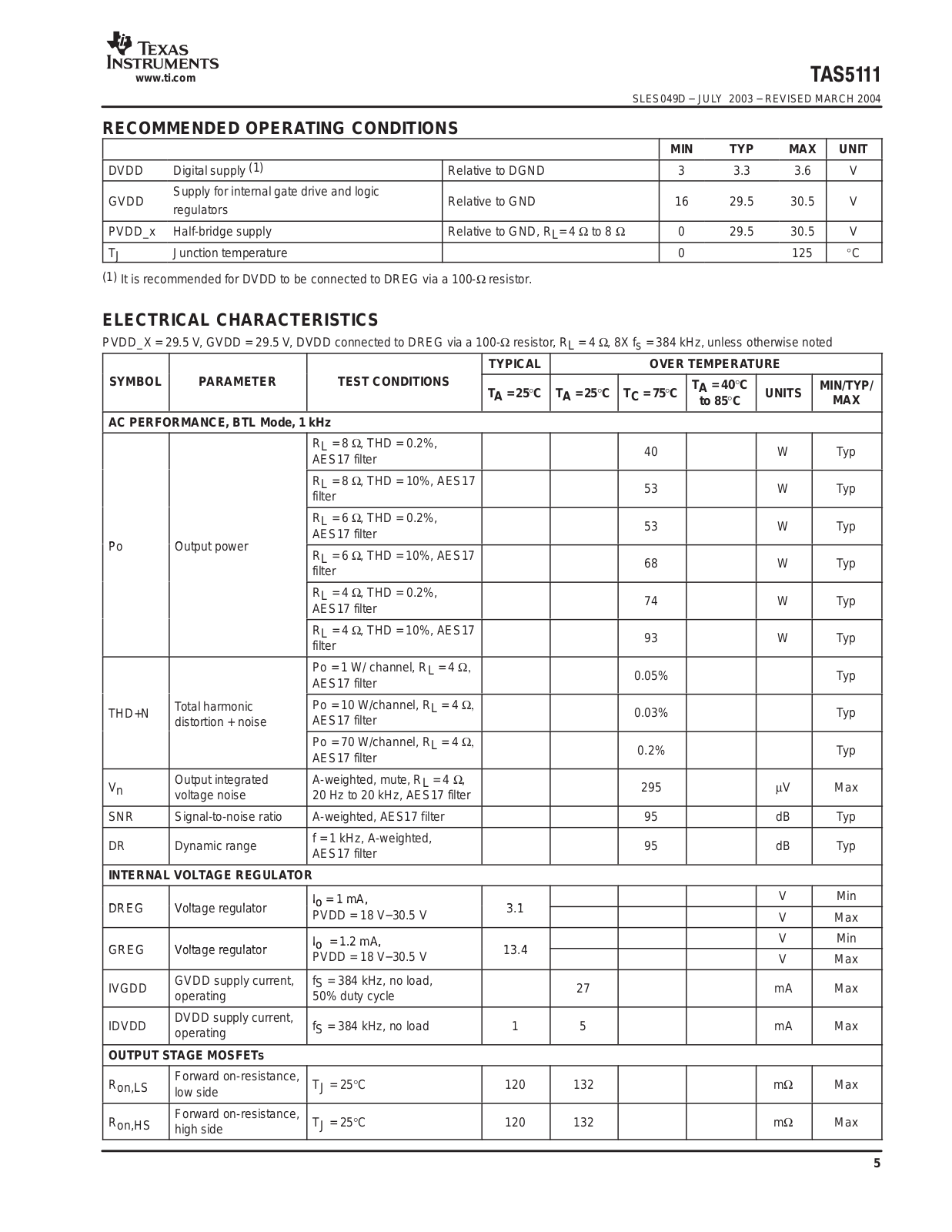
TAS5111
Technical data
16 pgs
200.4 Kb
0
User Manual
42 pgs
898.99 Kb
0
Table of contents
Loading...
TEXAS INSTRUMENTS TAS5111 Technical data
...
TEXAS INSTRUMENTS Technical data
Download
Specifications and Main Features
Frequently Asked Questions
User Manual
Download
Loading...
+
hidden pages
Unhide
You need points to download manuals.
1 point = 1 manual.
You can buy points or you can get point for every manual you upload.
Buy points
Upload your manuals