

Page 1

TAS5110D6REF
Reference Design for the TAS5110DAD Digital
Audio PWM Power Output Stage
User’s Guide
July 2003 Digital Audio/Application
SLEU032
Page 2

IMPORTANT NOTICE
Texas Instruments Incorporated and its subsidiaries (TI) reserve the right to make corrections, modifications,
enhancements, improvements, and other changes to its products and services at any time and to discontinue
any product or service without notice. Customers should obtain the latest relevant information before placing
orders and should verify that such information is current and complete. All products are sold subject to TI’s terms
and conditions of sale supplied at the time of order acknowledgment.
TI warrants performance of its hardware products to the specifications applicable at the time of sale in
accordance with TI’s standard warranty . Testing and other quality control techniques are used to the extent TI
deems necessary to support this warranty . Except where mandated by government requirements, testing of all
parameters of each product is not necessarily performed.
TI assumes no liability for applications assistance or customer product design. Customers are responsible for
their products and applications using TI components. T o minimize the risks associated with customer products
and applications, customers should provide adequate design and operating safeguards.
TI does not warrant or represent that any license, either express or implied, is granted under any TI patent right,
copyright, mask work right, or other TI intellectual property right relating to any combination, machine, or process
in which TI products or services are used. Information published by TI regarding third-party products or services
does not constitute a license from TI to use such products or services or a warranty or endorsement thereof.
Use of such information may require a license from a third party under the patents or other intellectual property
of the third party , or a license from TI under the patents or other intellectual property of TI.
Reproduction of information in TI data books or data sheets is permissible only if reproduction is without
alteration and is accompanied by all associated warranties, conditions, limitations, and notices. Reproduction
of this information with alteration is an unfair and deceptive business practice. TI is not responsible or liable for
such altered documentation.
Resale of TI products or services with statements different from or beyond the parameters stated by TI for that
product or service voids all express and any implied warranties for the associated TI product or service and
is an unfair and deceptive business practice. TI is not responsible or liable for any such statements.
Following are URLs where you can obtain information on other Texas Instruments products and application
solutions:
Products Applications
Amplifiers amplifier.ti.com Audio www.ti.com/audio
Data Converters dataconverter.ti.com Automotive www.ti.com/automotive
DSP dsp.ti.com Broadband www.ti.com/broadband
Interface interface.ti.com Digital Control www.ti.com/digitalcontrol
Logic logic.ti.com Military www.ti.com/military
Power Mgmt power.ti.com Optical Networking www.ti.com/opticalnetwork
Microcontrollers microcontroller.ti.com Security www.ti.com/security
Telephony www.ti.com/telephony
Video & Imaging www.ti.com/video
Wireless www.ti.com/wireless
Mailing Address: Texas Instruments
Post Office Box 655303 Dallas, Texas 75265
Copyright 2003, Texas Instruments Incorporated
Page 3

EVM IMPORTANT NOTICE
Texas Instruments (TI) provides the enclosed product(s) under the following conditions:
This evaluation kit being sold by TI is intended for use for ENGINEERING DEVELOPMENT OR EV ALUA TION
PURPOSES ONL Y and is not considered by TI to be fit for commercial use. As such, the goods being provided
may not be complete in terms of required design-, marketing-, and/or manufacturing-related protective
considerations, including product safety measures typically found in the end product incorporating the goods.
As a prototype, this product does not fall within the scope of the European Union directive on electromagnetic
compatibility and therefore may not meet the technical requirements of the directive.
Should this evaluation kit not meet the specifications indicated in the EVM User’s Guide, the kit may be returned
within 30 days from the date of delivery for a full refund. THE FOREGOING WARRANTY IS THE EXCLUSIVE
WARRANTY MADE BY SELLER TO BUYER AND IS IN LIEU OF ALL OTHER WARRANTIES, EXPRESSED,
IMPLIED, OR ST ATUT ORY, INCLUDING ANY W ARRANTY OF MERCHANTABILITY OR FITNESS FOR ANY
PARTICULAR PURPOSE.
The user assumes all responsibility and liability for proper and safe handling of the goods. Further, the user
indemnifies TI from all claims arising from the handling or use of the goods. Please be aware that the products
received may not be regulatory compliant or agency certified (FCC, UL, CE, etc.). Due to the open construction
of the product, it is the user’s responsibility to take any and all appropriate precautions with regard to electrostatic
discharge.
EXCEPT TO THE EXTENT OF THE INDEMNITY SET FORTH ABOVE, NEITHER P ARTY SHALL BE LIABLE
TO THE OTHER FOR ANY INDIRECT, SPECIAL, INCIDENTAL, OR CONSEQUENTIAL DAMAGES.
TI currently deals with a variety of customers for products, and therefore our arrangement with the user is not
exclusive.
TI assumes no liability for applications assistance, customer product design, software performance, or
infringement of patents or services described herein.
Please read the EVM User’s Guide and, specifically, the EVM Warnings and Restrictions notice in the EVM
User’s Guide prior to handling the product. This notice contains important safety information about temperatures
and voltages. For further safety concerns, please contact the TI application engineer.
Persons handling the product must have electronics training and observe good laboratory practice standards.
No license is granted under any patent right or other intellectual property right of TI covering or relating to any
machine, process, or combination in which such TI products or services might be or are used.
Mailing Address:
Texas Instruments
Post Office Box 655303
Dallas, Texas 75265
Copyright 2003, Texas Instruments Incorporated
Page 4

EVM WARNINGS AND RESTRICTIONS
It is important to operate this EVM within the specified input and output ranges described in
the EVM User’s Guide.
Exceeding the specified input range may cause unexpected operation and/or irreversible
damage to the EVM. If there are questions concerning the input range, please contact a TI
field representative prior to connecting the input power.
Applying loads outside of the specified output range may result in unintended operation and/or
possible permanent damage to the EVM. Please consult the EVM User’s Guide prior to
connecting any load to the EVM output. If there is uncertainty as to the load specification,
please contact a TI field representative.
During normal operation, some circuit components may have case temperatures greater than
60°C. The EVM is designed to operate properly with certain components above 60°C as long
as the input and output ranges are maintained. These components include but are not limited
to linear regulators, switching transistors, pass transistors, and current sense resistors. These
types of devices can be identified using the EVM schematic located in the EVM User’s Guide.
When placing measurement probes near these devices during operation, please be aware
that these devices may be very warm to the touch.
Mailing Address:
Texas Instruments
Post Office Box 655303
Dallas, Texas 75265
Copyright 2003, Texas Instruments Incorporated
Page 5

About This Manual
This manual describes the operation of the TAS5110D6REF evaluation
module from Texas Instruments.
How to Use This Manual
Information About Cautions and Warnings
Preface
Read This First
This document contains the following chapters:
- Chapter 1 – Introduction
- Chapter 2 – System Interfaces
- Chapter 3 – Electrical Specifications and Typical Characteristics Graphs
- Chapter 4 – Schematic, Parts List, PCB Specification, and PCB Layout
Information About Cautions and Warnings
This book may contain cautions and warnings.
This is an example of a caution statement.
A caution statement describes a situation that could potentially
damage your software or equipment.
This is an example of a warning statement.
A warning statement describes a situation that could potentially
cause harm to you
.
The information in a caution or a warning is provided for your protection.
Please read each caution and warning carefully.
iii
Page 6

Related Documentation From Texas Instruments
Related Documentation From Texas Instruments
The following is a list of data manual that have detailed descriptions of the
integrated circuits used in the design of the TAS5110D6REF evaluation
module. The data manuals can be obtained at the URL http://www.ti.com
Part Number Literature Number
TAS5110A
SN74LVC2G126DCT
TPS75333QPWP
.
SLES079
SCES205
SLVS241
iv
Page 7

Contents
Contents
1 Introduction 1-1. . . . . . . . . . . . . . . . . . . . . . . . . . . . . . . . . . . . . . . . . . . . . . . . . . . . . . . . . . . . . . . . . . . . .
1.1 TAS5110D6REF Features 1-2. . . . . . . . . . . . . . . . . . . . . . . . . . . . . . . . . . . . . . . . . . . . . . . . . . .
1.2 PCB Key Map 1-3. . . . . . . . . . . . . . . . . . . . . . . . . . . . . . . . . . . . . . . . . . . . . . . . . . . . . . . . . . . . . .
1.3 Short-Circuit Protection and Fault Reporting Circuitry 1-4. . . . . . . . . . . . . . . . . . . . . . . . . . . .
1.3.1 Device Fault Reporting 1-4. . . . . . . . . . . . . . . . . . . . . . . . . . . . . . . . . . . . . . . . . . . . . . .
1.3.2 Short-Circuit Protection 1-4. . . . . . . . . . . . . . . . . . . . . . . . . . . . . . . . . . . . . . . . . . . . . . .
1.3.3 Autorecovery System 1-4. . . . . . . . . . . . . . . . . . . . . . . . . . . . . . . . . . . . . . . . . . . . . . . .
2 System Interfaces 2-1. . . . . . . . . . . . . . . . . . . . . . . . . . . . . . . . . . . . . . . . . . . . . . . . . . . . . . . . . . . . . . .
2.1 PSU Interface (J150) 2-2. . . . . . . . . . . . . . . . . . . . . . . . . . . . . . . . . . . . . . . . . . . . . . . . . . . . . . . .
2.2 PSU Control Interface (J160) 2-3. . . . . . . . . . . . . . . . . . . . . . . . . . . . . . . . . . . . . . . . . . . . . . . . .
2.3 Loudspeaker Connectors (J240, J280, J340, J380, J440, and J480) 2-3. . . . . . . . . . . . . . .
2.4 PWM Interface (J100) 2-4. . . . . . . . . . . . . . . . . . . . . . . . . . . . . . . . . . . . . . . . . . . . . . . . . . . . . . .
3 Electrical Specifications and Typical Characteristics Graphs 3-1. . . . . . . . . . . . . . . . . . . . . . .
3.1 T AS5110D6REF Electrical Specifications 3-2. . . . . . . . . . . . . . . . . . . . . . . . . . . . . . . . . . . . . .
3.2 Physical Specifications 3-2. . . . . . . . . . . . . . . . . . . . . . . . . . . . . . . . . . . . . . . . . . . . . . . . . . . . . .
3.3 Typical Characteristics Graphs 3-3. . . . . . . . . . . . . . . . . . . . . . . . . . . . . . . . . . . . . . . . . . . . . . .
4 Schematic, Parts List, PCB Specification, and PCB Layout 4-1. . . . . . . . . . . . . . . . . . . . . . . . .
v
Page 8

Contents
Figures
1–1 TDAA System With TAS5026REF/TAS5036 and TAS5110D6REF Modules 1-2. . . . . . . . . . .
1–2 Physical Structure for the TAS5110D6REF (Rough Outline) 1-3. . . . . . . . . . . . . . . . . . . . . . . . .
1–3 Auto Recovery Loop 1-5. . . . . . . . . . . . . . . . . . . . . . . . . . . . . . . . . . . . . . . . . . . . . . . . . . . . . . . . . . .
2–1 Recommended T AS5110 Power-Up Sequence 2-2. . . . . . . . . . . . . . . . . . . . . . . . . . . . . . . . . . . .
2–2 Pin Numbers at the PSU Interface (Top View) 2-2. . . . . . . . . . . . . . . . . . . . . . . . . . . . . . . . . . . . .
2–3 Pin Numbers at the PSU Control Interface 2-3. . . . . . . . . . . . . . . . . . . . . . . . . . . . . . . . . . . . . . . .
2–4 Pin Numbers at the Loudspeaker Connectors 2-3. . . . . . . . . . . . . . . . . . . . . . . . . . . . . . . . . . . . .
2–5 Pin Numbers at PWM Interface (J100) 2-4. . . . . . . . . . . . . . . . . . . . . . . . . . . . . . . . . . . . . . . . . . .
3–1 THD+N vs Frequency – Channel 1 3-3. . . . . . . . . . . . . . . . . . . . . . . . . . . . . . . . . . . . . . . . . . . . . .
3–2 THD+N vs Power – Channel 1, 3, and 5 3-3. . . . . . . . . . . . . . . . . . . . . . . . . . . . . . . . . . . . . . . . . .
3–3 THD+N vs Power – Channel 2, 4, and 6 3-4. . . . . . . . . . . . . . . . . . . . . . . . . . . . . . . . . . . . . . . . . .
3–4 FFT With –60 dB Input Signal – Channel 1 3-4. . . . . . . . . . . . . . . . . . . . . . . . . . . . . . . . . . . . . . .
3–5 FFT at 40-W Output Power – Channel 1 3-5. . . . . . . . . . . . . . . . . . . . . . . . . . . . . . . . . . . . . . . . .
3–6 Noise Floor – Channel 1 3-5. . . . . . . . . . . . . . . . . . . . . . . . . . . . . . . . . . . . . . . . . . . . . . . . . . . . . . .
3–7 Channel Separation vs Frequency – Channel 1 3-6. . . . . . . . . . . . . . . . . . . . . . . . . . . . . . . . . . .
3–8 Frequency Response – Channel 1 3-6. . . . . . . . . . . . . . . . . . . . . . . . . . . . . . . . . . . . . . . . . . . . . .
Tables
1–1 Device Fault Reporting 1-4. . . . . . . . . . . . . . . . . . . . . . . . . . . . . . . . . . . . . . . . . . . . . . . . . . . . . . . .
2–1 J150 Pin Description 2-2. . . . . . . . . . . . . . . . . . . . . . . . . . . . . . . . . . . . . . . . . . . . . . . . . . . . . . . . . .
2–2 PSU Control Interface Pin Connections 2-3. . . . . . . . . . . . . . . . . . . . . . . . . . . . . . . . . . . . . . . . . .
2–3 Description of Loudspeaker Connectors 2-3. . . . . . . . . . . . . . . . . . . . . . . . . . . . . . . . . . . . . . . . . .
2–4 J100 Pin Description 2-4. . . . . . . . . . . . . . . . . . . . . . . . . . . . . . . . . . . . . . . . . . . . . . . . . . . . . . . . . .
vi
Page 9

Chapter 1
Introduction
The true digital audio amplifiers (TDAA) system consists of a PCM–PWM
modulator device and a PWM power output device. The PCM–PWM
processor accepts a serial PCM digital audio stream and converts it to a 3.3-V
PWM audio stream. The TDAA output stage provides a large-signal PWM
output. The digital PWM signal is then demodulated providing power output
for driving loudspeakers. This patented technology provides low cost, high
quality, high efficient digital audio applicable to many audio systems
developed for the digital age.
The TAS5110D6REF reference design demonstrates the integrated circuit
TAS5110DAD from Texas Instruments (TI). The board does not contain any
PWM processors. A separate and compatible PWM processor board (such as
TAS5026REF) is available.
The TAS5110 is a single channel PWM power audio device. It contains
integrated gate drivers, four matched and electrically isolated
enhancement-mode N-channel power DMOS transistors, and protection and
fault-reporting circuitry. This device is optimized for use with the TAS50XX
PWM processor family.
Together with the TAS5026REF module or the TAS5036REF module, the
TAS5110D6REF module is a complete true digital audio amplifier system,
which includes digital volume control, headphone amplifier, and a subwoofer
output.
Topic Page
1.1 T AS5110D6REF Features 1-2. . . . . . . . . . . . . . . . . . . . . . . . . . . . . . . . . . . . . .
1.2 PCB Key Map 1-3. . . . . . . . . . . . . . . . . . . . . . . . . . . . . . . . . . . . . . . . . . . . . . . . .
1.3 Short-Circuit Protection and Fault Reporting Circuitry 1-4. . . . . . . . . . .
1-1
Page 10
T AS5110D6REF Features
1.1 TAS5110D6REF Features
- Six channel TDAA reference design (double-sided plated-through PCB
layout)
- Supports noiseless self-contained protection system (short circuit and
thermal)
- Supports both two-level modulation (AD-modulation scheme) and three-
level modulation (BD-modulation scheme)
- Onboard subwoofer output (line level)
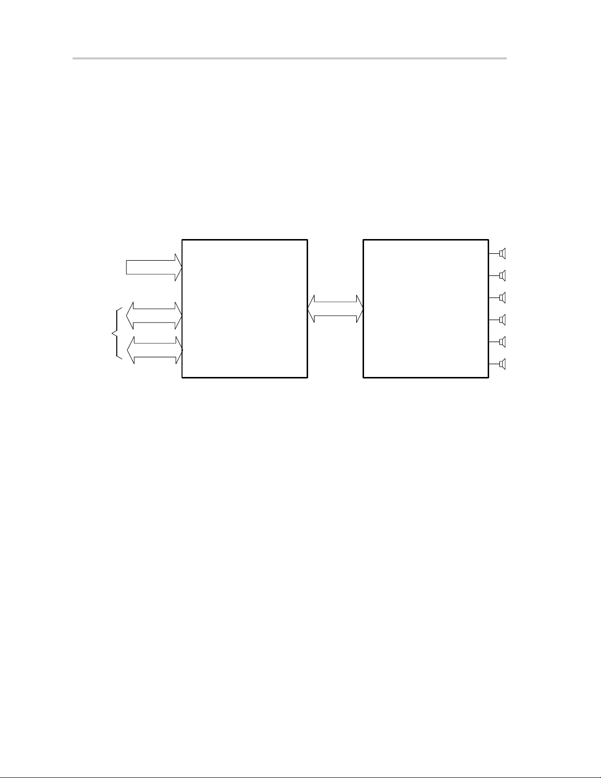
Figure 1–1.TDAA System With TAS5026REF/TAS5036 and TAS5110D6REF Modules
Digital
Audio
Interface
Control
Interface
I2C Bus
I2C Bus
Control Interface
TAS5026REF/TAS5036REF
Module
PWM Interface
TAS5110D6REF
Module
The TAS5026 processor is a two-level PCM-to-PWM modulator and the
TAS5036 processor is a three-level modulator.
1-2
Page 11
1.2 PCB Key Map
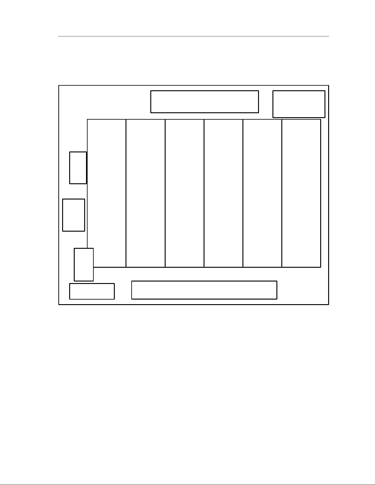
The physical structure for the TAS5110D6REF is illustrated in Figure 1–2.
Figure 1–2.Physical Structure for the TAS5110D6REF (Rough Outline)
PCB Key Map
J150
PSU Interface
J160
Interface
PSU Control
3.3-V Linear
LED Indicators
Left Front Speaker
Output Stage Channel 1
Regulator
J240, J280, J340, J380, J440, and J480
Loudspeaker Outputs
Right Front Speaker
Output Stage Channel 2
Left Rear Speaker
Output Stage Channel 3
TAS5110D6REF
J100
PWM Interface
Right Rear Speaker
Output Stage Channel 4
Center Speaker
Output Stage Channel 5
J110
Subwoofer Output
(Line Level)
Subwoofer
Output Stage Channel 6
Introduction
1-3
Page 12

PCB Key Map
1.3 Short-Circuit Protection and Fault Reporting Circuitry
The TAS5110 is a self-protecting device that provides device fault reporting
(including over-temperature protect and short-circuit protection).
1.3.1 Device Fault Reporting
The ERR0, ERR1, and SHUTDOWN outputs from TAS5110 indicates the
device conditions shown in Table 1–1. The device fault reporting outputs are
open-drain outputs.
Table 1–1.Device Fault Reporting
SHUTDOWN ERR0 ERR1 DEVICE CONDITION
0 0 0 Illegal PWM input state
0 0 1 Short-circuit protect
0 1 0 Over temperature protect
0 1 1 Low regulator voltage protect
1 0 0 Reserved
1 0 1 Reserved
1 1 0 High temperature warning
1 1 1 Normal operation
1.3.2 Short-Circuit Protection
The short-circuit protect error condition latches the T AS5110 in the shutdown
mode:
- H-bridge outputs (OUTPUTA and OUTPUTB) are in a high-impedance
state (Hi-Z state).
- SHUTDOWN is asserted low.
- ERR0 is high and ERR1 is asserted low.
- The H-bridge outputs remains in a Hi-Z state until the device is reset
(RESET
The TAS5110 is not designed for driving load impedance less than 4 Ω (at
20-Vdc output stage supply), where the internal current limit protection is
activated at high power levels.
1.3.3 Auto Recovery System
Together with a PWM processor from Texas Instruments (e.g., the TAS5026
or the TAS5036), the TAS5110 can be configured in autorecovery mode. The
SHUTDOWN
ERR_RCVY
pin asserted low).
signal from the T AS5110 is in autorecovery mode connected to
at the PWM processor.
1-4
The short-circuit protect error condition results in the following autorecovery
sequence:
Page 13
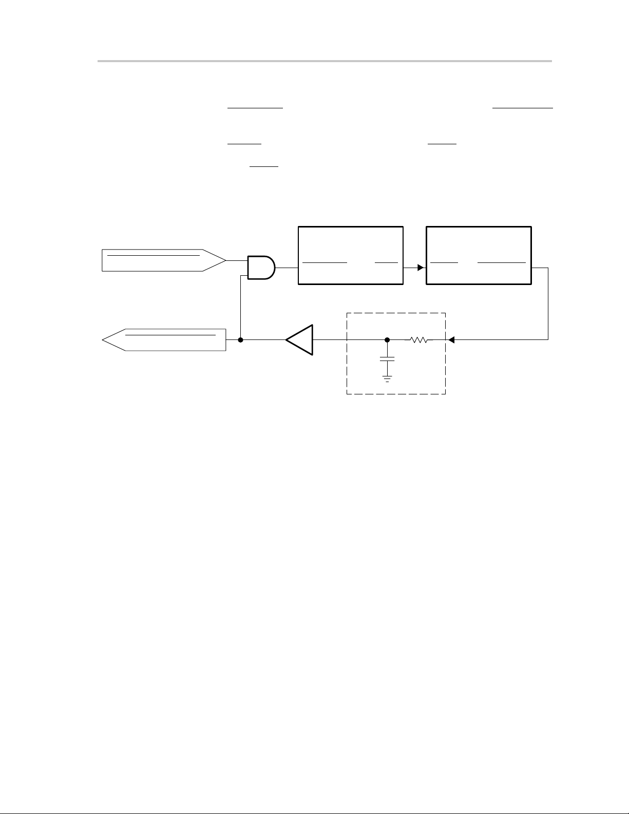
- H-bridge outputs (OUTPUTA and OUTPUTB) are in a high-impedance
state (Hi-Z state).
- ERR_RCVY at the PWM processor is forced low by the SHUTDOWN
signal.
- RESET at the TAS5110 is forced low by the VALID signal.
- The VALID signal goes high after 4 ms and then the TAS5110 starts
switching again.
Figure 1–3.Auto Recovery Loop
PCB Key Map
EXTERNAL_ERR_RCVY
SHUTDOWN-FILTERED
AND
Gate
ERR_RCVY
Buffer
PWM Processor
Low-Pass Filter
VALID
RESET
TAS5110
SHUTDOWN
The autorecovery loop is closed when the TAS5110D6REF board is
connected to the TAS5026REF or TAS5036REF module.
Introduction
1-5
Page 14

1-6
Page 15

Chapter 2
System Interfaces
This chapter describes the TAS5110D6REF system interfaces.
Topic Page
2.1 PSU Interface (J150) 2-2. . . . . . . . . . . . . . . . . . . . . . . . . . . . . . . . . . . . . . . . . . .
2.2 PSU Control Interface (J160) 2-3. . . . . . . . . . . . . . . . . . . . . . . . . . . . . . . . . . .
2.3 Loudspeaker Connectors (J240, J280, J340, J440, and J480) 2-3. . . . .
2.4 PWM Interface (J100) 2-4. . . . . . . . . . . . . . . . . . . . . . . . . . . . . . . . . . . . . . . . . .
System Interfaces
2-1
Page 16

PSU Interface (J150)
2.1 PSU Interface (J150)
The TAS5110D6DAD board must be powered from external power supplies.
High-end audio performance requires a stabilized power supply with low ripple
voltage and low output impedance.
Note:
The length of the power-supply cable must be minimized. Increasing the
impedance of the PSU cable is equal to increasing the distortion for the
amplifier at high output levels and low frequencies.
The maximum output stage supply voltage depends on the speaker load
resistance. See the recommended maximum supply voltage in Chapter 4.
Supply voltage for output stage 0 V – 20 V 0 V – 26.5 V 0 V – 26.5 V
Supply voltage for gate drive 22 V (min 16.5 V, max 26.5 V)
Supply voltage for control 5 V (min 4.5 V, max 5.3 V)
The recommended T AS51 10 power-up sequence is shown in Figure 2–1. For
proper T AS5110 operation, the RESET signal should be kept low during power
up. RESET
linear regulator (U170).
Description RL = 4 Ω RL = 6 Ω RL = 8 Ω
is pulled low during power up for 100 ms by the onboard low-drop
Figure 2–1.Recommended TAS5110 Power-Up Sequence
Control Supply (3.3 V)
Gate-Drive Supply
Output Stage Supply
RESET
>1 ms
Figure 2–2.Pin Numbers at the PSU Interface (Top View)
4
3
2
1
Table 2–1.J150 Pin Description
Pin No. Net Name at Schematic Description
1 Power output stage H-bridge supply voltage
2 GND Ground
3 Gate-drive supply Gate-drive supply voltage (I ≈ 90 mA)
4 5 V Control supply voltage (I ≈ 100 mA)
2-2
Page 17

2.2 PSU Control Interface (J160)
This interface is not used in this board.
Figure 2–3.Pin Numbers at the PSU Control Interface
5
4
3
2
1
Table 2–2.PSU Control Interface Pin Connections
Pin No. Pin Description Net Name at TAS5110D6REF Schematic
1 For future use
2 For future use
3 Ground GND
4 System reset
(bidirectional)
5 For future use V-HBRIDGE-CONTROL
PSU Control Interface (J160)
RESET
2.3 Loudspeaker Connectors (J240, J280, J340, J380, J440, and J480)
Figure 2–4.Pin Numbers at the Loudspeaker Connectors
2
1
Table 2–3.Description of Loudspeaker Connectors
Pin No. Pin Description
2 Speaker positive output terminal
1 Speaker negative output terminal
Caution
Both positive and negative speaker outputs are floating and may not be
connected to ground (e.g., through an oscilloscope).
System Interfaces
2-3
Page 18

PWM Interface (J100)
2.4 PWM Interface (J100)
This interface connects the TAS5110D6REF board to the PWM processor
module (e.g., TAS5026REF).
Figure 2–5.Pin Numbers at PWM Interface (J100)
2
64 89710 12
31 5
1614 18
1311 15
20 22
1917
2321 25
2624 28
30 32
2927
3331 35
3634 38
40 42
3937
Connector: 50 positions, 2,54-mm pitch, double row IDC connector
(Multicomp MC9A12–5034).
Table 2–4.J100 Pin Description
Pin No. Net Name Description
01 V-HBRIDGE-CONTROL For future use
02 GND Ground
03 PWM–AP–1
04 PWM–AM–1 Channel 1 PWM input (differential –) – positive H-bridge side
05 VALID–1 V alid channel 1
06 PWM–BM–1 Channel 1 PWM input (differential –) – negative H-bridge side
07 PWM–BP–1 Channel 1 PWM input (differential +) – negative H-bridge side
08 GND Ground
09 PWM–AP–2 Channel 2 PWM input (differential +) – positive H-bridge side
10 PWM–AM–2 Channel 2 PWM input (differential –) – positive H-bridge side
11 VALID–2 Valid channel 2
12 PWM–BM–2 Channel 2 PWM input (differential –) – negative H-bridge side
13 PWM–BP–2 Channel 2 PWM input (differential +) – negative H-bridge side
14 GND Ground
15 PWM–AP–3 Channel 3 PWM input (differential +) – positive H-bridge side
16 PWM–AM–3 Channel 3 PWM input (differential –) – positive H-bridge side
17 VALID–3 V alid channel 3
18 PWM–BM–3 Channel 3 PWM input (differential –) – negative H-bridge side
19 PWM–BP–3 Channel 3 PWM input (differential +) – negative H-bridge side
20 GND Ground
21 PWM–AP–4 Channel 4 PWM input (differential +) – positive H-bridge side
22 PWM–AM–4 Channel 4 PWM input (differential –) – positive H-bridge side
23 VALID–4 V alid channel 4
24 PWM–BM–4 Channel 4 PWM input (differential –) – negative H-bridge side
25 PWM–BP–4 Channel 4 PWM input (differential +) – negative H-bridge side
26 GND Ground
27 PWM–AP–5 Channel 5 PWM input (differential +) – positive H-bridge side
Channel 1 PWM input (differential +) – positive H-bridge side
4341 45
4644 48
50
4947
2-4
Page 19

PWM Interface (J100)
Table 2–4. J100 Pin Description (Continued)
Pin No. Net Name Description
28 PWM–AM–5 Channel 5 PWM input (differential –) – positive H-bridge side
29 VALID–5 V alid channel 5
30 PWM–BM–5 Channel 5 PWM input (differential –) – negative H-bridge side
31 PWM–BP–5 Channel 5 PWM input (differential +) – negative H-bridge side
32 GND Ground
33 PWM–AP–6 Channel 6 PWM input (differential +) – positive H-bridge side
34 PWM–AM–6 Channel 6 PWM input (differential –) – positive H-bridge side
35 VALID–6 V alid channel 6
36 PWM–BM–6 Channel 6 PWM input (differential –) – negative H-bridge side
37 PWM–BP–6 Channel 6 PWM input (differential +) – negative H-bridge side
38 SD–E1 Shutdown group 1 (center + left and right front speakers)
39 SD–E2 Shutdown group 2 (subwoofer + left and right rear speakers)
40 ERROR0 Error signal ERR0 from TAS5110
41 ERROR1 Error signal ERR1 from TAS5110
42 RESET System reset (bidirectional)
43 PSU–COMP–2 For future use
44 PSU–COMP–1 For future use
45 Not Used For future use
46 Not Used For future use
47 +3.3V 3.3-V supply voltage for the modulator module (e.g., the T AS5026REF)
48 GND Ground
49 +5V 5-V supply voltage
50 +5V 5-V supply voltage
System Interfaces
2-5
Page 20

2-6
Page 21

Chapter 3
Electrical Specifications and Typical
Characteristics Graphs
This chapter contains the electrical specifications and the typical
characteristics graphs.
Topic Page
3.1 Electrical Specifications 3-2. . . . . . . . . . . . . . . . . . . . . . . . . . . . . . . . . . . . . . .
3.2 Physical Specifications 3-2. . . . . . . . . . . . . . . . . . . . . . . . . . . . . . . . . . . . . . . .
3.3 T ypical Characteristics Graphs 3-3. . . . . . . . . . . . . . . . . . . . . . . . . . . . . . . . .
Electrical Specifications and T ypical Characteristics Graphs
3-1
Page 22

TAS5110D6REF Electrical Specifications
3.1 TAS5110D6REF Electrical Specifications
General T est Conditions
PARAMETER TEST CONDITIONS MIN TYP MAX UNIT
Output stage power supply
Gate drive power supply 26.5 VDC
Load impedance 6 Ω
S/PDIF sampling
frequency
PWM processor TAS5026REF (Rev 5) board
Electrical Data
Maximum output power
(10% THD)
Maximum output power
(unclipped)
Continous maximum
output power
Rated load impedance
Maximum peak current 1-kHz burst 6 A
Damping factor 1 kHz, load = 8 Ω 13
Idle switch loss
Gate-drive current V
5-V supply current TAS5110D6REF + TAS5026REF 85 mA
Audio Data
THD+N, 1 W 1 kHz 0.05%
THD+N, 30 W 1 kHz 0.09%
THD+N, 40 W 1 kHz
Dynamic range,
A-weighted
Noise voltage, A-weighted RMS, AES17 filter 260 µV
Channel separation 1 kHz, P
Frequency response DC – 20 kHz, 40 W, 6 Ω ±0.5 dB – 0.1 dB
Note: All electrical and audio specifications are typical values.
†
Heatsink solution is a prototype and has to be optimized for end-product mass production by common engineering practice.
Laboratory power supply
(EA–PS 7065–10A)
26.5 VDC
48 kHz
10% THD+N, 1 kHz,
= 25°C, 6 Ω
T
A
0.15% THD+N, 1 kHz,
T
= 25°C, 6 Ω
A
After 30 minutes preheat of 1/8 max
power in six channels, 10% THD+N, 1
kHz, T
At V
At V
= 25°C, 6 Ω (See Note 1)
A
(POWER-OUTPUT-STAGE)
(POWER-OUTPUT-STAGE)
up to 26.5 V 6 8
up to 20 V 4
Six channels,
V
(POWER-OUTPUT-STAGE)
(GATE-DRIVE-SUPPLY)
= 26.5 V
= 26.5 V 90 mA
50/channel W
40/channel W
2 x 50 W
{
>5 min
4 W
<0.15
%
Ref: rated power, AES17 filter 94 dB
= 30 W 68 dB
OUT
W
Ω
3.2 Physical Specifications
PCB dimensions 105 x 127 mm (4.13 x 5”) Height x Width
Board weight 0,15 kg (0.33 lb) Components + PCB
3-2
Page 23

3.3 Typical Characteristics Graphs
Figure 3–1.THD+N vs Power – Channel 1, 2, 3, 4, 5, and 6
10
Power Supply = 26.5 V DC
5
Load = 6 Ω
Sample Frequency = 48 kHz
Filter = AES17
2
1
0.5
%
0.2
0.1
Channel 3
0.05
0.02
0.01
60m 50100m 200m 500m 1
Channel 5
Channel 2
Channel 4
2
Typical Characteristics Graphs
Channel 6
Channel 1
51020
Figure 3–2.THD+N vs Frequency – Channel 1
10
Power Supply = 26.5 V DC
5
Input Signal = 1 kHz
Load = 6 Ω
Sample Frequency = 48
kHz
2
Filter = AES17
1
0.5
%
0.2
0.1
0.05
10 W
0.02
0.01
20 20k50 100 200 500 1k 2k 5k 10k
20 W
Frequency – Hz
Note: THD+N at high frequencies depends on the output-filter coil material.
40 W
1 W
Electrical Specifications and T ypical Characteristics Graphs
3-3
Page 24

Typical Characteristics Graphs
Figure 3–3.FFT With –60 dB Input Signal – Channel 1
+0
–5
–10
Power Supply = 26.5 V DC
Input Signal = 1 kHz
–15
Load = 6 Ω
–20
Sample Frequency = 48 kHz
–25
Filter = AES17
–30
FFT Size = 16 kΩ
–35
Reference = 15.8 V = Full Scale
–40
–45
–50
–55
–60
d
–65
B
r
–70
–75
A
–80
–85
–90
–95
–100
–105
–110
–115
–120
–125
–130
–135
–140
0 22k1k1 2k 3k 4k 5k 6k 7k 8k 9k 10k 11k 12k 13k 14k 15k 16k 17k 18k 19k 20k 21k
Frequency – Hz
Figure 3–4.Noise Floor – Channel 1
+0
–5
–10
–15
–20
–25
–30
–35
–40
–45
–50
–55
–60
d
–65
B
–70
r
–75
A
–80
–85
–90
–95
–10 0
–10 5
–11 0
–11 5
–12 0
–12 5
–13 0
–13 5
–14 0
Power Supply = 26.5 V DC
Input Signal = 0 F
Load = 6 Ω
Sample Frequency = 48 kHz
FFT Size = 16 kΩ
Reference = 15.8 V = Full Scale
5k
S
85k10k 15k 20k 25k 30k 35k 4 0k 4 5k 50k 55k 60k 65k 70k75k80k
3-4
Page 25

Figure 3–5.Channel Separation vs Frequency – Channel 1
+20
+15
+10
+5
+0
–5
–10
–15
–20
–25
–30
d
–35
B
r
–40
A
–45
–50
–55
–60
–65
–70
–75
–80
–85
–90
–95
–100
20 30k50 100 200 500 1k 2k 5k 10k 20k
Channel 2
Channel 1
Frequency – Hz
Typical Characteristics Graphs
Power Supply = 26.5 V DC
Load = 6 Ω
Sample Frequency = 48 kHz
Filter = AES17
Reference = 15.8 V = Full Scale
Input Left Channel = 0 F
Input Right Channel = 1 F
S
S
Figure 3–6.Frequency Response – Channel 1
+10
+9
+8
Power Supply = 26.5 V
DC
+7
Input Signal = 1 kHz
+6
Sample Frequency = 48
kHz
+5
+4
+3
+2
+1
d
B
r
–0
A
–1
–2
–3
–4
–5
–6
–7
–8
–9
–10
20 20k50 100 200 500 1k 2k 5k 10k
Frequency – Hz
Figure 3–7.Overcurrent Protection – Channel 1
6-Ω Load
8-Ω Load
4-Ω Load
Electrical Specifications and T ypical Characteristics Graphs
3-5
Page 26

Typical Characteristics Graphs
10
9
Power Supply = 26.5 V DC
8
Input Signal = 1 kHz, 1/39 duty cycle, attenuated to 39%
of full scale
7
Sample Frequency = 48 kHz
6
5
4
3
2
C
U
R
1
R
E
0
N
T
–1
A
–2
–3
–4
–5
–6
–7
–8
–9
–10
38m
1-Ω Load
42m38.5m 39m 39.5m 40m 40.5m 41m 41.5m
3-6
Page 27

Chapter 4
Schematic, Parts List, PCB Specification, and
PCB Layout
The chapter contains the schematic, parts list, PCB specification, and PCB
layout for the TAS5110D6REF.
Schematic, Parts List, PCB Specification, and PCB Layout
4-1
Page 28

INPUT SECTION
TI
TAS5110D6REF
DIGITAL AUDIO GROUP
ALL RIGHTS RESERVED - PATENTS PENDING
TEXAS INSTRUMENTS INCORPORATED
Page 29

Front Speakers
Patents pending in circuitry design and layout (WO99/59241 & WO99/59242).
This circuitry may only be used together with the integrated circuit TAS5100/TAS5110
from Texas Instruments Incorporated.
TI
TAS5110D6REF
DIGITAL AUDIO GROUP
ALL RIGHTS RESERVED - PATENTS PENDING
TEXAS INSTRUMENTS INCORPORATED
Page 30

Rear Speakers
Patents pending in circuitry design and layout (WO99/59241 & WO99/59242).
This circuitry may only be used together with the integrated circuit TAS5100/TAS5110
from Texas Instruments Incorporated.
TI
TAS5110D6REF
DIGITAL AUDIO GROUP
ALL RIGHTS RESERVED - PATENTS PENDING
TEXAS INSTRUMENTS INCORPORATED
Page 31

Center Speaker & Subwoofer
Patents pending in circuitry design and layout (WO99/59241 & WO99/59242).
This circuitry may only be used together with the integrated circuit TAS5100/TAS5110
from Texas Instruments Incorporated.
TI
TAS5110D6REF
DIGITAL AUDIO GROUP
ALL RIGHTS RESERVED - PATENTS PENDING
TEXAS INSTRUMENTS INCORPORATED
Page 32

TAS5110D6REF Parts List
P167-LST-001(4.00) App A
Appendix A Page 1 of 8
Ref Des Part Number Description Housing Manufacturer Manufacturer Part Number
R121 100210000 100R 5% 200 ppm 100-mW metalfilm 0603 BC Components DCT 0603 - 00 5% PA 100R
R122 100210000 100R 5% 200 ppm 100-mW metalfilm 0603 BC Components DCT 0603 - 00 5% PA 100R
R131 100210000 100R 5% 200 ppm 100-mW metalfilm 0603 BC Components DCT 0603 - 00 5% PA 100R
R133 100210000 100R 5% 200 ppm 100-mW metalfilm 0603 BC Components DCT 0603 - 00 5% PA 100R
R140 100210000 100R 5% 200 ppm 100-mW metalfilm 0603 BC Components DCT 0603 - 00 5% PA 100R
R141 100210000 100R 5% 200 ppm 100-mW metalfilm 0603 BC Components DCT 0603 - 00 5% PA 100R
R117 100210010 1k00 5% 200 ppm 100-mW metalfilm 0603 BC Components DCT 0603 - 00 5% PA 1k00
R118 100210010 1k00 5% 200 ppm 100-mW metalfilm 0603 BC Components DCT 0603 - 00 5% PA 1k00
R124 100210010 1k00 5% 200 ppm 100-mW metalfilm 0603 BC Components DCT 0603 - 00 5% PA 1k00
R125 100210010 1k00 5% 200 ppm 100-mW metalfilm 0603 BC Components DCT 0603 - 00 5% PA 1k00
R126 100210010 1k00 5% 200 ppm 100-mW metalfilm 0603 BC Components DCT 0603 - 00 5% PA 1k00
R130 100210010 1k00 5% 200 ppm 100-mW metalfilm 0603 BC Components DCT 0603 - 00 5% PA 1k00
R132 100210010 1k00 5% 200 ppm 100-mW metalfilm 0603 BC Components DCT 0603 - 00 5% PA 1k00
R110 100210020 10k0 5% 200 ppm 100-mW metalfilm 0603 BC Components DCT 0603 - 00 5% PA 10k0
R111 100210020 10k0 5% 200 ppm 100-mW metalfilm 0603 BC Components DCT 0603 - 00 5% PA 10k0
R116 100210030 100k 5% 200 ppm 100-mW metalfilm 0603 BC Components DCT 0603 - 00 5% PA 100k
R170 100210030 100k 5% 200 ppm 100-mW metalfilm 0603 BC Components DCT 0603 - 00 5% PA 100k
R240 100210080 1R0 5% 300 ppm 100-mW metalfilm 0603 BC Components DCT 0603 -00 5% PA 1R0
R241 100210080 1R0 5% 300 ppm 100-mW metalfilm 0603 BC Components DCT 0603 -00 5% PA 1R0
R280 100210080 1R0 5% 300 ppm 100-mW metalfilm 0603 BC Components DCT 0603 -00 5% PA 1R0
R282 100210080 1R0 5% 300 ppm 100-mW metalfilm 0603 BC Components DCT 0603 -00 5% PA 1R0
R340 100210080 1R0 5% 300 ppm 100-mW metalfilm 0603 BC Components DCT 0603 -00 5% PA 1R0
R341 100210080 1R0 5% 300 ppm 100-mW metalfilm 0603 BC Components DCT 0603 -00 5% PA 1R0
R380 100210080 1R0 5% 300 ppm 100-mW metalfilm 0603 BC Components DCT 0603 -00 5% PA 1R0
R382 100210080 1R0 5% 300 ppm 100-mW metalfilm 0603 BC Components DCT 0603 -00 5% PA 1R0
R440 100210080 1R0 5% 300 ppm 100-mW metalfilm 0603 BC Components DCT 0603 -00 5% PA 1R0
R441 100210080 1R0 5% 300 ppm 100-mW metalfilm 0603 BC Components DCT 0603 -00 5% PA 1R0
R480 100210080 1R0 5% 300 ppm 100-mW metalfilm 0603 BC Components DCT 0603 -00 5% PA 1R0
R482 100210080 1R0 5% 300 ppm 100-mW metalfilm 0603 BC Components DCT 0603 -00 5% PA 1R0
R200 100210090 10R0 5% 200 ppm 100-mW metalfilm 0603 BC Components DCT 0603 -00 5% PA 10R
R201 100210090 10R0 5% 200 ppm 100-mW metalfilm 0603 BC Components DCT 0603 -00 5% PA 10R
R220 100210090 10R0 5% 200 ppm 100-mW metalfilm 0603 BC Components DCT 0603 -00 5% PA 10R
R221 100210090 10R0 5% 200 ppm 100-mW metalfilm 0603 BC Components DCT 0603 -00 5% PA 10R
R300 100210090 10R0 5% 200 ppm 100-mW metalfilm 0603 BC Components DCT 0603 -00 5% PA 10R
R301 100210090 10R0 5% 200 ppm 100-mW metalfilm 0603 BC Components DCT 0603 -00 5% PA 10R
R320 100210090 10R0 5% 200 ppm 100-mW metalfilm 0603 BC Components DCT 0603 -00 5% PA 10R
R321 100210090 10R0 5% 200 ppm 100-mW metalfilm 0603 BC Components DCT 0603 -00 5% PA 10R
R400 100210090 10R0 5% 200 ppm 100-mW metalfilm 0603 BC Components DCT 0603 -00 5% PA 10R
R401 100210090 10R0 5% 200 ppm 100-mW metalfilm 0603 BC Components DCT 0603 -00 5% PA 10R
All rights belongs to Texas Instruments Incorporated
Texas Instruments Incorporated
Page 33

TAS5110D6REF Parts List
P167-LST-001(4.00) App A
Appendix A Page 2 of 8
Ref Des Part Number Description Housing Manufacturer Manufacturer Part Number
R420 100210090 10R0 5% 200 ppm 100-mW metalfilm 0603 BC Components DCT 0603 -00 5% PA 10R
R421 100210090 10R0 5% 200 ppm 100-mW metalfilm 0603 BC Components DCT 0603 -00 5% PA 10R
R202 100213020 13k0 5% 200 ppm 100-mW metalfilm 0603 BC Components DCT 0603 - 00 5% PA 13k0
R203 100213020 13k0 5% 200 ppm 100-mW metalfilm 0603 BC Components DCT 0603 - 00 5% PA 13k0
R222 100213020 13k0 5% 200 ppm 100-mW metalfilm 0603 BC Components DCT 0603 - 00 5% PA 13k0
R223 100213020 13k0 5% 200 ppm 100-mW metalfilm 0603 BC Components DCT 0603 - 00 5% PA 13k0
R302 100213020 13k0 5% 200 ppm 100-mW metalfilm 0603 BC Components DCT 0603 - 00 5% PA 13k0
R303 100213020 13k0 5% 200 ppm 100-mW metalfilm 0603 BC Components DCT 0603 - 00 5% PA 13k0
R322 100213020 13k0 5% 200 ppm 100-mW metalfilm 0603 BC Components DCT 0603 - 00 5% PA 13k0
R323 100213020 13k0 5% 200 ppm 100-mW metalfilm 0603 BC Components DCT 0603 - 00 5% PA 13k0
R402 100213020 13k0 5% 200 ppm 100-mW metalfilm 0603 BC Components DCT 0603 - 00 5% PA 13k0
R403 100213020 13k0 5% 200 ppm 100-mW metalfilm 0603 BC Components DCT 0603 - 00 5% PA 13k0
R422 100213020 13k0 5% 200 ppm 100-mW metalfilm 0603 BC Components DCT 0603 - 00 5% PA 13k0
R423 100213020 13k0 5% 200 ppm 100-mW metalfilm 0603 BC Components DCT 0603 - 00 5% PA 13k0
R120 100222000 220R 5% 200 ppm 100-mW metalfilm 0603 BC Components DCT 0603 -00 5% PA 220R
R114 100222020 22k 5% 200 ppm 100-mW metalfilm 0603 BC Components DCT 0603 -00 5% PA 22k
R115 100222020 22k 5% 200 ppm 100-mW metalfilm 0603 BC Components DCT 0603 -00 5% PA 22k
R123 100233000 330R 5% 200 ppm 100-mW 0603 BC Components DCT 0603 -00 5% PA 330R
R260 100233080 3R30 5% 300 ppm 100-mW metalfilm 0603 BC Components DCT 0603 -00 5% PA 3R30
R360 100233080 3R30 5% 300 ppm 100-mW metalfilm 0603 BC Components DCT 0603 -00 5% PA 3R30
R460 100233080 3R30 5% 300 ppm 100-mW metalfilm 0603 BC Components DCT 0603 -00 5% PA 3R30
R112 100247020 47k0 5% 200 ppm 100-mW metalfilm 0603 BC Components DCT 0603 -00 5% PA 47k0
R113 100247020 47k0 5% 200 ppm 100-mW metalfilm 0603 BC Components DCT 0603 -00 5% PA 47k0
R204 100315080 1R50 5% 100 ppm 250-mW metalfilm RC3715 Beychlag MMA0204-100 5% BL 1R50
R205 100315080 1R50 5% 100 ppm 250-mW metalfilm RC3715 Beychlag MMA0204-100 5% BL 1R50
R224 100315080 1R50 5% 100 ppm 250-mW metalfilm RC3715 Beychlag MMA0204-100 5% BL 1R50
R225 100315080 1R50 5% 100 ppm 250-mW metalfilm RC3715 Beychlag MMA0204-100 5% BL 1R50
R304 100315080 1R50 5% 100 ppm 250-mW metalfilm RC3715 Beychlag MMA0204-100 5% BL 1R50
R305 100315080 1R50 5% 100 ppm 250-mW metalfilm RC3715 Beychlag MMA0204-100 5% BL 1R50
R324 100315080 1R50 5% 100 ppm 250-mW metalfilm RC3715 Beychlag MMA0204-100 5% BL 1R50
R325 100315080 1R50 5% 100 ppm 250-mW metalfilm RC3715 Beychlag MMA0204-100 5% BL 1R50
R404 100315080 1R50 5% 100 ppm 250-mW metalfilm RC3715 Beychlag MMA0204-100 5% BL 1R50
R405 100315080 1R50 5% 100 ppm 250-mW metalfilm RC3715 Beychlag MMA0204-100 5% BL 1R50
R424 100315080 1R50 5% 100 ppm 250-mW metalfilm RC3715 Beychlag MMA0204-100 5% BL 1R50
R425 100315080 1R50 5% 100 ppm 250-mW metalfilm RC3715 Beychlag MMA0204-100 5% BL 1R50
C202 200011040 100nF 50V 20% X7R 0805 Philips 2222 580 16741
C203 200011040 100nF 50V 20% X7R 0805 Philips 2222 580 16741
C205 200011040 100nF 50V 20% X7R 0805 Philips 2222 580 16741
C207 200011040 100nF 50V 20% X7R 0805 Philips 2222 580 16741
All rights belongs to Texas Instruments Incorporated
Texas Instruments Incorporated
Page 34

TAS5110D6REF Parts List
P167-LST-001(4.00) App A
Appendix A Page 3 of 8
Ref Des Part Number Description Housing Manufacturer Manufacturer Part Number
C208 200011040 100 nF 50 V 20% X7R 0805 Philips 2222 580 16741
C222 200011040 100 nF 50 V 20% X7R 0805 Philips 2222 580 16741
C223 200011040 100 nF 50 V 20% X7R 0805 Philips 2222 580 16741
C225 200011040 100 nF 50 V 20% X7R 0805 Philips 2222 580 16741
C227 200011040 100 nF 50 V 20% X7R 0805 Philips 2222 580 16741
C302 200011040 100 nF 50 V 20% X7R 0805 Philips 2222 580 16741
C303 200011040 100 nF 50 V 20% X7R 0805 Philips 2222 580 16741
C305 200011040 100 nF 50 V 20% X7R 0805 Philips 2222 580 16741
C307 200011040 100 nF 50 V 20% X7R 0805 Philips 2222 580 16741
C308 200011040 100 nF 50 V 20% X7R 0805 Philips 2222 580 16741
C322 200011040 100 nF 50 V 20% X7R 0805 Philips 2222 580 16741
C323 200011040 100 nF 50 V 20% X7R 0805 Philips 2222 580 16741
C325 200011040 100 nF 50 V 20% X7R 0805 Philips 2222 580 16741
C327 200011040 100 nF 50 V 20% X7R 0805 Philips 2222 580 16741
C328 200011040 100 nF 50 V 20% X7R 0805 Philips 2222 580 16741
C402 200011040 100 nF 50 V 20% X7R 0805 Philips 2222 580 16741
C403 200011040 100 nF 50 V 20% X7R 0805 Philips 2222 580 16741
C405 200011040 100 nF 50 V 20% X7R 0805 Philips 2222 580 16741
C407 200011040 100 nF 50 V 20% X7R 0805 Philips 2222 580 16741
C408 200011040 100 nF 50 V 20% X7R 0805 Philips 2222 580 16741
C422 200011040 100 nF 50 V 20% X7R 0805 Philips 2222 580 16741
C423 200011040 100 nF 50 V 20% X7R 0805 Philips 2222 580 16741
C425 200011040 100 nF 50 V 20% X7R 0805 Philips 2222 580 16741
C427 200011040 100 nF 50 V 20% X7R 0805 Philips 2222 580 16741
C428 200011040 100 nF 50 V 20% X7R 0805 Philips 2222 580 16741
C429 200011040 100 nF 50 V 20% X7R 0805 Philips 2222 580 16741
R228 200011040 100 nF 50 V 20% X7R 0805 Philips 2222 580 16741
C204 200023330 33 nF 100 V 20% X7R 1206 Philips 2222 601 16743
C206 200023330 33 nF 100 V 20% X7R 1206 Philips 2222 601 16743
C224 200023330 33 nF 100 V 20% X7R 1206 Philips 2222 601 16743
C226 200023330 33 nF 100 V 20% X7R 1206 Philips 2222 601 16743
C304 200023330 33 nF 100 V 20% X7R 1206 Philips 2222 601 16743
C306 200023330 33 nF 100 V 20% X7R 1206 Philips 2222 601 16743
C324 200023330 33 nF 100 V 20% X7R 1206 Philips 2222 601 16743
C326 200023330 33 nF 100 V 20% X7R 1206 Philips 2222 601 16743
C404 200023330 33 nF 100 V 20% X7R 1206 Philips 2222 601 16743
C406 200023330 33 nF 100 V 20% X7R 1206 Philips 2222 601 16743
C424 200023330 33 nF 100 V 20% X7R 1206 Philips 2222 601 16743
C426 200023330 33 nF 100 V 20% X7R 1206 Philips 2222 601 16743
All rights belongs to Texas Instruments Incorporated
Texas Instruments Incorporated
Page 35

TAS5110D6REF Parts List
P167-LST-001(4.00) App A
Appendix A Page 4 of 8
Ref Des Part Number Description Housing Manufacturer Manufacturer Part Number
C100 200041060 10 uF 16 V 20% LYT LY4x5SMD Panasonic ECE V 1C A 100 SR
C101 200041060 10 uF 16 V 20% LYT LY4x5SMD Panasonic ECE V 1C A 100 SR
C115 200041060 10 uF 16 V 20% LYT LY4x5SMD Panasonic ECE V 1C A 100 SR
C117 200041060 10 uF 16 V 20% LYT LY4x5SMD Panasonic ECE V 1C A 100 SR
C170 200041060 10 uF 16 V 20% LYT LY4x5SMD Panasonic ECE V 1C A 100 SR
C172 200041060 10 uF 16 V 20% LYT LY4x5SMD Panasonic ECE V 1C A 100 SR
C150 200044750 4.7 uF 35 V 20% 105°C 8R LY4x5SMD Philips BCC2222-153-60478
C245 200051030 10 nF 50 V 20% X7R 0603 KEMET C0603C103M5RAC
C246 200051030 10 nF 50 V 20% X7R 0603 KEMET C0603C103M5RAC
C263 200051030 10 nF 50 V 20% X7R 0603 KEMET C0603C103M5RAC
C285 200051030 10 nF 50 V 20% X7R 0603 KEMET C0603C103M5RAC
C286 200051030 10 nF 50 V 20% X7R 0603 KEMET C0603C103M5RAC
C345 200051030 10 nF 50 V 20% X7R 0603 KEMET C0603C103M5RAC
C346 200051030 10 nF 50 V 20% X7R 0603 KEMET C0603C103M5RAC
C363 200051030 10 nF 50 V 20% X7R 0603 KEMET C0603C103M5RAC
C385 200051030 10 nF 50 V 20% X7R 0603 KEMET C0603C103M5RAC
C386 200051030 10 nF 50 V 20% X7R 0603 KEMET C0603C103M5RAC
C445 200051030 10 nF 50 V 20% X7R 0603 KEMET C0603C103M5RAC
C446 200051030 10 nF 50 V 20% X7R 0603 KEMET C0603C103M5RAC
C463 200051030 10 nF 50 V 20% X7R 0603 KEMET C0603C103M5RAC
C485 200051030 10 nF 50 V 20% X7R 0603 KEMET C0603C103M5RAC
C486 200051030 10 nF 50 V 20% X7R 0603 KEMET C0603C103M5RAC
C114 200051040 100 nF 16 V 20% X7R 0603 KEMET C0603C104M4RAC
C116 200051040 100 nF 16 V 20% X7R 0603 KEMET C0603C104M4RAC
C171 200051040 100 nF 16 V 20% X7R 0603 KEMET C0603C104M4RAC
C173 200051040 100 nF 16 V 20% X7R 0603 KEMET C0603C104M4RAC
C201 200051040 100 nF 16 V 20% X7R 0603 KEMET C0603C104M4RAC
C221 200051040 100 nF 16 V 20% X7R 0603 KEMET C0603C104M4RAC
C301 200051040 100 nF 16 V 20% X7R 0603 KEMET C0603C104M4RAC
C321 200051040 100 nF 16 V 20% X7R 0603 KEMET C0603C104M4RAC
C401 200051040 100 nF 16 V 20% X7R 0603 KEMET C0603C104M4RAC
C421 200051040 100 nF 16 V 20% X7R 0603 KEMET C0603C104M4RAC
C110 200052230 22 nF 50 V 20% X7R 0603 KEMET C0603C223M3RAC
C111 200052230 22 nF 50 V 20% X7R 0603 KEMET C0603C223M3RAC
C112 200054730 47 nF 16 V 20% X7R 0603 KEMET C0603C473M2RAC
C113 200054730 47 nF 16 V 20% X7R 0603 KEMET C0603C473M2RAC
C200 200061010 100 pF 50 V 10% NP0 0603 KEMET C0603C101K5GAC
C220 200061010 100 pF 50 V 10% NP0 0603 KEMET C0603C101K5GAC
C300 200061010 100 pF 50 V 10% NP0 0603 KEMET C0603C101K5GAC
All rights belongs to Texas Instruments Incorporated
Texas Instruments Incorporated
Page 36

TOKIN
TOKIN
TOKIN
TOKIN
TOKIN
TOKIN
TOKIN
TOKIN
TOKIN
TOKIN
TOKIN
TAS5110D6REF Parts List
P167-LST-001(4.00) App A
Appendix A Page 5 of 8
Ref Des Part Number Description Housing Manufacturer Manufacturer Part Number
C320 200061010 100 pF 50 V 10% NP0 0603 KEMET C0603C101K5GAC
C400 200061010 100 pF 50 V 10% NP0 0603 KEMET C0603C101K5GAC
C420 200061010 100 pF 50 V 10% NP0 0603 KEMET C0603C101K5GAC
C130 200061020 1 nF 10% 50 V NP0 0603 KEMET C0603C102K5GAC
C131 200061020 1 nF 10% 50 V NP0 0603 KEMET C0603C102K5GAC
C140 200061020 1 nF 10% 50 V NP0 0603 KEMET C0603C102K5GAC
C141 200061020 1 nF 10% 50 V NP0 0603 KEMET C0603C102K5GAC
C262 200061020 1 nF 10% 50 V NP0 0603 KEMET C0603C102K5GAC
C362 200061020 1 nF 10% 50 V NP0 0603 KEMET C0603C102K5GAC
C462 200061020 1 nF 10% 50 V NP0 0603 KEMET C0603C102K5GAC
C260 250041081 1000 uF 35 V 20% low ESR C7M5PD18 Panasonic EEUFC1V102
C261 250041081 1000 uF 35 V 20% low ESR C7M5PD18 Panasonic EEUFC1V102
C360 250041081 1000 uF 35 V 20% low ESR C7M5PD18 Panasonic EEUFC1V102
C361 250041081 1000 uF 35 V 20% low ESR C7M5PD18 Panasonic EEUFC1V102
C460 250041081 1000 uF 35 V 20% low ESR C7M5PD18 Panasonic EEUFC1V102
C461 250041081 1000 uF 35 V 20% low ESR C7M5PD18 Panasonic EEUFC1V102
C240 270021051 1 uF 63 V 10% polyester C3B2 Wima MKS4 1uF 63V 10% PCM7.5
C241 270021051 1 uF 63 V 10% polyester C3B2 Wima MKS4 1uF 63V 10% PCM7.5
C280 270021051 1 uF 63 V 10% polyester C3B2 Wima MKS4 1uF 63V 10% PCM7.5
C281 270021051 1 uF 63 V 10% polyester C3B2 Wima MKS4 1uF 63V 10% PCM7.5
C340 270021051 1 uF 63 V 10% polyester C3B2 Wima MKS4 1uF 63V 10% PCM7.5
C341 270021051 1 uF 63 V 10% polyester C3B2 Wima MKS4 1uF 63V 10% PCM7.5
C380 270021051 1 uF 63 V 10% polyester C3B2 Wima MKS4 1uF 63V 10% PCM7.5
C381 270021051 1 uF 63 V 10% polyester C3B2 Wima MKS4 1uF 63V 10% PCM7.5
C440 270021051 1 uF 63 V 10% polyester C3B2 Wima MKS4 1uF 63V 10% PCM7.5
C441 270021051 1 uF 63 V 10% polyester C3B2 Wima MKS4 1uF 63V 10% PCM7.5
C480 270021051 1 uF 63 V 10% polyester C3B2 Wima MKS4 1uF 63V 10% PCM7.5
C481 270021051 1 uF 63 V 10% polyester C3B2 Wima MKS4 1uF 63V 10% PCM7.5
L240 350101031 10uH 8A 10% 28mR
L241 350101031 10uH 8A 10% 28mR
L280 350101031 10uH 8A 10% 28mR
L281 350101031 10uH 8A 10% 28mR
L340 350101031 10uH 8A 10% 28mR
L341 350101031 10uH 8A 10% 28mR
L380 350101031 10uH 8A 10% 28mR
L381 350101031 10uH 8A 10% 28mR
L440 350101031 10uH 8A 10% 28mR
L441 350101031 10uH 8A 10% 28mR
L480 350101031 10uH 8A 10% 28mR
SBPSC-11R310-100A
SBPSC-11R310-100A
SBPSC-11R310-100A
SBPSC-11R310-100A
SBPSC-11R310-100A
SBPSC-11R310-100A
SBPSC-11R310-100A
SBPSC-11R310-100A
SBPSC-11R310-100A
SBPSC-11R310-100A
SBPSC-11R310-100A
All rights belongs to Texas Instruments Incorporated
Texas Instruments Incorporated
Page 37

TOKIN
Toshiba
TLSU1008
Toshiba
TLSU1008
Toshiba
TLGU1008
Toshiba
TLYU1008
TDAA PWM Power Output Stage, DAD package
Texas Instruments
TAS5110DAD
TDAA PWM Power Output Stage, DAD package
Texas Instruments
TAS5110DAD
TDAA PWM Power Output Stage, DAD package
Texas Instruments
TAS5110DAD
TDAA PWM Power Output Stage, DAD package
Texas Instruments
TAS5110DAD
TDAA PWM Power Output Stage, DAD package
Texas Instruments
TAS5110DAD
TDAA PWM Power Output Stage, DAD package
Texas Instruments
TAS5110DAD
Texas Instruments
TLV272CDGK
Texas Instruments
Texas Instruments
Texas Instruments
Texas Instruments
TPS75333QPWP
TAS5110D6REF Parts List
P167-LST-001(4.00) App A
Appendix A Page 6 of 8
Ref Des Part Number Description Housing Manufacturer Manufacturer Part Number
L481 350101031 10uH 8A 10% 28mR
LED121 405000810 RED 10mA LED SMD 0603P
LED122 405000810 RED 10mA LED SMD 0603P
LED123 405000820 GREEN 10mA LED SMD 0603P
LED120 405000830 YELLOW 10mA LED SMD 0603P
Q120 425229070 PNP 40V/800 mA small signal transistor SOT-23 Fairchild MMBT2907A
Q121 425229070 PNP 40V/800 mA small signal transistor SOT-23 Fairchild MMBT2907A
Q122 425229070 PNP 40V/800 mA small signal transistor SOT-23 Fairchild MMBT2907A
U200 500051101
U220 500051101
U300 500051101
U320 500051101
U400 500051101
U420 500051101
U111 510102721 Dual RtR Output OPAMP MSOP8
U110 520141261 Dual buffer with output enable, LVC MSOP8
U130 520141261 Dual buffer with output enable, LVC MSOP8
U140 520141261 Dual buffer with output enable, LVC MSOP8
U170 540251330 3.3 V/1.5A low drop Lin. Reg. HTSSOP20
MECH1 600100050 P167-MECH-002 (1.00) GTV P167-MECH-002 (1.00)
MECH2 600100060 P167-MECH-003 (1.00) GTV P167-MECH-003 (1.00)
MECH2 600100070 P167-MECH-004 (1.00) GTV P167-MECH-004 (1.00)
SCREW01 600200010 M3x6 Pozidriv stainless steel screw Bossard BN 31108 M3x6
SCREW02 600200010 M3x6 Pozidriv stainless steel screw Bossard BN 31108 M3x6
SCREW03 600200010 M3x6 Pozidriv stainless steel screw Bossard BN 31108 M3x6
SCREW04 600200020 M3x10 Pozidriv stainless steel screw Bossard BN 31108 M3x10
SCREW05 600200020 M3x10 Pozidriv stainless steel screw Bossard BN 31108 M3x10
SCREW06 600200020 M3x10 Pozidriv stainless steel screw Bossard BN 31108 M3x10
WASHER01 600400010 M3 stainless steel washer Bossard BN 670
WASHER02 600400010 M3 stainless steel washer Bossard BN 670
WASHER03 600400010 M3 stainless steel washer Bossard BN 670
WASHER04 600400010 M3 stainless steel washer Bossard BN 670
WASHER05 600400010 M3 stainless steel washer Bossard BN 670
WASHER06 600400010 M3 stainless steel washer Bossard BN 670
J110 700100021 2 pin 2,54 mm pitch header, friction lock MX2SI Molex 22-27-2021
J160 700100051 5 pin 2,54 mm pitch header, friction lock MX5SI Molex 22-27-2051
J240 700300020 2 Pin 3,96 mm pitch header MY2S JST B 2P-VH
J280 700300020 2 Pin 3,96 mm pitch header MY2S JST B 2P-VH
J340 700300020 2 Pin 3,96 mm pitch header MY2S JST B 2P-VH
HTSSOP32
HTSSOP32
HTSSOP32
HTSSOP32
HTSSOP32
HTSSOP32
SBPSC-11R310-100A
SN74LVC2G126DCT
SN74LVC2G126DCT
SN74LVC2G126DCT
All rights belongs to Texas Instruments Incorporated
Texas Instruments Incorporated
Page 38

Trace
Trace
Trace
TAS5110D6REF Parts List
P167-LST-001(4.00) App A
Appendix A Page 7 of 8
Ref Des Part Number Description Housing Manufacturer Manufacturer Part Number
J380 700300020 2 pin 3,96 mm pitch header MY2S JST B 2P-VH
J440 700300020 2 pin 3,96 mm pitch header MY2S JST B 2P-VH
J480 700300020 2 pin 3,96 mm pitch header MY2S JST B 2P-VH
J150 700300040 4 pin 3,96 mm pitch header MY4S JST B 4P-VH
J100 700820500 Box header straight 50 pin 2,54 mm IDC50 Multicomp MC9A12-5034
PCB 900116710 P167-PCB-001(1.00) Printline P167-PCB-001(1.00)
C132 Deleted Deleted
C133 Deleted Deleted
C134 Deleted Deleted
C209 Deleted Deleted
C229 Deleted Deleted
C309 Deleted Deleted
C329 Deleted Deleted
C409 Deleted Deleted
C242 Not used Not used
C243 Not used Not used
C244 Not used Not used
C282 Not used Not used
C283 Not used Not used
C284 Not used Not used
C342 Not used Not used
C343 Not used Not used
C344 Not used Not used
C382 Not used Not used
C383 Not used Not used
C384 Not used Not used
C442 Not used Not used
C443 Not used Not used
C444 Not used Not used
C482 Not used Not used
C483 Not used Not used
C484 Not used Not used
J101 Not used Not used
J102 Not used Not used
R261 Not used Not used
R262 Not used Not used
L260
L261
L262
A trace in the PCB
A trace in the PCB
A trace in the PCB
All rights belongs to Texas Instruments Incorporated
Texas Instruments Incorporated
Page 39

Trace
Trace
Trace
Trace
Trace
Trace
Trace
Trace
Trace
TAS5110D6REF Parts List
P167-LST-001(4.00) App A
Appendix A Page 8 of 8
Ref Des Part Number Description Housing Manufacturer Manufacturer Part Number
L263
L360
L361
L362
L363
L460
L461
L462
L463
A trace in the PCB
A trace in the PCB
A trace in the PCB
A trace in the PCB
A trace in the PCB
A trace in the PCB
A trace in the PCB
A trace in the PCB
A trace in the PCB
All rights belongs to Texas Instruments Incorporated
Texas Instruments Incorporated
Page 40

TI TAS5110D6REF PCB SPECIFICATION (1.00)
Claus Reckweg
TAS5110D6REF PCB SPECIFICATION
BOARD IDENTIFICATION: P167-PCB-001 (1.00)
BOARD TYPE: Double-sided plated-through board
LAMINATE TYPE: FR4
LAMINATE THICKNESS: 1,6 mm
COPPER THICKNESS: 70 µm (including plating exterior layer)
COPPER PLATING OF HOLES: >25 µm
MINIMUM HOLE DIAMETER 0,3 mm
SILKSCREEN COMPONENT SIDE: White-remove silkscreen from solder area and pretinned areas
SILKSCREEN SOLDER SIDE: None
SOLDER MASK COMPONENT SIDE: Green
SOLDER MASK SOLDER SIDE: Green
PROTECTIVE COATING: Solder coating and chemical silver on free copper
ELECTRICAL TEST: PCB must be electrical tested
MANUFACTURED TO: PERFAG 2E (www.perfag.dk)
APERTURE TABLE: PERFAG 10A (www.perfag.dk)
BOARD SIZE: 105 x 127 mm
Page 1 of 1
Page 41

Page 42

Page 43

Page 44

Page 45

 Loading...