

Page 1

www.ti.com
PurePath Digital™ AUDIO SIX-CHANNEL PWM PROCESSOR
TAS5086
SLES131B – FEBRUARY 2005 – REVISED JUNE 2007
FEATURES
– Full Six-Channel Input and Output Mapping
• Audio Input/Output – Selectable DC Blocking Filters
– Automatic Master Clock Rate and Data • PWM Processing
Sample Rate Detection
– 8 × Oversampling With Fourth-Order Noise
– Four Serial Audio Inputs (Eight Channels) Shaping at 44.1, 48 kHz; 4 × Oversampling
– Support for 32-, 44.1-, 48-, 88.2-, 96-, 176.4-,
and 192-kHz Sampling Rates
– Data Formats: 16-, 20-, or 24-Bit Input Data;
Left-Justified, Right-Justified, and I2S
– 64- or 48-f
Bit-Clock Rate
S
– 128-, 192-, 256-, 384-, and 512-f
Clock Rates (Up to a Maximum of 50 MHz)
– Six PWM Audio Output Channels
– Any Output Channel Can be Mapped to
Any Output Pin
– Supports Single-Ended and Bridge-Tied
Loads
– I2S Serial Audio Output
• Audio Processing
– Volume Control Range of 48 dB to –100 dB
– Master Volume Control from 24 dB to –100
dB in 0.5-dB Increments
– Six Individual Channel Volume Controls
With 24-dB to –100-dB Attenuation in
0.5-dB Increments
– Serial Output Can Be Produced by
Downmix of 5.1-Channel Input or Fourth
Serial Input
– 5.1-Channel Downmix to 2.1 or 3.1 PWM
Output Speaker System
– Integrated Bass Management
– Two Programmable Biquads in Subwoofer
Master
S
at 88.2, 96 kHz; 2 × Oversampling at 176.4,
192 kHz; and 12 × Oversampling at 32 kHz
– ≥ 105-dB Dynamic Range
(TAS5086+TAS5186)
– THD < 0.06% (TAS5086 Only)
– 20-Hz–20-kHz Flat Noise Floor for 44.1-,
48-, 88.2-, 96-, 176.4- and 192-kHz Data
Rates
– Digital De-Emphasis for 32-kHz, 44.1-kHz
and 48-kHz Data Rates
– Intelligent AM Interference Avoidance
System Provides Clear AM Reception
– Optimized PWM Sequence for Click- and
Popless Start and Stop
– Optimized PWM Sequence for Charging of
AC-Coupling Capacitors in Single-Ended
Configurations
– Adjustable Modulation Limit From 93.8% to
99.2%
• General Features
– Automated Operation With Easy-to-Use
Control Interface
– I2C Serial Control Slave Interface
– Control Interface Operational Without
MCLK
– Single 3.3-V Power Supply
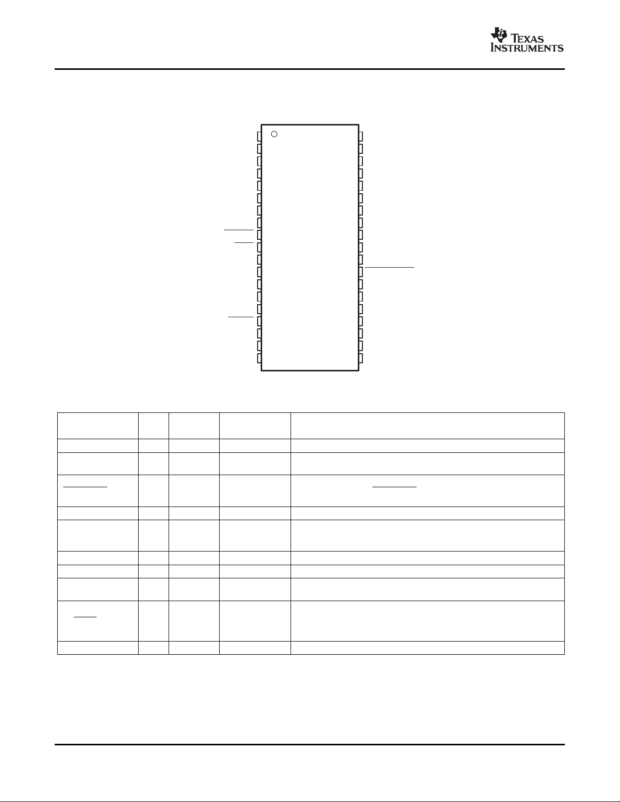
– 38-Pin TSSOP Package
Channel
Please be aware that an important notice concerning availability, standard warranty, and use in critical applications of Texas
Instruments semiconductor products and disclaimers thereto appears at the end of this data sheet.
PurePath Digital is a trademark of Texas Instruments.
All other trademarks are the property of their respective owners.
PRODUCTION DATA information is current as of publication date.
Products conform to specifications per the terms of the Texas
Instruments standard warranty. Production processing does not
necessarily include testing of all parameters.
Copyright © 2005–2007, Texas Instruments Incorporated
Page 2

www.ti.com
TAS5086
SLES131B – FEBRUARY 2005 – REVISED JUNE 2007
These devices have limited built-in ESD protection. The leads should be shorted together or the device placed in conductive foam
during storage or handling to prevent electrostatic damage to the MOS gates.
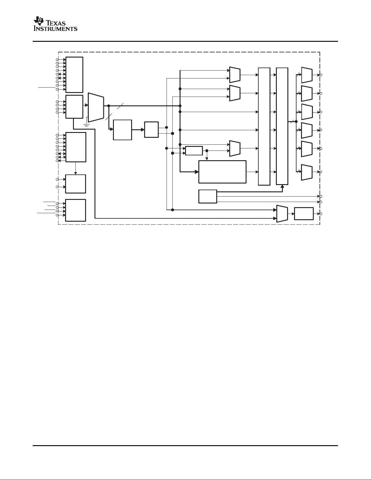
DESCRIPTION
The TAS5086 is a six-channel digital pulse-width modulator (PWM) that provides both advanced performance
and a high level of system integration. The TAS5086 is designed to interface seamlessly with most audio digital
signal processors and MPEG decoders, accepting a wide range of input data and clock formats.
The TAS5086 drives six channels of speakers in either single-ended or bridge-tied load configurations that
accept a 1N + 1 interface format. The TAS5086 also supports 2N + 1 power stages with the use of some
external logic (e.g., TAS5112). Stereo line out in I2S format is available with either a pass-through signal
(SDIN4) or an internal downmix.
The TAS5086 uses AD modulation operating at a 384-kHz switching rate for 32-, 44.1-, 48-, 88.2-, 96-, 176.4-,
and 192-kHz data. The 8 × oversampling, combined with the 4th-order noise shaper, provides a broad, flat noise
floor and excellent dynamic range from 20 Hz to 20 kHz.
The TAS5086 is only an I2C slave device, which always receives MCLK, SCLK, and LRCLK from other system
components. The TAS5086 accepts clock rates of 128, 192, 256, 384, and 512 fS. The TAS5086 accepts a 64-f
master clock for 176.4-kHz and 192-kHz data.
The TAS5086 accepts a 64-f
MCLK ratios of 192 fSand 384 fS.
The TAS5086 is composed of five functional blocks.
• Power supply
• Clock, PLL, and serial data interface
• Serial control interface
• Device control
• PWM section
For detailed application information, see the Using the PurePath Digital PWM Processor application report
(SLEA046 ).
bit clock for all data rates. The TAS5086 also can accept a 48-f
S
SCLK rate for
S
S
Figure 1 shows the functional structure of the TAS5086.
2
Submit Documentation Feedback
Page 3
www.ti.com
Chan.
1 − 6
1− 5
SDIN1
SDIN2
SDIN3
SDIN4
SDA
SCL
PWM1
PWM2
PWM3
PWM4
PWM5
PWM6
VALID1
DVDD
DVSS
DVSS_ESD
VR_DIG
VR_ANA
VR_OSC
AVDD
AVSS_PLL
SDOUT
MCLK
SCLK
LRCLK
PLLFLTP
PLLFLTM
HFCLK
OSCFLT
OSC_RES
1 LF
2 RF
3 LS
4 RS
5 C
1− 6
L’
R’
L’
R’
(L’+R’) / 2
VALID2
1 − 5
Ch
1−6
6
6
6
6
6
6
SDIN4
SDIN4
Downmix
PWM
Control
PDN
RESET
MUTE
VREG_EN
BKNDERR
Channel Six Processing
Bass Management
B0080-01
Power
Supply
Serial
Data
Interface
Channel
Selector
Block
MUX
MUX
Down−
mix
Clock Rate
/Error
Detection
and PLL
Serial
Control
Interface
System
Control
MUX
I2S Serial
Output
MUX
MUX
MUX
Vol
PWM
MUX
MUX
MUX
MUX
MUX
(L’+R’)/2
TAS5086
SLES131B – FEBRUARY 2005 – REVISED JUNE 2007
Figure 1. TAS5086 Functional Block Diagram
Submit Documentation Feedback
3
Page 4
www.ti.com
TAS5086
SLES131B – FEBRUARY 2005 – REVISED JUNE 2007
ABSOLUTE MAXIMUM RATINGS
over operating free-air temperature range (unless otherwise noted)
Supply voltage
Input voltage
Input clamp current, IIK(V
Output clamp current, IOK(V
Operating free-air temperature 0 ° C to 70 ° C
Storage temperature range, T
(1) Stresses beyond those listed under “absolute ratings” may cause permanent damage to the device. These are stress ratings only, and
functional operation of the device at these or any other conditions beyond those indicated under “recommended operation conditions”
are not implied. Exposure to absolute-maximum conditions for extended periods may affect device reliability.
(2) 5-V-tolerant inputs are RESET, PDN, MUTE, SCLK, LRCLK, MCLK, SDA, and SCL.
DVDD and DVD_ESD –0.3 V to 3.6 V
AVDD –0.3 V to 3.6 V
3.3-V-digital input –0.5 V to DVDD + 0.5 V
5-V-tolerant
(2)
digital input –0.5 V to 6 V
< 0 or VI> 1.8 V ± 20 mA
I
< 0 or VO> 1.8 V ± 20 mA
O
stg
(1)
–65 ° C to 150 ° C
DISSIPATION RATINGS
PACKAGE
DBT 817.16 mW 10.214 mW/C 357.5 mW 204.29 mW
TA≤ 25 ° C DERATING FACTOR TA= 70 ° C TA= 85 ° C
POWER RATING ABOVE TA= 25 ° C POWER RATING POWER RATING
RECOMMENDED OPERATING CONDITIONS
over operating free-air temperature range (unless otherwise noted)
MIN NOM MAX UNIT
Digital supply voltage DVDD 3 3.3 3.6 V
Analog supply voltage AVDD 3 3.3 3.6 V
V
V
T
High-level input voltage 3.3-V TTL, 5-V tolerant 2 V
IH
Low-level input voltage 3.3-V TTL, 5-V tolerant 0.8 V
IL
Operating ambient-air temperature range 0 25 70 ° C
A
ELECTRICAL CHARACTERISTICS
over operating free-air temperature range (unless otherwise noted)
PARAMETER TEST CONDITIONS MIN TYP MAX UNIT
V
High-level output voltage 3.3-V TTL and 5-V
OH
V
Low-level output voltage 3.3-V TTL and 5-V
OL
I
High-impedance output current 3.3-V TTL 20 μ A
OZ
I
Low-level input current μ A
IL
I
High-level input current μ A
IH
3.3-V TTL VI= V
5-V tolerant
3.3-V TTL VI= V
5-V tolerant
Digital supply voltage, DVDD mA
I
Input supply current
DD
Analog supply voltage, AVDD mA
(1) 5-V-tolerant outputs are SCL and SDA
(2) 5-V-tolerant inputs are SDA, SCL, RESET, PDN, MUTE, HP_SEL, SCLK, LRCLK, MCLK, SDIN1, SDIN2, SDIN3, and SDIN4.
4
Submit Documentation Feedback
(1)
tolerant IOH= –4 mA 2.4 V
(1)
tolerant IOL= 4 mA 0.5 V
(2)
(2)
IL
VI= 0 V, DVDD = 3 V 1
IH
VI= 5.5 V, DVDD = 3 V 20
fS= 48 kHz 140
fS= 96 kHz 150
fS= 192 kHz 155
Power down 8
Normal 20
Power down 2
1
1
Page 5

www.ti.com
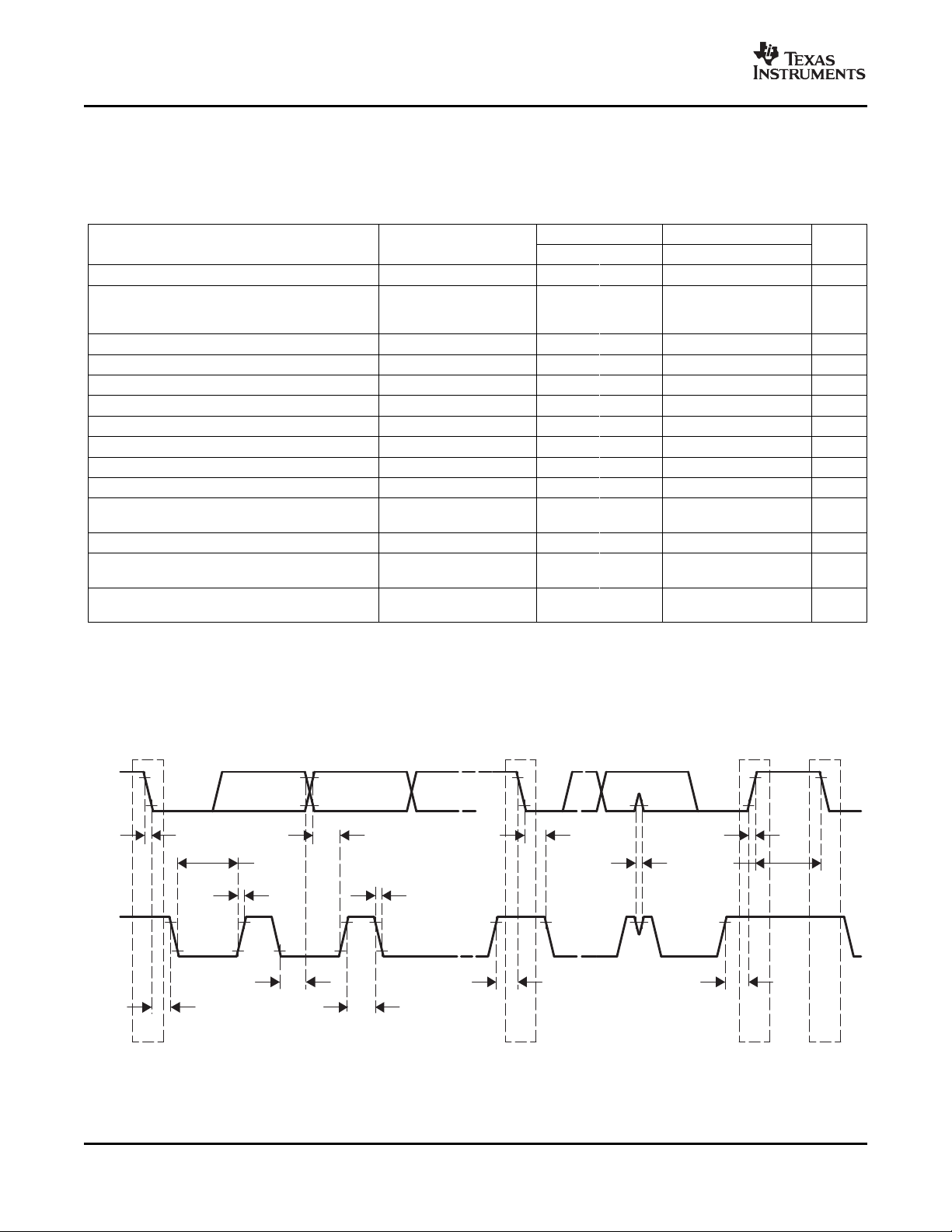
Serial Audio Port
t
h1
t
su1
t
su2
t
h2
SCLK
(Input)
LRCLK
(Input)
SDIN1
SDIN2
SDIN3
T0026-01
Serial audio port slave mode over recommended operating conditions (unless otherwise noted)
PARAMETER TEST CONDITIONS MIN TYP MAX UNIT
f
SCLK input frequency CL= 30 pF, SCLK = 64 f
SCLKIN
t
Setup time, LRCLK to SCLK rising edge 10 ns
su1
t
Hold time, LRCLK from SCLK rising edge 10 ns
h1
t
Setup time, SDIN to SCLK rising edge 10 ns
su2
t
Hold time, SDIN from SCLK rising edge 10 ns
h2
LRCLK frequency 32 48 192 kHz
SCLK duty cycle 40% 50% 60%
LRCLK duty cycle 40% 50% 60%
SCLK rising edges between LRCLK rising edges 64 64
LRCLK clock edge with respect to the falling edge of SCLK
SCLK period
TAS5086
SLES131B – FEBRUARY 2005 – REVISED JUNE 2007
S
2.048 12.288 MHz
–1/4 1/4
SCLK
edges
Figure 2. Slave Mode Serial Data Interface Timing
TAS5086 Pin-Related Characteristics of the SDA and SCL I/O Stages for F/S-Mode I2C-Bus Devices
PARAMETER TEST CONDITIONS UNIT
V
V
V
V
t
of
t
SP
I
i
C
(1) Cb= capacitance of one bus line in pF. The output fall time is faster than the standard I2C specification.
LOW-level input voltage –0.5 0.3 V
IL
HIGH-level input voltage 0.7 V
IH
Hysteresis of Schmitt-trigger inputs N/A N/A 0.05 V
hys
LOW-level output voltage (open drain or
OL1
open collector)
Output fall time from V
Pulse duration of spikes suppressed
to
IHmin
VILmax
3-mA sink current 0 0.4 V
Bus capacitance from 10 pF 7 + 0.1 C
to 400 pF
(2)
Input current, each I/O pin –30 30 –30
Capacitance, each I/O pin 10 10 pF
i
(2) SCL and SDA have a 30-ns glitch filter.
(3) The I/O pins of fast-mode devices must not obstruct the SDA and SDL lines if V
Submit Documentation Feedback
STANDARD MODE FAST MODE
MIN MAX MIN MAX
DD
250 250 ns
N/A N/A 0 30 ns
is switched off.
DD
DD
0.7 V
–0.5 0.3 V
DD
DD
b
(1)
(3)
V
DD
V
V
(3)
30
μ A
5
Page 6
www.ti.com
SDA
SCL
t
f
t
SU-DAT
t
HD-STA
t
r
t
BUF
t
SU-STO
P S
t
SP
t
SU-STA
Sr
t
HIGH
t
HD-DAT
t
LOW
t
r
t
HD-STA
S
t
f
T0114-01
TAS5086
SLES131B – FEBRUARY 2005 – REVISED JUNE 2007
TAS5086 Bus-Related Characteristics of the SDA and SCL I/O Stages for F/S-Mode I2C-Bus Devices
All values are referred to V
F/S-Mode I2C-Bus Devices ).
A
PARAMETER TEST CONDITIONS UNIT
f
SCL
t
HD-STA
t
LOW
t
HIGH
t
SU-STA
t
SU-DAT
t
HD-DAT
t
r
t
f
t
SU-STO
t
BUF
C
V
V
(1) Note that SDA does not have the standard I2C specification 300-ns hold time and that SDA must be valid by the rising and falling edges
(2) A fast-mode I2C-bus device can be used in a standard-mode I2C-bus system, but the requirement t
(3) Cb= total capacitance of one bus line in pF.
(4) Rise time varies with pullup resistor.
SCL clock frequency 0 100 0 400 kHz
Hold time (repeated) START condition.
After this period, the first clock pulse is 4 0.6 μ s
generated.
LOW period of the SCL clock 4.7 1.3 μ s
HIGH period of the SCL clock 4 0.6 μ s
Setup time for repeated START 4.7 0.6 μ s
Data setup time 250 100 μ s
Data hold time
(1) (2)
Rise time of both SDA and SCL 1000 7 + 0.1 C
Fall time of both SDA and SCL 300 7 + 0.1 C
Setup time for STOP condition 4 0.6 μ s
Bus free time between a STOP and 4.7 1.3 μ s
START condition
Capacitive loads for each bus line 400 400 pF
b
Noise margin at the LOW level for each
nL
connected device (including hysteresis)
Noise margin at the HIGH level for each
nH
connected device (including hysteresis)
of SCL. TI recommends that a 3.3-k Ω pullup resistor be used to avoid potential timing issues.
This is automatically the case if the device does not stretch the LOW period of the SCL signal. If such a device does stretch the LOW
period of the SCL signal, it must output the next data bit to the SDA line t
standard-mode I2C bus specification) before the SCL line is released.
and V
IHmin
(see TAS5086 Pin-Related Characteristics of the SDA and SCL I/O Stages for
ILmax
STANDARD MODE FAST MODE
MIN MAX MIN MAX
0 3.45 0 0.9 μ s
(3)
b
b
0.1 V
DD
0.2 V
DD
+ t
r-max
= 1000 + 250 = 1250 ns (according to the
SU-DAT
0.1 V
0.2 V
≥ 250 ns must then be met.
SU-DAT
500
(3)
DD
DD
(4)
300 ns
ns
V
V
Figure 3. Start and Stop Conditions Timing Waveforms
6
Submit Documentation Feedback
Page 7
www.ti.com
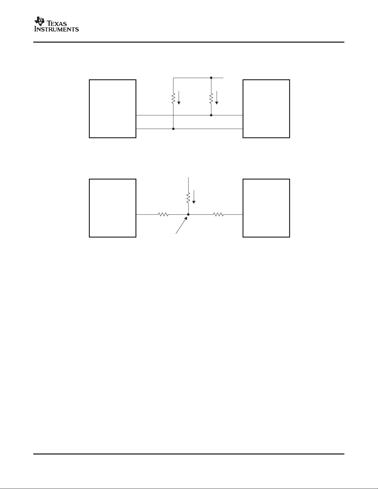
Recommended I2C Pullup Resistors
B0099-05
TAS5086
External
Microcontroller
V
I(SDA)
5V
I
P
I
P
V
I(SCL)
SDA
R
P
R
P
SCL
B0100-05
TAS5086 External
Microcontroller
V
I
5V
I
P
SDA
or
SCL
R
S
(2)
V
S
(1)
R
S
(2)
R
P
It is recommended that the I2C pullup resistors R
(see Figure 5 ), then the series resistor R
should be less than or equal to 300 Ω .
S
Figure 4. I2C Pullup Circuit (With No Series Resistor)
SLES131B – FEBRUARY 2005 – REVISED JUNE 2007
be 3.3 k Ω (see Figure 4 ). If a series resistor is in the circuit
P
TAS5086
(1) VS= 5 × RS/(R
+ RP). When driven low, VS<< VILrequirements.
S
(2) RS≤ 300 Ω
Figure 5. I2C Pullup Circuit (With Series Resistor)
Submit Documentation Feedback
7
Page 8
www.ti.com
1
2
3
4
5
6
7
8
9
10
11
12
13
14
15
16
17
18
19
38
37
36
35
34
33
32
31
30
29
28
27
26
25
24
23
22
21
20
VR_ANA
AVDD
AVSS
AVSS
PLL_FLTM
PLL_FLTP
AVSS
MCLK
RESET
PDN
DVDD
DVSS
DVSS_OSC
OSC_RES
VR_OSC
MUTE
SDA
SCL
LRCLK
PWM_1
PWM_2
PWM_3
PWM_4
PWM_5
PWM_6
VALID2
VALID1
VR_DIG
DVSS
DVSS
BKND_ERR
SDIN1
SDIN2
SDIN3
SDIN4
SDOUT
RESERVED
SCLK
DBT PACKAGE
(TOP VIEW)
P0034-01
TAS5086
SLES131B – FEBRUARY 2005 – REVISED JUNE 2007
PHYSICAL CHARACTERISTICS
Table 1. TERMINAL FUNCTIONS
TERMINAL
NAME NO.
AVDD 2 P 3.3-V analog power supply
AVSS P Analog supply ground
BKND_ERR 27 DI Pullup LOW to this terminal. BKND_ERR results in no change to any system
DVDD 11 P 3.3-V digital power supply
DVSS 28, P Digital ground
DVSS_OSC 13 P Digital ground for oscillator
LRCLK 19 DI 5-V Pulldown Input serial audio data left/right clock (sampling rate clock)
MCLK 8 DI 5-V Pulldown
MUTE 16 DI 5-V Pullup
OSC_RES 14 AO Oscillator trim resistor
(1) TYPE: A = analog; D = 3.3-V digital; P = power/ground/decoupling; I = input; O = output
(2) All pullups are 20- μ A weak pullups, and all pulldowns are 20- μ A weak pulldowns. The pullups and pulldowns are included to ensure
proper input logic levels if the terminals are left unconnected (pullups => logic 1 input; pulldowns => logic 0 input). Devices that drive
inputs with pullups must be able to sink 20 μ A while maintaining a logic-0 drive level. Devices that drive inputs with pulldowns must be
able to source 20 μ A while maintaining a logic-1 drive level.
8
3, 4,
7
12,
29
(1)
I/O
5-V
TOLERANT
TERMINATION
(2)
Submit Documentation Feedback
DESCRIPTION
Active-low. A back-end error sequence is generated by applying logic
parameters while VALID2 goes low.
MCLK is a 3.3-V clock master clock input. The input frequency of this
clock can range from 4 MHz to 50 MHz.
Performs a soft mute of outputs, active-low (muted signal = a logic low,
normal operation = a logic high). The mute control provides a noiseless
volume ramp to silence. Releasing mute provides a noiseless ramp to
previous volume.
Page 9
www.ti.com
SLES131B – FEBRUARY 2005 – REVISED JUNE 2007
PHYSICAL CHARACTERISTICS (continued)
Table 1. TERMINAL FUNCTIONS (continued)
TERMINAL
NAME NO.
PDN 10 DI 5-V Pullup
PLL_FLTM 5 AO PLL negative input
PLL_FLTP 6 AI PLL positive input
PWM_ 1 38 DO PWM 1 output
PWM_ 2 37 DO PWM 2 output
PWM_ 3 36 DO PWM 3 output
PWM_ 4 35 DO PWM 4 output
PWM_ 5 34 DO PWM 5 output
PWM_ 6 33 DO PWM 6 output
RESERVED 21 – RESERVED (connect to ground)
RESET 9 DI 5-V Pullup
SCL 18 DI 5-V I2C serial control clock input
SCLK 20 DI 5-V Pulldown
SDA 17 DIO 5-V I2C serial control data interface input/output
SDIN1 26 DI Pulldown
SDIN2 25 DI Pulldown
SDIN3 24 DI Pulldown
SDIN4 23 DI Pulldown
SDOUT 22 DI
VALID1 31 DO
VALID2 32 DO Output indicating validity of PWM outputs, active-high.
VR_ANA 1 P
VR_DIG 30 P
VR_OSC 15 P
(3) If desired, low-ESR capacitance values can be implemented by paralleling two or more ceramic capacitors of equal value. Paralleling
capacitors of equal value provides an extended high-frequency supply decoupling. This approach avoids the potential of producing
parallel resonance circuits that have been observed when paralleling capacitors of different values.
(1)
I/O
5-V
TOLERANT
TERMINATION
(2)
Power down, active-low. PDN powers down all logic, stops all clocks, and
performs a soft stop whenever a logic low is applied. The internal
parameters are preserved through a power-down cycle, as long as
RESET is not active. The duration for system recovery from power down
is 100 ms. When released, PDN powers up all logic, starts all clocks, and
performs a soft start that returns to the previous configuration.
A system reset is generated by applying a logic low to this terminal.
RESET is an asynchronous control signal that restores the TAS5086 to its
default conditions, sets the VALID2 output low, and places the PWM in
the hard-mute (M) state. Master volume is immediately set to full
attenuation. On the release of RESET, if PDN is high, the system
performs a 4–5-ms device initialization and sets the volume at mute.
Serial audio data clock (shift clock). SCLKIN is the serial audio port (SAP)
input data bit clock.
Serial audio data 1 input is one of the serial data input ports. SDIN1
supports four discrete (stereo) data formats.
Serial audio data 2 input is one of the serial data input ports. SDIN2
supports four discrete (stereo) data formats.
Serial audio data 3 input is one of the serial data input ports. SDIN3
supports four discrete (stereo) data formats.
Serial audio data 4 input is one of the serial data input ports. SDIN4
supports four discrete (stereo) data formats.
Serial audio data 1 output is the only serial data output port. SDOUT
supports I2S format only.
Soft start valid. Output indicating validity of soft-start PWM output,
active-high
Voltage reference for analog supply, 1.8 V. A pinout of the internally
regulated 1.8-V power. A 0.1- μ F, low-ESR capacitor should be connected
between this terminal and AVSS_PLL. This terminal must not be used to
power external devices.
Voltage reference for digital PWM core supply, 1.8 V. A pinout of the
internally regulated 1.8-V power used by digital PWM core logic. A 0.1- μ F,
low-ESR
DVSS_PWM. This terminal must not be used to power external devices.
Voltage reference for analog supply, 1.8 V. A pinout of the internally
regulated 1.8-V power. A 0.1- μ F, low-ESR
connected between this terminal and AVSS_PLL. This terminal must not
be used to power external devices.
(3)
capacitor should be connected between this terminal and
DESCRIPTION
(3)
capacitor should be
TAS5086
Submit Documentation Feedback
9
Page 10

www.ti.com
TAS5086
SLES131B – FEBRUARY 2005 – REVISED JUNE 2007
DETAILED DESCRIPTION
POWER SUPPLY
The TAS5086 power-supply section contains regulators that provide analog and digital regulated power for
various sections of the TAS5086. The analog supply supports the analog PLL while digital supplies support the
digital PLL, the digital audio processor, the pulse width modulator, and the output control (reclocker). The
power-supply section is enabled via VREG_EN.
CLOCK, ERROR RATE DETECTION, AND PLL
This module provides the timing and serial data interface for the TAS5086.
The TAS5086 is a clock slave device. It accepts MCLK, SCLK, and LRCLK.
The TAS5086 supports 64-f
The TAS5086 accepts a 64-f
192 fSand 384 fS.
TAS5086 checks to verify that SCLK is a specific value of 64 fSor 48 fS.
The TAS5086 supports a 1-f
The timing relationship of these clocks to SDIN[1:4] and SDOUT is shown in subsequent sections.
The clock section uses MCLK or the internal oscillator clock (when MCLK is unstable or absent) to produce
a 196-MHz PLL output.
The TAS5086 can auto-detect and set the internal clock control logic to the appropriate settings for the
frequencies of 32 kHz, normal speed (44.1 or 48 kHz), double speed (88.2 kHz or 96 kHz), and quad speed
(176.4 kHz or 192 kHz). The automatic sample rate detection can be disabled and the values set via I2C.
The TAS5086 also supports an AM interference-avoidance mode during which the clock rate is adjusted, in
concert with the PWM sample rate converter, to produce a PWM output at 7-f
The sample rate must be set manually during AM interference avoidance and when de-emphasis is enabled.
The TAS5086 uses an internal oscillator time base to provide reference timing information for the following
functions:
• MCLK, SCLK, and LRCLK error detection
• I2C communication when power is first applied to the device
• Automatic data-rate detection and setting (32 kHz, normal, double, and quad speed)
• Automatic MCLK rate detection and setting (64, 128, 192, 256, 384, and 512 fS)
MCLK for the 176.4-kHz and 192-kHz data rates.
S
SCLK rate for all MCLK ratios and a 48-f
S
LRCLK.
S
SCLK rate for MCLK ratios of
S
, 8-f
, or 9-f
S
S
.
S
OSCILLATOR TRIM
The TAS5086 PWM processor contains an internal oscillator for PLL reference. This reduces system cost
because an external reference is not required. After each power up or reset, a oscillator trim is needed; see the
Oscillator Trim Register (0x1B) section for a detailed procedure.
10
Submit Documentation Feedback
Page 11
www.ti.com
B0048-01
(L'+R')/2
Format
Channel
1–6
Channel
1–6
1–5
1–5
Down-
mix
SDIN1
PWM_1
PWM_2
PWM_3
PWM_4
PWM_5
PWM_6
1LF
2RF
3LS
4RS
5C
0x20
0x21
0x25
L'
R'
L'
R'
0x04
SDIN2
SDIN3
SDIN4
SDIN4
MUX
0x21
Ch-6Processing
MUX
MUX
Downmix
SDIN4
PWM
MUX
SDOUT
I S
2
0x07– 0x0D
0x03
VOL
SEL
VOL
VOL
VOL
VOL
MUX
TAS5086
SLES131B – FEBRUARY 2005 – REVISED JUNE 2007
DETAILED DESCRIPTION (continued)
SERIAL DATA INTERFACE
Serial data is input on SDIN1, SDIN2, SDIN3, and SDIN4. The PWM outputs and downmix are derived from
SDIN1, SDIN2, and SDIN3. SDIN4 is a selectable pass-through signal that is available at SDOUT as an I2S
output. The TAS5086 accepts 32-, 44.1-, 48-, 88.2-, 96-, 176.4-, and 192-kHz serial data in 16-, 20-, or 24-bit,
left-justified, right-justified, and I2S serial data formats.
Serial data is output on SDOUT. The SDOUT data format is I2S 24-bit at the same data rate as the input. The
SDOUT output is synchronized to use the SCLK and LRCLK signals. There is a 1- to 2.5-LRCLK frame delay
from the input data to the output data, depending on the input serial data format. The SDOUT output has no
I2C-controllable functions. It is always operational.
The parameters of this clock and serial data interface input format are I2C configurable.
I2C SERIAL CONTROL INTERFACE
The TAS5086 has an I2C serial control slave interface to receive commands from a system controller. The serial
control interface supports both normal-speed (100-kHz) and high-speed (400-kHz) operations without wait
states. As an added feature, this interface operates even if MCLK is absent.
The serial control interface supports both single-byte and multi-byte read and write operations for status
registers and the general control registers associated with the PWM.
The I2C interface supports a special mode that permits I2C write operations to be broken up into multiple-data
write operations that are multiples of 4 data bytes. These are 6-, 10-, 14-, 18-, ... etc., -byte write operations that
are composed of a device address, read/write bit, subaddress, and any multiple of 4 bytes of data. This permits
the system to write large register values incrementally without blocking other I2C transactions.
Figure 6 shows the data flow and control through the TAS5086. The major I2C registers are shown above each
applicable block (e.g., 0x04 is the serial data format control register).
Figure 6. TAS5086 Data Flow Diagram With I2C Registers
Submit Documentation Feedback
11
Page 12

www.ti.com
B0050-01
0x21
0x0D
BQ1(G)
0x23
Gain-
Compensated
Biquad
0x24
LowPass
Biquad
VOL
10dB
BassManagement
Ch1–5
Ch6Sub
FromDownmix(L’+R’)/2
S
BQ1 BQ2
MUX
TAS5086
SLES131B – FEBRUARY 2005 – REVISED JUNE 2007
DETAILED DESCRIPTION (continued)
Channel-6 Processing Section
Channel 6 has processing features that are directly applicable to the subwoofer channel.
Figure 7. Channel-6 Processing Block Diagram
PWM Section
The TAS5086 has six channels of high-performance digital PWM modulators that are designed to drive
switching output stages (back ends) in both single-ended (SE) and H-bridge (bridge-tied load) configurations.
The TAS5086 device uses noise-shaping and sophisticated error correction algorithms to achieve high power
efficiency and high-performance digital audio reproduction. The TAS5086 uses a fourth-order noise shaper to
provide >105-dB SNR performance from 20 Hz to 20 kHz.
The TAS5086 PWM interface is described by using the following notation:
PN + V
where
P = number of PWM signals per channel
N = number of channels
V = total number of valid signals used to reset the power stage
For example, the TAS5086 initial interface format means that there is 1 PWM signal per channel (N = 6) and 1
valid signal is used to reset the power stages. The shorthand notation to describe this is 1N+1.
The PWM section accepts 24-bit PCM data from the serial data interface and outputs six PWM audio output
channels to drive 1N+1 single-ended and BTL power stages.
The PWM interface supports:
• TAS5186 in BTL or SE mode without any external glue logic, uses 1N+1 signaling.
• TAS5142 in BTL or SE mode without any external glue logic, uses 1N+1 signaling.
• TAS5111 SE without any external glue logic, and with a pulldown on the output, uses 1N+1 signaling.
• TAS5111 BTL or TAS5112 BTL with one inverter per BTL channel of glue logic and a pulldown on the
output, uses 1N+1 signaling from TAS5086, 2N+1 input to TAS5111/12.
• TAS5112 SE (with external glue logic)
See the application schematics for an example of the TAS5086 with the TAS5186 and the TAS5086 with
TAS5112 SE and TAS5111 SE.
12
Submit Documentation Feedback
Page 13
www.ti.com
OutputStage
PSU
VPP
GND
IN
IN
VPP
GND
PWM
TAS5086
OUT
OUT
S0269-01
TAS5086
SLES131B – FEBRUARY 2005 – REVISED JUNE 2007
DETAILED DESCRIPTION (continued)
The TAS5086 has input multiplexers that allow any of the input channels to be routed to any PWM channel and
output multiplexers to enable any PWM output to be routed to any PWM output pin.
It also has individual channel dc-blocking filters that are enabled by default.
Individual channel de-emphasis filters for 32, 44.1, and 48 kHz are included and can be enabled and disabled.
There is also a two-channel downmix result that can be output on SDOUT (I2S format). This result also can be
sent to the left and right front channels (channels 1 and 2) and/or to the center and subwoofer (channels 5 and
6) as well.
A mixer on the subwoofer channel supports bass management configuration 1.
PWM output characteristics
• Up to 8 × oversampling
• 12 × at fS= 32 kHz, 8 × at fS= 48 kHz, 4 × at fS= 96 kHz, 2 × at fS= 192 kHz
• Fourth-order noise shaping
• ≥ 105-dB dynamic range, 0–20 kHz (TAS5086 + TAS5186 system measured at speaker terminals)
• THD < 0.06% (measured at TAS5086 outputs)
• Adjustable maximum modulation limit of 93.8% to 99.2%
Transitions Between Shutdown and Playing
The TAS5086 outputs are switching all the time with the noise shaper active. Mute is acheived by inputting a
zero into the noise shaper, with the noise shaper running and the output still switching. By using this approach,
the transitions between off and operation is avoided. The only exception is shutdown of surround channels as
described in the Surround Register (0x19) section.
Futhermore, the TAS5086 is designed to drive a load in single-ended and bridge-tied-load configurations. The
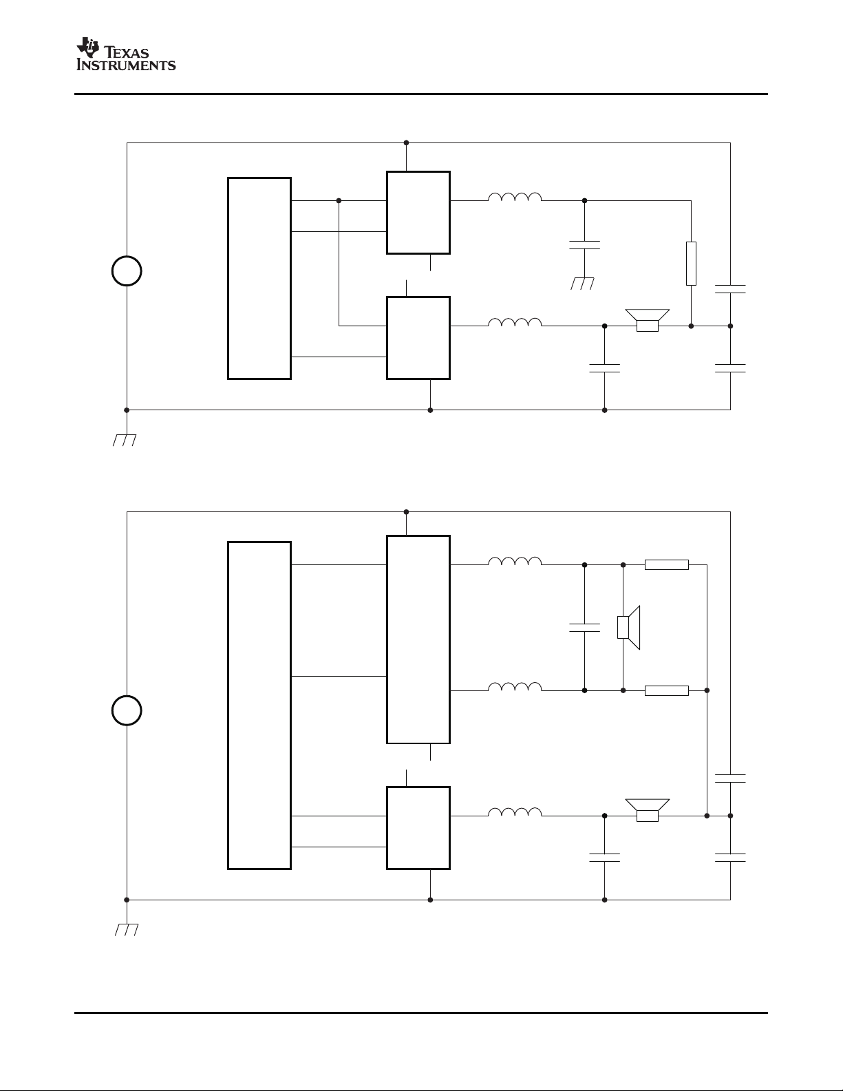
principle in the SE and BTL configurations is shown in Figure 8 and Figure 9 . In both situations, care must be
taken to ensure correct start-up sequences which charge the bootstrap capacitor and do not produce audible
artifacts; the TAS5086 is designed to do that.
Figure 8. BTL Filter Configuration
Submit Documentation Feedback
13
Page 14

www.ti.com
PSU
VPP
GND
INPWM
TAS5086
OUT
S0270-01
PowerStage
TAS5086
SLES131B – FEBRUARY 2005 – REVISED JUNE 2007
DETAILED DESCRIPTION (continued)
The SE configuration presents an additional challenge in order for starting up quietly. The second terminal of the
loudspeaker is connected to a split capacitor between power and ground. The advantage of this circuitly is that it
provides some degree of power-supply ripple rejection. The problem related to the split capacitor is that the
voltage over it must be controlled when the modulator starts (i.e., when the power stage output goes out of high
impedance state) to avoid a click in the speaker.
Figure 9. SE Filter Configuration
The TAS5086 supports two mechanisms for controlling the split-capacitor midpoint.
In the extra half-bridge scheme (the TAS5186 power stage is an example of this) an additional half-bridge is
started and brought to a 50-percent duty cycle, i.e., a situation where the average voltage of the half-bridge is
equal to the voltage which must be applied to the split-capacitor midpoint to start up without clicks in the
speaker. A resistor per channel is connected between the extra half-bridge and each midpoint for the split
capacitors. The split capacitors are charged through this resistor. This approach requires an extra VALID pin on
the modulator to control the extra half-bridge, therefore the 1N+2 interface. Figure 10 shows the topology of the
extra half-bridge. In some situations, a channel configured in BTL can be used to charge the split capacitor
instead of the extra half-bridge. This is shown in Figure 11 .
The mid-Z scheme charges the split capacitor through the loudspeaker. In order to do this without audible
artifacts the charge current must be limited. This is done by applying a start sequence which charges the output
state between low, high and high-Z. Because the ouput stage is in high-Z in a part of the sequence, the resulting
output impedance can be brought to a level suitable for charging the split capacitors without audible artifacts.
This solution does not require external components, as shown in Figure 9 . Not all power stages are compatible
with the mid-Z scheme, double-check the power-stage data sheet for compabitility. The PWM start register
(0x18) programs the TAS5086 for mid-Z or the standard low-Z start sequence.
14
Submit Documentation Feedback
Page 15
www.ti.com
S0271-01
PowerStage
ExtraHalf-Bridge
PSU
VPP
GND
IN
IN
VPP
GND
PWM
TAS5086
OUT
OUT
RES
RES
ValidSS
Valid
PowerStageSE
RES
ValidSS
Valid
PowerStageBTL
PSU
VPP
IN
RES
IN
VPP
GND
GND
PWM
PWM
TAS5086
OUT+
OUT–
OUT
S0272-01
DETAILED DESCRIPTION (continued)
TAS5086
SLES131B – FEBRUARY 2005 – REVISED JUNE 2007
Figure 10. Split-Capacitor Charging With Extra Half-Bridge
Submit Documentation Feedback
Figure 11. Split-Capacitor Charging With BTL Subwoofer
15
Page 16

www.ti.com
t
w(RESET)
Earliest time
that M-State
could be exited
RESET
M-State
t
r(DMSTATE)
< 200 ns
t
r(I2C_ready)
Start system
t
r(run)
Determine SCLK rate
and MCLK ratio. Enable via I2C.
T0029-03
PDN
M-State
t
su
t
p(DMSTATE)
< 1 ms
T0030-02
TAS5086
SLES131B – FEBRUARY 2005 – REVISED JUNE 2007
Reset Timing ( RESET)
Control-signal parameters over recommended operating conditions (unless otherwise noted)
PARAMETER MIN TYP MAX UNIT
t
r(DMSTATE)
t
w(RESET)
t
r(I2C_ready)
t
r(run)
NOTE: Because a crystal time base is used, the system determines the CLK rates. Once the data rate and master clock
Time to M-STATE low 370 ns
Pulse duration, RESET active 400 None ns
Time to enable I2C 3 ms
Device start-up time 10 ms
ratio are determined, the system outputs audio if a master volume command is issued.
Figure 12. Reset Timing
Power-Down ( PDN) Timing
Control-signal parameters over recommended operating conditions (unless otherwise noted). Note that PDN does not clear
I2C registers.
PARAMETER MIN TYP MAX UNIT
t
p(DMSTATE)
t
su
Time to M-STATE low 300 μ s
Number of MCLKs preceding the release of PDN 5
Device start-up time 120 ms
Figure 13. Power-Down Timing
16
Submit Documentation Feedback
Page 17

www.ti.com
BKND_ERR
M-State
or
Valid2
t
w(ER)
Normal
Operation
Normal
Operation
T0031-02
t
p(valid_low)
t
p(valid_high)
t
p(valid_high)
t
p(valid_low)
t
p(valid_low)
t
d(VOL)
VOLUME
MUTE
Normal
Operation
M-State
Normal
Operation
t
d(VOL)
T0032-01
SLES131B – FEBRUARY 2005 – REVISED JUNE 2007
Control-signal parameters over recommended operating conditions (unless otherwise noted). Note that PDN does not clear
I2C registers.
Back-End Error ( BKND_ERR)
Control-signal parameters over recommended operating conditions (unless otherwise noted)
PARAMETER MIN TYP MAX UNIT
t
w(ER)
t
p(valid_low)
t
p(valid_high)
Pulse duration, BKND_ERR active 350 None ns
<100 μ s
I2C programmable to be between 1 to 10 ms –25 25 % of interval
TAS5086
Figure 14. Error Recovery Timing
Mute Timing ( MUTE)
Control-signal parameters over recommended operating conditions (unless otherwise noted). Note that MUTE does not stop
PWM switching; it stops the noise shaper, and therefore has less noise.
PARAMETER MIN TYP MAX UNIT
t
Volume ramp time Defined by rate setting
d(VOL)
(1) See the Volume Control Register (0x0E) section.
(1)
Figure 15. Mute Timing
ms
Submit Documentation Feedback
17
Page 18

www.ti.com
23 22
SCLK
32 Clks
LRCLK (Note Reversed Phase) Left Channel
24-Bit Mode
9 8 5 4 1 0
19 18
20-Bit Mode
5 4 1 0
16-Bit Mode
1 015 14
MSB LSB
23 22
SCLK
32 Clks
Right Channel
9 8 5 4 1 0
19 18 5 4 1 0
1 015 14
MSB LSB
2-Channel I2S (Philips Format) Stereo Input/Output
T0034-04
TAS5086
SLES131B – FEBRUARY 2005 – REVISED JUNE 2007
SERIAL INTERFACE CONTROL AND TIMING
I2S TIMING
I2S timing uses LRCLK to define when the data being transmitted is for the left channel and when it is for the
right channel. LRCLK is low for the left channel and high for the right channel. A bit clock running at 64 fSis
used to clock in the data. A delay of one bit clock occurs from the time the LRCLK signal changes state to the
first bit of data on the data lines. The data is written MSB-first and is valid on the rising edge of the bit clock. The
TAS5086 masks unused trailing data bit positions.
18
Figure 16. I2S 64-f
Submit Documentation Feedback
Format
S
Page 19

www.ti.com
23 22
SCLK
24 Clks
LRCLK Left Channel
24-Bit Mode
1 0
19 18
20-Bit Mode
16-Bit Mode
15 14
MSB LSB
SCLK
24 Clks
Right Channel
MSB
2-Channel I2S (Philips Format) Stereo Input/Output (24-Bit Transfer Word Size)
T0092-01
3
25 49 817 16
1 04513 12
1 09 8
23 22 1
19 18
15 14
3
25 49 817 16
1 04513 12
1 09 8
LSB
SERIAL INTERFACE CONTROL AND TIMING (continued)
TAS5086
SLES131B – FEBRUARY 2005 – REVISED JUNE 2007
Figure 17. I2S 48-f
LEFT-JUSTIFIED
Left-justified (LJ) timing uses LRCLK to define when the data being transmitted is for the left channel and when
it is for the right channel. LRCLK is high for the left channel and low for the right channel. A bit clock running at
64 fSis used to clock in the data. The first bit of data appears on the data lines at the same time LRCLK toggles.
The data is written MSB-first and is valid on the rising edge of the bit clock. The TAS5086 masks unused trailing
data bit positions.
Format
S
Submit Documentation Feedback
19
Page 20

www.ti.com
23 22
SCLK
32 Clks
LRCLK
Left Channel
24-Bit Mode
9 8 5 4 1 0
MSB LSB
23 22
32 Clks
LRCLK
Right Channel
9 8 5 4 1 0
MSB LSB
18
20-Bit Mode
5 4 1 019
14
16-Bit Mode
1 015
18 5 4 1 019
14 1 015
2-Channel Left-Justified Stereo Input
T0034-02
23 22
SCLK
24 Clks
LRCLK
Left Channel
24-Bit Mode
1
19 18
20-Bit Mode
16-Bit Mode
15 14
MSB LSB
SCLK
24 Clks
Right Channel
MSB
2-Channel Left-Justified Stereo Input (24-Bit Transfer Word Size)
T0092-02
4
59 817 16
14513 12
19 8
0
0
0
21
17
13
23
22 1
19 18
15 14
4
59 817 16
14513 12
19 8
0
0
0
21
17
13
LSB
TAS5086
SLES131B – FEBRUARY 2005 – REVISED JUNE 2007
SERIAL INTERFACE CONTROL AND TIMING (continued)
Figure 18. Left-Justified 64-f
Format
S
20
Figure 19. Left-Justified 48-f
Submit Documentation Feedback
Format
S
Page 21

www.ti.com
23 22
SCLK
32 Clks
LRCLK
Left Channel
24-Bit Mode
19 18 15 14 1 0
19 18
20-Bit Mode
15 14 1 0
16-Bit Mode
1 015 14
MSB LSB
2-Channel Right-Justified (Sony Format) Stereo Input
23 22
32 Clks
Right Channel
19 18 15 14 1 0
19 18 15 14 1 0
1 015 14
MSB LSB
T0034-03
TAS5086
SLES131B – FEBRUARY 2005 – REVISED JUNE 2007
SERIAL INTERFACE CONTROL AND TIMING (continued)
Right-Justified
Right-justified (RJ) timing uses LRCLK to define when the data being transmitted is for the left channel and
when it is for the right channel. LRCLK is high for the left channel and low for the right channel. A bit clock
running at 64 fSis used to clock in the data. The first bit of data appears on the data 8 bit-clock periods (for
24-bit data) after LRCLK toggles. In RJ mode, the LSB of data always is clocked by the last bit clock before
LRCLK transitions. The data is written MSB-first and is valid on the rising edge of bit clock. The TAS5086 masks
unused leading data bit positions.
Figure 20. Right-Justified 64-f
Format
S
Submit Documentation Feedback
21
Page 22

www.ti.com
23 22
SCLK
24 Clks
LRCLK
Left Channel
24-Bit Mode
1
20-Bit Mode
16-Bit Mode
15 14
MSB LSB
SCLK
24 Clks
Right Channel
MSB
2-Channel Left-Justified Stereo Input (24-Bit Transfer Word Size)
T0092-03
5
19 18
1519 18
15
0
0
0
2
2
2
6
6
6
15 14
15 14
23 22 1
15 14
5
19 18
1519 18
15
0
0
0
2
2
2
6
6
6
15 14
15 14
LSB
TAS5086
SLES131B – FEBRUARY 2005 – REVISED JUNE 2007
SERIAL INTERFACE CONTROL AND TIMING (continued)
Figure 21. Right-Justified 48-f
I2C SERIAL CONTROL INTERFACE
The TAS5086 has a bidirectional Inter IC (I2C) interface that is compatible with the I2C bus protocol and
supports both single- and multiple-byte write and read operations. The control interface is used to program the
registers of the device and to read device status.
The TAS5086 supports wait-state insertions by other I2C devices on the bus. However, the TAS5086 performs
all I2C operations without I2C wait cycles.
The TAS5086 supports standard-mode I2C bus operation (100 kHz maximum) and fast I2C bus operation (400
kHz maximum).
GENERAL I2C OPERATION
The I2C bus employs two signals, SDA (data) and SCL (clock), to communicate between integrated circuits in a
system. Data is transferred on the bus serially, one bit at a time. The address and data are transferred in byte
(8-bit) format with the most-significant bit (MSB) transferred first. In addition, each byte transferred on the bus is
acknowledged by the receiving device with an acknowledge bit. Each transfer operation begins with the master
device driving a start condition on the bus and ends with the master device driving a stop condition on the bus.
The bus uses transitions on the data terminal (SDA) while the clock is high to indicate start and stop conditions.
A high-to-low transition on SDA indicates a start and a low-to-high transition indicates a stop. Normal data-bit
transitions must occur within the low time of the clock period. These conditions are shown in Figure 22 . The
master generates the 7-bit slave address and the read/write (R/ W) bit to open communication with another
device and then wait for an acknowledge condition. The TAS5086 holds SDA low during the acknowledge clock
period to indicate an acknowledgment. When this occurs, the master transmits the next byte of the sequence.
Each device is addressed by a unique 7-bit slave address plus R/ W bit (1 byte). All compatible devices share
the same signals via a bidirectional bus using a wired-AND connection. An external pullup resistor must be used
for the SDA and SCL signals to set the HIGH level for the bus.
22
Bit Format
S
Submit Documentation Feedback
Page 23

www.ti.com
7-BitSlave Address
R/
W
8-BitRegister Address(N)
A
8-BitRegisterDataFor
Address(N)
Start Stop
SDA
SCL
7
6
5
4
3
2 1
0
7
6
5
4
3
2 1
0
7
6
5
4
3
2 1
0
7
6
5
4
3
2 1
0
A
8-BitRegisterDataFor
Address(N)
A A
T0035-01
TAS5086
SLES131B – FEBRUARY 2005 – REVISED JUNE 2007
I2C SERIAL CONTROL INTERFACE (continued)
Figure 22. Typical I2C Sequence
An unlimited number of bytes can be transmitted between start and stop conditions. When the last word
transfers, the master generates a stop condition to release the bus. A generic data transfer sequence is shown
in Figure 22 .
The 7-bit address for the TAS5086 is 0011 011.
SINGLE- AND MULTIPLE-BYTE TRANSFERS
The serial control interface supports both single-byte and multiple-byte read/write operations for status registers
and the general control registers associated with the PWM. However, for the DAP data processing registers, the
serial control interface supports only multiple-byte (4-byte) read/write operations.
During multiple-byte read operations, the TAS5086 responds with data, a byte at a time, starting at the
subaddress assigned, as long as the master device continues to respond with acknowledges. If a particular
subaddress does not contain 32 bits, the unused bits are read as logic 0.
During multiple-byte write operations, the TAS5086 compares the number of bytes transmitted to the number of
bytes that are required for each specific subaddress. If a write command is received for a biquad subaddress,
the TAS5086 expects to receive five 32-bit words. If fewer than five 32-bit data words have been received when
a stop command (or another start command) is received, the data received is discarded. Similarly, if a write
command is received for a mixer coefficient, the TAS5086 expects to receive one 32-bit word.
Supplying a subaddress for each subaddress transaction is referred to as random I2C addressing. The TAS5086
also supports sequential I2C addressing. For write transactions, if a subaddress is issued, followed by data for
that subaddress and the 15 subaddresses that follow, a sequential I2C write transaction has taken place, and the
data for all 16 subaddresses is successfully received by the TAS5086. For I2C sequential write transactions, the
subaddress then serves as the start address and the amount of data subsequently transmitted, before a stop or
start is transmitted, determines how many subaddresses are written. As was true for random addressing,
sequential addressing requires that a complete set of data be transmitted. If only a partial set of data is written to
the last subaddress, the data for the last subaddress is discarded. However, all other data written is accepted;
just the incomplete data is discarded.
SINGLE-BYTE WRITE
As shown is Figure 23 , a single-byte data write transfer begins with the master device transmitting a start
condition, followed by the I2C device address and the read/write bit. The read/write bit determines the direction
of the data transfer. For a write data transfer, the read/write bit must be set to 0. After receiving the correct I2C
device address and the read/write bit, the TAS5086 device responds with an acknowledge bit. Next, the master
transmits the address byte or bytes corresponding to the TAS5086 internal memory address being accessed.
After receiving the address byte, the TAS5086 again responds with an acknowledge bit. Next, the master device
transmits the data byte to be written to the memory address being accessed. After receiving the data byte, the
TAS5086 again responds with an acknowledge bit. Finally, the master device transmits a stop condition to
complete the single-byte data write transfer.
Submit Documentation Feedback
23
Page 24

www.ti.com
A6 A5 A4 A3 A2 A1 A0
R/W
ACK A7 A6 A5 A4 A3 A2 A1 A0 ACK D7 D6 D5 D4 D3 D2 D1 D0 ACK
Start
Condition
Stop
Condition
Acknowledge Acknowledge Acknowledge
I CDevice Addressand
2
Read/WriteBit
Subaddress DataByte
T0036-01
D7 D0 ACK
Stop
Condition
Acknowledge
I CDevice Addressand
2
Read/WriteBit
Subaddress LastDataByte
A6 A5 A1 A0 R/W ACK A7 A5 A1 A0 ACK D7 ACK
Start
Condition
Acknowledge Acknowledge Acknowledge
FirstDataByte
A4 A3A6
OtherDataBytes
ACK
Acknowledge
D0 D7 D0
T0036-02
TAS5086
SLES131B – FEBRUARY 2005 – REVISED JUNE 2007
I2C SERIAL CONTROL INTERFACE (continued)
Figure 23. Single-Byte Write Transfer
MULTIPLE-BYTE WRITE AND INCREMENTAL MULTIPLE-BYTE WRITE
A multiple-byte data write transfer is identical to a single-byte data write transfer, except that multiple data bytes
are transmitted by the master device to TAS5086 as shown in Figure 24 . After receiving each data byte, the
TAS5086 responds with an acknowledge bit.
Figure 24. Multiple-Byte Write Transfer
The I2C supports a special mode that permits I2C write operations to be broken up into multiple data write
operations that are multiples of 4 data bytes. These are 6-, 10-, 14-, 18-, ..., etc., -byte write operations that are
composed of a device address, read/write bit, and subaddress and any multiple of 4 bytes of data. This permits
the system to write large register values incrementally without blocking other I2C transactions.
This feature is enabled by the append subaddress (0xFE) in the TAS5086. The append address, 0xFE, enables
the TAS5086 to append an integer number of 4-, 8-, 12-, 16-, … byte blocks of data to a register that was
opened by a previous I2C register write operation, but has not received its complete number of data bytes.
When the correct number of bytes has been received, the TAS5086 starts processing the data.
The procedure to perform a multiple-byte write operation is as follows.
1. Start a normal I2C write operation by sending the device address, write bit, register subaddress, and an
integer number of 4-byte data blocks. At the end of that sequence, a stop condition is sent.
At this point the register has been opened. It then accepts the remaining data sent by one or more write
operations, consisting of an integer number of 4-byte blocks. This data should be written to the append
subaddress (0xFE).
2. At a later time, one or more append data transfers are performed to incrementally transfer the remaining
number of bytes in sequential order to complete the register write operation. Each of these append
operations is composed of the device address, write bit, append subaddress (0xFE), and an integer
number of four bytes of data, followed by a stop condition.
3. The operation is terminated due to an error condition, and the data is flushed:
– If a new subaddress is written to the TAS5086 before the correct number of bytes has been written
– If a noninteger number of 4 bytes is written at the beginning or during any of the append operations
– If a read bit is sent
SINGLE-BYTE READ
As shown in Figure 25 , a single-byte data read transfer begins with the master device transmitting a start
condition, followed by the I2C device address and the read/write bit. For the data read transfer, both a write
24
Submit Documentation Feedback
Page 25

www.ti.com
A6 A5 A0 R/W ACK A7 A6 A5 A4 A0 ACK A6 A5 A0 ACK
Start
Condition
Stop
Condition
Acknowledge Acknowledge Acknowledge
I CDevice Addressand
2
Read/WriteBit
Subaddress DataByte
D7 D6 D1 D0 ACK
I CDevice Addressand
Read/WriteBit
2
Not
Acknowledge
R/WA1 A1
RepeatStart
Condition
T0036-03
A6 A0 ACK
Acknowledge
I CDevice Addressand
Read/WriteBit
2
R/WA6 A0 R/W ACK A0 ACK D7 D0 ACK
Start
Condition
Stop
Condition
Acknowledge Acknowledge Acknowledge
LastDataByte
ACK
FirstDataByte
RepeatStart
Condition
Not
Acknowledge
I CDevice Addressand
Read/WriteBit
2
Subaddress OtherDataBytes
A7 A6 A5 D7 D0 ACK
Acknowledge
D7 D0
T0036-04
TAS5086
SLES131B – FEBRUARY 2005 – REVISED JUNE 2007
I2C SERIAL CONTROL INTERFACE (continued)
followed by a read are actually done. Initially, a write is done to transfer the address byte or bytes of the internal
memory address to be read. As a result, the read/write bit is set to a 0. After receiving the TAS5086 address
and the read/write bit, the TAS5086 responds with an acknowledge bit. In addition, after sending the internal
memory address byte or bytes, the master device transmits another start condition, followed by the TAS5086
address and the read/write bit again. This time, the read/write bit is set to 1, indicating a read transfer. After
receiving the TAS5086 and the read/write bit, the TAS5086 again responds with an acknowledge bit. Next, the
TAS5086 transmits the data byte from the memory address being read. After receiving the data byte, the master
device transmits a not-acknowledge, followed by a stop condition, to complete the single-byte data read transfer.
Figure 25. Single-Byte Read Transfer
MULTIPLE-BYTE READ
A multiple-byte data read transfer is identical to a single-byte data read transfer, except that multiple data bytes
are transmitted by the TAS5086 to the master device as shown in Figure 26 . Except for the last data byte, the
master device responds with an acknowledge bit after receiving each data byte.
Figure 26. Multiple-Byte Read Transfer
COMMAND CHARACTERISTICS
The TAS5086 has two groups of I2C commands. One set is commands that are designed specifically to be
operated while audio is streaming and that have built-in mechanisms to prevent noise, clicks, and pops. The
other set does not have this built-in protection.
Commands that are designed to be adjusted while audio is streaming
• Master volume
• Master mute
• Individual channel volume
• Individual channel mute
Commands that the system executes without additional processing to prevent noise, clicks, or pops (in
a number of cases this does not produce an audible click and pop)
• Serial data interface format
• De-emphasis
• Sample rate conversion
• Input multiplexer
• Output multiplexer
Submit Documentation Feedback
25
Page 26

www.ti.com
TAS5086
SLES131B – FEBRUARY 2005 – REVISED JUNE 2007
I2C SERIAL CONTROL INTERFACE (continued)
• Biquads
• Downmix
• Channel delay
• Enable/disable automatic MCLK and data-rate detection
• Manual or automatic MCLK and data-rate setting
• Enable/disable dc blocking
• Hard/soft unmute from clock error
SERIAL CONTROL INTERFACE REGISTER SUMMARY
SUBADDRESS REGISTER NAME CONTENTS INITIALIZATION VALUE
0x00 Clock control register 1 Description shown in subsequent section 6C
0x01 Device ID register 1 Description shown in subsequent section 03
0x02 Error status register 1 Description shown in subsequent section 00
0x03 System control register 1 1 Description shown in subsequent section A0
0x04 Serial data interface register 1 Description shown in subsequent section 05
0x05 System control register 2 1 Description shown in subsequent section 60
0x06 Soft mute register 1 Description shown in subsequent section 00
0x07 Master volume 1 Description shown in subsequent section FF (mute)
0x08 Channel 1 vol 1 Description shown in subsequent section 30 (0 dB)
0x09 Channel 2 vol 1 Description shown in subsequent section 30 (0 dB)
0x0A Channel 3 vol 1 Description shown in subsequent section 30 (0 dB)
0x0B Channel 4 vol 1 Description shown in subsequent section 30 (0 dB)
0x0C Channel 5 vol 1 Description shown in subsequent section 30 (0 dB)
0x0D Channel 6 vol 1 Description shown in subsequent section 30 (0 dB)
0x0E Volume control register 1 Description shown in subsequent section B1
0x0F RESERVED
0x10 Modulation limit register 1 Description shown in subsequent section 02
0x11–0x17 RESERVED
0x18 PWM start register 1 Description shown in subsequent section 3F
0x19 Surround register 1 Description shown in subsequent section 00
0x1A Split cap charge period register 1 Description shown in subsequent section 18
0x1B OSC_TRIM 1 Oscillator trim register 82
0x1C BKNDERR register 1 BKNDErr Register 05
0x1D–0x1F RESERVED
0x20 Input MUX register 4 Description shown in subsequent section 0x00, 0x01, 0x23, 0x45
0x21 Downmix input MUX register 4 Description shown in subsequent section 0x00, 0x00, 0x00, 0x3F
0x22 AM tuned frequency 4 Description shown in subsequent section 0x00, 0x00, 0x00, 0x00
0x23 ch6_bq[1] 20 b0[25:24] b0[(23:16], b0[15:8], b0[7:0] 0x00, 0x80, 0x00, 0x00
0x24 ch6_bq[2] 20 b0[25:24] b0[23:16], b0[15:8], b0[7:0] 0x00, 0x80, 0x00, 0x00
NO. OF
BYTES
(1)
(1)
(1)
b1[25:24] b1[23:16], b1[15:8], b1[7:0] 0x00, 0x00, 0x00, 0x00
b2[25:24] b2[23:16], b2[15:8], b2[7:0] 0x00, 0x00, 0x00, 0x00
a1[25:24] a1[23:16], a1[15:8], a1[7:0] 0x00, 0x00, 0x00, 0x00
a2[25:24] a2[23:16], a2[15:8], a2[7:0] 0x00, 0x00, 0x00, 0x00
b1[25:24] b1[23:16], b1[15:8], b1[7:0] 0x00, 0x00, 0x00, 0x00
b2[25:24] b2[23:16], b2[15:8], b2[7:0] 0x00, 0x00, 0x00, 0x00
(1) Reserved registers should not be accessed.
26
Submit Documentation Feedback
Page 27

www.ti.com
TAS5086
SLES131B – FEBRUARY 2005 – REVISED JUNE 2007
SERIAL CONTROL INTERFACE REGISTER SUMMARY (continued)
SUBADDRESS REGISTER NAME CONTENTS INITIALIZATION VALUE
0x25 PWM MUX register Description shown in subsequent section 0x00, 0x32, 0x45, 0x10
0x26 1/G register 4 x[25:24] x[23:16], x[15:8], x[7:0] 0x00, 0x80, 0x00, 0x00
0x27 RESERVED
0x28 Scale register 4 x[25:24] x[23:16], x[15:8], x[7:0] 0x00, 0x80, 0x00, 0x00
0x29–0xFD RESERVED
0xFE Repeat subaddress 4+4N 0x00, 0x00, 0x00, 0x00
0xFF RESERVED
(2) Reserved registers should not be accessed.
CLOCK CONTROL REGISTER (0x00)
In the manual mode, the clock control register provides a way for the system microprocessor to update the data
and clock rates, based on the sample rate and associated clock frequencies. In the autodetect mode, the clocks
are determined automatically by the TAS5086. In this case, the clock control register contains the autodetected
clock status as automatically detected. Bits D7–D5 select the sample rate. Bits D4–D2 select the MCLK
frequency. Bit D1 selects the bit clock (SCLK) frequency. Bit D0 is used in manual mode only. In this mode,
when the clocks are updated, a 1 must be written to D1 to inform the TAS5086 that the written clocks are valid.
NO. OF
BYTES
a1[25:24] a1[23:16], a1[15:8], a1[7:0] 0x00, 0x00, 0x00, 0x00
a2[25:24] a2[23:16], a2[15:8], a2[7:0] 0x00, 0x00, 0x00, 0x00
(1)
(1)
(2)
Table 2. Clock Control Register (0x00)
D7 D6 D5 D4 D3 D2 D1 D0 FUNCTION
0 0 0 – – – – – fS= 32-kHz sample rate
0 0 1 – – – – – fS= 38-kHz sample rate
0 1 0 – – – – – fS= 44.1-kHz sample rate
0 1 1 – – – – – fS= 48-kHz sample rate
1 0 0 – – – – – fS= 88.2- kHz sample rate
1 0 1 – – – – – fS= 96-kHz sample rate
1 1 0 – – – – – fS= 176.4-kHz sample rate
1 1 1 – – – – – fS= 192-kHz sample rate
– – – 0 0 0 – – MCLK frequency = 64 × f
– – – 0 0 1 – – MCLK frequency = 128 × f
– – – 0 1 0 – – MCLK frequency = 192 × f
– – – 0 1 1 – – MCLK frequency = 256 × f
– – – 1 0 0 – – MCLK frequency = 384 × f
– – – 1 0 1 – – MCLK frequency = 512 × f
– – – 1 1 0 – – Reserved
– – – 1 1 1 – – Reserved
– – – – – – 1 – Bit clock (SCLK) frequency = 48 × f
– – – – – – 0 – Bit clock (SCLK) frequency = 64 × f
– – – – – – – 0 Clock not valid (in manual mode only)
– – – – – – – 1 Clock valid (in manual mode only)
(1) Default values are in bold
(2) MCLK frequency = 64 x fSis not available for 32-, 44.1-, 48-, 88.2-, and 96-kHz data rates
(2)
S
S
S
S
S
S
(1)
S
S
Submit Documentation Feedback
27
Page 28

www.ti.com
TAS5086
SLES131B – FEBRUARY 2005 – REVISED JUNE 2007
DEVICE ID REGISTER (0x01)
The device ID register contains the ID code for the TAS5086.
Table 3. General Status Register (0x01)
D7 D6 D5 D4 D3 D2 D1 D0 FUNCTION
0 Default
– 0 0 0 0 0 1 1 Identification code for the TAS5086
28
Submit Documentation Feedback
Page 29

www.ti.com
SLES131B – FEBRUARY 2005 – REVISED JUNE 2007
ERROR STATUS REGISTER (0x02)
Note that the error bits are sticky bits that are not cleared by the hardware. This means that the software must
clear the register (write zeroes) and then read them to determine if there are any persistent errors.
Table 4. Error Status Register (0x02)
D7 D6 D5 D4 D3 D2 D1 D0 FUNCTION
– 1 – – – – – – PLL auto lock error
– – 1 – – – – – SCLK error
– – – 1 – – – – LRCLK error
– – – – 1 – – – Frame slip
– 0 0 0 0 0 0 0 No errors
SYSTEM CONTROL REGISTER 1 (0x03)
System control register 1 has several functions:
Bit D7: If 0, the dc-blocking filter for each channel is disabled.
If 1, the dc-blocking filter (–3-dB cutoff < 1 Hz) for each channel is enabled (default).
Bit D6: Not used
Bit D5: If 0, use soft unmute on recovery from clock error. This is a slow recovery.
If 1, use hard unmute on recovery from clock error (default). This is a fast recovery.
Bit D4: If 0, the downmix is output on SDOUT as I2S signal (default).
If 1, SDIN4 is output on SDOUT as I2S signal.
Bit D3: If 0, clock autodetect is enabled (default).
If 1, clock autodetect is disabled.
Bit D2: If 0, soft start is enabled (default).
If 1, soft start is disabled.
Bits D1–D2: Select de-emphasis
TAS5086
Table 5. System Control Register 1 (0x03)
D7 D6 D5 D4 D3 D2 D1 D0 FUNCTION
0 – – – – – – – PWM high-pass (dc blocking) disabled
1 – – – – – – – PWM high-pass (dc blocking) enabled
– – 0 – – – – – Soft unmute on recovery from clock error
– – 1 – – – – – Hard unmute on recovery from clock error
– – – 0 – – – – Output downmix on SDOUT
– – – 1 – – – – Output SDIN4 mix on SDOUT
– – – – 0 – – – Enable clock autodetect
– – – – 1 – – – Disable clock autodetect
– – – – – 0 – – Enable soft start
– – – – – 1 – – Disable soft start
– – – – – – 0 0 No de-emphasis
– – – – – – 0 1 De-emphasis for fS= 32 kHz
– – – – – – 1 0 De-emphasis for fS= 44.1 kHz
– – – – – – 1 1 De-emphasis for fS= 48 kHz
Submit Documentation Feedback
29
Page 30

www.ti.com
TAS5086
SLES131B – FEBRUARY 2005 – REVISED JUNE 2007
SERIAL DATA INTERFACE REGISTER (0x04)
As shown in Table 6 , the TAS5086 supports nine serial data modes. The default is 24-bit, I2S mode.
Table 6. Serial Data Interface Control Register (0x04) Format
RECEIVE SERIAL DATA WORD D7–D4 D3 D2 D1 D0
INTERFACE FORMAT LENGTHS
Right-justified 16 0000 0 0 0 0
Right-justified 20 0000 0 0 0 1
Right-justified 24 0000 0 0 1 0
I2S 16 0000 0 0 1 1
I2S 20 0000 0 1 0 0
I2S 24 0000 0 1 0 1
Left-justified 16 0000 0 1 1 0
Left-justified 20 0000 0 1 1 1
Left-justified 24 0000 1 0 0 0
Reserved 0000 1 0 0 1
Reserved 0000 1 0 1 0
Reserved 0000 1 0 1 1
Reserved 0000 1 1 0 0
Reserved 0000 1 1 0 1
Reserved 0000 1 1 1 0
Reserved 0000 1 1 1 1
Default values are in bold
SYSTEM CONTROL REGISTER 2 (0x05)
Bit D6 is a control bit and bit D5 is a configuration bit.
When bit D6 is set low, the system starts playing; otherwise, the outputs are shut down.
Bit D5 defines the configuration of the system, i.e., it determines what configuration the system runs in when bit
D6 is set low. When this bit is asserted, the system is configured to surround, meaning all channels are
switching. Otherwise, only a subset of the PWMs runs, corresponding to a 2.0 or 2.1 configuration as
determined by the surround register (0x19).
Bit D5 should be changed only when bit D6 is set to 1, meaning that it is only possible to switch configuration
from surround to 2.0/2.1 by resetting the TAS5086 and then restarting it again in the new configuration.
Table 7. System Control Register 2 (0x05)
D7 D6 D5 D4 D3 D2 D1 D0 FUNCTION
– 1 X – – – – – All channels are shut down (hard mute).
– 1 1 – – – – – All channels are shut down (hard mute). VALID1 = 0 and VALID2 = 0
– 0 1 – – – – – When D6 is deasserted, all channels are started. VALID1 = 1 and VALID2 = 1
– 0 0 – – – – – When D6 is deasserted, all channels not belonging to shutdown group 1 are
started. VALID1 = 0 and VALID2 = 1
30
Submit Documentation Feedback
Page 31

www.ti.com
SOFT MUTE REGISTER (0x06)
Table 8. Soft Mute Register (0x06)
D7 D6 D5 D4 D3 D2 D1 D0 FUNCTION
– – – – – – – 1 Soft mute channel 1
– – – – – – 1 – Soft mute channel 2
– – – – – 1 – – Soft mute channel 3
– – – – 1 – – – Soft mute channel 4
– – – 1 – – – – Soft mute channel 5
– – 1 – – – – – Soft mute channel 6
0 0 0 0 0 0 0 0 Unmute all channels
VOLUME REGISTERS (0x07, 0x08, 0x09, 0x0A, 0x0B, 0x0C, 0x0D)
Master volume – 0x07 (default is mute)
Channel 1 volume – 0x08 (default is 0 dB)
Channel 2 volume – 0x09 (default is 0 dB)
Channel 3 volume – 0x0A (default is 0 dB)
Channel 4 volume – 0x0B (default is 0 dB)
Channel 5 volume – 0x0C (default is 0 dB)
Channel 6 volume – 0x0D (default is 0 dB)
TAS5086
SLES131B – FEBRUARY 2005 – REVISED JUNE 2007
Table 9. Volume Register
D7 D6 D5 D4 D3 D2 D1 D0 FUNCTION
0 0 0 0 0 0 0 0 24 dB
0 0 1 1 0 0 0 0 0 dB (default for individual channel volume)
1 1 1 1 1 1 1 0 –103 dB
1 1 1 1 1 1 1 1 MUTE (default for master volume)
Submit Documentation Feedback
31
Page 32

www.ti.com
TAS5086
SLES131B – FEBRUARY 2005 – REVISED JUNE 2007
VOLUME CONTROL REGISTER (0x0E)
Bit D7: Reserved = 1
Bit D6: If 0, then biquad 1 (BQ1) volume compensation part only is disabled (default).
If 1, then BQ1 volume compensation is enabled.
Bit D5: If 0, disable 38-kHz detection (38 kHz should be set manually by the microprocessor).
If 1, enable 38-kHz detection.
Bit D4: Reserved = 1
Bit D3: Not used
Bits D2–D0: Volume slew rate
Table 10. Volume Control Register (0x0E)
D7 D6 D5 D4 D3 D2 D1 D0 FUNCTION
1 – – – – – – – Reserved (must be 1)
– 0 – – – – – – Disable biquad volume compensation
– 1 – – – – – – Enable biquad volume compensation
– – 1 – – – – – Reserved = 1
– – – 1 – – – – Reserved (must be 1)
MODULATION LIMIT REGISTER (0x10)
Set modulation limit. See the appropriate power stage data sheet for recommended modulation limits.
Table 11. Modulation Limit Register (0x10)
D7 D6 D5 D4 D3 D2 D1 D0 LIMIT MIN WIDTH MODULATION
– – – – – 0 0 0 1 2 99.2%
– – – – – 0 0 1 2 4 98.4%
– – – – – 0 1 0 3 6 97.7%
– – – – – 0 1 1 4 8 96.9%
– – – – – 1 0 0 5 10 96.1%
– – – – – 1 0 1 6 12 95.3%
– – – – – 1 1 0 7 14 94.5%
– – – – – 1 1 1 8 16 93.8%
[DCLKs] [DCLKs] LIMIT
32
Submit Documentation Feedback
Page 33

www.ti.com
TAS5086
SLES131B – FEBRUARY 2005 – REVISED JUNE 2007
PWM START REGISTER (0x18)
Bits D7 and D6: Define which start sequence is used, either low-Z or mid-Z. Not all power stages are compatible
with mid-Z; double-check the power-stage data sheet.
Bits D5–D0: Define which PWMs are used for charging the split capacitors and which PWMs should stay low,
indicating the output stages are to be held in Hi-Z under split-capacitor charging.
For most systems, this register is always 0x3F. The setting depends on how the power stage is connected.
Table 12. PWM Start Register (0x18)
D7 D6 D5 D4 D3 D2 D1 D0 FUNCTION
0 – – – – – – – Use Low-Z sequence for part 1 of the start
1 – – – – – – – Use Mid-Z sequence for part 1 of the start
– 0 – – – – – – Use Low-Z sequence for part 2 of the start
– 1 – – – – – – Use Mid-Z sequence for part 2 of the start
– – 1 – – – – – Start channel 6 under part 1 of the start
– – 0 – – – – – Start channel 6 under part 2 of the start
– – – 1 – – – – Start channel 5 under part 1 of the start
– – – 0 – – – – Start channel 5 under part 2 of the start
– – – – 1 – – – Start channel 4 under part 1 of the start
– – – – 0 – – – Start channel 4 under part 2 of the start
– – – – – 1 – – Start channel 3 under part 1 of the start
– – – – – 0 – – Start channel 3 under part 2 of the start
– – – – – – 1 – Start channel 2 under part 1 of the start
– – – – – – 0 – Start channel 2 under part 2 of the start
– – – – – – – 1 Start channel 1 under part 1 of the start
– – – – – – – 0 Start channel 1 under part 2 of the start
Submit Documentation Feedback
33
Page 34

www.ti.com
TAS5086
SLES131B – FEBRUARY 2005 – REVISED JUNE 2007
SURROUND REGISTER (0x19)
Defines which channels should be running in the 2.0/2.1 mode.
The channels having their surround register set (HIGH) belong to shutdown group 1. They are associated with
VALID1. VALID1 is the signal that is driven low to disable channels when the system is operating in, for
example, stereo mode or 2.1 mode.
Example: If
PWM_1 connects to front left
PWM_2 connects to front right
PWM_3 connects to surround left
PWM_4 connects to surround right
PWM_5 connects to center
PWM_6 connects to sub
and you have a 2.1 mode, then VALID1 connects to the reset of surround left, surround right, and center.
VALID2 connects to the reset of front left, front right, and sub.
That means that the surround register (0x19) is loaded with 0001 1100b = 0x1C.
Important note: You must always change channel modes with all channels shut down (register 0x05 =
60).
Table 13. Surround Register (0x19)
D7 D6 D5 D4 D3 D2 D1 D0 FUNCTION
– – 1 – – – – – PWM_6 belongs to shutdown group 1 (VALID1)
– – 0 – – – – – PWM_6 belongs to shutdown group 2 (VALID2)
– – – 1 – – – – PWM_5 belongs to shutdown group 1 (VALID1)
– – – 0 – – – – PWM_5 belongs to shutdown group 2 (VALID2)
– – – – 1 – – – PWM_4 belongs to shutdown group 1 (VALID1)
– – – – 0 – – – PWM_4 belongs to shutdown group 2 (VALID2)
– – – – – 1 – – PWM_3 belongs to shutdown group 1 (VALID1)
– – – – – 0 – – PWM_3 belongs to shutdown group 2 (VALID2)
– – – – – – 1 – PWM_2 belongs to shutdown group 1 (VALID1)
– – – – – – 0 – PWM_2 belongs to shutdown group 2 (VALID2)
– – – – – – – 1 PWM_1 belongs to shutdown group 1 (VALID1)
– – – – – – – 0 PWM_1 belongs to shutdown group 2 (VALID2)
34
Submit Documentation Feedback
Page 35

www.ti.com
TAS5086
SLES131B – FEBRUARY 2005 – REVISED JUNE 2007
SPLIT-CAPACITOR CHARGE PERIOD REGISTER (0x1A)
This register should contain the code that closely matches the external single-ended split-capacitor charge
period. The TAS5086 waits for this period of time before starting the PWM signals. This helps reduce pops and
clicks. This is used only with the split-capacitor configuration.
Table 14. Split-Capacitor Charge Period Register (0x1A)
D7 D6 D5 D4 D3 D2 D1 D0 FUNCTION
– – – 0 0 – – – No split-capacitor charge period
– – – 0 1 0 0 0 13-ms split-capacitor charge period
– – – 0 1 0 0 1 16.9-ms split-capacitor charge period
– – – 0 1 0 1 0 23.4-ms split-capacitor charge period
– – – 0 1 0 1 1 31.2-ms split-capacitor charge period
– – – 0 1 1 0 0 41.6-ms split-capacitor charge period
– – – 0 1 1 0 1 54.6-ms split-capacitor charge period
– – – 0 1 1 1 0 72.8-ms split-capacitor charge period
– – – 0 1 1 1 1 96.2-ms split-capacitor charge period
– – – 1 0 0 0 0 130-ms split-capacitor charge period
– – – 1 0 0 0 1 156-ms split-capacitor charge period
– – – 1 0 0 1 0 234-ms split-capacitor charge period
– – – 1 0 0 1 1 312-ms split-capacitor charge period
– – – 1 0 1 0 0 416-ms split-capacitor charge period
– – – 1 0 1 0 1 546-ms split-capacitor charge period
– – – 1 0 1 1 0 728-ms split-capacitor charge period
– – – 1 0 1 1 1 962-ms split-capacitor charge period
– – – 1 1 0 0 0 1300-ms split-capacitor charge period
– – – 1 1 0 0 1 1690-ms split-capacitor charge period
– – – 1 1 0 1 0 2340-ms split-capacitor charge period
– – – 1 1 0 1 1 3120-ms split-capacitor charge period
– – – 1 1 1 0 0 4160-ms split-capacitor charge period
– – – 1 1 1 0 1 5460-ms split-capacitor charge period
– – – 1 1 1 1 0 7280-ms split-capacitor charge period
– – – 1 1 1 1 1 9620-ms split-capacitor charge period
Submit Documentation Feedback
35
Page 36

www.ti.com
TAS5086
SLES131B – FEBRUARY 2005 – REVISED JUNE 2007
OSCILLATOR TRIM REGISTER (0x1B)
The TAS5086 PWM processor contains an internal oscillator for PLL reference. This reduces system cost
because an external reference is not required. A trim resitor value of 18 k Ω is recomended. This should be
connected between TAS5086 pin 14 (OSC_RES) and pin 12 (DVSS).
Two procedures are available for trimming the internal oscillator. The factory-trim procedure is recommended for
most users. This procedure simply enables the factory trim that was previously done at the TAS5086 factory.
Note that only one trim procedure should be used. It always should be run following reset of the TAS5086.
Oscillator Factory-Trim Enable Procedure Example
1. Reset the TAS5086 (power up or toggle the RESET pin).
2. Write data 0x00 to register 0x1B (enable factory trim).
3. Write data 0x20 to register 0x05 (start all channels).
4. Write data 0x30 to register 0x07 (unmute and set master volume to 0 dB).
Oscillator Field-Trim Procedure Example (Use only if input LRCLK frequency is known)
1. Reset the TAS5086 (power up or toggle the RESET pin).
2. Provide a known LRCLK (e.g., 48 kHz).
3. Write LRCLK frequency to register 0x00 (e.g., for 48 kHz, write 0x6D to register 0x00).
4. Write data 0x03 to register 0x1B (field-trim command).
5. Write data 0x20 to register 0x05 (start all channels).
6. Write data 0x30 to register 0x07 (unmute and set master volume to 0 dB).
Table 15. Oscillator Trim Register (0x1B)
D7 D6 D5 D4 D3 D2 D1 D0 FUNCTION
– 0 – – – – – – Oscillator trim not done (read only)
– 1 – – – – – – Oscillator trim done
– – 0 0 0 0 – – Reserved
– – – – – – 0 – Select factory trim
– – – – – – 1 – Select field trim
– – – – – – – 1 Trim oscillator command
BKNDERR REGISTER (0x1C)
When a back-end error signal is received ( BKND_ERR = LOW), all the output stages are reset by setting all
PWM, VALID1, and VALID2 signals LOW. Subsequently, the modulator waits approximately for the time listed in
Table 16 before initiation of a reset.
Table 16. BKNDERR Register (0x1C)
D7 D6 D5 D4 D3 D2 D1 D0 FUNCTION
– – – – 0 0 0 0 Set back-end reset period to < 1.3 ms
– – – – 0 0 0 1 Set back-end reset period to 1.3 ms
– – – – 0 0 1 0 Set back-end reset period to 2.6 ms
– – – – 0 0 1 1 Set back-end reset period to 3.9 ms
– – – – 0 1 0 0 Set back-end reset period to 5.2 ms
– – – – 0 1 0 1 Set back-end reset period to 6.5 ms
– – – – 0 1 1 0 Set back-end reset period to 7.8 ms
– – – – 0 1 1 1 Set back-end reset period to 9.1 ms
– – – – 1 0 0 0 Set back-end reset period to 10.4 ms
– – – – 1 0 0 1 Set back-end reset period to 11.7 ms
– – – – 1 0 1 0 Set back-end reset period to 13 ms
36
Submit Documentation Feedback
Page 37

www.ti.com
SLES131B – FEBRUARY 2005 – REVISED JUNE 2007
Table 16. BKNDERR Register (0x1C) (continued)
D7 D6 D5 D4 D3 D2 D1 D0 FUNCTION
– – – – 1 0 1 1 Set back-end reset period to 13 ms
– – – – 1 1 X X Set back-end reset period to 13 ms
INPUT MULTIPLEXER REGISTER (0x20)
The hexadecimal value for each nibble is the channel number. For each input multiplexer, any input from SDIN1,
SDIN2, and SDIN3 can be mapped to any internal TAS5086 channel.
Default is 0x0001 2345.
Table 17. Input Multiplexer Register (0x20)
D31 D30 D29 D28 D27 D26 D25 D24 FUNCTION
0 0 0 0 0 0 0 0 Reserved = 0x00
D23 D22 D21 D20 D19 D18 D17 D16 FUNCTION
0 0 0 0 – – – – SDIN1-L to channel 1
0 0 0 1 – – – – SDIN1-R to channel 1
0 0 1 0 – – – – SDIN2-L to channel 1
0 0 1 1 – – – – SDIN2-R to channel 1
0 1 0 0 – – – – SDIN3-L to channel 1
0 1 0 1 – – – – SDIN3-R to channel 1
0 1 1 0 – – – – Ground (0) to channel 1
0 1 1 1 – – – – No connection
– – – – 0 0 0 0 SDIN1-L to channel 2
– – – – 0 0 0 1 SDIN1-R to channel 2
– – – – 0 0 1 0 SDIN2-L to channel 2
– – – – 0 0 1 1 SDIN2-R to channel 2
– – – – 0 1 0 0 SDIN3-L to channel 2
– – – – 0 1 0 1 SDIN3-R to channel 2
– – – – 0 1 1 0 Ground (0) to channel 2
– – – – 0 1 1 1 No connection
TAS5086
D15 D14 D13 D12 D11 D10 D9 D8 FUNCTION
0 0 0 0 – – – – SDIN1-L to channel 3
0 0 0 1 – – – – SDIN1-R to channel 3
0 0 1 0 – – – – SDIN2-L to channel 3
0 0 1 1 – – – – SDIN2-R to channel 3
0 1 0 0 – – – – SDIN3-L to channel 3
0 1 0 1 – – – – SDIN3-R to channel 3
0 1 1 0 – – – – Ground (0) to channel 3
0 1 1 1 – – – – No connection
– – – – 0 0 0 0 SDIN1-L to channel 4
– – – – 0 0 0 1 SDIN1-R to channel 4
– – – – 0 0 1 0 SDIN2-L to channel 4
– – – – 0 0 1 1 SDIN2-R to channel 4
– – – – 0 1 0 0 SDIN3-L to channel 4
– – – – 0 1 0 1 SDIN3-R to channel 4
– – – – 0 1 1 0 Ground (0) to channel 4
– – – – 0 1 1 1 No connection
Submit Documentation Feedback
37
Page 38

www.ti.com
TAS5086
SLES131B – FEBRUARY 2005 – REVISED JUNE 2007
Table 17. Input Multiplexer Register (0x20) (continued)
D7 D6 D5 D4 D3 D2 D1 D0 FUNCTION
0 0 0 0 – – – SDIN1-L to channel 5
0 0 0 1 – – – – SDIN1-R to channel 5
0 0 1 0 – – – SDIN2-L to channel 5
0 0 1 1 – – – SDIN2-R to channel 5
0 1 0 0 – – – SDIN3-L to channel 5
0 1 0 1 – – – – SDIN3-R to channel 5
0 1 1 0 – – – – Ground (0) to channel 5
0 1 1 1 – – – – No connection
– – – – 0 0 0 0 SDIN1-L to channel 6
– – – – 0 0 0 1 SDIN1-R to channel 6
– – – – 0 0 1 0 SDIN2-L to channel 6
– – – – 0 0 1 1 SDIN2-R to channel 6
– – – – 0 1 0 0 SDIN3-L to channel 6
– – – – 0 1 0 1 SDIN3-R to channel 6
– – – – 0 1 1 0 Ground (0) to channel 6
– – – – 0 1 1 1 No connection
38
Submit Documentation Feedback
Page 39

www.ti.com
SLES131B – FEBRUARY 2005 – REVISED JUNE 2007
DOWNMIX INPUT MULTIPLEXER REGISTER (0x21)
Bits D31–D16: Unused
Bits D15–D13: For this description, see Figure 6 .
Bit D12: If 1, selects downmix data L’ to TAS5086 internal channel 1
If 0, selects channel 1 data (from input multiplexer 1) to the TAS5086 internal channel 1
Bit D11: If 1, selects downmix data R’ to the TAS5086 internal channel 2
If 0, selects channel 2 data (from input multiplexer 2) to the TAS5086 internal channel 2
Bit D10: If 1, selects downmix data (L’+R’)/2 to the TAS5086 internal channel 5
If 0, selects channel 5 data (from input multiplexer 5) to the TAS5086 internal channel 5
Bits D9-D8: Selects either channel 6 data (from input multiplexer 6) or channel 6 data that has been
processed through bass management block or downmix data (L’+R’)/2 to the TAS5086
internal channel 6
Bits D7–D5: Unused.
Bit D4: If 1, enable data from input multiplexer 5 to downmix block
If 0, disable data from input multiplexer 5 to downmix block
Bit D3: If 1, enable data from input multiplexer 4 to downmix block
If 0, disable data from input multiplexer 4 to downmix block
Bit D2: If 1, enable data from input multiplexer 3 to downmix block
If 0, disable data from input multiplexer 3 to downmix block
Bit D1: If 1, enable data from input multiplexer 2 to downmix block
If 0, disable data from input multiplexer 2 to downmix block
Bit D0: If 1, enable data from input multiplexer 1 to downmix block
If 0, disable data from input multiplexer 1 to downmix block
TAS5086
Table 18. Downmix Input Multiplexer Register
D31 D30 D29 D28 D27 D26 D25 D24 FUNCTION
– – – – – – – – Unused
D23 D22 D21 D20 D19 D18 D17 D16 FUNCTION
– – – – – – – – Unused
D15 D14 D13 D12 D11 D10 D9 D8 FUNCTION
0 1 0 – – – – – RESERVED
– – – 1 – – – – Enable downmix data L’ to channel 1
– – – 0 – – – – Enable channel 1 data to channel 1
– – – – 1 – – – Enable downmix data R’ to channel 2
– – – – 0 – – – Enable channel 2 data to channel 2
– – – – – 1 – – Enable downmix data (L’+R’)/2 to channel 5
– – – – – 0 – – Enable channel 5 data to channel 5
– – – – – – 0 0 Enable channel 6 data to channel 6
– – – – – – 0 1 Bass management on channel 6
– – – – – – 1 x Enable downmix data (L’+R’)/2 to channel 6
D7 D6 D5 D4 D3 D2 D1 D0 FUNCTION
– – – – – – – 1 Enable data from input multiplexer 1 to downmix block
– – – – – – – 0 Disable data from input multiplexer 1 to downmix block
Submit Documentation Feedback
39
Page 40

www.ti.com
TAS5086
SLES131B – FEBRUARY 2005 – REVISED JUNE 2007
Table 18. Downmix Input Multiplexer Register (continued)
D31 D30 D29 D28 D27 D26 D25 D24 FUNCTION
– – – – – – – – Unused
– – – – – – 1 – Enable data from input multiplexer 2 to downmix block
– – – – – – 0 – Disable data from input multiplexer 2 to downmix block
– – – – – 1 – – Enable data from input multiplexer 3 to downmix block
– – – – – 0 – – Disable data from input multiplexer 3 to downmix block
– – – – 1 – – – Enable data from input multiplexer 4 to downmix block
– – – – 0 – – – Disable data from input multiplexer 4 to downmix block
– – – 1 – – – – Enable data from input multiplexer 5 to downmix block
– – – 0 – – – – Disable data from input multiplexer 5 to downmix block
AM Mode REGISTER (0x22)
See the PurePath Digital™ AM Interference Avoidance application report (SLEA040 ).
Table 19. AM Mode Register (0x22)
D20 D19 D18 D17 D16 FUNCTION
0 – – – – AM mode disabled
1 – – – – AM mode enabled
– 0 0 – – Select sequence 1
– 0 1 – – Select sequence 2
– 1 0 – – Select sequence 3
– 1 1 – – Select sequence 4
– – – 0 – IF frequency = 455 kHz
– – – 1 – IF frequency = 262.5 kHz
– – – – 0 Use BCD tuned frequency
– – – – 1 Use binary tuned frequency
Table 20. AM Tuned Frequency Register in BCD Mode
D15 D14 D13 D12 D11 D10 D9 D8 FUNCTION
0 0 0 X – – – – BCD frequency (1000s kHz)
– – – – – – – –
– – – – X X X X BCD frequency (100s kHz)
0 0 0 0 0 0 0 0 Default value
D7 D6 D5 D4 D3 D2 D1 D0 FUNCTION
X X X X – – – – BCD frequency (10s kHz)
– – – – – – – –
– – – – X X X X BCD frequency (1s kHz)
0 0 0 0 0 0 0 0 Default value
OR
Table 21. AM Tuned Frequency Register in Binary Mode
D15 D14 D13 D12 D11 D10 D9 D8 FUNCTION
0 0 0 0 0 X X X Binary frequency
– – – – – – – –
0 0 0 0 0 0 0 0 Default value
D7 D6 D5 D4 D3 D2 D1 D0 FUNCTION
X X X X X X X X Binary frequency
40
Submit Documentation Feedback
Page 41

www.ti.com
TAS5086
SLES131B – FEBRUARY 2005 – REVISED JUNE 2007
Table 21. AM Tuned Frequency Register in Binary Mode (continued)
D15 D14 D13 D12 D11 D10 D9 D8 FUNCTION
– – – – – – – –
0 0 0 0 0 0 0 0 Default value
PWM OUTPUT MUX REGISTER (0x25)
This TAS5086 output multiplexer selects which internal PWM channel is output to which pin. Any channel can be
output to any pin. The default values are used in systems with the TAS5186.
Bits D31–D25: Reserved = 0x00
Bits D23–D20: Select which PWM channel is output to PWM_1 (pin 38)
Bits D19–D16: Select which PWM channel is output to PWM_2 (pin 37)
Bits D15–D12: Select which PWM channel is output to PWM_3 (pin 36)
Bits D11–D08: Select which PWM channel is output to PWM_4 (pin 35)
Bits D07–D04: Select which PWM channel is output to PWM_5 (pin 34)
Bits D03–D00: Select which PWM channel is output to PWM_6 (pin 33)
Note that channels are encoded so that channel 1 = 0x00, channel 2 = 0x01, … , channel 6 = 0x05.
Submit Documentation Feedback
41
Page 42

www.ti.com
TAS5086
SLES131B – FEBRUARY 2005 – REVISED JUNE 2007
Table 22. PWM Output Multiplex Register (0x25)
D31 D30 D29 D28 D27 D26 D25 D24 FUNCTION
0 0 0 0 0 0 0 0 Reserved = 0x00
D23 D22 D21 D20 D19 D18 D17 D16 FUNCTION
0 0 0 0 – – – – Multiplex channel 1 to PWM_1 (pin 38)
0 0 0 1 – – – – Multiplex channel 2 to PWM_1 (pin 38)
0 0 1 0 – – – – Multiplex channel 3 to PWM_1 (pin 38)
0 0 1 1 – – – – Multiplex channel 4 to PWM_1 (pin 38)
0 1 0 0 – – – – Multiplex channel 5 to PWM_1 (pin 38)
0 1 0 1 – – – – Multiplex channel 6 to PWM_1 (pin 38)
– – – – 0 0 0 0 Multiplex channel 1 to PWM_2 (pin 37)
– – – – 0 0 0 1 Multiplex channel 2 to PWM_2 (pin 37)
– – – – 0 0 1 0 Multiplex channel 3 to PWM_2 (pin 37)
– – – – 0 0 1 1 Multiplex channel 4 to PWM_2 (pin 37)
– – – – 0 1 0 0 Multiplex channel 5 to PWM_2 (pin 37)
– – – – 0 1 0 1 Multiplex channel 6 to PWM_2 (pin 37)
D15 D14 D13 D12 D11 D10 D9 D8 FUNCTION
0 0 0 0 – – – – Multiplex channel 1 to PWM_3 (pin 36)
0 0 0 1 – – – – Multiplex channel 2 to PWM_3 (pin 36)
0 0 1 0 – – – – Multiplex channel 3 to PWM_3 (pin 36)
0 0 1 1 – – – – Multiplex channel 4 to PWM_3 (pin 36)
0 1 0 0 – – – – Multiplex channel 5 to PWM_3 (pin 36)
0 1 0 1 – – – – Multiplex channel 6 to PWM_3 (pin 36)
– – – – 0 0 0 0 Multiplex channel 1 to PWM_4 (pin 35)
– – – – 0 0 0 1 Multiplex channel 2 to PWM_4 (pin 35)
– – – – 0 0 1 0 Multiplex channel 3 to PWM_4 (pin 35)
– – – – 0 0 1 1 Multiplex channel 4 to PWM_4 (pin 35)
– – – – 0 1 0 0 Multiplex channel 5 to PWM_4 (pin 35)
– – – – 0 1 0 1 Multiplex channel 6 to PWM_4 (pin 35)
D7 D6 D5 D4 D3 D2 D1 D0 FUNCTION
0 0 0 0 – – – Multiplex channel 1 to PWM_5 (pin 34)
0 0 0 1 – – – – Multiplex channel 2 to PWM_5 (pin 34)
0 0 1 0 – – – Multiplex channel 3 to PWM_5 (pin 34)
0 0 1 1 – – – Multiplex channel 4 to PWM_5 (pin 34)
0 1 0 0 – – – Multiplex channel 5 to PWM_5 (pin 34)
0 1 0 1 – – – – Multiplex channel 6 to PWM_5 (pin 34)
– – – – 0 0 0 0 Multiplex channel 1 to PWM_6 (pin 33)
– – – – 0 0 0 1 Multiplex channel 2 to PWM_6 (pin 33)
– – – – 0 0 1 0 Multiplex channel 3 to PWM_6 (pin 33)
– – – – 0 0 1 1 Multiplex channel 4 to PWM_6 (pin 33)
– – – – 0 1 0 0 Multiplex channel 5 to PWM_6 (pin 33)
– – – – 0 1 0 1 Multiplex channel 6 to PWM_6 (pin 33)
42
Submit Documentation Feedback
Page 43

www.ti.com
SLES131B – FEBRUARY 2005 – REVISED JUNE 2007
APPENDIX A. TAS5086 APPLICATIONS
For detailed application information, see the TAS5086-5186V6EVM application report (SLEA054 ).
TAS5086
Submit Documentation Feedback
43
Page 44

PACKAGE OPTION ADDENDUM
www.ti.com
12-Feb-2008
PACKAGING INFORMATION
Orderable Device Status
(1)
Package
Type
Package
Drawing
Pins Package
Qty
Eco Plan
TAS5086DBT ACTIVE TSSOP DBT 38 50 Green (RoHS &
no Sb/Br)
TAS5086DBTG4 ACTIVE TSSOP DBT 38 50 Green (RoHS &
no Sb/Br)
TAS5086DBTR ACTIVE TSSOP DBT 38 2000 Green (RoHS &
no Sb/Br)
TAS5086DBTRG4 ACTIVE TSSOP DBT 38 2000 Green (RoHS &
no Sb/Br)
(1)
The marketing status values are defined as follows:
ACTIVE: Product device recommended for new designs.
LIFEBUY: TI has announced that the device will be discontinued, and a lifetime-buy period is in effect.
NRND: Not recommended for new designs. Device is in production to support existing customers, but TI does not recommend using this part in
a new design.
PREVIEW: Device has been announced but is not in production. Samples may or may not be available.
OBSOLETE: TI has discontinued the production of the device.
(2)
Eco Plan - The planned eco-friendly classification: Pb-Free (RoHS), Pb-Free (RoHS Exempt), or Green (RoHS & no Sb/Br) - please check
http://www.ti.com/productcontent for the latest availability information and additional product content details.
TBD: The Pb-Free/Green conversion plan has not been defined.
Pb-Free (RoHS): TI's terms "Lead-Free" or "Pb-Free" mean semiconductor products that are compatible with the current RoHS requirements
for all 6 substances, including the requirement that lead not exceed 0.1% by weight in homogeneous materials. Where designed to be soldered
at high temperatures, TI Pb-Free products are suitable for use in specified lead-free processes.
Pb-Free (RoHS Exempt): This component has a RoHS exemption for either 1) lead-based flip-chip solder bumps used between the die and
package, or 2) lead-based die adhesive used between the die and leadframe. The component is otherwise considered Pb-Free (RoHS
compatible) as defined above.
Green (RoHS & no Sb/Br): TI defines "Green" to mean Pb-Free (RoHS compatible), and free of Bromine (Br) and Antimony (Sb) based flame
retardants (Br or Sb do not exceed 0.1% by weight in homogeneous material)
(2)
Lead/Ball Finish MSL Peak Temp
CU NIPDAU Level-2-260C-1 YEAR
CU NIPDAU Level-2-260C-1 YEAR
CU NIPDAU Level-2-260C-1 YEAR
CU NIPDAU Level-2-260C-1 YEAR
(3)
(3)
MSL, Peak Temp. -- The Moisture Sensitivity Level rating according to the JEDEC industry standard classifications, and peak solder
temperature.
Important Information and Disclaimer:The information provided on this page represents TI's knowledge and belief as of the date that it is
provided. TI bases its knowledge and belief on information provided by third parties, and makes no representation or warranty as to the
accuracy of such information. Efforts are underway to better integrate information from third parties. TI has taken and continues to take
reasonable steps to provide representative and accurate information but may not have conducted destructive testing or chemical analysis on
incoming materials and chemicals. TI and TI suppliers consider certain information to be proprietary, and thus CAS numbers and other limited
information may not be available for release.
In no event shall TI's liability arising out of such information exceed the total purchase price of the TI part(s) at issue in this document sold by TI
to Customer on an annual basis.
Addendum-Page 1
Page 45

PACKAGE MATERIALS INFORMATION
www.ti.com
TAPE AND REEL INFORMATION
11-Mar-2008
*All dimensions are nominal
Device Package
Type
TAS5086DBTR TSSOP DBT 38 2000 330.0 16.4 6.9 10.2 1.8 12.0 16.0 Q1
Package
Drawing
Pins SPQ Reel
Diameter
(mm)
Reel
Width
W1 (mm)
A0 (mm) B0 (mm) K0 (mm) P1
(mm)W(mm)
Pin1
Quadrant
Pack Materials-Page 1
Page 46

PACKAGE MATERIALS INFORMATION
www.ti.com
11-Mar-2008
*All dimensions are nominal
Device Package Type Package Drawing Pins SPQ Length (mm) Width (mm) Height (mm)
TAS5086DBTR TSSOP DBT 38 2000 346.0 346.0 33.0
Pack Materials-Page 2
Page 47

IMPORTANT NOTICE
Texas Instruments Incorporated and its subsidiaries (TI) reserve the right to make corrections, modifications, enhancements, improvements,
and other changes to its products and services at any time and to discontinue any product or service without notice. Customers should
obtain the latest relevant information before placing orders and should verify that such information is current and complete. All products are
sold subject to TI’s terms and conditions of sale supplied at the time of order acknowledgment.
TI warrants performance of its hardware products to the specifications applicable at the time of sale in accordance with TI’s standard
warranty. Testing and other quality control techniques are used to the extent TI deems necessary to support this warranty. Except where
mandated by government requirements, testing of all parameters of each product is not necessarily performed.
TI assumes no liability for applications assistance or customer product design. Customers are responsible for their products and
applications using TI components. To minimize the risks associated with customer products and applications, customers should provide
adequate design and operating safeguards.
TI does not warrant or represent that any license, either express or implied, is granted under any TI patent right, copyright, mask work right,
or other TI intellectual property right relating to any combination, machine, or process in which TI products or services are used. Information
published by TI regarding third-party products or services does not constitute a license from TI to use such products or services or a
warranty or endorsement thereof. Use of such information may require a license from a third party under the patents or other intellectual
property of the third party, or a license from TI under the patents or other intellectual property of TI.
Reproduction of TI information in TI data books or data sheets is permissible only if reproduction is without alteration and is accompanied
by all associated warranties, conditions, limitations, and notices. Reproduction of this information with alteration is an unfair and deceptive
business practice. TI is not responsible or liable for such altered documentation. Information of third parties may be subject to additional
restrictions.
Resale of TI products or services with statements different from or beyond the parameters stated by TI for that product or service voids all
express and any implied warranties for the associated TI product or service and is an unfair and deceptive business practice. TI is not
responsible or liable for any such statements.
TI products are not authorized for use in safety-critical applications (such as life support) where a failure of the TI product would reasonably
be expected to cause severe personal injury or death, unless officers of the parties have executed an agreement specifically governing
such use. Buyers represent that they have all necessary expertise in the safety and regulatory ramifications of their applications, and
acknowledge and agree that they are solely responsible for all legal, regulatory and safety-related requirements concerning their products
and any use of TI products in such safety-critical applications, notwithstanding any applications-related information or support that may be
provided by TI. Further, Buyers must fully indemnify TI and its representatives against any damages arising out of the use of TI products in
such safety-critical applications.
TI products are neither designed nor intended for use in military/aerospace applications or environments unless the TI products are
specifically designated by TI as military-grade or "enhanced plastic." Only products designated by TI as military-grade meet military
specifications. Buyers acknowledge and agree that any such use of TI products which TI has not designated as military-grade is solely at
the Buyer's risk, and that they are solely responsible for compliance with all legal and regulatory requirements in connection with such use.
TI products are neither designed nor intended for use in automotive applications or environments unless the specific TI products are
designated by TI as compliant with ISO/TS 16949 requirements. Buyers acknowledge and agree that, if they use any non-designated
products in automotive applications, TI will not be responsible for any failure to meet such requirements.
Following are URLs where you can obtain information on other Texas Instruments products and application solutions:
Products Applications
Amplifiers amplifier.ti.com Audio www.ti.com/audio
Data Converters dataconverter.ti.com Automotive www.ti.com/automotive
DSP dsp.ti.com Broadband www.ti.com/broadband
Clocks and Timers www.ti.com/clocks Digital Control www.ti.com/digitalcontrol
Interface interface.ti.com Medical www.ti.com/medical
Logic logic.ti.com Military www.ti.com/military
Power Mgmt power.ti.com Optical Networking www.ti.com/opticalnetwork
Microcontrollers microcontroller.ti.com Security www.ti.com/security
RFID www.ti-rfid.com Telephony www.ti.com/telephony
RF/IF and ZigBee® Solutions www.ti.com/lprf Video & Imaging www.ti.com/video
Mailing Address: Texas Instruments, Post Office Box 655303, Dallas, Texas 75265
Copyright © 2008, Texas Instruments Incorporated
Wireless www.ti.com/wireless
 Loading...