

Page 1

TAS5026REF
Reference Design for the TAS5026 Digital Audio
PWM Processor
User’s Guide
April 2003 Digital Audio/Application
SLEU035
Page 2

IMPORTANT NOTICE
Texas Instruments Incorporated and its subsidiaries (TI) reserve the right to make corrections, modifications,
enhancements, improvements, and other changes to its products and services at any time and to discontinue
any product or service without notice. Customers should obtain the latest relevant information before placing
orders and should verify that such information is current and complete. All products are sold subject to TI’s terms
and conditions of sale supplied at the time of order acknowledgment.
TI warrants performance of its hardware products to the specifications applicable at the time of sale in
accordance with TI’s standard warranty . Testing and other quality control techniques are used to the extent TI
deems necessary to support this warranty . Except where mandated by government requirements, testing of all
parameters of each product is not necessarily performed.
TI assumes no liability for applications assistance or customer product design. Customers are responsible for
their products and applications using TI components. T o minimize the risks associated with customer products
and applications, customers should provide adequate design and operating safeguards.
TI does not warrant or represent that any license, either express or implied, is granted under any TI patent right,
copyright, mask work right, or other TI intellectual property right relating to any combination, machine, or process
in which TI products or services are used. Information published by TI regarding third–party products or services
does not constitute a license from TI to use such products or services or a warranty or endorsement thereof.
Use of such information may require a license from a third party under the patents or other intellectual property
of the third party , or a license from TI under the patents or other intellectual property of TI.
Reproduction of information in TI data books or data sheets is permissible only if reproduction is without
alteration and is accompanied by all associated warranties, conditions, limitations, and notices. Reproduction
of this information with alteration is an unfair and deceptive business practice. TI is not responsible or liable for
such altered documentation.
Resale of TI products or services with statements different from or beyond the parameters stated by TI for that
product or service voids all express and any implied warranties for the associated TI product or service and
is an unfair and deceptive business practice. TI is not responsible or liable for any such statements.
Mailing Address:
Texas Instruments
Post Office Box 655303
Dallas, Texas 75265
Copyright 2003, Texas Instruments Incorporated
Page 3

EVM IMPORTANT NOTICE
Texas Instruments (TI) provides the enclosed product(s) under the following conditions:
This evaluation kit being sold by TI is intended for use for ENGINEERING DEVELOPMENT OR EV ALUA TION
PURPOSES ONL Y and is not considered by TI to be fit for commercial use. As such, the goods being provided
may not be complete in terms of required design-, marketing-, and/or manufacturing-related protective
considerations, including product safety measures typically found in the end product incorporating the goods.
As a prototype, this product does not fall within the scope of the European Union directive on electromagnetic
compatibility and therefore may not meet the technical requirements of the directive.
Should this evaluation kit not meet the specifications indicated in the EVM User’s Guide, the kit may be returned
within 30 days from the date of delivery for a full refund. THE FOREGOING WARRANTY IS THE EXCLUSIVE
WARRANTY MADE BY SELLER TO BUYER AND IS IN LIEU OF ALL OTHER WARRANTIES, EXPRESSED,
IMPLIED, OR ST ATUT ORY, INCLUDING ANY W ARRANTY OF MERCHANTABILITY OR FITNESS FOR ANY
PARTICULAR PURPOSE.
The user assumes all responsibility and liability for proper and safe handling of the goods. Further, the user
indemnifies TI from all claims arising from the handling or use of the goods. Please be aware that the products
received may not be regulatory compliant or agency certified (FCC, UL, CE, etc.). Due to the open construction
of the product, it is the user’s responsibility to take any and all appropriate precautions with regard to electrostatic
discharge.
EXCEPT TO THE EXTENT OF THE INDEMNITY SET FORTH ABOVE, NEITHER P ARTY SHALL BE LIABLE
TO THE OTHER FOR ANY INDIRECT, SPECIAL, INCIDENTAL, OR CONSEQUENTIAL DAMAGES.
TI currently deals with a variety of customers for products, and therefore our arrangement with the user is not
exclusive.
TI assumes no liability for applications assistance, customer product design, software performance, or
infringement of patents or services described herein.
Please read the EVM User’s Guide and, specifically, the EVM Warnings and Restrictions notice in the EVM
User’s Guide prior to handling the product. This notice contains important safety information about temperatures
and voltages. For further safety concerns, please contact the TI application engineer.
Persons handling the product must have electronics training and observe good laboratory practice standards.
No license is granted under any patent right or other intellectual property right of TI covering or relating to any
machine, process, or combination in which such TI products or services might be or are used.
Mailing Address:
Texas Instruments
Post Office Box 655303
Dallas, Texas 75265
Copyright 2003, Texas Instruments Incorporated
Page 4

EVM WARNINGS AND RESTRICTIONS
It is important to operate this EVM within the specified input and output ranges described in
the EVM User’s Guide.
Exceeding the specified input range may cause unexpected operation and/or irreversible
damage to the EVM. If there are questions concerning the input range, please contact a TI
field representative prior to connecting the input power.
Applying loads outside of the specified output range may result in unintended operation and/or
possible permanent damage to the EVM. Please consult the EVM User’s Guide prior to
connecting any load to the EVM output. If there is uncertainty as to the load specification,
please contact a TI field representative.
During normal operation, some circuit components may have case temperatures greater than
60°C. The EVM is designed to operate properly with certain components above 60°C as long
as the input and output ranges are maintained. These components include but are not limited
to linear regulators, switching transistors, pass transistors, and current sense resistors. These
types of devices can be identified using the EVM schematic located in the EVM User’s Guide.
When placing measurement probes near these devices during operation, please be aware
that these devices may be very warm to the touch.
Mailing Address:
Texas Instruments
Post Office Box 655303
Dallas, Texas 75265
Copyright 2003, Texas Instruments Incorporated
Page 5

About This Manual
This manual describes the T AS5026REF reference design from T exas Instruments.
How to Use This Manual
Information About Cautions and Warnings
Preface
Read This First
This document contains the following chapters:
- Chapter 1 – Introduction
- Chapter 2 – System Interfaces
- Chapter 3 – Schematic, Parts List, PCB Specification, and PCB Layout
Information About Cautions and Warnings
This book may contain cautions and warnings.
This is an example of a caution statement.
A caution statement describes a situation that could potentially
damage your software or equipment.
This is an example of a warning statement.
A warning statement describes a situation that could potentially
cause harm to you
.
The information in a caution or a warning is provided for your protection.
Please read each caution and warning carefully.
iii
Page 6

Related Documentation From Texas Instruments
Related Documentation From Texas Instruments
The following is a list of data manual that have detailed descriptions of the
integrated circuits used in the design of the T AS5026REF evaluation module.
The data manuals can be obtained at the URL http://www.ti.com
Part Number Literature Number
TAS5026PFB
SN74LVC2G08DCTR
SN74LVC08APWR
SN74LVC126APWR
TPA112DGN
Trademarks
Equibit is a trademark of Texas Instruments.
.
SLES041
SCES198
SCAS283
SCAS339
SLOS212
iv
Page 7

Contents
Contents
1 Introduction 1-1. . . . . . . . . . . . . . . . . . . . . . . . . . . . . . . . . . . . . . . . . . . . . . . . . . . . . . . . . . . . . . . . . . . . .
1.1 TAS5026REF Features 1-2. . . . . . . . . . . . . . . . . . . . . . . . . . . . . . . . . . . . . . . . . . . . . . . . . . . . . .
1.2 PCB Key Map 1-3. . . . . . . . . . . . . . . . . . . . . . . . . . . . . . . . . . . . . . . . . . . . . . . . . . . . . . . . . . . . . .
1.3 Jumper Settings 1-3. . . . . . . . . . . . . . . . . . . . . . . . . . . . . . . . . . . . . . . . . . . . . . . . . . . . . . . . . . . .
2 System Interfaces 2-1. . . . . . . . . . . . . . . . . . . . . . . . . . . . . . . . . . . . . . . . . . . . . . . . . . . . . . . . . . . . . . .
2.1 Digital Audio Interface (J160) 2-2. . . . . . . . . . . . . . . . . . . . . . . . . . . . . . . . . . . . . . . . . . . . . . . . .
2.2 Control Interface (J100) 2-3. . . . . . . . . . . . . . . . . . . . . . . . . . . . . . . . . . . . . . . . . . . . . . . . . . . . .
2.3 PWM Interface (J140) 2-5. . . . . . . . . . . . . . . . . . . . . . . . . . . . . . . . . . . . . . . . . . . . . . . . . . . . . . .
3 Schematic, Parts List, PCB Specification, and PCB Layout 3-1. . . . . . . . . . . . . . . . . . . . . . . . .
Figures
1–1 TDAA System With TAS5026REF and TAS5110D6REF Reference Designs 1-2. . . . . . . . . .
1–2 Physical Structure for the TAS5026REF (Rough Outline) 1-3. . . . . . . . . . . . . . . . . . . . . . . . . . .
2–1 Pin Numbers at PWM Interface (J140) 2-5. . . . . . . . . . . . . . . . . . . . . . . . . . . . . . . . . . . . . . . . . . .
Tables
2–1 Digital Audio Interface Pin Connections 2-2. . . . . . . . . . . . . . . . . . . . . . . . . . . . . . . . . . . . . . . . . .
2–2 Clock Rates 2-2. . . . . . . . . . . . . . . . . . . . . . . . . . . . . . . . . . . . . . . . . . . . . . . . . . . . . . . . . . . . . . . . . .
2–3 Control Interface Pin Connections 2-3. . . . . . . . . . . . . . . . . . . . . . . . . . . . . . . . . . . . . . . . . . . . . . .
2–4 J140 Pin Description 2-5. . . . . . . . . . . . . . . . . . . . . . . . . . . . . . . . . . . . . . . . . . . . . . . . . . . . . . . . . .
v
Page 8

vi
Page 9

Chapter 1
Introduction
The true digital audio amplifiers (TDAA) system consists of a PCM-PWM
modulator device and a PWM power output device. The PCM-PWM processor
accepts a serial PCM digital audio stream and converts it to a 3.3-V PWM
audio stream. The TDAA output stage provides a large-signal PWM output.
The digital PWM signal is then demodulated, providing power output for
driving loudspeakers. This patented technology provides low cost, high
quality, highly efficient digital audio applicable to many audio systems
developed for the digital age.
The TAS5026REF reference design demonstrates the integrated circuit
T AS5026 from Texas Instruments (TI). The TAS5026 is a 24-bit multichannel
digital pulse width modulator based on Equibit technology . The TAS5026 is
designed to drive up to six digital power devices to provide six channels of
digital audio amplification. The digital power devices can be conventional
monolithic power stages (such as the TAS5110 or the TAS5112) or discrete
differential power stages using gate drivers and MOSFETs.
Topic Page
1.1 T AS5026REF Features 1-2. . . . . . . . . . . . . . . . . . . . . . . . . . . . . . . . . . . . . . . . .
1.2 PCB Key Map 1-3. . . . . . . . . . . . . . . . . . . . . . . . . . . . . . . . . . . . . . . . . . . . . . . . .
1.3 Jumper Settings 1-3. . . . . . . . . . . . . . . . . . . . . . . . . . . . . . . . . . . . . . . . . . . . . .
1-1
Page 10
The T AS5026 has six independent volume controls with soft volume and mute.
The T AS5026 supports bridged output configurations. The device operates in
AD mode (2-level modulation scheme). This all-digital audio system contains
only two analog components in the signal chain – an LC low-pass filter at each
speaker terminal. The TAS5026 provides up to 96-dB SNR at the speaker
terminals. The TAS5026 has a wide variety of serial input options including
right justified (16, 20, or 24 bit), I2S (16, 20, or 24 bit), left justified, or DSP (16
bit) data formats. It is fully compatible with AES standard sampling rates of
44.1 kHz, 48 kHz, 88.2 kHz, and 96 kHz, including de-emphasis for 44.1-kHz
and 48-kHz sample rates. The T AS5026 plus the TAS51xx power stage device
combination can be used in a wide range of applications such as
microcomponent systems, home theater in a box (HTIB), DVD receivers, A/V
receivers, or TV sets.
Together with the TAS5110D6REF or the TAS5112D6REF module, the
T AS5026REF module is a complete true digital audio amplifier system, which
includes digital volume control, headphone amplifier, and a subwoofer output.
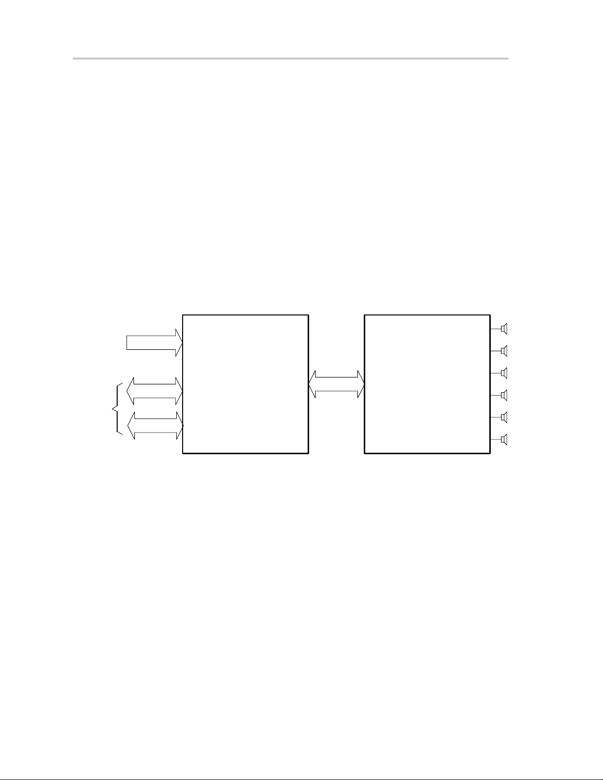
Figure 1–1.TDAA System With TAS5026REF and TAS5110D6REF Reference Designs
Digital
Audio
Interface
Control
Interface
I2S Bus
I2C Bus
Control Interface
1.1 TAS5026REF Features
- Six channel TDAA reference design (double-sided plated-through PCB
layout)
- Supports noiseless self-contained protection system (short circuit and
thermal) for the TAS5110 and the TAS5182 output stages. The
autorecovery loop is closed when JMP120 and JMP121 are shorted.
- Onboard headphone amplifier
TAS5026DREF
Module
PWM Interface
TAS5110D6REF
Module
1-2
Page 11

1.2 PCB Key Map
The physical structure for the TAS5026REF is illustrated in Figure 1–2.
Figure 1–2.Physical Structure for the TAS5026REF (Rough Outline)
PWM Interface
(J140)
Head–
Phone
Out
(J320)
Headphone Amplifier
Section
1.3 Jumper Settings
Together with the TAS5100/TAS5110/TAS5182 PWM output stages from
Texas Instruments, the TAS5026REF module can be configured in
autorecovery mode (closed loop). The SHUTDOWN
stage is connected to error recovery at the PWM processor when JMP120 and
JMP121 are shorted.
The autorecovery loop has to be disabled when the modulator board is
connected to an output stage module with autorecovery on-chip (e.g. the
TAS5111 and the TAS5112 reference modules). Autorecovery is disabled
when JMP120 and JMP 121 are removed.
PWM Processor
Section
Control Interface
(J100)
JMP120
JMP121
Digital Audio Interface
TI
TAS5026REF
(J160)
signal(s) from the output
1-3
Page 12

1-4
Page 13

Chapter 2
System Interfaces
This chapter describes the TAS5026REF system interfaces.
Topic Page
2.1 Digital Audio Interface (J160) 2-2. . . . . . . . . . . . . . . . . . . . . . . . . . . . . . . . . .
2.2 Control Interface (J100) 2-3. . . . . . . . . . . . . . . . . . . . . . . . . . . . . . . . . . . . . . . .
2.3 PWM Interface (J140) 2-5. . . . . . . . . . . . . . . . . . . . . . . . . . . . . . . . . . . . . . . . . .
2-1
Page 14

2.1 Digital Audio Interface (J160)
The digital audio interface contains digital audio signal data (I2S), clocks, etc.
See the T AS5026 data manual, SLES041, for signal timing and details not explained in this document.
Table 2–1.Digital Audio Interface Pin Connections
Pin No. Net Name Description
01 GND Ground
02 MCLK-IN Not used
03 GND
04 SDIN1 I2S data 1, channel 1 and 2 (left and right front speakers)
05 SDIN2 I2S data 2, channel 3 and 4 (left and right rear speakers)
06 SDIN3 I2S data 3, channel 5 and 6 (center speaker subwoofer)
07 GND Ground
08 GND Ground
09 GND Ground
10 GND Ground
11 SCLK I2S bit clock (64xFs) used to shift in serial data from SIN1, SDIN2, and SDIN3. SDA TA
12 GND Ground
13 LRCLK Left/right clock (Fs) used to indicate left/right data being transmitted in SDATA. The
14 GND Ground
15 Not used For future use
16 GND Ground
Ground
is sampled with the rising edge of the SCLK. The I2S format can be changed in the
2
I
C registers.
left channel is transmitted when LRCLK is low and the right channel is transmitted
when LRCLK is high.
Table 2–2.Clock Rates
Sample Frequency LRCLK (Fs) SCLK (64 × Fs) MCLK
Normal Speed
MCLK = 256 × Fs
Double Speed
MCLK = 256 × Fs
Quad Speed
Quad Speed
MCLK = 128 × Fs
2-2
32 kHz 32 kHz 2.048 MHz 8.192 MHz
44.1 kHz 44.1 kHz 2.8224 MHz 11.2896 MHz
48 kHz 48 kHz 3.072 MHz 12.288 MHz
64 kHz 64 kHz 4.096 MHz 16.384 MHz
88.2 kHz 88.2 kHz 5.6448 MHz 22.5792 MHz
96 kHz 96 kHz 6.144 MHz 24.576 MHz
176.4 kHz 176.4 kHz 1 1.2896 MHz 22.579 MHz
192 kHz 192 kHz 12.288 MHz 24.576 MHz
Page 15

2.2 Control Interface (J100)
The control interface connects the TAS5026 board to the microcontroller
section.
Table 2–3.Control Interface Pin Connections
Pin No. Net Name Description
01 GND Ground
02 V-HBRIDGE-CONTROL Not used
03 GND
04 RESET System reset (bidirectional). The TAS5026 enters a 4-ms initiation
05 SOFT–RESET TAS5026 error recovery (active low). Enables the user to enter a reset
06 MUTE MUTE (active low) ramps the volume from any setting to noiseless soft
07 POWER–DOWN POWER–DOWN (active low) places the T AS5026 in power-down mode.
08 Not used
09 Not used
10 SDA I2C data clock
11 GND Ground
12 SCL I2C bit clock
13 Not used
14 I2C–ADDRESS–SELECT TAS5026 I2C address
15 DOUBLE–SPEED DOUBLE–SPEED (active high) is used to support sampling rates of
16 CLIP Digital clipping indicator (active low)
17 GND Ground
18 DEM-SEL2
Ground
sequence before PWM signals are present at the output.
If a quit reset is desired, MUTE should be asserted low before applying
RESET
.
state click and pop free without resetting the I
settings.
Both soft and hard resets stop the output stage from switching and brings
it into a low-low state, meaning the low-side MOSFET in both half
bridges is ON.
mute.
Alternatively, the mute mode can also be initiated through the serial
control interface (I
During power down, all I
If a quit power down is desired, MUTE
applying RESET
select:
88.2 kHz and 96 kHz.
Alternatively, the double-speed mode can also be initiated through the
serial control interface (I
De-emphasis filter select bit 1
DEM-SEL2
0
0
1
1
2
C).
2
.
2
DEM-SEL1
0
1
0
1
C and data bus operations are ignored.
should be asserted low before
Pin Level
Low
High
C).
MODE
De-emphasis disabled
De-emphasis enabled for Fs = 32 kHz
De-emphasis enabled for Fs = 44.1 kHz
De-emphasis enabled for Fs = 48 kHz
2
C (volume) register
I2C Address
1Ah
1Bh
2-3
Page 16

Table 2–3. Control Interface Pin Connections (Continued)
Pin No. Net Name Description
19 DEM-SEL1 De-emphasis filter select bit 1
20 SD–E1 Shutdown error reporting group 1. The TAS51XX digital output stages
(channel 1, 2, and 5) assert this signal low when an internal error occurs.
This can be due to either an overtemperature protection or an overcurrent
event.
21 SD–E2 Shutdown error reporting group 2. The TAS51XX digital output stages
(channel 3, 4, and 6) assert this signal low when an internal error occurs.
This can be due to either an overtemperature protection or an overcurrent
event.
22 ERROR0 Error reporting 0 (ERR0 from the T AS51XX output stages)
23 ERROR1 Error reporting 1 (ERR1 from the T AS51XX output stages)
24 HEADPHONE–DISABLE
25
26 GND Ground
27 Not used For future use
28 Not used For future use
29 Not used For future use
30 Not used For future use
31 GND Ground
32 GND Ground
33 +5V Power supply (out)
34 +5V Power supply (out)
GND Ground
Headphone control
Headphone
enable sequence
Headphone
disable sequence
Headphone
disable mode
1. Mute all channels (register address 03h)
2. HEADPHONE–DISABLE
3. Individual channel mute of channels 3–6
(register address 19h).
4. Unmute all channels (register address 03h).
1. Mute all channels (register address 03h)
2. HEADPHONE–DISABLE
3. Unmute of channels 3–6 (register address
19h).
4. Unmute all channels (register address 03h).
0 Headphone output disabled.
1 Output stage channel 1 and 2 is muted.
Channel 3, 4, 5, and 6 should be muted
through the I
2
C interface.
is asserted high.
is asserted low.
2-4
Page 17

2.3 PWM Interface (J140)
The PWM interface connects the TAS5026REF board to the output stage
module.
Figure 2–1.Pin Numbers at PWM Interface (J140)
2
64 89710 12
31 5
1311 15
1614 18
20 22
1917
2321 25
2624 28
30 32
2927
3331 35
3634 38
40 42
3937
Table 2–4.J140 Pin Description
Pin No. Net Name Description
01 V-HBRIDGE-CONTROL For future use
02 GND Ground
03 PWM–AP–1
04 PWM–AM–1 Channel 1 PWM input (differential –) – positive H-bridge side
05 VALID–1 Valid channel 1
06 PWM–BM–1 Channel 1 PWM input (differential –) – negative H-bridge side
07 PWM–BP–1 Channel 1 PWM input (differential +) – negative H-bridge side
08 GND Ground
09 PWM–AP–2 Channel 2 PWM input (differential +) – positive H-bridge side
10 PWM–AM–2 Channel 2 PWM input (differential –) – positive H-bridge side
11 VALID–2 Valid channel 2
12 PWM–BM–2 Channel 2 PWM input (differential –) – negative H-bridge side
13 PWM–BP–2 Channel 2 PWM input (differential +) – negative H-bridge side
14 GND Ground
15 PWM–AP–3 Channel 3 PWM input (differential +) – positive H-bridge side
16 PWM–AM–3 Channel 3 PWM input (differential –) – positive H-bridge side
17 VALID–3 Valid channel 3
18 PWM–BM–3 Channel 3 PWM input (differential –) – negative H-bridge side
19 PWM–BP–3 Channel 3 PWM input (differential +) – negative H-bridge side
20 GND Ground
21 PWM–AP–4 Channel 4 PWM input (differential +) – positive H-bridge side
22 PWM–AM–4 Channel 4 PWM input (differential –) – positive H-bridge side
23 VALID–4 Valid channel 4
24 PWM–BM–4 Channel 4 PWM input (differential –) – negative H-bridge side
25 PWM–BP–4 Channel 4 PWM input (differential +) – negative H-bridge side
26 GND Ground
27 PWM–AP–5 Channel 5 PWM input (differential +) – positive H-bridge side
Channel 1 PWM input (differential +) – positive H-bridge side
4341 45
4644 48
50
4947
2-5
Page 18

Table 2–4. J100 Pin Description (Continued)
Pin No. Net Name Description
28 PWM–AM–5 Channel 5 PWM input (differential –) – positive H-bridge side
29 VALID–5 Valid channel 5
30 PWM–BM–5 Channel 5 PWM input (differential –) – negative H-bridge side
31 PWM–BP–5 Channel 5 PWM input (differential +) – negative H-bridge side
32 GND Ground
33 PWM–AP–6 Channel 6 PWM input (differential +) – positive H-bridge side
34 PWM–AM–6 Channel 6 PWM input (differential –) – positive H-bridge side
35 VALID–6 Valid channel 6
36 PWM–BM–6 Channel 6 PWM input (differential –) – negative H-bridge side
37 PWM–BP–6 Channel 6 PWM input (differential +) – negative H-bridge side
38 SD–E1 Shutdown group 1 (center + left and right front speakers)
39 SD–E2 Shutdown group 2 (subwoofer + left and right rear speakers)
40 ERROR0 Error signal ERR0 from TAS5110
41 ERROR1 Error signal ERR1 from TAS5110
42 RESET System reset (bidirectional)
43 PSU–COMP–2 For future use
44 PSU–COMP–1 For future use
45 Not Used For future use
46 Not Used For future use
47 +3.3V 3.3-V supply voltage for the modulator module (e.g., the T AS5026REF)
48 GND Ground
49 +5V 5-V supply voltage
50 +5V 5-V supply voltage
2-6
Page 19

Chapter 3
Schematic, Parts List, PCB Specification, and
PCB Layout
The chapter contains the schematic, parts list, PCB specification, and PCB
layout for the TAS5026REF.
3-1
Page 20

Input & Output Section
TI
TI
TAS5026REF
DIGITAL AUDIO GROUP
DIGITAL AUDIO GROUP
ALL RIGHTS RESERVED - PATENTS PENDING
ALL RIGHTS RESERVED - PATENTS PENDING
TEXAS INSTRUMENTS INCORPORATED
TEXAS INSTRUMENTS INCORPORATED
Page 21

TAS5026 Section
TI
TI
TAS5026REF
DIGITAL AUDIO GROUP
DIGITAL AUDIO GROUP
ALL RIGHTS RESERVED - PATENTS PENDING
ALL RIGHTS RESERVED - PATENTS PENDING
TEXAS INSTRUMENTS INCORPORATED
TEXAS INSTRUMENTS INCORPORATED
Page 22

Headphone Amplifier Section
TI
TI
TAS5026REF
DIGITAL AUDIO GROUP
DIGITAL AUDIO GROUP
ALL RIGHTS RESERVED - PATENTS PENDING
ALL RIGHTS RESERVED - PATENTS PENDING
TEXAS INSTRUMENTS INCORPORATED
TEXAS INSTRUMENTS INCORPORATED
Page 23

TI
TAS5026REF Parts List
Ref Des Part Number Description Housing Manufacturer Manufacturer Part Number
C100 200041060 10 uF 16 V 20% LYT LY4x5SMD Panasonic ECE V 1C A 100 SR
C140 200041060 10 uF 16 V 20% LYT LY4x5SMD Panasonic ECE V 1C A 100 SR
C200 Not used Not used
C201 200054730 47 nF 16 V 20% X7R 0603 KEMET C0603C473M2RAC
C202 200054720 4.7 nF 50 V 20% X7R 0603 KEMET C0603C473M5RAC
C203 200041060 10 uF 16 V 20% LYT LY4x5SMD Panasonic ECE V 1C A 100 SR
C204 200051040 100 nF 16 V 20% X7R 0603 KEMET C0603C104M4RAC
C205 Not used Not used
C206 200052240 220 nF 10 V 10% X7R 0603 Phycomp 223824615654
C207 200052240 220 nF 10 V 10% X7R 0603 Phycomp 223824615654
C208 Not used Not used
C300 200051040 100 nF 16 V 20% X7R 0603 KEMET C0603C104M4RAC
C320 200064710 470 pF 10% 50 V NP0 0603 KEMET C0603C471K5GAC
C321 200064710 470 pF 10% 50 V NP0 0603 KEMET C0603C471K5GAC
C322 200064710 470 pF 10% 50 V NP0 0603 KEMET C0603C471K5GAC
C323 200064710 470 pF 10% 50 V NP0 0603 KEMET C0603C471K5GAC
C324 200062210 220 pF 10% 50 V NP0 0603 KEMET C0603C221K5GAC
C325 200051040 100 nF 16 V 20% X7R 0603 KEMET C0603C104M4RAC
C326 200041060 10 uF 16 V 20% LYT LY4x5SMD Panasonic ECE V 1C A 100 SR
C327 200062210 220 pF 10% 50 V NP0 0603 KEMET C0603C221K5GAC
C328 200062210 220 pF 10% 50 V NP0 0603 KEMET C0603C221K5GAC
C329 200062210 220 pF 10% 50 V NP0 0603 KEMET C0603C221K5GAC
C330 200051040 100 nF 16 V 20% X7R 0603 KEMET C0603C104M4RAC
C331 200042270 220 uF 6.3 V 20% LYT LY8x9SMD Panasonic EEV F C0 J 221 P
C332 Deleted Deleted
C333 Deleted Deleted
J100 700820340 Box Header straight 34 pin 2.54 mm IDC34 Multicomp MC9A12-3434
J140 700820500 Box Header straight 50 pin 2.54 mm IDC50 Multicomp MC9A12-5034
J160 700820160 Box Header straight 16 pin 2,54 mm IDC16 Multicomp MC9A12-1634
J320 700353520 Stereo 3,5 mm jack socket Schurter 4832.2320
JMP120 700100020 2 pin 2,54 mm pitch header MX2SI Molex 90120-0122
JMP121 700100020 2 pin 2,54 mm pitch Header MX2SI Molex 90120-0122
PCB 900116412 P164-PCB-001(3.00) Printline P164-PCB-001(3.00)
R100 100210020 10 khm0 5% 200 ppm 100 mW metalfilm 0603 BC Components DCT 0603 - 00 5% PA 10k0
R101 100210020 10 kohm 5% 200 ppm 100 mW metalfilm 0603 BC Components DCT 0603 - 00 5% PA 10k0
R102 100210020 10 kohm 5% 200 ppm 100 mW metalfilm 0603 BC Components DCT 0603 - 00 5% PA 10k0
R103 100210020 10 kohm 5% 200 ppm 100 mW metalfilm 0603 BC Components DCT 0603 - 00 5% PA 10k0
R104 Not used Not used
Texas Instruments, Digital Audio & Video
Page 24

TI
TAS5026REF Parts List
Ref Des Part Number Description Housing Manufacturer Manufacturer Part Number
R105 100210020 10 kohm 5% 200 ppm 100 mW metalfilm 0603 BC Components DCT 0603 - 00 5% PA 10k0
R106 100210020 10 kohm 5% 200 ppm 100 mW metalfilm 0603 BC Components DCT 0603 - 00 5% PA 10k0
R107 100210020 10 kohm 5% 200 ppm 100 mW metalfilm 0603 BC Components DCT 0603 - 00 5% PA 10k0
R108 100210020 10 kohm 5% 200 ppm 100 mW metalfilm 0603 BC Components DCT 0603 - 00 5% PA 10k0
R109 100210020 10 kohm 5% 200 ppm 100 mW metalfilm 0603 BC Components DCT 0603 - 00 5% PA 10k0
R120 100210020 10 kohm 5% 200 ppm 100 mW metalfilm 0603 BC Components DCT 0603 - 00 5% PA 10k0
R121 100210020 10 kohm 5% 200 ppm 100 mW metalfilm 0603 BC Components DCT 0603 - 00 5% PA 10k0
R160 100247090 47 R0 5% 200 ppm 100 mW metalfilm 0603 BC Components DCT 0603 -00 5% PA 47R0
R161 100247090 47 R0 5% 200 ppm 100 mW metalfilm 0603 BC Components DCT 0603 -00 5% PA 47R0
R162 100247090 47 R0 5% 200 ppm 100 mW metalfilm 0603 BC Components DCT 0603 -00 5% PA 47R0
R163 100247090 47 R0 5% 200 ppm 100 mW metalfilm 0603 BC Components DCT 0603 -00 5% PA 47R0
R164 100247090 47 R0 5% 200 ppm 100 mW metalfilm 0603 BC Components DCT 0603 -00 5% PA 47R0
R200 100210020 10 khm 5% 200 ppm 100 mW metalfilm 0603 BC Components DCT 0603 - 00 5% PA 10k0
R201 100210020 10 kohm 5% 200 ppm 100 mW metalfilm 0603 BC Components DCT 0603 - 00 5% PA 10k0
R202 100222000 220 R 5% 200 ppm 100 mW metalfilm 0603 BC Components DCT 0603 -00 5% PA 220R
R203 100247090 47 R0 5% 200 ppm 100 mW metalfilm 0603 BC Components DCT 0603 -00 5% PA 47R0
R204 100210080 1 R0 5% 300 ppm 100 mW metalfilm 0603 BC Components DCT 0603 -00 5% PA 1R0
R205 100247080 4 R70 5% 300 ppm 100 mW metalfilm 0603 BC Components DCT 0603 -00 5% PA 4R70
R206 Deleted Deleted
R207 Deleted Deleted
R208 100222090 22 R 5% 200 ppm 100 mW metalfilm 0603 BC Components DCT 0603 -00 5% PA 22R
R209 100247080 4 R70 5% 300 ppm 100 mW metalfilm 0603 BC Components DCT 0603 -00 5% PA 4R70
R320 100282010 8 k20 5% 200 ppm 100 mW metalfilm 0603 BC Components DCT 0603 -00 5% PA 8k20
R321 100282010 8 k20 5% 200 ppm 100 mW metalfilm 0603 BC Components DCT 0603 -00 5% PA 8k20
R322 100282010 8 k20 5% 200 ppm 100 mW metalfilm 0603 BC Components DCT 0603 -00 5% PA 8k20
R323 100282010 8 k20 5% 200 ppm 100 mW metalfilm 0603 BC Components DCT 0603 -00 5% PA 8k20
R324 100210020 10 k0 5% 200 ppm 100 mW metalfilm 0603 BC Components DCT 0603 - 00 5% PA 10k0
R325 100210020 10 k0 5% 200 ppm 100 mW metalfilm 0603 BC Components DCT 0603 - 00 5% PA 10k0
R326 100210020 10 k0 5% 200 ppm 100 mW metalfilm 0603 BC Components DCT 0603 - 00 5% PA 10k0
R327 100210020 10 k0 5% 200 ppm 100 mW metalfilm 0603 BC Components DCT 0603 - 00 5% PA 10k0
R328 100282010 8 k20 5% 200 ppm 100 mW metalfilm 0603 BC Components DCT 0603 -00 5% PA 8k20
R329 100282010 8 k20 5% 200 ppm 100 mW metalfilm 0603 BC Components DCT 0603 -00 5% PA 8k20
R330 100282010 8 k20 5% 200 ppm 100 mW metalfilm 0603 BC Components DCT 0603 -00 5% PA 8k20
R331 100282010 8 k20 5% 200 ppm 100 mW metalfilm 0603 BC Components DCT 0603 -00 5% PA 8k20
R332 100210010 1 k00 5% 200 ppm 100 mW metalfilm 0603 BC Components DCT 0603 - 00 5% PA 1k00
R333 100210010 1 k00 5% 200 ppm 100 mW metalfilm 0603 BC Components DCT 0603 - 00 5% PA 1k00
R334 100210010 1 k00 5% 200 ppm 100 mW metalfilm 0603 BC Components DCT 0603 - 00 5% PA 1k00
R335 100210010 1 k00 5% 200 ppm 100 mW metalfilm 0603 BC Components DCT 0603 - 00 5% PA 1k00
Texas Instruments, Digital Audio & Video
Page 25

Texas Instruments
TQFP64
Texas Instruments
TAS5026APFB
Texas Instruments
TSSOP14
Texas Instruments
TSSOP14
Texas Instruments
Texas Instruments
TPA112DGN
TI
TAS5026REF Parts List
Ref Des Part Number Description Housing Manufacturer Manufacturer Part Number
SHUNT120 700110210 Black 2,54 mm shunt Molex 15-29-1024
SHUNT121 700110210 Black 2,54 mm shunt Molex 15-29-1024
U120 520140083 Dual AND gate, LVC MSOP8
U200 500050261 6 ch PWM processor (AD, VOL, 192kHz)
U300 520140140 Single Schmitt-Trigger Inverter, LVC SOT23-5
U301 520140081 Quad AND gate, LVC
U302 520141262 Quad buffer with output enable, LVC
U320 510101121 150-mW stereo power amplifier MSOP8
SN74LVC2G08DCTR
SN74LVC1G14DBVR
SN74LVC08APWR
SN74LVC126APWR
Texas Instruments, Digital Audio & Video
Page 26

TI TAS5026REF PCB SPECIFICATION
TAS5026REF PCB SPECIFICATION
BOARD IDENTIFICATION: P164-PCB-001 (3.00)
BOARD TYPE: DOUBLE-SIDED PLATED-THROUGH BOARD
LAMINATE TYPE: FR4
LAMINATE THICKNESS: 1.6 mm
COPPER THICKNESS: 35µm (INCL. PLATING EXTERIOR LAYER)
COPPER PLATING OF HOLES: >25µm
MINIMUM HOLE DIAMETER 0.3 mm
SILKSCREEN COMPONENT SIDE: WHITE - REMOVE SILKSCREEN FROM SOLDER AREA & PRE-TINNED AREAS
SILKSCREEN SOLDER SIDE: None
SOLDER MASK COMPONENT SIDE: GREEN
SOLDER MASK SOLDER SIDE: GREEN
PROTECTIVE COATING: SOLDER COATING AND CHEMICAL SILVER ON FREE COPPER
ELECTRICAL TEST: PCB MUST BE ELECTRICAL TESTED
MANUFACTURED TO: PERFAG 2E (www.perfag.dk)
APERTURE TABLE: PERFAG 10A (www.perfag.dk)
BOARD SIZE: 127 x 44 mm
Page 27

Page 28

Page 29

Page 30

Page 31

 Loading...