

Page 1

查询TAS5026供应商
Data Manual
November 2002 DAV Digital Audio/Speaker
SLES041B
Page 2

IMPORTANT NOTICE
Texas Instruments Incorporated and its subsidiaries (TI) reserve the right to make corrections, modifications,
enhancements, improvements, and other changes to its products and services at any time and to discontinue
any product or service without notice. Customers should obtain the latest relevant information before placing
orders and should verify that such information is current and complete. All products are sold subject to TI’s terms
and conditions of sale supplied at the time of order acknowledgment.
TI warrants performance of its hardware products to the specifications applicable at the time of sale in
accordance with TI’s standard warranty . Testing and other quality control techniques are used to the extent TI
deems necessary to support this warranty . Except where mandated by government requirements, testing of all
parameters of each product is not necessarily performed.
TI assumes no liability for applications assistance or customer product design. Customers are responsible for
their products and applications using TI components. T o minimize the risks associated with customer products
and applications, customers should provide adequate design and operating safeguards.
TI does not warrant or represent that any license, either express or implied, is granted under any TI patent right,
copyright, mask work right, or other TI intellectual property right relating to any combination, machine, or process
in which TI products or services are used. Information published by TI regarding third–party products or services
does not constitute a license from TI to use such products or services or a warranty or endorsement thereof.
Use of such information may require a license from a third party under the patents or other intellectual property
of the third party , or a license from TI under the patents or other intellectual property of TI.
Reproduction of information in TI data books or data sheets is permissible only if reproduction is without
alteration and is accompanied by all associated warranties, conditions, limitations, and notices. Reproduction
of this information with alteration is an unfair and deceptive business practice. TI is not responsible or liable for
such altered documentation.
Resale of TI products or services with statements different from or beyond the parameters stated by TI for that
product or service voids all express and any implied warranties for the associated TI product or service and
is an unfair and deceptive business practice. TI is not responsible or liable for any such statements.
Mailing Address:
Texas Instruments
Post Office Box 655303
Dallas, Texas 75265
Copyright 2002, Texas Instruments Incorporated
Page 3

Contents
Contents
Section Page
1 Introduction 1. . . . . . . . . . . . . . . . . . . . . . . . . . . . . . . . . . . . . . . . . . . . . . . . . . . . . . . . . . . . . . . . . . . . . . . . . . . .
1.1 Features 1. . . . . . . . . . . . . . . . . . . . . . . . . . . . . . . . . . . . . . . . . . . . . . . . . . . . . . . . . . . . . . . . . . . . . . . .
1.2 Functional Block Diagram 2. . . . . . . . . . . . . . . . . . . . . . . . . . . . . . . . . . . . . . . . . . . . . . . . . . . . . . . . . .
1.3 Terminal Assignments 3. . . . . . . . . . . . . . . . . . . . . . . . . . . . . . . . . . . . . . . . . . . . . . . . . . . . . . . . . . . . .
1.4 Ordering Information 4. . . . . . . . . . . . . . . . . . . . . . . . . . . . . . . . . . . . . . . . . . . . . . . . . . . . . . . . . . . . . .
1.5 Terminal Functions 4. . . . . . . . . . . . . . . . . . . . . . . . . . . . . . . . . . . . . . . . . . . . . . . . . . . . . . . . . . . . . . . .
2 Architecture Overview 6. . . . . . . . . . . . . . . . . . . . . . . . . . . . . . . . . . . . . . . . . . . . . . . . . . . . . . . . . . . . . . . . . .
2.1 Clock and Serial Data Interface 6. . . . . . . . . . . . . . . . . . . . . . . . . . . . . . . . . . . . . . . . . . . . . . . . . . . . .
2.1.1 Normal-Speed, Double-Speed, and Quad-Speed Selection 6. . . . . . . . . . . . . . . . . . .
2.1.2 Clock Master/Slave Mode (M_S) 7. . . . . . . . . . . . . . . . . . . . . . . . . . . . . . . . . . . . . . . . . .
2.1.3 Clock Master Mode 7. . . . . . . . . . . . . . . . . . . . . . . . . . . . . . . . . . . . . . . . . . . . . . . . . . . . . .
2.1.4 Clock Slave Mode 8. . . . . . . . . . . . . . . . . . . . . . . . . . . . . . . . . . . . . . . . . . . . . . . . . . . . . . .
2.1.5 PLL Filter 10. . . . . . . . . . . . . . . . . . . . . . . . . . . . . . . . . . . . . . . . . . . . . . . . . . . . . . . . . . . . . .
2.1.6 DCLK 10. . . . . . . . . . . . . . . . . . . . . . . . . . . . . . . . . . . . . . . . . . . . . . . . . . . . . . . . . . . . . . . . . .
2.1.7 Serial Data Interface 10. . . . . . . . . . . . . . . . . . . . . . . . . . . . . . . . . . . . . . . . . . . . . . . . . . . . .
2.2 Reset, Power Down, and Status 15. . . . . . . . . . . . . . . . . . . . . . . . . . . . . . . . . . . . . . . . . . . . . . . . . . . .
2.2.1 Reset—RESET 15. . . . . . . . . . . . . . . . . . . . . . . . . . . . . . . . . . . . . . . . . . . . . . . . . . . . . . . . .
2.2.2 Power Down—PDN 16. . . . . . . . . . . . . . . . . . . . . . . . . . . . . . . . . . . . . . . . . . . . . . . . . . . . .
2.2.3 Status Registers 16. . . . . . . . . . . . . . . . . . . . . . . . . . . . . . . . . . . . . . . . . . . . . . . . . . . . . . . .
2.3 Signal Processing 17. . . . . . . . . . . . . . . . . . . . . . . . . . . . . . . . . . . . . . . . . . . . . . . . . . . . . . . . . . . . . . . .
2.3.1 Volume Control 17. . . . . . . . . . . . . . . . . . . . . . . . . . . . . . . . . . . . . . . . . . . . . . . . . . . . . . . . .
2.3.2 Mute 18. . . . . . . . . . . . . . . . . . . . . . . . . . . . . . . . . . . . . . . . . . . . . . . . . . . . . . . . . . . . . . . . . .
2.3.3 Auto Mute 18. . . . . . . . . . . . . . . . . . . . . . . . . . . . . . . . . . . . . . . . . . . . . . . . . . . . . . . . . . . . . .
2.3.4 Individual Channel Mute 18. . . . . . . . . . . . . . . . . . . . . . . . . . . . . . . . . . . . . . . . . . . . . . . . . .
2.3.5 De-Emphasis Filter 18. . . . . . . . . . . . . . . . . . . . . . . . . . . . . . . . . . . . . . . . . . . . . . . . . . . . . .
2.4 Pulse Width Modulator (PWM) 19. . . . . . . . . . . . . . . . . . . . . . . . . . . . . . . . . . . . . . . . . . . . . . . . . . . . . .
2.4.1 Clipping Indicator 19. . . . . . . . . . . . . . . . . . . . . . . . . . . . . . . . . . . . . . . . . . . . . . . . . . . . . . . .
2.4.2 Error Recovery 19. . . . . . . . . . . . . . . . . . . . . . . . . . . . . . . . . . . . . . . . . . . . . . . . . . . . . . . . .
2.4.3 Individual Channel Error Recovery 20. . . . . . . . . . . . . . . . . . . . . . . . . . . . . . . . . . . . . . . . .
2.4.4 PWM DC-Offset Correction 20. . . . . . . . . . . . . . . . . . . . . . . . . . . . . . . . . . . . . . . . . . . . . . .
2.4.5 Inter-Channel Delay 20. . . . . . . . . . . . . . . . . . . . . . . . . . . . . . . . . . . . . . . . . . . . . . . . . . . . .
2.4.6 PWM/H-Bridge and Discrete H-Bridge Driver Interface 20. . . . . . . . . . . . . . . . . . . . . . .
2.5 I2C Serial Control Interface 21. . . . . . . . . . . . . . . . . . . . . . . . . . . . . . . . . . . . . . . . . . . . . . .
2.5.1 Single Byte Write 22. . . . . . . . . . . . . . . . . . . . . . . . . . . . . . . . . . . . . . . . . . . . . . . . . . . . . . . .
2.5.2 Multiple Byte Write 22. . . . . . . . . . . . . . . . . . . . . . . . . . . . . . . . . . . . . . . . . . . . . . . . . . . . . .
2.5.3 Single Byte Read 22. . . . . . . . . . . . . . . . . . . . . . . . . . . . . . . . . . . . . . . . . . . . . . . . . . . . . . . .
2.5.4 Multiple Byte Read 23. . . . . . . . . . . . . . . . . . . . . . . . . . . . . . . . . . . . . . . . . . . . . . . . . . . . . .
3 Serial Control Interface Register Definitions 24. . . . . . . . . . . . . . . . . . . . . . . . . . . . . . . . . . . . . . . . . . . . . .
3.1 General Status Register (x00) 25. . . . . . . . . . . . . . . . . . . . . . . . . . . . . . . . . . . . . . . . . . . . . . . . . . . . . .
3.2 Error Status Register (x01) 25. . . . . . . . . . . . . . . . . . . . . . . . . . . . . . . . . . . . . . . . . . . . . . . . . . . . . . . . .
3.3 System Control Register 0 (x02) 25. . . . . . . . . . . . . . . . . . . . . . . . . . . . . . . . . . . . . . . . . . . . . . . . . . . .
3.4 System Control Register 1 (x03) 26. . . . . . . . . . . . . . . . . . . . . . . . . . . . . . . . . . . . . . . . . . . . . . . . . . . .
3.5 Error Recovery Register (x04) 26. . . . . . . . . . . . . . . . . . . . . . . . . . . . . . . . . . . . . . . . . . . . . . . . . . . . . .
3.6 Automute Delay Register (x05) 26. . . . . . . . . . . . . . . . . . . . . . . . . . . . . . . . . . . . . . . . . . . . . . . . . . . . .
3.7 DC-Offset Control Registers (x06–x0B) 27. . . . . . . . . . . . . . . . . . . . . . . . . . . . . . . . . . . . . . . . . . . . . .
3.8 Interchannel Delay Registers (x0C–x11) 27. . . . . . . . . . . . . . . . . . . . . . . . . . . . . . . . . . . . . . . . . . . . .
November 2002 SLES041B
iii
Page 4

List of Illustrations
3.9 Individual Channel Mute Register (x19) 27. . . . . . . . . . . . . . . . . . . . . . . . . . . . . . . . . . . . . . . . . . . . . .
4 System Initialization 28. . . . . . . . . . . . . . . . . . . . . . . . . . . . . . . . . . . . . . . . . . . . . . . . . . . . . . . . . . . . . . . . . . . .
5 Specifications 29. . . . . . . . . . . . . . . . . . . . . . . . . . . . . . . . . . . . . . . . . . . . . . . . . . . . . . . . . . . . . . . . . . . . . . . . . .
5.1 Absolute Maximum Ratings Over Operating Temperature Ranges 29. . . . . . . . . . . . . . . . . . . . . . .
5.2 Recommended Operating Conditions 29. . . . . . . . . . . . . . . . . . . . . . . . . . . . . . . . . . . . . . . . . . . . . . . .
5.3 Electrical Characteristics 29. . . . . . . . . . . . . . . . . . . . . . . . . . . . . . . . . . . . . . . . . . . . . . . . . . . . . . . . . . .
5.3.1 Static Digital Specifications 29. . . . . . . . . . . . . . . . . . . . . . . . . . . . . . . . . . . . . . . . . . . . . . .
5.3.2 Digital Interpolation Filter and PWM Modulator 29. . . . . . . . . . . . . . . . . . . . . . . . . . . . . .
5.3.3 TAS5026/TAS5100 System Performance Measured at the Speaker Terminals 30. . .
5.4 Switching Characteristics 30. . . . . . . . . . . . . . . . . . . . . . . . . . . . . . . . . . . . . . . . . . . . . . . . . . . . . . . . . .
5.4.1 Command Sequence Timing 30. . . . . . . . . . . . . . . . . . . . . . . . . . . . . . . . . . . . . . . . . . . . . .
5.4.2 Serial Audio Port 34. . . . . . . . . . . . . . . . . . . . . . . . . . . . . . . . . . . . . . . . . . . . . . . . . . . . . . . .
5.4.3 Serial Control Port—I2C Operation 37. . . . . . . . . . . . . . . . . . . . . . . . . . . . . . . . . . . . . . . .
6 Application Information 38. . . . . . . . . . . . . . . . . . . . . . . . . . . . . . . . . . . . . . . . . . . . . . . . . . . . . . . . . . . . . . . . .
6.1 Serial Audio Interface Clock Master and Slave Interface Configuration 39. . . . . . . . . . . . . . . . . . .
6.1.1 Slave Configuration 39. . . . . . . . . . . . . . . . . . . . . . . . . . . . . . . . . . . . . . . . . . . . . . . . . . . . . .
6.1.2 Master Configuration 39. . . . . . . . . . . . . . . . . . . . . . . . . . . . . . . . . . . . . . . . . . . . . . . . . . . .
7 Mechanical Data 40. . . . . . . . . . . . . . . . . . . . . . . . . . . . . . . . . . . . . . . . . . . . . . . . . . . . . . . . . . . . . . . . . . . . . . . .
List of Illustrations
Figure Title Page
2–1 Crystal Circuit 8. . . . . . . . . . . . . . . . . . . . . . . . . . . . . . . . . . . . . . . . . . . . . . . . . . . . . . . . . . . . . . . . . . . . . . . . . .
2–2 External PLL Loop Filter 10. . . . . . . . . . . . . . . . . . . . . . . . . . . . . . . . . . . . . . . . . . . . . . . . . . . . . . . . . . . . . . . . .
2–3 I2S 64-Fs Format 11. . . . . . . . . . . . . . . . . . . . . . . . . . . . . . . . . . . . . . . . . . . . . . . . . . . . . . . . . . . . . . . . . . . . . . .
2–4 I2S 48-Fs Format 12. . . . . . . . . . . . . . . . . . . . . . . . . . . . . . . . . . . . . . . . . . . . . . . . . . . . . . . . . . . . . . . . . . . . . . .
2–5 Left-Justified 64-Fs Format 12. . . . . . . . . . . . . . . . . . . . . . . . . . . . . . . . . . . . . . . . . . . . . . . . . . . . . . . . . . . . . . .
2–6 Left-Justified 48-Fs Format 13. . . . . . . . . . . . . . . . . . . . . . . . . . . . . . . . . . . . . . . . . . . . . . . . . . . . . . . . . . . . . . .
2–7 Right-Justified 64-Fs Format 13. . . . . . . . . . . . . . . . . . . . . . . . . . . . . . . . . . . . . . . . . . . . . . . . . . . . . . . . . . . . . .
2–8 Right-Justified 48-Fs Format 14. . . . . . . . . . . . . . . . . . . . . . . . . . . . . . . . . . . . . . . . . . . . . . . . . . . . . . . . . . . . . .
2–9 DSP Format 14. . . . . . . . . . . . . . . . . . . . . . . . . . . . . . . . . . . . . . . . . . . . . . . . . . . . . . . . . . . . . . . . . . . . . . . . . . . .
2–10 Attenuation Curve 17. . . . . . . . . . . . . . . . . . . . . . . . . . . . . . . . . . . . . . . . . . . . . . . . . . . . . . . . . . . . . . . . . . . . . .
2–11 De-Emphasis Filter Characteristics 19. . . . . . . . . . . . . . . . . . . . . . . . . . . . . . . . . . . . . . . . . . . . . . . . . . . . . . .
2–12 PWM Outputs and H-Bridge Driven in BTL Configuration 21. . . . . . . . . . . . . . . . . . . . . . . . . . . . . . . . . . . .
2–13 Typical I2C Sequence 21. . . . . . . . . . . . . . . . . . . . . . . . . . . . . . . . . . . . . . . . . . . . . . . . . . . . . . . . . . . . . . . . . .
2–14 Single Byte Write Transfer 22. . . . . . . . . . . . . . . . . . . . . . . . . . . . . . . . . . . . . . . . . . . . . . . . . . . . . . . . . . . . . .
2–15 Multiple Byte Write Transfer 22. . . . . . . . . . . . . . . . . . . . . . . . . . . . . . . . . . . . . . . . . . . . . . . . . . . . . . . . . . . . .
2–16 Single Byte Read 22. . . . . . . . . . . . . . . . . . . . . . . . . . . . . . . . . . . . . . . . . . . . . . . . . . . . . . . . . . . . . . . . . . . . . .
2–17 Multiple Byte Read 23. . . . . . . . . . . . . . . . . . . . . . . . . . . . . . . . . . . . . . . . . . . . . . . . . . . . . . . . . . . . . . . . . . . . .
4–1 RESET During System Initialization 28. . . . . . . . . . . . . . . . . . . . . . . . . . . . . . . . . . . . . . . . . . . . . . . . . . . . . . . .
5–1 RESET Timing 30. . . . . . . . . . . . . . . . . . . . . . . . . . . . . . . . . . . . . . . . . . . . . . . . . . . . . . . . . . . . . . . . . . . . . . . . . .
5–2 Power-Down and Power-Up Timing—RESET Preceding PDN 31. . . . . . . . . . . . . . . . . . . . . . . . . . . . . . . . .
5–3 Power-Down and Power-Up Timing—RESET Following PDN 32. . . . . . . . . . . . . . . . . . . . . . . . . . . . . . . . .
5–4 Error Recovery Timing 33. . . . . . . . . . . . . . . . . . . . . . . . . . . . . . . . . . . . . . . . . . . . . . . . . . . . . . . . . . . . . . . . . . .
5–5 Mute Timing 33. . . . . . . . . . . . . . . . . . . . . . . . . . . . . . . . . . . . . . . . . . . . . . . . . . . . . . . . . . . . . . . . . . . . . . . . . . . .
iv
November 2002SLES041B
Page 5

List of Tables
5–6 Right-Justified, IIS, Left-Justified Serial Protocol Timing 34. . . . . . . . . . . . . . . . . . . . . . . . . . . . . . . . . . . . . .
5–7 Right, Left, and IIS Serial Mode Timing Requirement 35. . . . . . . . . . . . . . . . . . . . . . . . . . . . . . . . . . . . . . . . .
5–8 Serial Audio Ports Master Mode Timing 35. . . . . . . . . . . . . . . . . . . . . . . . . . . . . . . . . . . . . . . . . . . . . . . . . . . .
5–9 DSP Serial Port Timing 35. . . . . . . . . . . . . . . . . . . . . . . . . . . . . . . . . . . . . . . . . . . . . . . . . . . . . . . . . . . . . . . . . .
5–10 DSP Serial Port Expanded Timing 36. . . . . . . . . . . . . . . . . . . . . . . . . . . . . . . . . . . . . . . . . . . . . . . . . . . . . . . .
5–11 DSP Absolute Timing 36. . . . . . . . . . . . . . . . . . . . . . . . . . . . . . . . . . . . . . . . . . . . . . . . . . . . . . . . . . . . . . . . . . .
5–12 SCL and SDA Timing 37. . . . . . . . . . . . . . . . . . . . . . . . . . . . . . . . . . . . . . . . . . . . . . . . . . . . . . . . . . . . . . . . . . .
5–13 Start and Stop Conditions Timing 37. . . . . . . . . . . . . . . . . . . . . . . . . . . . . . . . . . . . . . . . . . . . . . . . . . . . . . . . .
6–1 Typical TAS5026 Application 38. . . . . . . . . . . . . . . . . . . . . . . . . . . . . . . . . . . . . . . . . . . . . . . . . . . . . . . . . . . . . .
6–2 TAS5026 Serial Audio Port—Slave Mode Connection Diagram 39. . . . . . . . . . . . . . . . . . . . . . . . . . . . . . . .
6–3 TAS5026 Serial Audio Port—Master Mode Connection Diagram 39. . . . . . . . . . . . . . . . . . . . . . . . . . . . . . .
List of Tables
Table Title Page
2–1 Normal-Speed, Double-Speed, and Quad-Speed Operation 7. . . . . . . . . . . . . . . . . . . . . . . . . . . . . . . . . . .
2–2 Master and Slave Clock Modes 9. . . . . . . . . . . . . . . . . . . . . . . . . . . . . . . . . . . . . . . . . . . . . . . . . . . . . . . . . . .
2–3 LRCLK, MCLK_IN, and External PLL Rates 9. . . . . . . . . . . . . . . . . . . . . . . . . . . . . . . . . . . . . . . . . . . . . . . .
2–4 DCLK 10. . . . . . . . . . . . . . . . . . . . . . . . . . . . . . . . . . . . . . . . . . . . . . . . . . . . . . . . . . . . . . . . . . . . . . . . . . . . . . . . .
2–5 Supported Word Lengths 11. . . . . . . . . . . . . . . . . . . . . . . . . . . . . . . . . . . . . . . . . . . . . . . . . . . . . . . . . . . . . . . . .
2–6 Device Outputs During Reset 15. . . . . . . . . . . . . . . . . . . . . . . . . . . . . . . . . . . . . . . . . . . . . . . . . . . . . . . . . . . . .
2–7 Values Set During Reset 15. . . . . . . . . . . . . . . . . . . . . . . . . . . . . . . . . . . . . . . . . . . . . . . . . . . . . . . . . . . . . . . . .
2–8 Device Outputs During Power Down 16. . . . . . . . . . . . . . . . . . . . . . . . . . . . . . . . . . . . . . . . . . . . . . . . . . . . . . .
2–9 Volume Register 18. . . . . . . . . . . . . . . . . . . . . . . . . . . . . . . . . . . . . . . . . . . . . . . . . . . . . . . . . . . . . . . . . . . . . . . .
2–10 De-Emphasis Filter Characteristics 18. . . . . . . . . . . . . . . . . . . . . . . . . . . . . . . . . . . . . . . . . . . . . . . . . . . . . . .
2–11 Device Outputs During Error Recovery 19. . . . . . . . . . . . . . . . . . . . . . . . . . . . . . . . . . . . . . . . . . . . . . . . . . . .
3–1 I2C Register Map 24. . . . . . . . . . . . . . . . . . . . . . . . . . . . . . . . . . . . . . . . . . . . . . . . . . . . . . . . . . . . . . . . . . . . . . .
3–2 General Status Register (Read Only) 25. . . . . . . . . . . . . . . . . . . . . . . . . . . . . . . . . . . . . . . . . . . . . . . . . . . . . .
3–3 Error Status Register 25. . . . . . . . . . . . . . . . . . . . . . . . . . . . . . . . . . . . . . . . . . . . . . . . . . . . . . . . . . . . . . . . . . . .
3–4 System Control Register 0 25. . . . . . . . . . . . . . . . . . . . . . . . . . . . . . . . . . . . . . . . . . . . . . . . . . . . . . . . . . . . . . .
3–5 System Control Register 1 26. . . . . . . . . . . . . . . . . . . . . . . . . . . . . . . . . . . . . . . . . . . . . . . . . . . . . . . . . . . . . . .
3–6 Error Recovery Register 26. . . . . . . . . . . . . . . . . . . . . . . . . . . . . . . . . . . . . . . . . . . . . . . . . . . . . . . . . . . . . . . . .
3–7 Automute Delay Register 26. . . . . . . . . . . . . . . . . . . . . . . . . . . . . . . . . . . . . . . . . . . . . . . . . . . . . . . . . . . . . . . . .
3–8 DC-Offset Control Registers 27. . . . . . . . . . . . . . . . . . . . . . . . . . . . . . . . . . . . . . . . . . . . . . . . . . . . . . . . . . . . . .
3–9 Six Inter-Channel Delay Registers 27. . . . . . . . . . . . . . . . . . . . . . . . . . . . . . . . . . . . . . . . . . . . . . . . . . . . . . . . .
3–10 Individual Channel Mute Register 27. . . . . . . . . . . . . . . . . . . . . . . . . . . . . . . . . . . . . . . . . . . . . . . . . . . . . . . .
November 2002 SLES041B
v
Page 6

1 Introduction
The TAS5026 is an innovative, cost-effective, high-performance 24-bit six-channel digital pulse width
modulator (PWM) based on Equibit technology. Combined with a TI digital amplifier power stage, these
devices use noise-shaping and sophisticated error correction algorithms to achieve high power efficiency and
high-performance digital audio reproduction. The T AS5026 is designed to drive up to six digital power devices
to provide six channels of digital audio amplification. The digital power devices can be six conventional
monolithic power stages (such as TAS5110) or six discrete differential power stages using gate drivers and
MOSFETs.
The T AS5026 has six independent volume controls and mute. It is designed to drive a digital amplifier power
stage (such as the T AS5182) in an H-bridge (bridge tied load) configuration. The device operates in AD mode.
This all-digital audio system contains only two analog components in the signal chain—an LC low-pass filter
at each speaker terminal and can provide up to 96-dB SNR at the speaker terminals. The T AS5026 has a wide
variety of serial input options including right justified (16, 20, or 24 bit), I2S (16, 20, or 24 bit) left justified, or
DSP (16-bit) data formats. The device is fully compatible with AES standard sampling rates of 44.1 kHz, 48
kHz, 88.2 kHz, 96 kHz, 176.4 kHz, and 192 kHz including de-emphasis for 44.1-kHz and 48-kHz sample rates.
The TAS5026 was designed for home theater applications such as DVD minicomponent systems, home
theater in a box (HTIB), DVD receiver, A/V receiver, or TV sets.
1.1 Features
• True Digital Audio Amplifier
• High Quality Audio
– 96-dB SNR
– <0.1% THD+N
• Six-Channel Volume Control
– Patented Soft Volume
– Patented Soft Mute
• 16-, 20-, or 24-Bit Input Data
• Sampling Rates: 44.1 kHz, 48 kHz, 88.2 kHz, 96 kHz, 176.4 kHz, and 192 kHz
• Supports Master and Slave Modes
• 3.3-V Power Supply Operation
• Economical 64-Pin TQFP Package
• Digital De-Emphasis: 32 kHz, 44.1 kHz, and 48 kHz
• High Power Efficiency
• Clock Oscillator Circuit for Master Modes
• Low Jitter Internal PLL
• Soft Volume and Mute Update
• Excellent PSRR
Introduction
Equibit is a trademark of Texas Instruments Incorporated.
SLES041B—November 2002 TAS5026
1
Page 7
Introduction
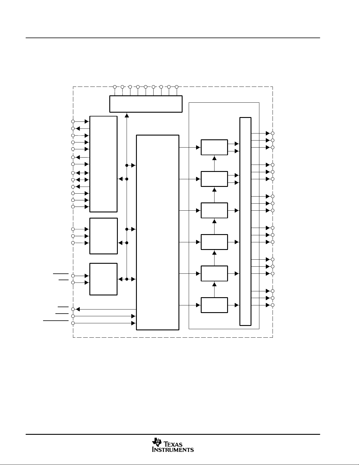
1.2 Functional Block Diagram
AVDD_PLL
AVSS_PLL
VREGA_CAP
VREGB_CAP
VREGC_CAP
DVDD_RCL
DVSS_RCL
DVDD_PWM
DVSS_PWM
MCLK_IN
XTAL_OUT
XTAL_IN
CSS
M_S
PLL_FLT_OUT
PLL_FLT_RET
SCLK
LRCLK
MCLKOUT
SDIN1
SDIN2
SDIN3
SDA
SCL
CSO
RESET
PDN
CLIP
MUTE
ERR_RCVY
Clock,
PLL
and
Serial
Data
I/F
Serial
Control
I/F
Reset,
Pwr Dwn
and
Status
Power Supply
Signal
Processing
Auto Mute
De-emphasis
Soft Volume
Error Recovery
Soft Mute
Clip Detect
PWM
Section
PWM Ch.
PWM Ch.
PWM Ch.
PWM Ch.
PWM Ch.
PWM Ch.
Output Control
PWM_AP_1
PWM_AM_1
Valid_1
PWM_AP_2
PWM_AM_2
Valid_2
PWM AP_3
PWM AM_3
Valid_3
PWM_AP_4
PWM_AM_4
Valid_4
PWM_AP_5
PWM_AM_5
Valid_5
PWM_AP_6
PWM_AM_6
Valid_6
2
SLES041B—November 2002TAS5026
Page 8
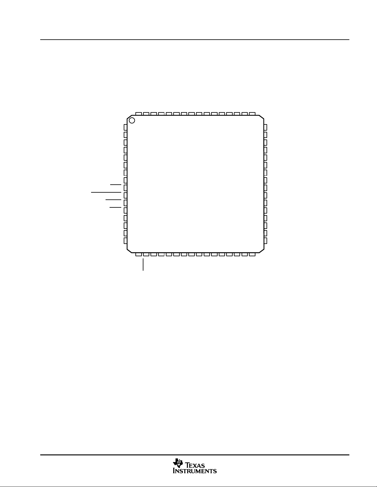
1.3 Terminal Assignments
1
NC
NC
2
3
4
5
6
7
8
9
10
11
12
13
14
15
16
MCLK_IN
AVDD_PLL
PLL_FLT_OUT
PLL_FLT_RET
AVSS_PLL
DVSS1
RST
ERR_RCVY
MUTE
PDN
SDA
SCL
CS0
DVSS1
PAG PACKAGE
(TOP VIEW)
AVDD_OSC
XTL_IN
XTL_OUT
AVSS_OSC
DVSS
PWM_AP_1
PWM_AM_1
VALID_1
PWM_AP_2
PWM_AM_2
VALID_2
PWM_AP_3
PWM_AM_3
VALID_3NCNC
64 63 62 61 60 59 58 57 56 55 54 53 52 51 50 49
17
18 19 21 22 23 24 25 26 27 28 29 30 31 32
20
48
47
46
45
44
43
42
41
40
39
38
37
36
35
34
33
Introduction
DVDD_RCL
DVSS_RCL
NC
DVDD_PWM
DVSS_PWM
PWM_AP_4
PWM_AM_4
VALID_4
PWM_AP_5
PWM_AM_5
VALID_5
PWM_AP_6
PWM_AM_6
VALID_6
NC
NC
CLIP
DBSPD
SDIN1
SDIN2
SCLK
SDIN3
MCLK_OUT
DVDD
LRCLK
NC
DVSS1
M_S
DVSS1
DEM_SEL2
DEM_SEL1
DVSS1
SLES041B—November 2002 TAS5026
3
Page 9
Introduction
1.4 Ordering Information
T exas Instruments
Audio Solutions
Device Number
T emperature Range
Package T ype
T AS
AVAILABLE OPTIONS
PACKAGE
T
A
0°C to 70°C TAS5026CPAG
–40°C to 85°C TAS5026IPAG
PLASTIC 64-PIN TQFP
(PAG)
5026 C PAG
1.5 Terminal Functions
TERMINAL
NAME NO.
AVDD_OSC 64 PWR Analog power supply for internal oscillator cells
AVDD_PLL 3 PWR 3.3-V analog power supply for PLL
AVSS_OSC 61 AOUT Analog ground for internal oscillator cells
AVSS_PLL 6 PWR Analog ground for PLL
CLIP 18 O Digital clipping indicator, active low
CS0 15 I I2C device address select. This is an active high pin.
DBSPD 17 I Sample rate is double speed (88.2 kHz or 96 kHz), active high
DM_SEL1 29 I De-emphasis select bit 1 (0 = none, 01 = 32 kHz, 10 = 44.1 kHz
DM_SEL2 28 I De-emphasis select bit 2, 10 = 48 kHz, 11= undefined (none)
DVDD_PWM 45 PWR 3.3-V digital power supply for PWM
DVDD_RCL 48 PWR 3.3-V digital power supply for re-clocker
DVDD 25 PWR 3.3-V digital power supply for digital core and most of I/O buffers
DVSS 60 I Voltage regulator enable, active low
DVSS_PWM 44 PWR Digital ground for PWM
DVSS_RCL 47 PWR Digital ground for re-clocker
DVSS1 8, 26,
31, 32
ERR_RCVY 10 I Error recovery, active low
LRCLK 24 I/O Serial audio data left / right clock (sampling rate clock) (input when M_S = 0; output when M_S
M_S 30 I Master/slave mode input signal (master = 1, slave = 0)
MCLK_IN 2 I MCLK input, slave mode
MCLK_OUT 22 O MCLK output buffered system clock output M_S = 1; otherwise set to 0
I/O
PWR Digital ground for digital core and most of I/O buffers
= 1)
DESCRIPTION
4
SLES041B—November 2002TAS5026
Page 10
Introduction
TERMINAL
NAME
MUTE 11 I Mute input signal, active low
NC 1, 7,
PDN 12 I Power down. This signal is active low.
PLL_FLT_OUT 4 I PLL external filter
PLL_FLT_RET 5 I PLL external filter
PWM_AM_1 58 O PWM 1 output (differential -); {Positive H-bridge side}
PWM_AM_2 55 O PWM 2 output (differential -); {Positive H-bridge side}
PWM_AM_3 52 O PWM 3 output (differential -); {Positive H-bridge side}
PWM_AM_4 42 O PWM 4 output (differential -); {Positive H-bridge side}
PWM_AM_5 39 O PWM 5 output (differential -); {Positive H-bridge side}
PWM_AM_6 36 O PWM 6 output (differential -); {Positive H-bridge side}
PWM_AP_1 59 O PWM 1 output (differential +); {Positive H-bridge side}
PWM_AP_2 56 O PWM 2 output (differential +); {Positive H-bridge side}
PWM_AP_3 53 O PWM 3 output (differential +); {Positive H-bridge side}
PWM_AP_4 43 O PWM 4 output (differential +); {Positive H-bridge side}
PWM_AP_5 40 O PWM 5 output (differential +); {Positive H-bridge side}
PWM_AP_6 37 O PWM 6 output (differential +); {Positive H-bridge side}
RST 9 I System reset input. This signal is an active low.
SCL 14 I I2C clock signal
SCLK 23 I/O Serial audio data clock (master mode = output, slave mode = input)
SDA 13 I/O I2C data signal
SDIN1 19 I Serial audio data 1 input
SDIN2 20 I Serial audio data 2 input
SDIN3 21 I Serial audio data 3 input
VALID_1 57 O Output indicating validity of PWM outputs, channel 1, active high
VALID_2 54 O Output indicating validity of PWM outputs, channel 2, active high
VALID_3 51 O Output indicating validity of PWM outputs, channel 3, active high
VALID_4 41 O Output indicating validity of PWM outputs, channel 4, active high
VALID_5 38 O Output indicating validity of PWM outputs, channel 5, active high
VALID_6 35 O Output indicating validity of PWM outputs, channel 6, active high
XTL_IN 63 AIN Crystal or TTL level clock input
XTL_OUT 62 AOUT Crystal output (not for external usage)
NO.
No connection
27, 49,
50
DESCRIPTIONI/O
DESCRIPTIONI/O
SLES041B—November 2002 TAS5026
5
Page 11

Architecture Overview
2 Architecture Overview
The T AS5026 is composed of six functional elements:
• Clock, PLL, and serial data interface (IIS)
• Reset/power down circuitry
• Serial control interface (IIC)
• Signal processing unit
• Pulse width modulator (PWM)
• Power supply
2.1 Clock and Serial Data Interface
The T AS5026 clock and serial data interface contains an input serial data slave and the clock master/ slave
interface.
The serial data slave interface receives information from a digital source such as a DSP, S/PDIF receiver,
analog-to-digital converter (ADC), digital audio processor (DAP) such as the TAS3103, or other serial bus
master at sample rates of for sample rates of 32 kHz, 44.1 kHz, 48 kHz, 88.2 kHz, 96 kHz,176.4 kHz, and 192
kHz. The serial data interface has three serial data inputs that can accept up to six channels of data. The serial
data interfaces support left justified and right justified for 16-, 20-, and 24-bits. In addition, the serial data
interfaces support the DSP protocol for 16 bits and the I2S protocal for 24 bits. The received data is data
passed to the TAS5026 signal-processing unit.
The T AS5026 can function as a receiver or a generator for the MCLK_IN (master clock), SCLK (shift clock),
and LRCLK (left/right clock) signals that control the flow of data on the three serial data interfaces. The
T AS5026 is a clock master when it generates these clocks and is a clock slave when it receives these clocks.
The T AS5026 is a synchronous design that relies upon master clock to provide a reference clock for all of the
device operations. When operating as a slave, this reference clock is MCLK_IN. When operating as a master,
the reference clock is either TTL clock input to XT AL_IN or a crystal attached across XTAL_IN and XT AL_OUT .
If the master clock stops, the T AS5026 will perform a clock error recovery sequence. The clock error recovery
sequence temporarily suspends processing, places the PWM outputs in a hard mute (PWM_P outputs are
low; PWM_M outputs are high, and all VALID signals are low), resets all internal processes, sets the volumes
to mute, and suspends all I
When the master clock is resumed, the TAS5026 exits the clock error recovery sequence by performing a
4.3-ms partial re-initialization, noiselessly restarting the PWM output, and ramping the volume up to the level
specified in the volume control registers. The volume update is performed over a 43-ms. interval. The
TAS5026 preserves all control register settings that were set prior to the clock interruption.
If a clock error occurs while the ERR_RCVRY pin is asserted (LOW), the TAS5026 will perform the error
recovery sequence up to the unmute sequence. In this case, the volume remains at full attenuation with the
PWM output at a 50% duty cycle. The volume can be restored from this state by triggering a mute/unmute
sequence via the mute pin LOW then HIGH.
The clock and serial data interface has two control parameters: data sample rate and clock master or slave.
2
C operations.
2.1.1 Normal-Speed, Double-Speed, and Quad-Speed Selection
The sampling rate is selected through a pin (DBSPD) or the serial control register 0 (X02). When a sample
rate is selected, the system automatically performs an error recovery sequence and switches to the new
sampling rate. As shown in subsequent sections, the sample rate control sets the frequencies of the SCLK
and LRCLK in clock slave mode and the output frequencies of SCLK and LRCLK in clock master mode.
During the error recovery sequence, the T AS5026 temporarily suspends processing, places the PWM outputs
in a hard mute (PWM P outputs LOW; PWM M outputs HIGH, and all VALID signals LOW), resets all internal
processes, and suspends all I
noiselessly restarts the PWM output. The T AS5026 preserves all control register settings through out the error
recovery sequence.
6
2
C operations. The T AS5026 then performs a 4.3-ms partial re-initialization and
SLES041B—November 2002TAS5026
Page 12
Architecture Overview
There are three data rates: normal speed, double speed, and quad speed.
Normal-speed mode supports data rates of 32 kHz, 44.1 kHz, and 48 kHz. Normal speed is supported in the
master and slave modes. The PWM is placed in normal speed by setting the DBSPD terminal low or by setting
the normal mode bits in the system control register through the serial control interface. Following this
operation, the PWM performs an error recovery sequence automatically and operates in the normal speed
mode.
Double-speed mode is used to support sampling rates of 88.2 kHz and 96 kHz. Double speed is supported
in master and slave modes. The PWM is placed in double speed mode by setting the DBSPD terminal high
or by setting the double speed bits in the system control register through the serial control interface. Following
this operation, the PWM performs an error recovery sequence automatically and operate in double speed
mode.
Quad-speed mode is used to support sampling rates of 176.4 kHz and 192 kHz. Quad-speed mode is auto
detected supported in slave mode and invoked by control in master mode in slave mode, if the device is not
in double speed mode, quad-speed mode is automatically detected when MCLK_IN is 128Fs. In master mode,
the PWM is placed in quad-speed mode by setting the quad-speed bit in the system control register through
the serial control interface.
Table 2–1. Normal-Speed, Double-Speed, and Quad-Speed Operation
QUAD-SPEED CONTROL
REGISTER BIT
0 0 Master or slave Normal speed
0 1 Master or slave Double speed
1 0 Master or slave Quad speed
0 0 Slave Quad speed if MCLK_IN = 128Fs
1 1 Master or slave Error
DBSPD TERMINAL OR
CONTROL REGISTER BIT
MODE SPEED SELECTION
2.1.2 Clock Master/Slave Mode (M_S)
Clock master and slave mode can be invoked using the M_S (master slave) terminal.
This terminal specifies the default mode that is set immediately following a device RESET. The serial data
interface setting permits the clock generation mode to be changed during normal operation.
The transition to master mode occurs:
• Following a RESET when M_S terminal has a logic high applied
The transition to slave mode occurs:
• Following a RESET when M_S terminal has a logic low applied
2.1.3 Clock Master Mode
When M_S = 1 following a RESET, the T AS5026 provides the master clock, SCLK, and LRCLK to the rest of
the system. In the master mode, the TAS5026 outputs the audio system clocks MCLK_OUT, SCLK, and
LRCLK.
The T AS5026 device generates these clocks plus its internal clocks from the internal phase-locked loop (PLL).
The reference clock for the PLL can be provided by either an external clock source (attached to XT AL_IN) or
a crystal (connected across terminals XT AL_IN and XT AL_OUT). The external source attached to MCLK_IN
is 256 times (128 in quad mode) the data sample rate (Fs). The SCLK frequency is 64 times the data sample
rate and the SCLK frequency of 48 times the data sample rate is not supported in the master mode. The LRCLK
frequency is the data sample rate.
2.1.3.1 Crystal Type and Circuit
In clock master mode the T AS5026 can derive the MCLKOUT , SCLK, and LRCLK from a crystal. In this case,
the TAS5026 uses a parallel-mode fundamental-mode crystal. This crystal is connected to the TAS5026 as
shown in Figure 2–1.
SLES041B—November 2002 TAS5026
7
Page 13
Architecture Overview
TAS5026
rd = Drive level control resistor – crystal vendor specified
CL = Crystal load capacitance (capacitance of circuitry between the two terminals of the crystal)
CL = (C1 x C2 )/(C1 + C2 ) + CS (where CS = board stray capacitance ~ 3 pF)
Example: Vendor recommended CL = 18 pF, CS = 3 pF ≥ C1 = C2 = 2 x (18–3) = 30 pF
2.1.4 Clock Slave Mode
In the slave mode (M_S = 0), the master clock, LRCLK, and SCLK are inputs to the T AS5026. The master clock
is supplied through the MCLK_IN terminal.
C
1
C
2
r
d
OSC
MACRO
XO
XI
AVSS
Figure 2–1. Crystal Circuit
As in the master mode, the TAS5026 device developed its internal timing from internal phase-locked loop
(PLL). The reference clock for the PLL is provided by the input to the MCLK_IN terminal. This input is at a
frequency of 256 times (128 in quad mode) the input data rate. The SCLK frequency is 48 or 64 times the data
sample rate. The LRCLK frequency is the data sample rate. The T AS5026 does not require any specific phase
relationship between SRCLK and MCLK_IN, but there must be synchronization.
The TAS5026 monitors the relationship between MCLK, SCLK and LRCLK. The TAS5026 detects if any of
the three clocks are absent, if LRCLK rate changes more the ±10 MCLK cycles since the last device reset or
clock error recovery , or if MCLK frequency is changing substantially with respect to the PLL frequency . When
a clock error is detected the T AS5026 performs a clock error recovery sequence. If one or more of the clock
signals are absent, the TAS5026 is held with the outputs in hard mute until the clock is resumed. Once the
clock is resumed, the clock error recover sequence is completed.
NOTE:
The detection of a clock error causes the TAS5026 to perform an immediate hard mute and
suspension of all processes. This abrupt transition can produce a faint click as the outputs are
muted.
Since the clocks are removed when changing media or during input selection, it is possible to use this
knowledge to completely eliminate clicks in these conditions. In this case, the click is prevented by muting the
outputs by using the MUTE
terminal or the I2C /MUTE command 43 ms in advance of the clocks being
removed.
In the slave mode, MCLK_OUT is driven low.
Table 2–2 shows all the possible master and slave modes. When operating in quad mode (Fs = 176.4 kHz
or 192 kHz), the device works in slave mode only with MCLK_IN = 128 Fs.
Table 2–3 shows the clocks speed for normal, double and quad modes.
8
SLES041B—November 2002TAS5026
Page 14
Architecture Overview
Table 2–2. Master and Slave Clock Modes
DESCRIPTION M_S DBSPD
Internal PLL, master, normal speed 1 0 8.192 - 2.048 32 8.192
Internal PLL, master, normal speed 1 0 11.2896 - 2.8224 44.1 11.2896
Internal PLL, master, normal speed 1 0 12.288 - 3.072 48 12.288
Internal PLL, master, double speed 1 1 - 22.5792
Internal PLL, master, double speed 1 1 - 24.576
Internal PLL, master, quad speed 1 0 - 22.5792 11.2896 176.4 22.5792
Internal PLL, master, quad speed 1 0 - 24.576 12.288 192 24.576
Internal PLL, slave, normal speed 0 0 - 8.192§ 2.0484 32 Digital GND
Internal PLL, slave, normal speed 0 0 - 11.2896
Internal PLL, slave, normal speed 0 0 - 12.288§ 3.072 48 Digital GND
Internal PLL, slave, double speed 0 1 - 22.5792 5.6448 88.2 Digital GND
Internal PLL, slave, double speed 0 1 - 24.576§ 6.144 96 Digital GND
Internal PLL, slave, quad speed
Internal PLL, slave, quad speed
External PLL, master, normal speed 1 0 - - 2.048 32 8.192
External PLL, master, normal speed 1 0 - - 2.8224 44.1 11.2896
External PLL, master, normal speed 1 0 - - 3.072 48 12.288
External PLL, master, double speed 1 1 - - 5.6448 88.2 22.5792
External PLL, master, double speed 1 1 - - 6.144 96 24.576
External PLL, master, quad speed 1 0 - - 11.2896 176.4 22.5792
External PLL, master, quad speed 1 0 - - 12.288 192 24.576
External PLL, slave, normal speed 0 0 - 8.192§ 2.0484 32 Digital GND
External PLL, slave, normal speed 0 0 - 11.2896
External PLL, slave, normal speed 0 0 - 12.288§ 3.072 48 Digital GND
External PLL, slave, double speed 0 1 - 22.5792 5.6448 88.2 Digital GND
External PLL, slave, double speed 0 1 - 24.576§ 6.144 96 Digital GND
External PLL, slave, quad speed
External PLL, slave, quad speed
†
A crystal oscillator is connected to XTL_IN.
‡
MCLK_IN tied low when input to XTL_IN is provided; XTL_IN tied low when MCLK_IN_IN is provided.
§
External MCLK_IN connected to MCLK_IN_IN input
¶
SCLK and LRCLK are outputs when M_S=1, and inputs when M_S=0.
#
MCLK_OUT is driven low when M_S=0.
||
Quad-speed mode is detected automatically.
||
||
||
||
0 0 - 22.5792
0 0 - 24.576§ 12.288 192 Digital GND
0 0 - 22.5792
0 0 - 24.576§ 12.288 192 Digital GND
XTL_IN
(MHz)
k SCLK can be 48 or 64 times Fs
†
MCLK_IN
‡
(MHz)
SCLK
¶
(MHz)
§
§
§
§
§
§
5.6448 88.2 22.5792
6.144 96 24.576
2.8224 44.1 Digital GND
11.2896 176 Digital GND
2.8224 44.1 Digital GND
11.2896 176 Digital GND
LRCLK
(kHz)
¶
MCLK_OUT
(MHz)
#
Table 2–3. LRCLK, MCLK_IN, and External PLL Rates
NORMAL SPEED (kHz) DOUBLE SPEED (kHz) QUAD SPEED (kHz)
LRCLK 1FS 32 44.1 48 1FS 64 88.2 96 1FS 176.4 192
MCLK_IN 256FS 8,192 11,289.6 12,288 256FS 16,384 22,579.2 24,576 128FS 22,579.2 24,576
EXT. PLL 2048FS 65,536 90,316.8 98,304 1024FS 65,536 90,316.8 98,304 512FS 90,316.8 98,304
SLES041B—November 2002 TAS5026
9
Page 15
Architecture Overview
2.1.5 PLL Filter
A low jitter PLL produces the internal timing of the T AS5026 (when in master mode), the master clock, SCLK,
and LRCLK. Connections for the PLL external loop filter are provided through PLL_FLT_OUT and
PLL_FLT_RET as shown in Figure 2–2.
PLL_FLT_OUT
220 Ω
2.1.6 DCLK
DCLK is the internal high frequency clock that is produced by the PLL circuitry from MCLK. The T AS5026 uses
the DCLK to control all internal operations. DCLK is 8 times the speed of MCLK in normal speed mode, 4 times
MCLK in double speed, and 2 times MCLK in quad speed. With respect to the I
clock cycles are used to specify Interchannel delay and to detect when the MCLK is frequency is drifting.
Table 2–4 DCLK shows the relationship between Sample Rate, MCLK and DCLK.
TAS5026
47 nF
PLL_FLT_RET
4.7 nF
Figure 2–2. External PLL Loop Filter
2
C addressable registers, DCLK
Table 2–4. DCLK
FS
(kHz)
32 8.1920 65.5360 15.3
44.1 11.2896 90.3168 11.1
48 12.2880 98.3040 10.2
88 22.5280 90.1120 11.1
96 24.5760 98.3040 10.2
192 49.1520 98.3040 10.2
MCLK
(MHz)
DCLK
(MHz)
DCK Period
(ns)
2.1.7 Serial Data Interface
The T AS5026 operates as a slave only/receive only serial data interface in all modes. The TAS5026 has three
PCM serial data interfaces to accept six channels of digital data though the SDIN1, SDIN2, SDIN3 inputs. The
serial audio data is in MSB first; 2’s complement format.
The serial data interfaces of the T AS5026 can be configured in right justified, I
This interface supports 32-kHz, 44.1-kHz, 48-kHz, 88-kHz, 96-kHz, 176.4-kHz, and 192-kHz data sample
rates. The serial data interface format is specified using the data interface control register. The supported word
lengths are shown in Table 2–5.
During normal operating conditions if the serial data interface settings change state, an error recovery
sequence is initiated.
10
2
S, left-justified, or DSP modes.
SLES041B—November 2002TAS5026
Page 16
DATA MODES
Right justified, MSB first 16 0 0 0
Right justified, MSB first 20 0 0 1
Right justified, MSB first 24 0 1 0
I2S 16 0 1 1
I2S 20 1 0 0
I2S 24 1 0 1
Left justified, MSB first 24 1 1 0
DSP frame 16 1 1 1
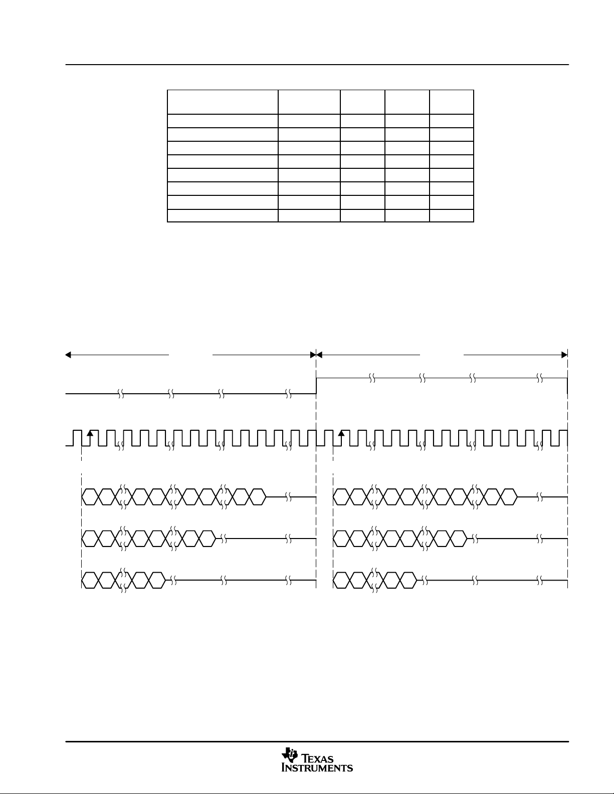
2.1.7.1 I2S Timing
I2S timing uses an LRCLK to define when the data being transmitted is for the left channel and when it is for
the right channel. The LRCLK is low for the left channel and high for the right channel. A bit clock running at
48 or 64 times Fs is used to clock in the data. There is a delay of one bit clock from the time the LRCLK signal
changes state to the first bit of data on the data lines. The data is written MSB first and is valid on the rising
edge of the bit clock. The T AS5026 masks unused trailing data bit positions. Master mode only supports a 64
times Fs bit clock.
2-Channel I2S (Philips Format) Stereo Input
32 Clks
Table 2–5. Supported Word Lengths
WORD
LENGTHS
MOD2 MOD1 MOD0
Architecture Overview
32 Clks
LRCLK (Note Reversed Phase) Left Channel
SCLK
MSB LSB
24-Bit Mode
23 22
20-Bit Mode
19 18
16-Bit Mode
9 8 5 4 1 0
5 4 1 0
1 015 14
Figure 2–3. I2S 64-Fs Format
Right Channel
SCLK
MSB LSB
23 22
19 18 5 4 1 0
9 8 5 4 1 0
1 015 14
SLES041B—November 2002 TAS5026
11
Page 17
Architecture Overview
2
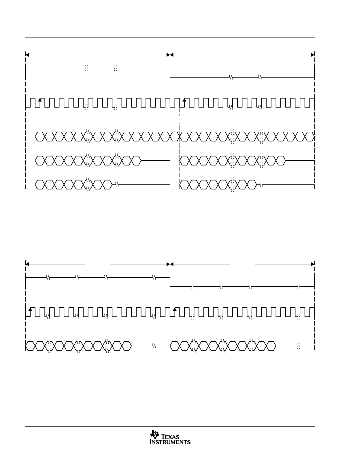
2-Channel I2S Stereo Input/Output (24-Bit Transfer Word Size)
24 Clks
LRCLK
Left Channel
24 Clks
Right Channel
SCLK
MSB LSB
24-Bit Mode
22
23
20-Bit Mode
19 18
16-Bit Mode
20 19 8 7 2 1
16 15 1 0
12
11
13
4
517
1 015 14
4 3521
Figure 2–4. I2S 48-Fs Format
2.1.7.2 Left-Justified Timing
Left-justified (LJ) timing uses an LRCLK to define when the data being transmitted is for the left channel and
when it is for the right channel. The LRCLK is high for the left channel and low for the right channel. A bit clock
running at 48 or 64 times Fs is used to clock in the data. The first bit of data appears on the data lines at the
same time the LRCLK toggles. The data is written MSB first and is valid on the rising edge of the bit clock.
The TAS5026 masks unused trailing data bit positions. Master mode only supports a 64 times Fs bit clock.
-Channel Left-Justified Stereo Input
32 Clks
LRCLK
Left Channel
SCLK
MSB LSB
23 22
0
19 18 16 15 1 0
LRCLK
20 19 8 7 2 1
4
517
12
11
1 015 14
32 Clks
Right Channel
13
4 3521
SCLK
MSB LSB
24-Bit Mode
23 22
NOTE: All data presented in 2s complement form with MSB first.
9 8 5 4 1 0
MSB LSB
23
22
9 8 5 4 1 0
Figure 2–5. Left-Justified 64-Fs Format
12
SLES041B—November 2002TAS5026
Page 18
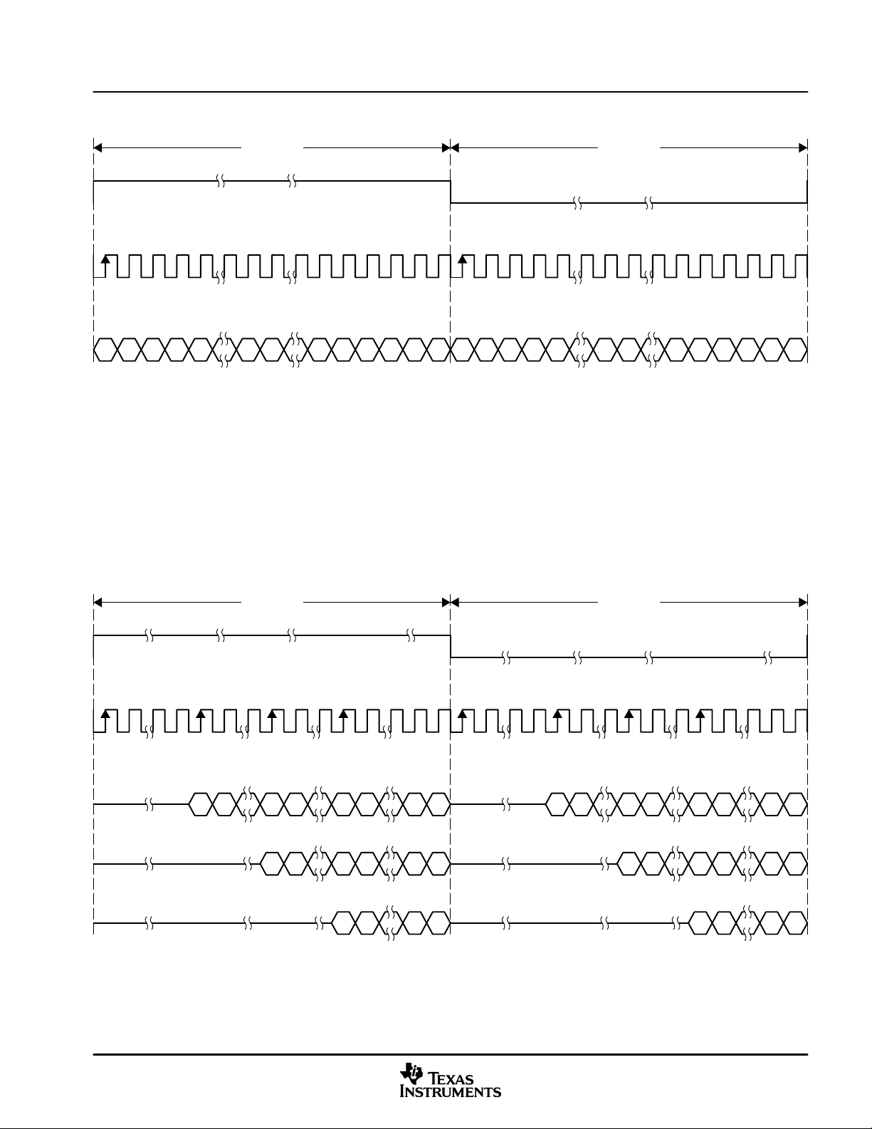
2-Channel Left-Justified Stereo Input/Output (24-Bit Transfer Word Size)
Architecture Overview
24 Clks
LRCLK
Left Channel
SCLK
MSB LSB
24-Bit Mode
22
21
19 9 8 1 0
3 242023 22 21
Figure 2–6. Left-Justified 48-Fs Format
2.1.7.3 Right-Justified Timing
Right-justified (RJ) timing uses an LRCLK to define when the data being transmitted is for the left channel and
when it is for the right channel. The LRCLK is high for the left channel and low for the right channel. A bit clock
running at 48 or 64 times Fs is used to clock in the data. The first bit of data appears on the data 8-bit clock
periods (for 24-bit data) after LRCLK toggles. In RJ mode, the last bit clock before LRCLK transitions always
clocks the LSB of data. The data is written MSB first and is valid on the rising edge of bit clock. The T AS5026
masks unused leading data bit positions. Master mode only supports a 64 times Fs bit clock.
2-Channel Right-Justified (Sony Format) Stereo Input
24 Clks
Right Channel
MSB LSB
19 9 8 1 0
5
3 2420235
32 Clks
LRCLK
Left Channel
SCLK
MSB LSB
24-Bit Mode
23 22
20-Bit Mode
16-Bit Mode
NOTE: All data presented in 2s complement form with MSB first.
19 18 15 14 1 0
19 18
15 14 1 0
1 015 14
Figure 2–7. Right-Justified 64-Fs Format
32 Clks
Right Channel
MSB LSB
23 22
19 18 15 14 1 0
19 18 15 14 1 0
1 015 14
SLES041B—November 2002 TAS5026
13
Page 19

Architecture Overview
2-Channel Right-Justified Stereo Input/Output (24-Bit Transfer Word Size)
24 Clks
LRCLK
Left Channel
SCLK
MSB LSB
24-Bit Mode
22
21
20-Bit Mode
16-Bit Mode
NOTE: All data presented in 2s complement form with MSB first.
19 1 0
2023
18
18 89
19 1 0
15 14 22 21
15 14
89
8915 14
1 0
Figure 2–8. Right-Justified 48-Fs Format
24 Clks
Right Channel
MSB LSB
19 1 0
2023
18
18 89
19 1 0
15 14
15 14
89
8915 14
1 0
2.1.7.4 DSP Mode Timing
DSP mode timing uses an LRCLK to define when data is to be transmitted for both channels. A bit clock running
at 64 × Fs is used to clock in the data. The first bit of the left channel data appears on the data lines following
the LRCLK transition. The data is written MSB first and is valid on the rising edge of the bit clock. The T AS5026
masks unused trailing data bit positions.
SCLK
LRCLK
SDIN
16 Bits
Left
Channel
64 SCLKS
LSBMSB
16 Bits
Right
Channel
LSBMSB
32 Bits Unused
14
Figure 2–9. DSP Format
SLES041B—November 2002TAS5026
Page 20

2.2 Reset, Power Down, and Status
The reset, power down, and status circuitry provides the necessary controls to bring the T AS5026 to the initial
inactive condition, achieve low power standby, and report system status.
2.2.1 Reset—RESET
The T AS5026 is placed in the reset mode by setting the RESET terminal low.
Architecture Overview
RESET
is an asynchronous control signal that restores the TAS5026 to its default conditions, sets the valid
1–6 outputs low, and places the PWM in the hard mute state. Volume is immediately set to full attenuation
(there is no ramp down).
As long as the RESET
bus operations are ignored. Table 2–6 shows the device output signals while RESET
Upon the release of RESET
terminal is held low, the device is in the reset state. During reset, all I2C and serial data
is active.
, if POWER_DWN is high, the system performs a 4-ms to 5-ms device initialization
and then ramps the volume up to 0 db using a soft volume update sequence. If MCLK_IN is not active when
RESET is released high, then a 4-ms to 5-ms initialization sequence is produced once MCLK_IN becomes
active.
During device initialization all controls are reset to their initial states. T able 2–7 shows the control settings that
are changed during initialization.
RESET
should be applied during power-up initialization or while changing the master slave clock states.
Table 2–6. Device Outputs During Reset
SIGNAL MODE SIGNAL STATE
Valid 1–Valid 6 All Low
PWM P-outputs All Low
PWM M-outputs All Low
MCLKOUT All Low
SCLK Master Low
SCLK Slave Signal input
LRCLK Master Low
LRCLK Slave Signal input
SDA All Signal input
CLIP All High
Because the RESET is an asynchronous control signal, small clicks and pops can be produced during the
application (the leading edge) of this control. However, when RESET
is released, the transition from the hard
mute state back to normal operation is performed synchronously using a quiet sequence.
If a completely quiet reset sequence is desired, MUTE
should be applied before applying RESET.
Table 2–7. Values Set During Reset
CONTROL SETTING
Volume 0 dB
MCLK_IN frequency 256
Master/slave mode M_S terminal state
Auto mute Enabled
De-emphasis None
DC offset 0
Interchannel delay Each channel set at 16 clocks higher then preceding channel
SLES041B—November 2002 TAS5026
15
Page 21

Architecture Overview
2.2.2 Power Down—PDN
The T AS5026 can be placed into the power-down mode by holding the PDN terminal low . When power-down
mode is entered, both the PLL and the oscillator are shut down. Volume is immediately set to full attenuation
(there is no ramp down). The valid 1–6 outputs are immediately asserted low and the PWM outputs are placed
in the hard mute state. PDN
is held low—the device is in the power-down (hard mute) state.
During power down, all I
signals while PDN
To place the device in total power-down mode, both RESET and power-down modes must be enabled. Prior
to bringing PDN
Because PDN is an asynchronous control signal, small clicks and pops can be produced during the application
(the leading edge) of this control. However, when PDN
to normal operation is performed synchronously using a quiet sequence.
If a completely quiet reset sequence is desired, MUTE
is active.
high, RESET must be brought low for a minimum of 50 ns.
initiates device power down without clock inputs. As long as the PDN terminal
2
C and serial data bus operations are ignored. Table 2–8 shows the device output
Table 2–8. Device Outputs During Power Down
SIGNAL MODE SIGNAL STATE
Valid 1–Valid 6 All Low
PWM P-outputs All Low
PWM M-outputs All Low
MCLKOUT All Low
SCLK Master Low
SCLK Slave Signal input
LRCLK Master Low
LRCLK Slave Signal input
SDA All Signal input
CLIP All High
is released, the transition from the hard mute state back
should be applied before applying PDN.
2.2.2.1 Recovery Time Options
T o support the requirements of various system configurations, the TAS5026 can come up to the normal state
after either a long (100 ms) or a short (5 ms) delay.
1. In the first case, a slow system (95 ms to 100 ms) start-up occurs at the end of the power-down sequence
when:
RESET
is high for at least 16 MCLK_IN periods before PDN goes high.
2. Otherwise a fast (4 ms to 5 ms) start up occurs.
NOTE: If MCLK_IN is not active when both of these signals are released high, then a a fast
(4 ms to 5 ms) start up occurs once MCLK_IN becomes active.
2.2.3 Status Registers
The T AS5026 provides device identification and operational status information that is accessible through the
serial control interface status registers that provide general device information.
Device ID—The T AS5026 provides a device identification code that is accessible through the serial control
interface
Volume Update is in Progress—Whenever a volume change is in progress, this status bit is high.
No Internal Errors (All Valid Signals are High)—When there are no internal errors in the TAS5026 and all
outputs are valid, this status bit is high.
LRCLK Error—When there are the MCLK_IN rate changes more than ±10 MCLK_IN cycles from the correct
number of cycles (128 or 256) per LRCLK cycle
MCLK_IN Error—When the MCLK_IN frequency changes such that it is out of synchronization with internal
PLL generated clock
16
SLES041B—November 2002TAS5026
Page 22

2.3 Signal Processing
This section contains the signal processing functions that are contained in the TAS5026. The signal
processing is performed using a high-speed 24-bit signal processing architecture. The T AS5026 performs the
following signal processing features:
• Individual channel soft volume with a range of 24 dB to –114 dB plus mute
• Soft mute
• Auto mute
• 50-µs/15-µs de-emphasis filter supported in the sampling rates 32 kHz, 44.1 kHz, and 48 kHz
2.3.1 Volume Control
The gain of each output can be adjusted by a soft digital volume control for each channel. Volume adjustments
are performed using a soft gain update s-curve, which is approximated using a second order filter fit. The curve
fit is performed over a transition interval between 41 ms and 65 ms.
The volume of each channel can be adjusted from mute to 24 dB to –1 14 dB in 0.5 dB steps. Because of the
numerical representation that is used to control the volume, at very low volume levels the step size increases
for gains of that are less than –96 dB. The default volume setting following power up or reset is 0 dB for all
channels. The step size increases linearly up to approximately –90 dB, see Figure 2–10.
6.0
5.5
5.0
4.5
4.0
3.5
3.0
2.5
Step Size – dB
2.0
1.5
1.0
0.5
0.0
–110 –100 –90 –80 –70 –60 –50 –40 –30 –20 –10 0 10 20
Architecture Overview
STEP SIZE
vs
ATTENUATION (GAIN)
Attenuation (Gain) – dB
Figure 2–10. Attenuation Curve
The volume control format for each channel is expressed in 8 bits. The volume for each channel is set by writing
8 bits via the serial control interface. The MSB bit is written first as in the bit position 0 (LSB position).
The volume for each channel can be set using a single or multiple address write operation to the volume control
register via the serial control interface. To change the volume of all six channels requires that 6 registers be
updated.
To coordinate the volume adjustment of multiple channels simultaneously , the TAS5026 performs a delayed
volume update upon receiving a volume change command. Following the completion of the register volume
write operations, the T AS5026 waits for 5 ms for another volume command to be given. If no volume command
is issued in that period of time, the T AS5026 starts adjusting the volume of the channels that received volume
settings.
SLES041B—November 2002 TAS5026
17
Page 23

Architecture Overview
While a volume update is being performed, the system status register indicates that the update is in progress.
During the update, all subsequent volume control setting requests that are sent to the T AS5026 are received
and stored as a single next value for a subsequent update. If more than one volume setting request is sent,
only the last is retained.
Table 2–9. V olume Register
VOLUME REGISTER
D 7 D 6 D 5 D 4 D 3 D 2 D 1 D 0
Vol
Bit 7
Vol
Bit 6
Vol
Bit 5
Vol
Bit 4
Vol
Bit 3
Vol
Bit 2
Vol
Bit 1
2.3.2 Mute
The application of mute ramps the volume from any setting to noiseless hard mute state. There are two
methods in which the T AS5026 can be placed into mute. The T AS5026 is placed in the noiseless mute when
the MUTE
initiated by setting the mute bit in the system control register through the serial control interface. The T AS5026
is held in mute state as long as the terminal is low or I
and exit sequences to and from the hard mute state.
If an error recovery (described in the PWM section) occurs after a mute request has been received, the device
returns from error recovery with the channel volume set as specified by the mute command.
terminal is asserted low for a minimum of 3 MCLK_IN cycles. Alternatively , the mute mode can be
2
C mute setting is active. This command uses quiet entry
Vol
Bit 0
2.3.3 Auto Mute
Auto mute is an automatic sequence that can be enabled or disabled via the serial control interface. The
default for this control is enabled. When enabled, the PWM auto mutes an individual channel when a channel
receives from 5 ms to 50 ms of consecutive zeros. This time interval can be selectable using the auto mute
delay register. The default interval is 5 ms at 48 kHz. This duration is independent of the sample rate. The auto
mute state is exited when two consecutive samples of nonzero data are received.
This mode uses the valid low to provide a low-noise floor while maintaining a short startup time. Noise free
entry and exit is achieved by using the PWM quiet start and stop sequences.
2.3.4 Individual Channel Mute
Individual channel mute is invoked through the serial interface. Individual channel mute permits each channel
of the T AS5026 to be individually muted and unmuted. The operation that is performed is identical to the mute
operation; however, it is performed on a per channel basis. A TAS5026 channel is held in the mute state as
long as the serial interface mute setting for that channel is set.
2.3.5 De-Emphasis Filter
For audio sources that have been pre-emphasized, a precision 50-µs/15-µs de-emphasis filter is provided to
support the sampling rates of 32 kHz, 44.1 kHz, and 48 kHz. See Figure 2–11 for a graph showing the
de-emphasis filtering characteristics. De-emphasis is set using two bits in the system control register.
Table 2–10. De-Emphasis Filter Characteristics
DEM_SEL2 (MSB) DEM_SEL1 DESCRIPTION
0 0 De-emphasis disabled
0 1 De-emphasis enabled for Fs = 48 kHz
1 0 De-emphasis enabled for Fs = 44 kHz
1 1 De-emphasis enabled for Fs = 32 kHz
18
Following the change of state of the de-emphasis bits, the PWM outputs go into the soft mute state. After 128
LRCLK periods for initialization, the PWM outputs are driven to the normal (unmuted) mode.
SLES041B—November 2002TAS5026
Page 24

0
–10
Response – dB
3.18 (50 µs) 10.6 (15 µs)
Figure 2–11. De-Emphasis Filter Characteristics
2.4 Pulse Width Modulator (PWM)
The T AS5026 contains six channels of high performance digital Equibit PWM modulators that are designed
to drive switching output stages (back ends) in both single-ended (SE) and H-bridge (bridge tied load)
configuration. The TAS5026 device uses noise shaping and sophisticated error correction algorithms to
achieve high power efficiency and high-performance digital audio reproduction.
The PWM provides six pseudo-differential outputs to drive six monolithic power stages (such as TAS5110)
or six discrete differential power stages using of gate drivers (such as the TAS5182) and MOSFETs in
single-ended or bridged configurations. The T AS5026 also provides a high performance differential output that
can be used to drive an external analog headphone amplifier.
Architecture Overview
De-Emphasis
f – Frequency – kHz
2.4.1 Clipping Indicator
The clipping output is designed to indicate clipping. When any of the six PWM outputs exceeds the maximum
allowable amplitude, the clipping indicator is asserted. The clipping indicator is cleared every 10 ms.
2.4.2 Error Recovery
Error recovery is used to provide error management and to permit the PWM output to be reset while preserving
all inter-volume, inter-channel delay , dc offsets, and the other internal settings. Error recovery is initiated by
bringing the ERR_RCVRY
in control register 1. Error recovery is a level sensitive signal.
The device also performs an error recovery automatically:
• When the speed configuration is changed to normal, double, or quad speed
• Following a change in the serial data bus interface configuration
When ERR_RCVRY
there are any pending speed configurations, these changes are then performed. When ERR_RCVRY
brought high, a delay of 4 ms to 5 ms is performed before the system starts the output re-initialization
sequence. After the initialization time, the TAS5026 begins normal operation. During error recovery, all
controls and device settings that were not updated are maintained in their current configurations.
To permit error recovery to be used to provide T AS5100 error management and recovery , the delay between
the start of (falling edge) error recovery and the falling edge of valid 1 though valid 6 is selectable. This delay
can be selected to be either 6 µs or 47 µs.
is brought low, all valid signals go low, and the PWM-P and PWM-M outputs go low. If
terminal low for a minimum 5 MCLK_IN cycles or by setting the error recovery bit
is
During error recovery all serial data bus operations are ignored. At the conclusion of the sequence, the error
recovery register bit is returned to normal operation state. Table 2–11 shows the device output signal states
while during error recovery.
Table 2–11. Device Outputs During Error Recovery
SIGNAL MODE SIGNAL STATE
Valid 1–Valid 6 All Low
SLES041B—November 2002 TAS5026
19
Page 25

Architecture Overview
PWM P-outputs
PWM M-outputs All Low
MCLKOUT All Low
SCLK Master Low
SCLK Slave Signal input
LRCLK Master Low
LRCLK Slave Signal input
SDA All Signal input
CLIP All High
The transitions are done using a quiet entrance and exit sequence to prevent pops and clicks.
2.4.3 Individual Channel Error Recovery
Individual channel error recovery is used to provide error management and to permit the PWM output to be
turned off. Error recovery is initiated by setting one or more of the six error recovery bits in the error recovery
register to low.
While the error recover bits are brought low, the valid signals goes to the low state. When the error recovery
bits are brought high, a delay of 4 ms to 5 ms occurs before the channels are returned to normal operation.
The delay between the falling edge of the error recover bit and the falling edge of valid 1 though valid 6 is
selectable. This delay can be selected to be either 6 µs or 47 µs.
The T AS5026 controls the relative timing of the pseudo-differential drive control signals plus the valid signal
to minimize the production of system noise during error recovery operations. The transitions to valid low and
valid high are done using an almost quiet entrance and exit sequence to prevent pops and clicks.
All Low
2.4.4 PWM DC-Offset Correction
An 8-bit value can be programmed to each of the six PWM offset correction registers to correct for any offset
present in the output stages. The offset correction is divided into 256 intervals with a total offset correction of
±1.56% of full scale. The default value is zero correction represented by 00 (hex). These values can be
changed at any time through the serial control interface.
2.4.5 Inter-Channel Delay
An 8-bit value can be programmed to each of the six PWM inter-channel delay registers to add a delay per
channel from 0 to 255 clock cycles. The delays correspond to cycles of the high-speed internal clock, DCLK
(or alternatively the external PLL clock frequency). Each subsequent channel has a default value that is N
DCLKs larger than the preceding channel. The default values are 0 for the first channel and 76 for each
successive channel.
These values can be updated upon power up through the serial control interface. This delay is generated in
the PWM block with the appropriate control signals generated in the CTL block.
These values can be changed at any time through the serial control interface.
2.4.6 PWM/H-Bridge and Discrete H-Bridge Driver Interface
The TAS5026 provides six PWM outputs, which are designed to drive switching output stages (back-ends)
in both single-ended (SE) and H-bridge (bridge tied load) configuration. The back-ends may be monolithic
power stages (such as the T AS5110) or six discrete differential power stages using gate drivers (such as the
the TAS55182) and MOSFET s in single-ended or bridged configurations.
20
The TAS5110 device is optimised for bridge tied load (BTL) configurations. These devices require a pure
differential PWM signal with a third signal (V ALID) to control the MUTE state. In the MUTE state, the T AS51 10
OUTA and OUTB are both low.
SLES041B—November 2002TAS5026
Page 26

Architecture Overview
One Channel
of TAS5026
PWM_AP
PWM_AM
VALID
Figure 2–12. PWM Outputs and H-Bridge Driven in BTL Configuration
2.5 I2C Serial Control Interface
The T AS5026 has a bidirectional serial control interface that is compatible with the I2C (Inter IC) bus protocol
and supports both 100 KBPS and 400 KBPS data transfer rates for single and multiple byte write and read
operations. This is a slave only device that does not support a multi-master bus environment or wait state
insertion. The control interface is used to program the registers of the device and to read device status.
The TAS5026 supports the standard-mode I
operation (400 kHz maximum). The TAS5026 performs all I
2
The I
C bus employs two signals; SDA (data) and SCL (clock), to communicate between integrated circuits
in a system. Data is transferred on the bus serially one bit at a time. The address and data are transferred in
byte (8 bit) format with the most significant bit (MSB) transferred first. In addition, each byte transferred on the
bus is acknowledged by the receiving device with an acknowledge bit. Each transfer operation begins with
the master device driving a start condition on the bus and ends with the master device driving a stop condition
on the bus. The bus uses transitions on the data terminal (SDA) while the clock is high to indicate a start and
stop conditions. A high-to-low transition on SDA indicates a start, and a low-to-high transition indicates a stop.
Normal data bit transitions must occur within the low time of the clock period. These conditions are shown in
Figure 2–13. The master generates the 7-bit slave address and the read/write (R/W) bit to open
communication with another device and then waits for an acknowledge condition. The TAS5026 holds SDA
low during acknowledge clock period to indicate an acknowledgement. When this occurs, the master transmits
the next byte of the sequence. Each device is addressed by a unique 7-bit slave address plus R/W bit (1 byte).
All compatible devices share the same signals via a bidirectional bus using a wired-AND connection. I
external pullup resistor must be used for the SDA and SCL signals to set the High level for the bus.
TAS5110
AP
AM
RESET
BP
BM
2
C bus operation (100 kHz maximum) and the fast I2C bus
OUTA
Speaker
OUTB
2
C operations without I2C wait cycles.
2
C An
SDA
SCL
7 Bit Slave Address
76543210 76543210 76543210 76543210
Start Stop
R/W
8 Bit Register Address (N)AA
8 Bit Register Data For
Address (N)
8 Bit Register Data For
A
Address (N)
A
Figure 2–13. Typical I2C Sequence
There are no limits on the number of bytes that can be transmitted between start and stop conditions. When
the last word transfers, the master generates a stop condition to release the bus. A generic data transfer
sequence is also shown in Figure 2–13.
The 7-bit address for the TAS5026 is 001101X, where X is a programmable address bit. Using the CS0
terminal on the device, the LSB address bit is programmable to permit two devices to be used in a system.
These two addresses are licensed I
T o communicate with the T AS5026, the I
2
C addresses and do not conflict with other licensed I2C audio devices.
2
C master uses 001 1010 if CS0=0 and 001 101 1 if CS0=1. In addition
to the 7-bit device address, an 8-bit register address is used to direct communication to the proper register
location within the device interface.
SLES041B—November 2002 TAS5026
21
Page 27
Architecture Overview
Read and write operations to the TAS5026 can be done using single byte or multiple byte data transfers.
2.5.1 Single Byte Write
As shown in Figure 2–14, a single byte data write transfer begins with the master device transmitting a start
condition followed by the I
of the data transfer. For a write data transfer, the read/write bit is 0. After receiving the correct I
address and the read/write bit, the TAS5026 device responds with an acknowledge bit. Next, the master
transmits the address byte or bytes corresponding to the T AS5026 internal memory address being accessed.
After receiving the address byte, the TAS5026 again responds with an acknowledge bit. Next, the master
device transmits the data byte to be written to the memory address being accessed. After receiving the data
byte, the TAS5026 again responds with an acknowledge bit. Finally, the master device transmits a stop
condition to complete the single byte data write transfer.
Start Condition
A6 A5 A4 A3 A2 A1 A0
I2C Device Address and
Read/Write Bit
2.5.2 Multiple Byte Write
A multiple byte data write transfer is identical to a single byte data write transfer except that multiple data bytes
are transmitted by the master device to TAS5026 as shown in Figure 2–15. After receiving each data byte,
the T AS5026 responds with an acknowledge bit.
Start Condition
Acknowledge Acknowledge Acknowledge
2
C device address and the read/write bit. The read/write bit determines the direction
Acknowledge Acknowledge Acknowledge
R/W
ACK A7 A6 A5 A4 A3 A2 A1 A0 ACK D7 D6 D5 D4 D3 D2 D1 D0 ACK
Register Address Data Byte
2
C device
Stop
Condition
Figure 2–14. Single Byte Write Transfer
Acknowledge
A6 A5 A1 A0
I2C Device Address and
Read/Write Bit
R/W
2.5.3 Single Byte Read
As shown in Figure 2–16, a single byte data read transfer begins with the master device transmitting a start
condition followed by the I
by a read are actually done. Initially , a write is done to transfer the address byte or bytes of the internal memory
address to be read. As a result, the read/write bit is 0. After receiving the T AS5026 address and the read/write
bit, the T AS5026 responds with an acknowledge bit. Also, after sending the internal memory address byte or
bytes, the master device transmits another start condition followed by the T AS5026 address and the read/write
bit again. This time the read/write bit is a 1 indicating a read transfer. After receiving the TAS5026 and the
read/write bit, the T AS5026 again responds with an acknowledge bit. Next, the TAS5026 transmits the data
byte from the memory address being read. After receiving the data byte, the master device transmits a not
acknowledge followed by a stop condition to complete the single byte data read transfer.
Start
Condition
A6 A5 A0 R/W ACK A7 A6 A5 A4 A0 ACK A6 A5 A0 ACK
I2C Device Address and
Read/Write Bit
ACK A7 A5 A1 A0 ACK D7 D6 D1 D0 ACK
A4 A3A6
Register Address Last Data Byte
First Data Byte
D7 D6 D1 D0 ACK
Other
Data Bytes
Figure 2–15. Multiple Byte Write Transfer
2
C device address and the read/write bit. For the data read transfer, a write followed
Repeat Start Condition
Acknowledge Acknowledge Acknowledge
R/WA1 A1
Register Address Data Byte
I2C Device Address and
Read/Write Bit
D7 D6 D1 D0 ACK
Acknowledge
Figure 2–16. Single Byte Read
Not
Stop
Condition
Stop
Condition
22
SLES041B—November 2002TAS5026
Page 28

2.5.4 Multiple Byte Read
A multiple byte data read transfer is identical to a single byte data read transfer except that multiple data bytes
are transmitted by the T AS5026 to the master device as shown in Figure 2–17. Except for the last data byte,
the master device responds with an acknowledge bit after receiving each data byte.
Start
Condition
Acknowledge Acknowledge Acknowledge
Repeat Start
Condition
Acknowledge
Architecture Overview
Not
Acknowledge
I2C Device Address and
Read/Write Bit
A7 A6 A5
Register Address Other
A6 A0 ACK
I2C Device Address and
Read/Write Bit
R/WA6 A0 R/W ACK A4 A0 ACK D7 D0 ACK
First Data Byte
Figure 2–17. Multiple Byte Read
D7 D6 D1 D0 ACK
Data Bytes
Last Data Byte
Stop
Condition
SLES041B—November 2002 TAS5026
23
Page 29
Serial Control Interface Register Definitions
3 Serial Control Interface Register Definitions
Table 3–1 shows the register map for the T AS5026. Default values in this section are in bold.
2
Table 3–1. I
ADDR HEX DESCRIPTION
00 General status register
01 Error status register
02 System control register 0
03 System control register 1
04 Error recovery register
05 Automute delay
06 DC-offset control register channel 1
07 DC-offset control register channel 2
08 DC-offset control register channel 3
09 DC-offset control register channel 4
0A DC-offset control register channel 5
0B DC-offset control register channel 6
0C Interchannel delay register channel 1
0D Interchannel delay register channel 2
0E Interchannel delay register channel 3
0F Interchannel delay register channel 4
10 Interchannel delay register channel 5
11 Interchannel delay register channel 6
12 Reserved
13 V olume control register channel 1
14 V olume control register channel 2
15 V olume control register channel 3
16 V olume control register channel 4
17 V olume control register channel 5
18 V olume control register channel 6
19 Individual channel mute
C Register Map
24
The volume table is contained in Appendix A.
Default values are shown in bold in the following tables
NOTE:
The performance of a TDAA system is optimized by setting the PWM timing based upon the
type of back-end device that is used and, to a lesser extent, the layout. These values are set
during initialization using the I
2
C serial interface. The specific timing parameter values for each
PWM and back-end configuration is contained in the EVM User Manual, Reference Design
User Manual, and design application note for these devices. Please refer to the appropriate
EVM User Manual, Reference Design user manual, or design application note for these
values.
SLES041B—November 2002TAS5026
Page 30

Serial Control Interface Register Definitions
3.1 General Status Register (x00)
Table 3–2. General Status Register (Read Only)
D7 D6 D5 D4 D3 D2 D1 D0 FUNCTION
0 - - - - - - - No volume update is in progress.
1 - - - - - - - Volume update is in progress.
- 0 - - - - - - Always 0
- - 1 0 0 1 1 - Device identification code
- - - - - - - 0 Any valid signal is inactive (see status register (X03)) (see Note 1).
- - - - - - - 1 No internal errors (all valid signals are high)
NOTE 1: This bit is reset automatically when all of the valid signals are active.
3.2 Error Status Register (x01)
Table 3–3. Error Status Register
D7 D6 D5 D4 D3 D2 D1 D0 FUNCTION
1 - - - - - - - FS error has occurred
- 1 - - - - - - Control pin change has occurred
- - - 1 - - - - LRCLK error
- - - - 1 - - - MCLK_IN count error
- - - - - 1 - - DCLK phase error with respect to MCLK_IN
- - - - - - 1 - MCLK_IN phase error with respect to DCLK
- - - - - - - 1 PWM timing error
0 0 0 0 0 0 0 0 No errors—no control pins changed
NOTE 2: Write 00 hex to clear error indications in Error Status Register.
3.3 System Control Register 0 (x02)
Table 3–4. System Control Register 0
D7 D6 D5 D4 D3 D2 D1 D0 FUNCTION
0 0 - - - - - - Normal mode (in slave mode—quad speed detected if MCLK_IN = 128 Fs)
0 1 - - - - - - Double speed
1 0 - - - - - - Quad speed
1 1 - - - - - - Illegal
- - 0 - - - - - Use de-emphasis pin controls
- - 1 - - - - - Use de-emphasis I2C controls
- - - 0 0 - - - No de-emphasis
- - - 0 1 - - - De-emphasis for Fs = 32 kHz
- - - 1 0 - - - De-emphasis for Fs = 44.1 kHz
- - - 1 1 - - - De-emphasis for Fs = 48 kHz
- - - - - 0 0 0 16 bit, MSB first; right justified
- - - - - 0 0 1 20 bit, MSB first; right justified
- - - - - 0 1 0 24 bit, MSB first; right justified
- - - - - 0 1 1 16-bit IIS
- - - - - 1 0 0 20-bit IIS
- - - - - 1 0 1 24-bit IIS
- - - - - 1 1 0 16-bit MSB first
- - - - - 1 1 1 16-bit DSP Frame
SLES041B—November 2002 TAS5026
25
Page 31

Serial Control Interface Register Definitions
3.4 System Control Register 1 (x03)
Table 3–5. System Control Register 1
D7 D6 D5 D4 D3 D2 D1 D0 FUNCTION
0 - - - - - - - UNUSED
- - - - - - - -
- 0 - - - - - - Valid remains high during auto mute.
- 1 - - - - - - Valid goes low during auto mute.
- - 0 - - - - - Valid remains high during mute.
- - 1 - - - - - Valid goes low during mute.
- - - 0 - - - - Mute
- - - 1 - - - - Normal mode
- - - - 0 - - - Set error recovery delay at 6 µs
- - - - 1 - - - Set error recovery delay at 47 µs
- - - - - 0 - - Error recovery (forces error recovery initialization sequence)
- - - - - 1 - - Normal mode
- - - - - - 0 - Auto mute disabled
- - - - - - 1 - Auto mute enabled
- - - - - - - 0 Normal mode
- - - - - - - 1 Resets all I2C registers to their default conditions
3.5 Error Recovery Register (x04)
Table 3–6. Error Recovery Register
D7 D6 D5 D4 D3 D2 D1 D0 FUNCTION
1 1 - - - - - - Unused
- - - - - - - -
- - 0 - - - - - Put channel 6 into error recovery mode
- - - 0 - - - - Put channel 5 into error recovery mode
- - - - 0 - - - Put channel 4 into error recovery mode
- - - - - 0 - - Put channel 3 into error recovery mode
- - - - - - 0 - Put channel 2 into error recovery mode
- - - - - - - 0 Put channel 1 into error recovery mode
- - 1 1 1 1 1 1 Normal operation
3.6 Automute Delay Register (x05)
Table 3–7. Automute Delay Register
D7 D6 D5 D4 D3 D2 D1 D0 FUNCTION
0 0 0 0 - - - - Unused
- - - - - - - -
- - - - 0 0 0 0 Set automute delay at 5 ms
- - - - 0 0 0 1 Set automute delay at 10 ms
- - - - 0 0 1 0 Set automute delay at 15 ms
- - - - 0 0 1 1 Set automute delay at 20 ms
- - - - 0 1 0 0 Set automute delay at 25 ms
- - - - 0 1 0 1 Set automute delay at 30 ms
- - - - 0 1 1 0 Set automute delay at 35 ms
- - - - 0 1 1 1 Set automute delay at 40 ms
- - - - 1 - - 0 Set automute delay at 45 ms
- - - - 1 - - 1 Set automute delay at 50 ms
26
SLES041B—November 2002TAS5026
Page 32

Serial Control Interface Register Definitions
3.7 DC-Offset Control Registers (x06–x0B)
Channels 1, 2, 3, 4, 5, and 6 are mapped into (x06, x07, x08, x09, x0A, and x0B).
Table 3–8. DC-Offset Control Registers
D7 D6 D5 D4 D3 D2 D1 D0 FUNCTION
1 0 0 0 0 0 0 0 Maximum correction for positive dc offset (–1.56% FS)
0 0 0 0 0 0 0 0 No dc-offset correction
0 1 1 1 1 1 1 1 Maximum correction for negative dc offset (1.56% FS)
3.8 Interchannel Delay Registers (x0C–x11)
Channels 1, 2, 3, 4, 5, and 6 are mapped into (x0C, x0D, x0E, x0F, x10, and x11).
The first channel delay is set at 0. Each subsequent channel has a default value that is 76 DCLKs larger than
the preceding channel.
Table 3–9. Six Inter-Channel Delay Registers
D7 D6 D5 D4 D3 D2 D1 D0 FUNCTION
0 0 0 0 0 0 0 0 Minimum absolute delay, 0 DCLK cycles, default for channel 1
0 0 0 1 0 0 0 0 Default for channel 2
0 0 1 0 0 0 0 0 Default for channel 3
0 0 1 1 0 0 0 0 Default for channel 4
0 1 0 0 0 0 0 0 Default for channel 5
0 1 0 1 0 0 0 0 Default for channel 6
1 1 1 1 1 1 1 1 Maximum absolute delay, 255 DCLK cycles
3.9 Individual Channel Mute Register (x19)
Table 3–10. Individual Channel Mute Register
D7 D6 D5 D4 D3 D2 D1 D0 FUNCTION
1 1 - - - - - - Unused
- - - - - - - -
- - 1 1 1 1 1 1 No channels are muted
- - - - - - - 0 Mute channel 1
- - - - - - 0 - Mute channel 2
- - - - - 0 - - Mute channel 3
- - - - 0 - - - Mute channel 4
- - - 0 - - - - Mute channel 5
- - 0 - - - - - Mute channel 6
SLES041B—November 2002 TAS5026
27
Page 33

System Initialization
4 System Initialization
Reset is used during system initialization to hold the T AS5026 inactive while power (VDD), the master clock
(MCLK_IN), the device control, and the data signals become stable. The recommended initialization
sequence is to hold RESET
signals (MUTE
3 V
VDD
RESET
MCLK
, PDN, M_S, ERR_RCVRY,,DBSPD, and CS0) are stable.
low for 24 MCLK_IN cycles after VDD has reached 3 V and the other control
24 MCLK_IN
Cycles
Figure 4–1. RESET During System Initialization
The serial data interface format is then set through the serial data interface control register using the serial
control interface.
At this point the TAS5026 is fully operational. However, the operation of the TAS5026 can be tailored as
desired to meet specific operating requirements by adjusting the following:
• Automute delay register
• DC-Offset control registers
• Interchannel delay registers
28
SLES041B—November 2002TAS5026
Page 34

5 Specifications
Specifications
5.1 Absolute Maximum Ratings Over Operating Temperature Ranges (Unless
Otherwise Noted)
Digital supply voltage range: DVDD_CORE, DVDD_PWM, DVDD_RCL –0.3 V to 4.2 V. . . . . . . . . . . . . . . . . .
Analog supply voltage range: AVDD_PLL, ADD_OSC –0.3 V to 4.2 V. . . . . . . . . . . . . . . . . . . . . . . . . . . . . . . . .
Digital input voltage range, V
Operating free-air temperature 0°C to 85°C. . . . . . . . . . . . . . . . . . . . . . . . . . . . . . . . . . . . . . . . . . . . . . . . . . . . . . . . .
Storage temperature range, T
ESD 2000 V. . . . . . . . . . . . . . . . . . . . . . . . . . . . . . . . . . . . . . . . . . . . . . . . . . . . . . . . . . . . . . . . . . . . . . . . . . . . . . . . . . . .
†
Stresses beyond those listed under “absolute maximum ratings” may cause permanent damage to the device. These are stress ratings only, and
functional operation of the device at these or any other conditions beyond those indicated under “recommended operating conditions” is not
implied. Exposure to absolute-maximum-rated conditions for extended periods may affect device reliability.
†
–0.3 V to DVDDX + 0.3 V. . . . . . . . . . . . . . . . . . . . . . . . . . . . . . . . . . . . . . . . . . . . . .
I
–65°C to 150°C. . . . . . . . . . . . . . . . . . . . . . . . . . . . . . . . . . . . . . . . . . . . . . . . . . .
stg
5.2 Recommended Operating Conditions (Fs = 48 kHz)
MIN TYP MAX UNIT
Supply voltage Digital DV
Supply current Digital
Power dissipation Digital
Supply voltage Analog AV
Supply current Analog
Power dissipation Analog
NOTES: 3. DVDD_CORE, DVDD_PWM, DVDD_RCL
4. If the clocks are turned off.
5. AVDD_PLL, AVDD_OSC
, See Note 1 3 3.3 3.6 V
DDX
Operating 60 mA
Power down, See Note 2 25 µA
Operating 200 mW
Power down 100 µW
, See Note 3 3 3.3 3.6 V
DDX
Operating 10 mA
Power down, See Note 2 25 µA
Operating 35 mW
Power down, See Note 2 100 µW
5.3 Electrical Characteristics Over Recommended Operating Conditions (Unless
Otherwise Noted)
5.3.1 Static Digital Specifications Over Recommended Operating Conditions (Unless
Otherwise Noted)
PARAMETER TEST CONDITIONS MIN MAX UNIT
V
V
V
V
I
IH
IL
OH
OL
lkg
High-level input voltage 2 DVDD1 V
Low-level input voltage 0 0.8 V
High-level output voltage IO = –1 mA 2.4 V
Low-level output voltage IO = 4 mA 0.4 V
Input leakage current –10 10 µA
5.3.2 Digital Interpolation Filter and PWM Modulator Over Recommended Operating
Conditions (Unless Otherwise Noted) Fs = 48 kHz
PARAMETER TEST CONDITIONS MIN TYP MAX UNIT
Pass band 0 20 kHz
Pass band ripple ±0.012 dB
Stop band 24.1 kHz
Stop band attenuation 24.1 kHz to 152.3 kHz 50 dB
Group delay 700 µs
PWM modulation index (gain) 0.93
SLES041B—November 2002 TAS5026
29
Page 35

Specifications
5.3.3 TAS5026/TAS5100 System Performance Measured at the Speaker Terminals
Over Recommended Operating Conditions (Unless Otherwise Noted)
Fs = 48 kHz; Input = 1 Vrms Sine Wave at 1 kHz
PARAMETER TEST CONDITIONS MIN TYP MAX UNIT
SNR (EIAJ) A-weighted 93 dB
Dynamic range A-weighted, -60 dB, f = 1 kHz, 20 Hz–20 kHz 95 dB
Signal to (noise + distortion) ratio 0 dB, 1 kHz, 20 Hz–20 kHz 0.08%
Pad driver power supply rejection ratio 1 kHz dB
Idle tone rejection dB
Intermodulation distortion dB
Frequency response dB
Crosstalk dB
Jitter tolerance ps
PWM modulation index 0.93
5.4 Switching Characteristics
5.4.1 Command Sequence Timing
5.4.1.1 Reset Timing—RESET
CONTROL SIGNAL PARAMETERS OVER RECOMMENDED OPERATING CONDITIONS (UNLESS OTHERWISE NOTED)
PARAMETER TEST CONDITIONS MIN TYP MAX UNIT
t
w(RESET)
t
p(VALID_LOW)
t
p(VALID_HIGH)
t
d(VOLUME)
Pulses duration, RESET active 50 ns
Propagation delay 1 µs
Propagation delay 4 5 ms
Delay time 42 ms
RESET
VALID 1–6
VOLUME 1–6
t
p(VALID_LOW)
t
w(RESET)
Figure 5–1. RESET Timing
t
d(VOLUME)
t
p(VALID_HIGH)
30
SLES041B—November 2002TAS5026
Page 36

5.4.1.2 Power-Down Timing—PDN
5.4.1.2.1 Long Recovery
CONTROL SIGNAL PARAMETERS OVER RECOMMENDED OPERATING CONDITIONS (UNLESS OTHERWISE NOTED)
PARAMETER TEST CONDITIONS MIN TYP MAX UNIT
t
w(PDN)
t
d(R PDNR)
t
p(VALID_LOW)
t
p(VALID_HIGH)
t
d(VOLUME)
RESET
Pulse duration, PDN active 50 ns
Reset high to PDN rising edge 16 MCLKS ns
85 100 ms
42 ms
t
d(R PDNR)
PDN
t
w(PDN)
Specifications
1 µs
VALID 1–6
VOLUME 1–6
Normal
Operation
t
p(VALID_HIGH)
t
p(VALID_LOW)
t
d(VOLUME)
Figure 5–2. Power-Down and Power-Up Timing—RESET Preceding PDN
Normal
Operation
SLES041B—November 2002 TAS5026
31
Page 37

Specifications
5.4.1.2.2 Short Recovery
CONTROL SIGNAL PARAMETERS OVER RECOMMENDED OPERATING CONDITIONS (UNLESS OTHERWISE NOTED)
PARAMETER TEST CONDITIONS MIN TYP MAX UNIT
t
w(PDN)
t
d(R PDNR)
t
p(VALID_LOW)
t
p(VALID_HIGH)
t
d(VOLUME)
RESET
Pulse duration, PDN active 50 ns
PDN high to reset rising edge 16 MCLKS ns
4 5 ms
42 ms
t
d(R PDNR)
PDN
t
w(PDN)
1 µs
VALID 1–6
VOLUME 1–6
Normal
Operation
t
p(VALID_HIGH)
t
p(VALID_LOW)
t
d(VOLUME)
Figure 5–3. Power-Down and Power-Up Timing—RESET Following PDN
5.4.1.3 Error Recovery Timing—ERR_RCVRY
CONTROL SIGNAL PARAMETERS OVER RECOMMENDED OPERATING CONDITIONS (UNLESS OTHERWISE NOTED)
PARAMETER TEST CONDITIONS MIN TYP MAX UNIT
t
w(ER)
t
p(VALID_LOW)
t
p(VALID_HIGH)
Pulse duration, ERR_RCVRY active 5 MCLKS ns
Selectable for minimum or maximum 6 47 µs
4 5 ms
Normal
Operation
32
SLES041B—November 2002TAS5026
Page 38

ERR_RCVRY
t
w(ER)
Specifications
VALID 1–6
Normal
Operation
t
p(VALID_LOW)
t
p(VALID_HIGH)
Figure 5–4. Error Recovery Timing
5.4.1.4 MUTE Timing—MUTE
CONTROL SIGNAL PARAMETERS OVER RECOMMENDED OPERATING CONDITIONS (UNLESS OTHERWISE NOTED)
PARAMETER TEST CONDITIONS MIN TYP MAX UNIT
t
w(MUTE)
t
d(VOL)
VOLUME
MUTE
Pulse duration, PDN active 3 MCLKS ns
42 ms
t
w(MUTE)
Normal
Operation
VALID 1–6
Normal
Operation
t
d(VOL)
t
d(VOL)
Normal
Operation
Figure 5–5. Mute Timing
SLES041B—November 2002 TAS5026
33
Page 39
Specifications
5.4.2 Serial Audio Port
5.4.2.1 Serial Audio Ports Slave Mode Over Recommended Operating Conditions (Unless
Otherwise Noted)
PARAMETER MIN TYP MAX UNIT
f
(SCLK)
t
su(SDIN)
t
h(SDIN)
f
(LRCLK)
t
su(LRCLK)
5.4.2.2 Serial Audio Ports Master Mode, Load Conditions 50 pF Over Recommended
t
(MSD)
t
(MLRD)
Frequency, SCLK 12.288 MHz
SDIN setup time before SCLK rising edge 20 ns
SDIN hold time before SCLK rising edge 10 ns
LRCLK frequency 32 48 192 kHz
MCLK_IN duty cycle 50%
SCLK duty cycle 50%
LRCLK duty cycle 50%
LRCLK setup time before SCLK rising edge 20 ns
MCLK High and Low time 20 ns
Operating Conditions (Unless Otherwise Noted)
PARAMETER MIN TYP MAX UNIT
MCLK_IN to SCLK 0 5 ns
MCLK_IN to LRCLK 0 5 ns
5.4.2.3 DSP Serial Interface Mode Over Recommended Operating Conditions (Unless
Otherwise Noted)
PARAMETER MIN TYP MAX UNIT
f
(SCLK)
t
d(FS)
t
w(FSHIGH
t
su(SDIN)
t
h(SDIN)
) Pulse duration, sync 1/(64xfs) ns
SCLK
SDIN
SCLK frequency 12.288 MHz
Delay time, SCLK rising to Fs ns
SDIN and LRCLK setup time before SCLK falling edge 20 ns
SDIN and LRCLK hold time from SCLK falling edge 10 ns
SCLK duty cycle 50%
t
su(SDIN)
t
h(SDIN)
Figure 5–6. Right-Justified, IIS, Left-Justified Serial Protocol Timing
34
SLES041B—November 2002TAS5026
Page 40

SCLK
t
su(LRCLK)
LRCLK
NOTE: Serial data is sampled with the rising edge of SCLK (setup time = 20 ns and hold time = 10 ns).
Figure 5–7. Right, Left, and IIS Serial Mode Timing Requirement
SCLK
LRCLK
Specifications
MCLK
SCLK
LRCLK
SDIN
t
(MSD)
t
su(LRCLK)
t
(MRLD)
Figure 5–8. Serial Audio Ports Master Mode Timing
t
h(LRCLK)
t
w(FSHIGH)
t
t
su(SDIN)
h(SDIN)
Figure 5–9. DSP Serial Port Timing
SLES041B—November 2002 TAS5026
35
Page 41

Specifications
SCLK
LRCLK
SDIN
t
w(FSHIGH)
64 SCLKS
SCLK
SDIN
16 Bits Left Channel 16 Bits Right Channel
Figure 5–10. DSP Serial Port Expanded Timing
t
su(SDIN)
= 20 ns
t
h(SDIN)
Figure 5–11. DSP Absolute Timing
32 Bits Unused
= 10 ns
36
SLES041B—November 2002TAS5026
Page 42

Specifications
PARAMETER
TEST CONDITIONS
UNIT
5.4.3 Serial Control Port—I2C Operation
5.4.3.1 Timing Characteristics for I2C Interface Signals Over Recommended Operating
Conditions (Unless Otherwise Noted)
f
SCL
t
w(H)
t
w(L)
t
r
t
f
t
su1
t
h1
t
(buf)
t
su2
t
h2
t
su3
C
L
STANDARD
PARAMETER TEST CONDITIONS
Frequency, SCL 0 100 0 400 kHz
Pulse duration, SCL high 4 0.6 µs
Pulse duration, SCL low 4.7 1.3 µs
Rise time, SCL and SDA 1000 300 ns
Fall time, SCL and SDA 300 300 ns
Setup time, SDA to SCL 250 100 ns
Hold time, SCL to SDA 0 0 ns
Bus free time between stop and start condition 4.7 1.3 µs
Setup time, SCL to start condition 4.7 0.6 µs
Hold time, start condition to SCL 4 0.6 µs
Setup time, SCL to stop condition 4 0.6 µs
Load capacitance for each bus line 400 400 pF
MODE
MIN MAX MIN MAX
FAST MODE
UNIT
SCLK
SDA
SCLK
t
w(H)
t
w(L)
t
su
Figure 5–12. SCL and SDA Timing
t
h2
t
su2
t
r
t
h1
t
(buf)
t
su3
t
f
SLES041B—November 2002 TAS5026
SDA
Start
Condition
Figure 5–13. Start and Stop Conditions Timing
Stop
Condition
37
Page 43
Application Information
6 Application Information
DVSS_PWM
DVDD_PWM
DVSS_RCL
DVDD_RCL
VREGC_CAP
VREGB_CAP
VREGA_CAP
AVSS_PLL
AVDD_PLL
PWM
Section
Power Supply
TAS5110
H-Bridge
SHUTDOWN
PWAP
PWBM
PWAM
PWBP
PWM_AP_1
Valid_1
PWM_AM_1
PWM Ch.
RESET
TAS5110
H-Bridge
SHUTDOWN
PWAP
PWBM
PWAM
PWBP
PWM_AP_2
Valid_2
PWM_AM_2
PWM Ch.
Signal
Processing
RESET
TAS5110
H-Bridge
SHUTDOWN
PWAP
PWBM
PWAM
PWBP
PWM AP_3
Valid_3
PWM AM_3
Output Control
PWM Ch.
TAS5110
RESET
PWAP
PWM_AP_4
Auto Mute
De-emphasis
H-Bridge
SHUTDOWN
PWBM
PWAM
PWBP
RESET
Valid_4
PWM_AM_4
PWM Ch.
Soft Mute
Clip Detect
Soft Volume
Error Recovery
TAS5110
H-Bridge
SHUTDOWN
PWAP
PWBM
PWAM
PWBP
PWM_AP_5
Valid_5
PWM_AM_5
PWM Ch.
RESET
TAS5110
H-Bridge
SHUTDOWN
PWAP
PWBM
PWAM
PWBP
PWM_AP_6
Valid_6
PWM_AM_6
PWM Ch.
RESET
38
I/F
and
PLL
Data
Serial
Clock,
CSS
XTAL_IN
MCLK_IN
XTAL_OUT
CLKOUT
M_S
PLL_FLT_1
DA610
PLL_FLT_2
DSP
SCLK
LRCLK
AFSX
ACLKX
SDIN1
SDIN2
MCLKOUT
ALKX1
ALKX0
SDIN3
ALKX2
SDA
P1.5/IA1/TDI
Figure 6–1. Typical TAS5026 Application
I/F
Serial
Control
SCL
CSO
P1.4/SMCLK/TCK
Reset,
Pwr Dwn
RESET
P1.0
and
Status
PDN
P1.1
P1.2
MSP430
CLIP
MUTE
ERR_RCVY
P1.3
P2.0
SLES041B—November 2002TAS5026
Page 44

Application Information
6.1 Serial Audio Interface Clock Master and Slave Interface Configuration
6.1.1 Slave Configuration
Other Digital
Audio Sources
PCM1800
ADC
Left
Analog
Right
Analog
DOUT
BCK
LRCK
SYSCLK
Figure 6–2. TAS5026 Serial Audio Port—Slave Mode Connection Diagram
6.1.2 Master Configuration
Other Digital
Audio Sources
DA610 DSP
(Master Mode)
ALKR0
ALKR1
ALKR2
ACLKR
AFSR
CLKIN
DA610 DSP
OSCI
OSCO
ALKX0
ALKX1
ALKX2
ACLKX
AFSX
CLKOUT
12.288
MHz XTAL
GND
TAS5026
(Slave mode)
XTALI
XTALO
SDIN1
SDIN2
SDIN3
SCLK
LRCK
MCLKO
TAS5026
(Master Mode)
MCLKO
NC
Left
Analog
Right
Analog
PCM1800
ADC
SYSCLK
DOUT
BCK
LRCK
ALKR0
ALKR1
ALKR2
ACLKR
AFSR
CLKIN
ALKX0
ALKX1
ALKX2
ACLKX
AFSX
CLKOUT
12.288
MHz XTAL
GND
XTALI
XTALO
SDIN1
SDIN2
SDIN3
MCLKO
Figure 6–3. TAS5026 Serial Audio Port—Master Mode Connection Diagram
SCLK
LRCK
MCLKO
SLES041B—November 2002 TAS5026
39
Page 45

Mechanical Data
7 Mechanical Data
PAG (S-PQFP-G64)
PLASTIC QUAD FLATPACK
49
64
0,50
1,05
0,95
48
0,27
0,17
33
32
17
1
7,50 TYP
10,20
SQ
9,80
12,20
SQ
11,80
16
M
0,08
0,05 MIN
Seating Plane
0,13 NOM
Gage Plane
0,25
0°–ā7°
0,75
0,45
1,20 MAX
NOTES: A. All linear dimensions are in millimeters.
B. This drawing is subject to change without notice.
C. Falls within JEDEC MS-026
40
0,08
4040282/C 11/96
SLES041B—November 2002TAS5026
Page 46

Appendix A—Volume Table
VOLUME
SETTING
249 11111001 24
248 11111000 23.5
247 11110111 23
246 11110110 22.5
245 11110101 22
244 11110100 21.5
243 11110011 21
242 11110010 20.5
241 11110001 20
240 11110000 19.5
239 11101111 19
238 11101110 18.5
237 11101101 18
236 11101100 17.5
235 11101011 170
234 11101010 16.5
233 11101001 16
232 11101000 15.5
231 11100111 15
230 11100110 14.5
229 11100101 14
228 11100100 13.5
227 11100011 13
226 11100010 12.5
225 11100001 12
224 11100000 11.5
223 11011111 11
222 11011110 10.5
221 11011101 10
220 11011100 9.5
219 11011011 9
218 11011010 8.5
217 11011001 8
216 11011000 7.5
215 11010111 7
214 11010110 6.5
213 11010101 6
212 11010100 5.5
211 11010011 5
210 11010010 4.5
209 11010001 4
208 11010000 3.5
207 11001111 3
206 11001110 2.5
REGISTER VOLUME
(BIN)
D7 – D0
GAIN dB
Appendix A—Volume Table
VOLUME
SETTING
205 11001101 2
204 11001100 1.5
203 11001011 1
202 11001010 0.5
201 11001001 0
200 11001000 –0.5
199 11000111 –1
198 11000110 –1.5
197 11000101 –2
196 11000100 –2.5
195 11000011 –3
194 11000010 –3.5
193 11000001 –4
192 11000000 –4.5
191 10111111 –5
190 10111110 –5.5
189 10111101 –6
188 10111100 –6.5
187 10111011 –7
186 10111010 –7.5
185 10111001 –8
184 10111000 –8.5
183 10110111 –9
182 10110110 –9.5
181 10110101 –10
180 10110100 –10.5
179 10110011 –11
178 10110010 –11.5
177 10110001 –12
176 10110000 –12.5
175 10101111 –13
174 10101110 –13.5
173 10101101 –14
172 10101100 –14.5
171 10101011 –15
170 10101010 –15.5
169 10101001 –16
168 10101000 –16.5
167 10100111 –17
166 10100110 –17.5
165 10100101 –18
164 10100100 –18.5
163 10100011 –19
162 10100010 –19.5
REGISTER VOLUME
(BIN)
D7 – D0
GAIN dB
SLES041B—November 2002 TAS5026
41
Page 47

Appendix A—Volume Table
VOLUME
SETTING
161 10100001 –20
160 10100000 –20.5
159 10011111 –21
158 10011110 –21.5
157 10011101 –22
156 10011100 –22.5
155 10011011 –23
154 10011010 –23.5
153 10011001 –24
152 10011000 –24.5
151 10010111 –25
150 10010110 –25.5
149 10010101 –26
148 10010100 –26.5
147 10010011 –27
146 10010010 –27.5
145 10010001 –28
144 10010000 –28.5
143 10001111 –29
142 10001110 –29.5
141 10001101 –30
140 10001100 –30.5
139 10001011 –31
138 10001010 –31.5
137 10001001 –32
136 10001000 –32.5
135 10000111 –33
134 10000110 –33.5
133 10000101 –34
132 10000100 –34.5
131 10000011 –35
130 10000010 –35.5
129 10000001 –36
128 10000000 –36.5
127 01111111 –37
126 01111110 –37.5
125 01111101 –38
124 01111100 –38.5
123 01111011 –39
122 01111010 –39.5
121 01111001 –40
120 01111000 –40.5
119 01110111 –41
118 01110110 –41.5
117 01110101 –42
REGISTER VOLUME
(BIN)
D7 – D0
GAIN dB
VOLUME
SETTING
116 01110100 –42.5
115 01110011 –43
114 01110010 –43.5
113 01110001 –44
112 01110000 –44.5
111 01101111 –45
110 01101110 –45.5
109 01101101 –46
108 01101100 –46.5
107 01101011 –47
106 01101010 –47.5
105 01101001 –48
104 01101000 –48.5
103 01100111 –49
102 01100110 –49.5
101 01100101 –50
100 01100100 –50.5
99 01100011 –51
98 01100010 –51.5
97 01100001 –52
96 01100000 –52.5
95 01011111 –53
94 01011110 –53.5
93 01011101 –54
92 01011100 –54.5
91 01011011 –55
90 01011010 –55.5
89 01011001 –56
88 01011000 –56.5
87 01010111 –57
86 01010110 –57.5
85 01010101 –58
84 01010100 –58.5
83 01010011 –59
82 01010010 –59.5
81 01010001 –60
80 01010000 –60.5
79 01001111 –61
78 01001110 –61.5
77 01001101 –62
76 01001100 –62.5
75 01001011 –63
74 01001010 –63.5
73 01001001 –64
72 01001000 –64.5
REGISTER VOLUME
(BIN)
D7 – D0
GAIN dB
42
SLES041B—November 2002TAS5026
Page 48
Appendix A—Volume Table
VOLUME
SETTING
71 01000111 –65
70 01000110 –65.5
69 01000101 –66
68 01000100 –66.5
67 01000011 –67
66 01000010 –67.5
65 01000001 –68
64 01000000 –68.5
63 00111111 –69
62 00111110 –69.5
61 00111101 –70
60 00111100 –70.5
59 00111011 –71
58 00111010 –71.5
57 00111001 –72
56 00111000 –72.5
55 00110111 –73
54 00110110 –73.5
53 00110101 –74
52 00110100 –74.5
51 00110011 –75
50 00110010 –75.5
49 00110001 –76
48 00110000 –76.6
47 00101111 –77
46 00101110 –77.5
45 00101101 –78
44 00101100 –78.5
43 00101011 –79
42 00101010 –79.6
41 00101001 –80.1
40 00101000 –80.6
39 00100111 –81.1
38 00100110 –81.5
37 00100101 –82.1
REGISTER VOLUME
(BIN)
D7 – D0
GAIN dB
VOLUME
SETTING
36 00100100 –82.6
35 00100011 –83
34 00100010 –83.5
33 00100001 –84
32 00100000 –84.6
31 00011111 –85.1
30 00011110 –85.8
29 00011101 –86.1
28 00011100 –86.8
27 00011011 –87.2
26 00011010 –87.5
25 00011001 –88.4
24 00011000 –88.8
23 00010111 –89.3
22 00010110 –89.8
21 00010101 –90.3
20 00010100 –90.9
19 00010011 –91.5
18 00010010 –92.1
17 00010001 –92.8
16 00010000 –93.6
15 00001111 –94.4
14 00001110 –95.3
13 00001101 –96.3
12 00001100 –97.5
11 00001011 –98.8
10 00001010 –100.4
9 00001001 –102.4
8 00001000 –104.9
7 00000111 –108.4
6 00000110 –114.4
5 00000101 MUTE
4 00000100 MUTE
3 00000011 MUTE
2 00000010 MUTE
1 00000001 MUTE
0 00000000 MUTE
REGISTER VOLUME
(BIN)
D7 – D0
GAIN dB
SLES041B—November 2002 TAS5026
43
 Loading...