

Page 1
查询TAS5000供应商
TAS5000
Digital Audio PWM Processor
Data Manual
December 2000 Digital Audio
SLAS270
Page 2

IMPORTANT NOTICE
T exas Instruments and its subsidiaries (TI) reserve the right to make changes to their products or to discontinue
any product or service without notice, and advise customers to obtain the latest version of relevant information
to verify, before placing orders, that information being relied on is current and complete. All products are sold
subject to the terms and conditions of sale supplied at the time of order acknowledgment, including those
pertaining to warranty, patent infringement, and limitation of liability.
TI warrants performance of its semiconductor products to the specifications applicable at the time of sale in
accordance with TI’s standard warranty. Testing and other quality control techniques are utilized to the extent
TI deems necessary to support this warranty . Specific testing of all parameters of each device is not necessarily
performed, except those mandated by government requirements.
Customers are responsible for their applications using TI components.
In order to minimize risks associated with the customer’s applications, adequate design and operating
safeguards must be provided by the customer to minimize inherent or procedural hazards.
TI assumes no liability for applications assistance or customer product design. TI does not warrant or represent
that any license, either express or implied, is granted under any patent right, copyright, mask work right, or other
intellectual property right of TI covering or relating to any combination, machine, or process in which such
semiconductor products or services might be or are used. TI’s publication of information regarding any third
party’s products or services does not constitute TI’s approval, warranty or endorsement thereof.
Copyright 2000, Texas Instruments Incorporated
Page 3

Contents
Section Title Page
1 Introduction 1–1. . . . . . . . . . . . . . . . . . . . . . . . . . . . . . . . . . . . . . . . . . . . . . . . . . . . . .
1.1 Features 1–1. . . . . . . . . . . . . . . . . . . . . . . . . . . . . . . . . . . . . . . . . . . . . . . . . . .
1.2 Functional Block Diagram 1–2. . . . . . . . . . . . . . . . . . . . . . . . . . . . . . . . . . . .
1.3 Suggested System Block Diagrams 1–3. . . . . . . . . . . . . . . . . . . . . . . . . . . .
1.4 Terminal Assignments 1–5. . . . . . . . . . . . . . . . . . . . . . . . . . . . . . . . . . . . . . . .
1.5 Ordering Information 1–5. . . . . . . . . . . . . . . . . . . . . . . . . . . . . . . . . . . . . . . . .
1.6 Terminal Functions 1–6. . . . . . . . . . . . . . . . . . . . . . . . . . . . . . . . . . . . . . . . . .
2 Functional Description 2–1. . . . . . . . . . . . . . . . . . . . . . . . . . . . . . . . . . . . . . . . . . . .
2.1 Serial Audio Port 2–1. . . . . . . . . . . . . . . . . . . . . . . . . . . . . . . . . . . . . . . . . . . .
2.2 System Clocks – Master Mode and Slave Mode 2–1. . . . . . . . . . . . . . . . .
2.3 Oscillator/Sampling Frequency 2–1. . . . . . . . . . . . . . . . . . . . . . . . . . . . . . . .
2.4 Phase Locked Loop (PLL)/Clock Generation 2–1. . . . . . . . . . . . . . . . . . . .
2.5 Digital Interpolation Filter 2–2. . . . . . . . . . . . . . . . . . . . . . . . . . . . . . . . . . . . .
2.6 Digital PWM Modulator 2–2. . . . . . . . . . . . . . . . . . . . . . . . . . . . . . . . . . . . . . .
2.7 Control, Status, and Operational Modes 2–2. . . . . . . . . . . . . . . . . . . . . . . .
2.7.1 Power Up 2–2. . . . . . . . . . . . . . . . . . . . . . . . . . . . . . . . . . . . . . . . . .
2.7.2 Reset 2–3. . . . . . . . . . . . . . . . . . . . . . . . . . . . . . . . . . . . . . . . . . . . .
2.7.3 Power Down 2–3. . . . . . . . . . . . . . . . . . . . . . . . . . . . . . . . . . . . . . .
2.7.4 Mute 2–3. . . . . . . . . . . . . . . . . . . . . . . . . . . . . . . . . . . . . . . . . . . . . .
2.7.5 Double Speed 2–4. . . . . . . . . . . . . . . . . . . . . . . . . . . . . . . . . . . . . .
2.7.6 De-Emphasis Filter 2–4. . . . . . . . . . . . . . . . . . . . . . . . . . . . . . . . .
2.7.7 Error Status Reporting (
2.8 Serial Interface Formats 2–4. . . . . . . . . . . . . . . . . . . . . . . . . . . . . . . . . . . . . .
2.8.1 MSB First Right Justified (for 16-, 20-, 24-bits) 2–5. . . . . . . . . .
2.8.2 IIS Compatible Serial Format (for 16-, 20-, 24-bits) 2–5. . . . . .
2.8.3 MSB Left Justified Serial Interface Format (for 16 bits) 2–6. . .
2.8.4 DSP Compatible Serial Interface Format (for 16 bits) 2–6. . . .
2.9 PWM Outputs 2–6. . . . . . . . . . . . . . . . . . . . . . . . . . . . . . . . . . . . . . . . . . . . . . .
3 Electrical Specifications 3–1. . . . . . . . . . . . . . . . . . . . . . . . . . . . . . . . . . . . . . . . . . .
3.1 Absolute Maximum Ratings 3–1. . . . . . . . . . . . . . . . . . . . . . . . . . . . . . . . . . .
3.2 Recommended Operating Conditions 3–1. . . . . . . . . . . . . . . . . . . . . . . . . .
3.3 Electrical Characteristics 3–2. . . . . . . . . . . . . . . . . . . . . . . . . . . . . . . . . . . . .
3.3.1 Static Digital Specifications 3–2. . . . . . . . . . . . . . . . . . . . . . . . . .
3.3.2 Digital Interpolation Filter and PWM Modulator 3–2. . . . . . . . . .
3.3.3 TAS5000/TAS5100 System Performance Measured at the
Speaker Terminals 3–2. . . . . . . . . . . . . . . . . . . . . . . . . . . . . . . . . .
3.4 Switching Characteristics 3–2. . . . . . . . . . . . . . . . . . . . . . . . . . . . . . . . . . . . .
ERR pin) 2–4. . . . . . . . . . . . . . . . . . . . . .
iii
Page 4

3.4.1 Serial Audio Ports Slave Mode 3–2. . . . . . . . . . . . . . . . . . . . . . .
3.4.2 Serial Audio Ports Master Mode 3–3. . . . . . . . . . . . . . . . . . . . . .
3.4.3 DSP Serial Interface Switching Characteristics 3–3. . . . . . . . .
4 Parameter Measurement Information 4–1. . . . . . . . . . . . . . . . . . . . . . . . . . . . . . .
5 Application Information 5–1. . . . . . . . . . . . . . . . . . . . . . . . . . . . . . . . . . . . . . . . . . .
List of Illustrations
Figure Title Page
1–1 System #1: Stereo Configuration Using Two TAS5100 Amplifiers 1–3. . . . . . . .
1–2 System #2: Stereo Configuration With DSP 1–3. . . . . . . . . . . . . . . . . . . . . . . . . .
1–3 System #3: 6-Channel Audio Playback 1–4. . . . . . . . . . . . . . . . . . . . . . . . . . . . . .
2–1 Power-Up Timing (
2–2 Power-Up Timing (
2–3 Reset Timing 2–3. . . . . . . . . . . . . . . . . . . . . . . . . . . . . . . . . . . . . . . . . . . . . . . . . . . . .
2–4 Power-Down Timing 2–3. . . . . . . . . . . . . . . . . . . . . . . . . . . . . . . . . . . . . . . . . . . . . . .
2–5 De-Emphasis Filter Characteristics 2–4. . . . . . . . . . . . . . . . . . . . . . . . . . . . . . . . . .
2–6 MSB First Right Justified 2–5. . . . . . . . . . . . . . . . . . . . . . . . . . . . . . . . . . . . . . . . . . .
2–7 IIS Compatible Serial Format 2–5. . . . . . . . . . . . . . . . . . . . . . . . . . . . . . . . . . . . . . .
2–8 MSB Left Justified Serial Interface Format 2–6. . . . . . . . . . . . . . . . . . . . . . . . . . . .
2–9 DSP Compatible Serial Interface Format 2–6. . . . . . . . . . . . . . . . . . . . . . . . . . . . .
4–1 Right Justified, IIS, Left Justified Serial Protocol Timing 4–1. . . . . . . . . . . . . . . .
4–2 Right, Left, and IIS Serial Mode Timing Requirement 4–1. . . . . . . . . . . . . . . . . .
4–3 Serial Audio Ports Master Mode Timing 4–1. . . . . . . . . . . . . . . . . . . . . . . . . . . . . .
4–4 DSP Serial Port Timing 4–1. . . . . . . . . . . . . . . . . . . . . . . . . . . . . . . . . . . . . . . . . . . .
4–5 DSP Serial Port Expanded Timing 4–2. . . . . . . . . . . . . . . . . . . . . . . . . . . . . . . . . . .
4–6 DSP Absolute Timing Requirement 4–2. . . . . . . . . . . . . . . . . . . . . . . . . . . . . . . . . .
5–1 Connection Diagram, Slave Mode (typical) 5–1. . . . . . . . . . . . . . . . . . . . . . . . . . .
RESET preceding PDN)2–2. . . . . . . . . . . . . . . . . . . . . . . . . . . .
PDN preceding (RESET)2–3. . . . . . . . . . . . . . . . . . . . . . . . . . .
List of Tables
Table Title Page
2–1 Oscillator, External Clock, and PLL Functions 2–2. . . . . . . . . . . . . . . . . . . . . . . . .
2–2 Mute Description 2–4. . . . . . . . . . . . . . . . . . . . . . . . . . . . . . . . . . . . . . . . . . . . . . . . . .
2–3 De-Emphasis Selection 2–4. . . . . . . . . . . . . . . . . . . . . . . . . . . . . . . . . . . . . . . . . . . .
2–4 Hardware Selection of Serial Audio Modes 2–5. . . . . . . . . . . . . . . . . . . . . . . . . . .
iv
Page 5

1 Introduction
The TAS5000 is an innovative, cost-effective, high-performance 24-bit stereo digital modulator based on Equibit
technology. This product converts input PCM serial digital audio data to an output PWM audio data stream. The
TAS5000 is designed to be connected to two TAS5100 mono true digital amplifiers for driving loudspeakers. This
all-digital audio system contains only two analog components in the signal chain—an L-C low-pass filter at the
speaker terminals. It can provide up to 90 dB SNR at the speaker terminals. It has a wide variety of serial input options
including right justified (16, 20, or 24-bit), IIS (16, 20, or 24-bit), left justified (16-bit), or DSP (16-bit) data formats. It
is fully compatible with AES standard sampling rates of 44.1 kHz, 48 kHz, 88.2 kHz, and 96 kHz including providing
de-emphasis for 44.1 kHz, and 48 kHz sample rates. The T AS5000 and T AS5100 system can be used in a range of
products such as microcomponent systems, PC speakers, home theater in a box, convergence products, A/V
receivers, or TV sets.
1.1 Features
• True Digital Audio Amplifier
• High Quality Audio
• 16-, 20-, or 24 Bit Input Data
• Sampling Rates: 44.1 kHz, 48 kHz, 88.2 kHz, and 96 kHz
• Supports Master and Slave Modes
• 90 dB SNR (EIAJ) and Dynamic Range at the Speaker Terminals
• 3.3 V Power Supply Operation
• Economical 48-Pin TQFP Package
• Digital De-Emphasis: 44.1 kHz and 48 kHz
• High Power Efficiency
• Clock Oscillator Circuit for Master Modes
• Low Jitter Internal PLL
• Mute
• Good Phase Characteristics
• Excellent PSRR
Equibit is the trademark of Texas Instruments.
1–1
Page 6
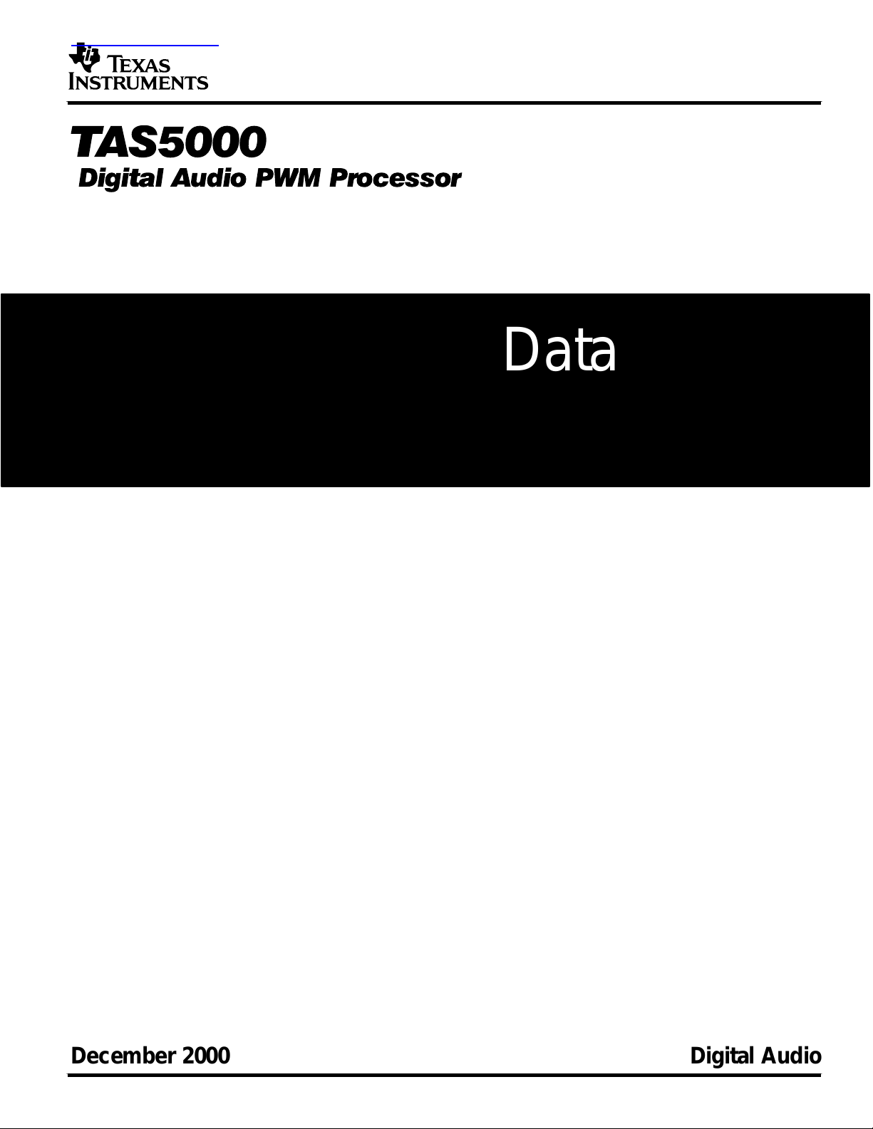
1.2 Functional Block Diagram
PLL_FLT_RET
PLL_FLT_OUT
MCLK_IN
ERR
MCLK_OUT
XTL_IN
XTL_OUT
OSC_CAP
LRCLK
SCLK
SDIN
Serial
Audio
Port
Control Section
Audio Port
Configuration
MOD0
MOD1
MOD2
DEM_SEL
PLL/Clock
Generator
Interpolation
MUTE
RESET
DEM_EN
Digital
Filter
PDN
FTEST
STEST
PTEST
DBSPD
Equibit
Modulator
M_S
DVDD1
DVSS1
DVDD2
OSC
DVSS2
DVDD3_L
Buffer
DVSS3_L
DVSS3_R
DVDD3_R
AVSS1
AVDD1
AVSS2
AVDD2
PWM_P_L
PWM_M_L
PWM_P_R
PWM_M_R
1–2
Page 7
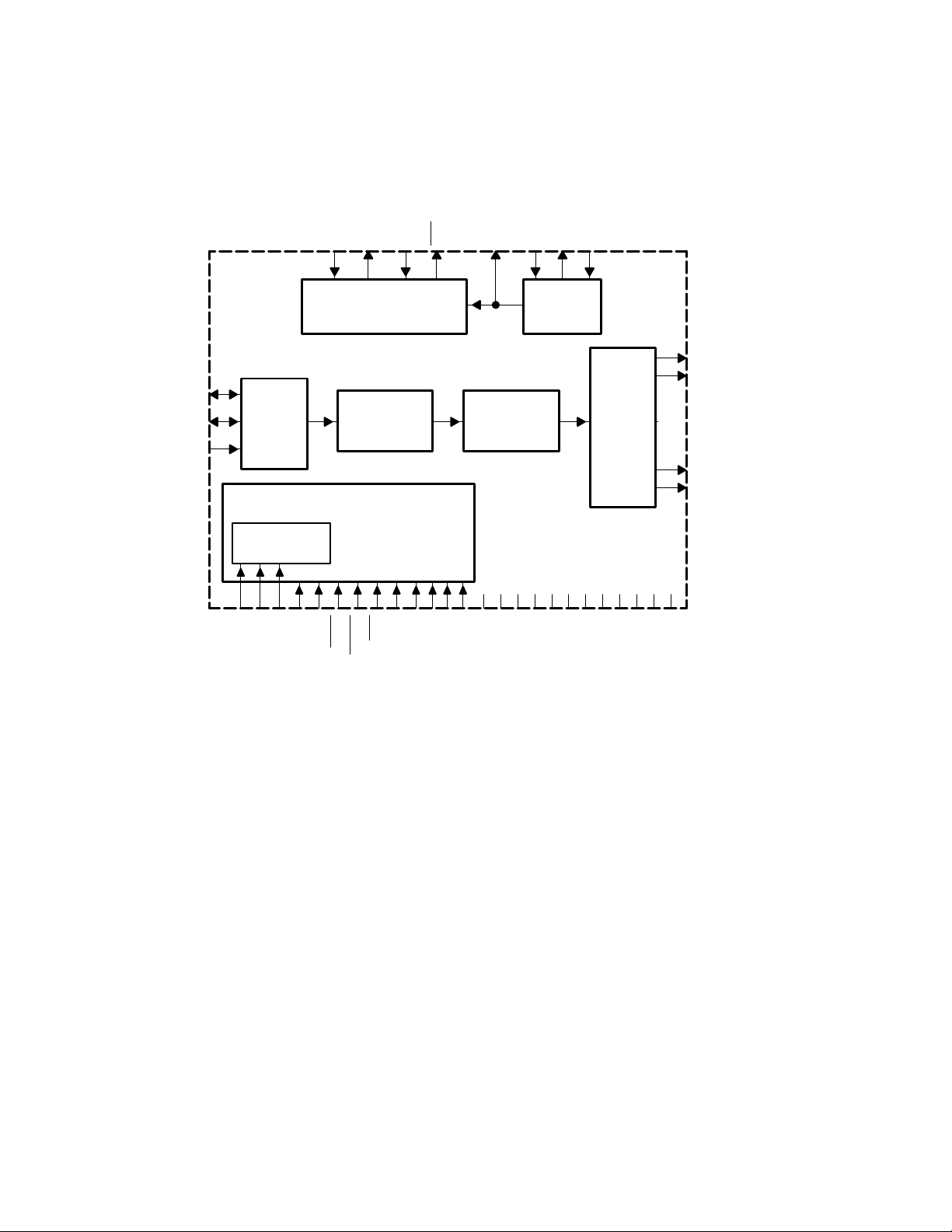
1.3 Suggested System Block Diagrams
See application notes for more details.
Digital Audio
• USB
• IEEE 1394
• SPDIF
• ADC
• Automotive
MOST
Network
IIC
Audio
Control
Figure 1–1. System #1: Stereo Configuration Using Two TAS5100 Amplifiers
TAS3001
• Digital Parametric EQ
• Volume
• DRC
• Bass
• Treble
• Serial Audio Input Port
• Internal PLL
TAS5000
Left
Right
TAS5100
TAS5100
• 2 Mono H-Bridges
TAS5100
TAS5100
• 2 Mono H-Bridges
Digital Audio
• DSP
• Volume
• EQ
• DRC
Left
TAS5000
Right
• Serial Audio Input Port
• Internal PLL
• Bass
• Treble
• Surround Processing
• AC-3 DTS Decode
Figure 1–2. System #2: Stereo Configuration With DSP
1–3
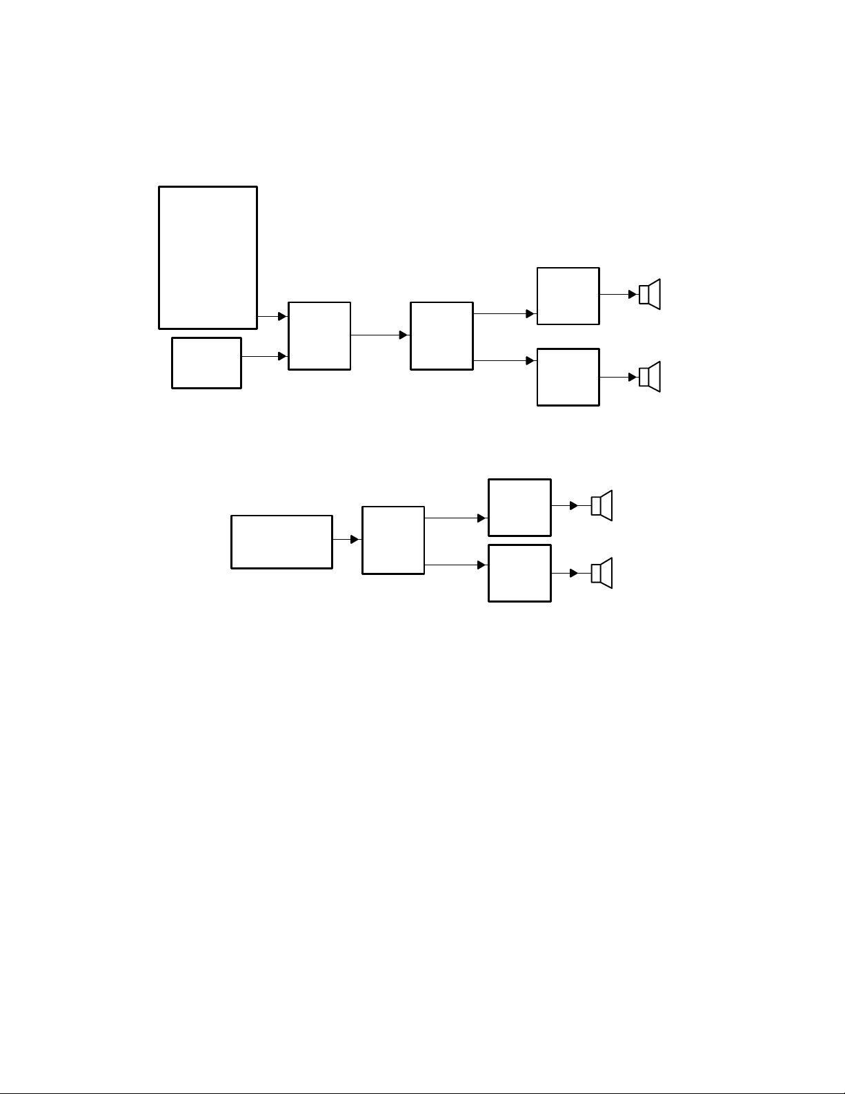
Page 8
CH1
TAS5100
Home Theater
DVD 6-Channel
Encoded Digital
Audio Source
TAS5000
6
DSP 6-Channel
Decode
• Dolby AC-3
TAS5000
CH2
CH3
CH4
TAS5100
TAS5100
• DTS
• Volume
• EQ
TAS5100
• DRC
• Bass
• Treble
TAS5100
CH5
TAS5000
CH6
TAS5100
Figure 1–3. System #3: 6-Channel Audio Playback
1–4
Page 9

1.4 Terminal Assignments
48-Pin TQFP PACKAGE
(TOP VIEW)
AVDD1
XTL_IN
XTL_OUT
OSC_CAP
AVSS1
FTEST
DEM_EN
DEM_SEL
STEST
DBSPD
MUTE
DVSS3_L
MCLK_IN
AVDD2
PLL_FLT_OUT
PLL_FLT_RET
AVSS2
RESET
PDN
PTEST
M_S
DVDD1
NC – No internal connection
1.5 Ordering Information
T
A
0°C to 70°C TAS5000PFB
NC
NC
47 46 45 44 4348 42
1
2
3
4
5
6
7
8
9
10
11
12
14 15
13
DVSS1
DVDD1
PACKAGE
17 18 19 20
16
SCLK
DVSS1
MCLK_OUT
SDIN
LRCLK
40 39 3841
22 23 24
21
MOD2
MOD1
37
ERR
MOD0
36
DVDD3_L
35
PWM_P_L
34
PWM_M_L
33
NC
32
NC
31
DVDD2
30
DVSS2
29
PWM_P_R
28
PWM_M_R
27
NC
NC
26
DVDD3_R
25
DVSS3_R
1–5
Page 10

1.6 Terminal Functions
I/O
DESCRIPTION
TERMINAL
NAME NO.
AVDD1 48 I Analog supply for oscillator
AVDD2 2 I Analog supply for PLL
AVSS1 44 I Analog ground for oscillator
AVSS2 5 I Analog ground for PLL
DBSPD 39 I Indicates sample rate is double speed (88.2 kHz or 96 kHz), active high
DEM_EN 43 I De-emphasis enable, active high
DEM_SEL 42 I De-emphasis select (0 = 44.1 kHz, 1 = 48 kHz)
DVDD1 12, 14 I Digital voltage supply for logic
DVDD2 31 I Digital voltage supply for PWM reclocking
DVDD3_L 36 I Digital voltage supply for PWM output (left)
DVDD3_R 25 I Digital voltage supply for PWM output (right)
DVSS1 13, 15 I Digital ground for Logic
DVSS2 30 I Digital ground for PWM reclocking
DVSS3_L 37 I Digital ground for PWM output (left)
DVSS3_R 24 I Digital ground for PWM output (right)
ERR 23 O System error flag, active low
FTEST 41 I Tied to DVSS1 for normal operation
LRCLK 18 I/O Left/right clock (input when M_S = 0; output when M_S = 1)
MCLK_IN 1 I MCLK input
MCLK_OUT 16 O Buffered system clock output if M_S = 1; otherwise set to 0
MOD0 22 I Serial interface selection pin, bit 0
MOD1 21 I Serial interface selection pin, bit 1
MOD2 20 I Serial interface selection pin, bit 2 (MSB)
M_S 10 I Master/slave, Master=1, Slave=0
MUTE 38 I Muted signal = 0, Normal mode = 1
NC 6, 11, 26, 27,
32, 33
OSC_CAP 45 I Oscillator cap return
PDN 8 I Power down, active low
PTEST 9 I T ied to DVSS1 for normal operation
PLL_FLT_OUT 3 O Output terminal for external PLL filter
PLL_FLT_RET 4 I Return for external PLL filter
PWM_M_L 34 O PWM left output (differential –) Positive H-bridge side
PWM_M_R 28 O PWM right output (differential –) Positive H-bridge side
PWM_P_L 35 O PWM left output (differential +) Positive H-bridge side
PWM_P_R 29 O PWM right output (differential +) Positive H-bridge side
RESET 7 I Reset (active low)
SCLK 17 I/O Shift clock (input when M_S = 0, output when M_S = 1)
SDIN 19 I Stereo serial audio data input
STEST 40 I Tied to DVSS1 for normal operation
XTL_IN 47 I Crystal or clock input (MCLK input)
XTL_OUT 46 O Crystal output (not for external usage) NC when XTL_IN is MCLK input
No connection
1–6
Page 11

2 Functional Description
2.1 Serial Audio Port
The serial audio port consists of a shift clock (SCLK pin), a left/right frame synchronization clock (LRCLK pin), and
a data input (SDIN pin). The serial audio port supports standard serial PCM formats (Fs = 44.1 kHz, 48 kHz, 88.2 kHz,
or 96 kHz) stereo. See section 2.8 for Serial Interface Formats.
2.2 System Clocks – Master Mode and Slave Mode
The T AS5000 allows multiple system clocking schemes. In this document, master mode indicates that the T AS5000
provides system clocks to other parts of the system (M_S=1). Audio system clocks of frequency 256Fs MCLK_OUT ,
64 Fs SCLK, and Fs LRCLK are output from this device when it is configured in master mode. Slave mode indicates
that a system master other than the TAS5000 provides system clocks (LRCLK, SCLK, and MCLK_IN) to the T AS5000
(M_S = 0). The TAS5000 operates with LRCLK and SCLK synchronized to MCLK. TAS5000 does not require any
specific phase relationship between LRCLK and MCLK, but there must be synchronization. If the synchronization
between MCLK and LRCLK changes more than 10 MCLK periods during one sample period (LRCLK), the T AS5000
will initiate an internal reset. In the slave mode MCLK_OUT is driven low. Table 2–1 shows all the possible master
and slave modes.
2.3 Oscillator/Sampling Frequency
The sampling frequency is determined by the crystal (master mode) or master clock in (slave mode) which should
be either 1 1.2896 MHz (Fs = 44.1 kHz) or 12.288 MHz (Fs = 48 kHz). T wice the normal sampling frequency can be
selected by using the DBSPD pin which allows usage of Fs = 88.2 kHz or Fs = 96 kHz. In the double-speed slave
mode (DBSPD = 1, M_S = 0), the external clock input is either 22.5796 MHz (Fs = 88.2 kHz) or 24.576 MHz
(Fs = 96 kHz). Table 2–1 explains the proper clock selection.
2.4 Phase Locked Loop (PLL)/Clock Generation
A low jitter PLL is incorporated for internal use. Connections for the PLL external loop filter are provided as
PLL_FL T_RET and PLL_FLT_OUT . See Figure 5–1 for a suggested external loop filter. If the PLL loses lock, the error
status pin (ERR
Reporting.
) will go low. Note that ERR can go low for other conditions as well. See section 2.7.7 Error Status
2–1
Page 12

Table 2–1. Oscillator, External Clock, and PLL Functions
DESCRIPTION M_S DBSPD
Master, normal speed 1 0 11.2896 — 2.8224 44.1 11.2896
Master, normal speed 1 0 12.288 — 3.072 48 12.288
Master, double speed 1 1 — 22.5792§5.6448 88.2 22.5792
Master, double speed 1 1 — 24.576
Slave, normal speed 0 0 — 11.2896§2.8224 44.1 Digital GND
Slave, normal speed 0 0 — 12.288
Slave, double speed 0 1 — 22.5792§5.6448 88.2 Digital GND
Slave, double speed 0 1 — 24.576
†
Either a crystal oscillator or an external clock of the specified frequency can be connected to XTL_IN.
‡
MCLK_IN tied low when input to XTL_IN is provided; XTL_IN tied low when MCLK_IN is provided.
§
External MCLK connected to MCLK_IN input
¶
SCLK and LRCLK are outputs when M_S=1, inputs when M_S=0.
#
MCLK_OUT is driven low when M_S=0.
XTL_IN
(MHz)
†
MCLK_IN
‡
(MHz)
SCLK
(MHz)
§
§
§
LRCLK
¶
6.144 96 24.576
3.072 48 Digital GND
6.144 96 Digital GND
(kHz)
¶
MCLK_OUT
(MHz)
#
2.5 Digital Interpolation Filter
The 24-bit high performance linear phase FIR interpolation filter up-samples the input digital data at a rate of 4 times
(double speed mode = 88.2 kHz or 96 kHz) or 8 times (normal mode = 44.1 kHz or 48 kHz) the incoming sample rate.
This filter provides very low pass-band ripple and optimized time domain transient response for accurate music
reproduction.
2.6 Digital PWM Modulator
The interpolation filter output is sent to the modulator. This modulator consists of a high performance 4th order digital
noise shaper and a PCM to PWM converter. Following the noise shaper , the PCM signal is fed into a very low distortion
PCM to PWM conversion block, buffered and output from the chip. The modulation scheme is based on a 2-state
control of the H-bridge output.
2.7 Control, Status, and Operational Modes
The TAS5000 control section consists of several control-input pins. Three serial mode pins (MOD0, MOD1, and
MOD2) are provided to select various serial data formats. During normal operating conditions if any of the MOD0,
MOD1, or MOD2 pins changes state, a reset sequence is initiated (see paragraph 2.7.2). Also provided are separate
power-down (PDN
2.7.1 Power Up
At power up the ERR pin is asserted low and the PWM outputs go to the hard mute state in which the P outputs are
held low and the M outputs are held high. Following initialization, the TAS5000 will come up in the operational state.
There are two cases of power-up timing. The first case is shown in Figure 2–1 with RESET
second case is shown in Figure 2–2 with PDN
), reset (RESET), and mute (MUTE) pins. The ERR pin indicates that an error has occurred.
preceding PDN. The
preceding RESET.
RESET
PDN
Initialization Time = 4224 LRCLK Periods
ERR
Figure 2–1. Power-Up Timing (RESET preceding PDN)
2–2
Page 13

Greater Than 16 MCLK Periods
RESET
PDN
Initialization Time = 256 LRCLK Periods
ERR
Figure 2–2. Power-Up Timing (PDN preceding RESET)
2.7.2 Reset
The reset signal for the TAS5000 should be applied whenever toggling the M_S, DBSPD signal. This reset is
asynchronous. See Figure 2–3 for reset timing. T o initiate the reset sequence the RESET
as the pin is held low the chip is in the reset state. During this reset time the PWM outputs are hard-muted (P-outputs
held low and M-outputs held high) and the ERR
status pin is held low. Assuming PDN is high, the rising edge of the
reset pulse begins chip initialization. After 256 LRCLK periods the TAS5000 will begin normal operation.
RESET
pin is asserted low. As long
Initialization
ERR
Normal Operation
PDN
Normal
Operation
Figure 2–3. Reset Timing
2.7.3 Power Down
When PDN is low (see Figure 2–4. Power-Down Timing) both the PLL and the oscillator are shut down. Note that
power down is an asynchronous operation. To place the device in total power-down mode, both RESET
must be held low. As long as these pins are held low, the chip is in the power-down state and the PWM outputs are
hard muted with the P outputs held low and the M outputs held high. T o place the device back into normal mode, see
section 2.7.1 for power-up timing.
NOTE: In order for the dynamic logic to be properly powered down, the clocks should not be stopped before
the PDN
pin goes low. Otherwise, the device may drain additional supply current.
ERR
Initialization
PDN and
RESET
Normal
Operation
Chip
Power-Down
Normal Operation
Figure 2–4. Power-Down Timing
and PDN
2.7.4 Mute
The TAS5000 provides a mute function that is used when the MUTE pin is asserted low. See Table 2–2 for Mute
Description. This mute is a quiet mute; that is, the mute is accomplished by outputting a zero value waveform in which
both sides of the differential PWM outputs have a 50% duty cycle.
2–3
Page 14

Table 2–2. Mute Description
MUTE PWM_P PWM_M DESCRIPTION
0 50% Duty cycle 50% Duty cycle Mute
1 DATA DATA Normal operation
2.7.5 Double Speed
Double-speed mode is used to support sampling rates of 88.2 kHz and 96 kHz. In order to put the TAS5000 in
double-speed mode with the device in normal operating conditions, the RESET
the DBSPD pin high. After RESET
pin is brought high again, a reset sequence takes place (see paragraph 2.7.2).
pin must be held low while switching
If the change is at power up, a power up sequence is originated (see paragraph 2.7.1).
2.7.6 De-Emphasis Filter
For audio sources that have been pre-emphasized, a precision 50 µs/15 µs de-emphasis filter is provided to support
the sampling rates of 44.1 kHz and 48 kHz. Pins DEM_SEL and DEM_EN select the de-emphasis functions. See
Figure 2–5 for a graph showing the de-emphasis filtering characteristics. See Table 2–3 for de-emphasis selection.
When the DEM_EN pin or the DEM_SEL pin change state, the PWM outputs go into the quiet mute state. After 128
LRCLK periods for initialization, the PWM outputs are driven to the normal (unmuted) mode.
0
De–emphasis
–10
Response – dB
3.18 (50 µs) 10.6 (15 µs)
f – Frequency – kHz
Figure 2–5. De-Emphasis Filter Characteristics
2.7.6.1 De-Emphasis Selection
De-emphasis selection is accomplished by using the DEM_SEL and DEM_EN pins. See T able 2–3 for de-emphasis
selection description.
Table 2–3. De-Emphasis Selection
DEM_SEL DEM_EN DESCRIPTION
X 0 De-emphasis disabled
0 1 De-emphasis enabled for Fs = 44.1 kHz
1 1 De-emphasis enabled for Fs = 48 kHz
2.7.7 Error Status Reporting (ERR pin)
The following is a list of the error conditions that will cause the ERR status pin to be asserted low:
• No clocks
• Clock phase errors
When any of the above conditions is met, the ERR
If the error condition is removed, the TAS5000 is reinitialized and the ERR
will go low and the PWM outputs will go to the hard mute state.
pin will be asserted high.
2.8 Serial Interface Formats
The T AS5000 is compatible with eight different serial interfaces. Available interface options are IIS, right justified, left
justified, and DSP Frame. Table 2–4 indicates how these options are selected using the MOD0, MOD1, and MOD2
pins.
2–4
Page 15

Table 2–4. Hardware Selection of Serial Audio Modes
MODE MOD2 PIN MOD1 PIN MOD0 PIN
0 0 0 0 16 bit, MSB first; right justified
1 0 0 1 20 bit, MSB first; right justified
2 0 1 0 24 bit, MSB first; right justified
3 0 1 1 16 bit IIS
4 1 0 0 20 bit IIS
5 1 0 1 24 bit IIS
6 1 1 0 16 bit MSB first, left justified
7 1 1 1 16 bit DSP frame
SERIAL INTERFACE
SDIN
The following figures illustrate the relationship between the SCLK, LRCLK and the serial data I/O for the different
interface protocols. Note that there are always 64 SCLKs per LRCLK. The nondata bits are padded with binary 0.
2.8.1 MSB First Right Justified (for 16-, 20-, 24-bits)
SCLK
LRCLK = Fs
SDIN
X MSB LSB X MSB LSB
Left Channel Right Channel
Figure 2–6. MSB First Right Justified
Note the following characteristics of this protocol.
• Left channel is received when LRCLK is high.
• Right channel is received when LRCLK is low.
• The SDIN data is justified to the trailing edge of the LRCLK
• SDIN is sampled at the rising edge of SCLK.
• If LRCLK phase changes by more than 10 MCLKs, then the chip automatically resets.
2.8.2 IIS Compatible Serial Format ( for 16-, 20-, 24-bits)
SCLK
LRCLK = Fs
SDIN
X MSB LSB X MSB LSB
Left Channel Right Channel
Figure 2–7. IIS Compatible Serial Format
Note the following characteristics of this protocol.
2–5
Page 16
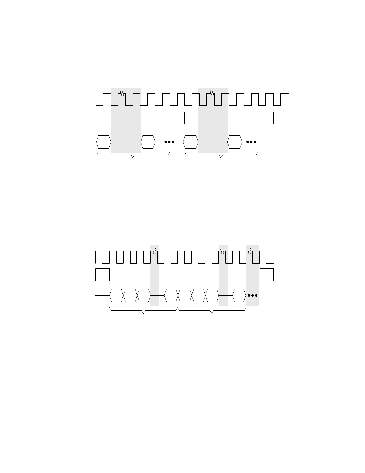
• Left channel is received when LRCLK is low.
• Right channel is received when LRCLK is high.
• SDIN is sampled with the rising edge of SCLK.
2.8.3 MSB Left Justified Serial Interface Format (for 16 bits)
SCLK
LRCLK = Fs
SDIN
MSB LSB MSB LSB
Left Channel Right Channel
Figure 2–8. MSB Left Justified Serial Interface Format
Note the following characteristics of this protocol.
• Left channel is received when LRCLK is high.
• Right channel is received when LRCLK is low.
• The SDIN data is justified to the leading edge of the LRCLK.
• SDIN is sampled with the rising edge of SCLK.
2.8.4 DSP Compatible Serial Interface Format (for 16 bits)
SCLK
LRCLK = Fs
SDIN
15 14 13 0 15 14 13 0
Left Channel
(MSB = 15)
Figure 2–9. DSP Compatible Serial Interface Format
Note the following characteristics of this protocol.
• Serial data is sampled with the falling edge of SCLK.
2.9 PWM Outputs
Designed to be used with TAS5100.
2–6
Right Channel
(MSB = 15)
Page 17

3 Electrical Specifications
Supply current
Digital
Power dissipation
Digital
Supply current
Analog
Power dissipation
Analog
3.1 Absolute Maximum Ratings
Analog supply voltage range, AV
Digital power supply voltage, DV
Digital input voltage, V
Operating free-air temperature, T
Storage temperature, T
(see Note 1) –0.3 V to DV
I
–65°C to 150°C. . . . . . . . . . . . . . . . . . . . . . . . . . . . . . . . . . . . . . . . . . . . . . . . . . . . . . . .
stg
†
AV
DD1,
DV
DD1,
0°C to 70°C. . . . . . . . . . . . . . . . . . . . . . . . . . . . . . . . . . . . . . . . . . . . . . . . . . . .
A
) –0.3 V to 4.2 V. . . . . . . . . . . . . . . . . . . . . . . . . . . . . . . . . . . . . . .
DD2
DD2,
DV
DD3_L,
DV
–0.3 V to 4.2 V. . . . . . . . . . . . . . . . . . . . .
DD3_R
DDX
+0.3 V. . . . . . . . . . . . . . . . . . . . . . . . . . . . . . . . . . . . . . . .
ESD 2000 V. . . . . . . . . . . . . . . . . . . . . . . . . . . . . . . . . . . . . . . . . . . . . . . . . . . . . . . . . . . . . . . . . . . . . . . . . . . . . . . . . . .
†
Stresses beyond those listed under “absolute maximum ratings” may cause permanent damage to the device. These are stress ratings only and
functional operation of the device at these or any other conditions beyond those indicated under “recommended operating conditions” is not
implied. Exposure to absolute-maximum-rated conditions for extended periods may affect device reliability.
NOTES: 1. DVDD1, DVDD2, DVDD3_L, DVDD3_R
3.2 Recommended Operating Conditions
(TA = 25°C; DV
Voltages at analog inputs and outputs are with respect to ground
Supply voltage Digital DVDDX
pp
p
Supply voltage Analog AVDDX
pp
p
‡
DVDD1, DVDD2, DVDD3_L, DVDD3_R
§
If the clocks are turned off
¶
AVDD1, AVDD2
DD1
= DV
DD2
= DV
DD3_L
= DV
= 3.3 V ±10%, A V
DD3_R
= A V
DD1
‡
Operating 18 mA
Power down
Operating 59.4 mW
Power down
¶
Operating 8 mA
Power down
Operating 26.4 mW
Power down
= 3.3 V ±10%, Fs = 44.1 kHz)
DD2
MIN TYP MAX UNIT
3 3.3 3.6 V
§
§
§
§
2 20 µA
6.6 72 µW
3 3.3 3.6 V
10 100 µA
33 360 µW
3–1
Page 18

3.3 Electrical Characteristics
3.3.1 Static Digital Specifications
(TA = 25°C; DV
V
V
V
V
High-level input voltage 2 DVDD1 V
IH
Low-level input voltage 0 0.8 V
IL
High-level output voltage, (IO = –1 mA) 2.4 V
OH
Low-level output voltage, (IO = 4 mA) 0.4 V
OL
Input leakage current –10 10 µA
DD1
= DV
DD2
= DV
DD3_L
= DV
DD3_R
= 3.3 V ±10%, A V
DD1
= AV
= 3.3 V ±10%)
DD2
MIN MAX UNIT
3.3.2 Digital Interpolation Filter and PWM Modulator
(TA = 25°C; DV
All the terms characterized by frequency will scale with the normal mode sampling frequency, Fs.
Pass band 0 20 kHz
Pass band ripple ±0.012 dB
Stop band 24.1 kHz
Stop band attenuation (24.1 kHz to 152.3 kHz) 50 dB
Group delay 700 µS
PWM modulation index (gain) 0.93
DD1
= DV
DD2
= DV
DD3_L
= DV
= 3.3 V ±10%, A V
DD3_R
DD1
= A V
= 3.3 V ±10%, Fs = 44.1 kHz)
DD2
MIN TYP MAX UNIT
3.3.3 TAS5000/TAS5100 System Performance Measured at the Speaker Terminals
Reference section 4.4 in the TAS5100 Data Manual
3.4 Switching Characteristics
3.4.1 Serial Audio Ports Slave Mode
(T
= 25°C, DV
A
f(SCLK) SCLK frequency 6.144 MHz
tsu(SDIN) SDIN setup time before SCLK rising edge 20 ns
th(SDIN) SDIN hold time from SCLK rising edge 10 ns
F(LRCLK) LRCLK frequency 44.1 48 96 kHz
tsu(LRCLK) LRCLK edge setup before SCLK rising edge 20 ns
= DV
DD1
MCLK duty cycle 50%
SCLK duty cycle 50%
LRCLK duty cycle 50%
DD2
= DV
= DV
DD3_L
PARAMETER MIN TYP MAX UNIT
DD3_R
= AV
DD1
= AV
= 3.3 V ±10%)
DD2
3–2
Page 19

3.4.2 Serial Audio Ports Master Mode
Load conditions: 50pF
= 25°C, DV
(T
A
t
(MSD)
t
(MLRD)
MCLK to SCLK 0 5 ns
MLCK to LRCLK 0 5 ns
SCLK, LRCLK duty cycle 50%
DD1
= DV
DD2
= DV
= DV
DD3_L
PARAMETER MIN TYP MAX UNIT
DD3_R
= AV
DD1
= AV
= 3.3 V ±10%)
DD2
3.4.3 DSP Serial Interface Mode
(T
= 25°C, DV
A
f(SCLK) SCLK frequency 6.144 MHz
tW(FSHIGH) Pulse duration, sync 1/(64×fs) ns
tsu(SDIN),
tsu(LRCLK)
th(SDIN),
th(LRCLK)
= DV
DD1
SDIN and LRCLK setup time before SCLK falling edge 20 ns
SDIN and LRCLK hold time from SCLK falling edge 10 ns
SCLK duty cycle 50%
DD2
= DV
= DV
DD3_L
PARAMETER MIN TYP MAX UNIT
DD3_R
= AV
DD1
= AV
= 3.3 V ±10%)
DD2
3–3
Page 20

3–4
Page 21

4 Parameter Measurement Information
SCLK
t
h(SDIN)
SDIN
t
su(SDIN)
Figure 4–1. Right Justified, IIS, Left Justified Serial Protocol Timing
SCLK
t
su(LRCLK)
LRCLK
NOTE: Serial data is sampled with the rising edge of SCLK (setup time = 20 ns and hold time = 10 ns)
Figure 4–2. Right, Left, and IIS Serial Mode Timing Requirement
SCLK
LRCLK
(Output)
t
(MSD)
t
(MLRD)
MCLK
(Output)
SCLK
LRCLK
SDIN
Figure 4–3. Serial Audio Ports Master Mode Timing
t
su(LRCLK)
t
w(FSHIGH)
t
su(SDIN)
t
h(LRCLK)
Figure 4–4. DSP Serial Port Timing
t
h(SDIN)
4–1
Page 22

SCLK
LRCLK
t
w(FSHIGH)
64 fs
SDIN
16-Bit Left Channel Data 16-Bit Left Channel Data 16-Bit Left Channel Data32-Bit Ignore
Figure 4–5. DSP Serial Port Expanded Timing
SCLK
t
su(SDIN)
SDIN
NOTE: Serial data is sampled with the falling edge of SCLK (setup time = 20 ns and hold time = 10 ns)
= 20 ns
t
h(SDIN)
= 10 ns
Figure 4–6. DSP Absolute Timing Requirement
4–2
Page 23

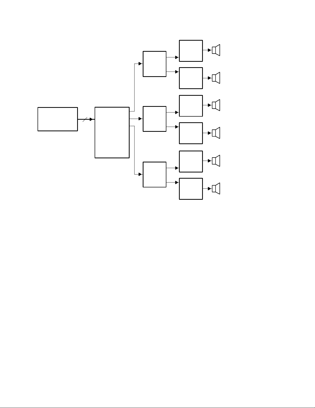
5 Application Information
†
C
1
3.3 V DIG
†
C
2
R
Audio
Source
Clock
Generator
PLL_FLT_RET
†
1
PLL_FLT_OUT
DEM_SEL
DEM_EN
DBSPD
SDIN
LRCLK
SCLK
MCLK_IN
MOD0
MOD1
MOD2
M_S
XTL_IN
PWM_P_L
PWM_M_L
ERR
RESET
PWM_P_R
PWM_M_R
MUTE
PDN
TAS5100
H-Bridge
TAS5100
H-Bridge
Micro-
Controller
†
See application note for values
Figure 5–1. Connection Diagram, Slave Mode (typical)
5–1
Page 24

5–2
 Loading...