

Page 1
ADVANCE INFORMATION
User's Guide
SLAU757–January 2018
TAS3251 Evaluation Module
This user's guide describes the characteristics, operation, and use of the TAS3251 evaluation module. A
complete printed-circuit board (PCB) description, schematic diagram, and bill of materials (BOM) are also
included. For questions and support go to the E2E forums (e2e.ti.com).
The main contents of this document are:
• Hardware descriptions and implementation
• Design information
Related documents:
• TPA3245 115-W Stereo, 230-W Mono PurePath™ Ultra-HD Analog-Input Class-D Amplifier data sheet
SLAU757–January 2018
Submit Documentation Feedback
Copyright © 2018, Texas Instruments Incorporated
TAS3251 Evaluation Module
1
Page 2

TAS32xx
PWM A
PWM B
PWM C
PWM D
I2S Input
MCLK
BCLK
LRCLK
Data
Copyright © 2017, Texas Instruments Incorporated
ADVANCE INFORMATION
Quick Start (BTL Mode)
1 Quick Start (BTL Mode)..................................................................................................... 2
2 Schematic and Bill of Materials ............................................................................................ 6
1 Output Configuration BTL .................................................................................................. 2
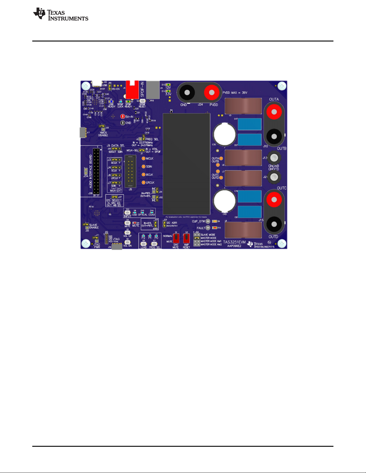
2 EVM Board (Top Side)...................................................................................................... 3
3 EVM Board (Bottom Side) .................................................................................................. 4
4 TAS3251EVM Schematics (1 of 6)........................................................................................ 6
5 TAS3251EVM Schematics (2 of 6)........................................................................................ 7
6 TAS3251EVM Schematics (3 of 6)........................................................................................ 8
7 TAS3251EVM Schematics (4 of 6)........................................................................................ 9
8 TAS3251EVM Schematics (5 of 6) ...................................................................................... 10
9 TAS3251EVM Schematics (6 of 6) ...................................................................................... 11
1 Jumper and Switch Configurations (USB BTL Mode) .................................................................. 4
2 TAS3251EVM Bill of Materials ........................................................................................... 12
Trademarks
PurePath is a trademark of Texas Instruments.
All other trademarks are the property of their respective owners.
www.ti.com
Contents
List of Figures
List of Tables
1 Quick Start (BTL Mode)
Figure 1 shows the output configuration BTL.
1.1 Required Hardware
The following is required for this EVM configuration:
• TAS3251EVM
• Power supply 5–17 A, 15–36 V
• Two cables for for power supply connection
• Two 3–8 Ω speakers or resistor loads (ensure speaker or load is appropriately sized for required
wattage output)
• Four cables for banana or terminal to speaker or load connection
• USB micro cable
• PC with PurePath™ Console 3 (PPC3) and audio track
Figure 1. Output Configuration BTL
2
TAS3251 Evaluation Module
Copyright © 2018, Texas Instruments Incorporated
SLAU757–January 2018
Submit Documentation Feedback
Page 3
ADVANCE INFORMATION
www.ti.com
1.2 Connections and Board Configuration (USB BTL Mode)
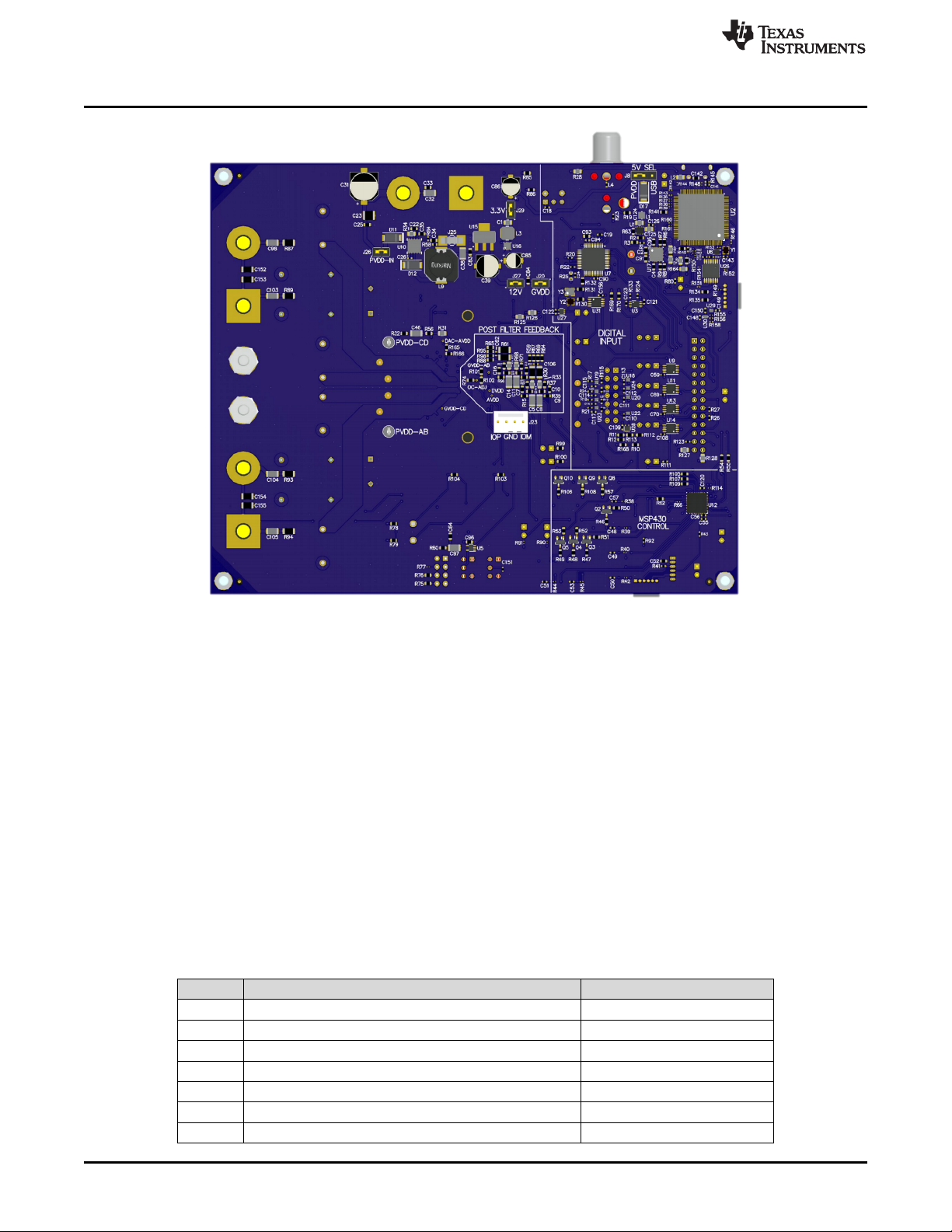
Figure 2 and Figure 3 illustrate the top and bottom EVM boards.
Quick Start (BTL Mode)
Figure 2. EVM Board (Top Side)
SLAU757–January 2018
Submit Documentation Feedback
Copyright © 2018, Texas Instruments Incorporated
TAS3251 Evaluation Module
3
Page 4
ADVANCE INFORMATION
Quick Start (BTL Mode)
www.ti.com
Figure 3. EVM Board (Bottom Side)
Use the following when connecting and configuring the board for 48-kHz USB BTL mode:
1. Ensure the power supply is OFF. Connect the power supply positive terminal to J24 PVDD (red) and
negative to J1 GND (black).
2. Connect the left channel speaker or power resistor load (3–8 Ω) to the TAS3251EVM OUTA terminal
(J10 OUTA (red)) and the other side of the speaker or resistor load to the TPA3251EVM OUTB
terminal (J10 OUTB (black)).
3. Connect the right channel speaker or power resistor load (3–8 Ω) to the TAS3251EVM OUTA terminal
(J15 OUTA (red)) and the other side of the speaker or resistor load to the TPA3251EVM OUTB
terminal (J15 OUTB (black)).
4. Check to make sure that the power supply is connected to J24 only, and the speakers or resistor loads
are connected to J10 or J15 only, as their colors are the same.
5. Connect USB cable from the PC to the TAS3251EVM.
6. Ensure that DAC MUTE S1 and AMP RESET S3 are in the lower positions of MUTE and RESET.
7. Check Table 1 for all jumper and switch configurations.
Table 1. Jumper and Switch Configurations (USB BTL Mode)
Jumper Description Configuration for BTL
J16 HS-EN USB high-speed enable Do not care
J33 XMOS DISABLE Remove
J2 Frequency select Remove
J30 Data select for J9 Do not care
J1 MCLK-SEL Install
J3 MCLK 1-2
J4 SCLK 1-2
4
TAS3251 Evaluation Module
Copyright © 2018, Texas Instruments Incorporated
SLAU757–January 2018
Submit Documentation Feedback
Page 5
ADVANCE INFORMATION
www.ti.com
Quick Start (BTL Mode)
Table 1. Jumper and Switch Configurations (USB BTL Mode) (continued)
Jumper Description Configuration for BTL
J5 LRCLK 1-2
J7 SDIN 1-2
J37 I2S source select Install
J31 PBTL INC Remove
J32 PBTL IND Remove
J14 MODE Install
J19 ADR Install
J22 PWM switching frequency 3-4
J35 SLAVE ENABLE Remove
J11 JTAG power Do not care
J26 PVDD Install
J29 3.3V Install
J27 12V Install
J20 GVDD Install
J8 5-V select 1-2
S1 DAC MUTE MUTE
S3 AMP RESET RESET
1.3 Power Up
Ensure that the required connections and configurations have been checked. The TAS3251EVM board
can now be powered on.
1. Enable the power supply at 15 V to 36 V and ensure that D13 and D14 illuminates. LEDs D9 and D10
should not be illuminated.
2. Bring the DAC out of MUTE by switching DAC MUTE (S1) to NORMAL.
3. Bring the Power Stage out of RESET by switching AMP RESET (S3) to the high position. You should
see the FAULT LED (D10) blink once quickly, then remain unilluminated.
SLAU757–January 2018
Submit Documentation Feedback
Copyright © 2018, Texas Instruments Incorporated
TAS3251 Evaluation Module
5
Page 6
GND
47.0k
R157
3.3V
1A
1
GND
2
2A32Y
4
VCC
5
1Y
6
U29
SN74LVC2G07DSFR
3.3V
VDDIOL
6
VDD
11
VDDIOL
14
VDD
16
VDD
17
VDDIOL
19
VDD
24
VDDIOL
29
VDD
36
VDD
41
VDDIOL
42
VDDIOR
52
VDD
56
VDD
60
NC
65
VDDIOR
67
VDD
73
VDDIOR
78
VDD
80
VDD
81
VDDIOR
83
VDD
87
VDDIOR
92
VDD
101
VDD
102
PLL_AVDD
103
PLL_AGND
104
OTP_VCC
105
VDDIOT
110
VDDIOT
111
VDD
120
USB_VDD33
44
USB_VDD
49
NC
50
VDD
126
PAD
129
XEF216-512-TQ128-C20
U2E
3.3V 1.0V
3.3V
1.0V
GND
4.75
R140
0.1µF
C82
GND
X0D36
3
X0D37
4
X0D38
5
X0D39
7
X0D40
8
X0D41
9
X0D42
10
X0D43
12
X0D01
27
X0D10
28
X0D00
30
X0D04
31
X0D11
32
X0D05
33
X0D06
34
X0D07
35
X0D02
37
X0D03
38
X0D08
39
X0D09
40
X0D14
57
X0D15
58
X0D20
59
X0D21
61
X0D12
62
X0D13
63
X0D22
64
X0D23
66
X0D16
68
X0D17
69
X0D18
70
X0D19
71
X0D24
88
X0D25
89
X0D34
90
X0D35
91
X0D26
93
X0D27
94
X0D32
95
X0D28
96
X0D33
97
X0D29
98
X0D30
99
X0D31
100
XEF216-512-TQ128-C20
U2A
1.00k
R110
3.3V
GND
3.3V
GND
3.3V
10.0k
R144
3.3V
GND
X-HS-EN
L2
USB_D_P
USB_D_M
USB_ID
GND
X1D35
13
X1D36
15
X1D37
18
X1D38
20
X1D18
25
X1D19
26
X1D14
51
X1D15
53
X1D20
54
X1D21
55
X1D02
72
X1D03
74
X1D04
75
X1D05
76
X1D06
77
X1D07
79
X1D08
82
X1D09
84
X1D00
85
X1D01
86
X1D41
107
X1D42
108
X1D43
109
X1D40
106
X1D26
112
X1D27
113
X1D28
114
X1D29
115
X1D30
116
X1D31
117
X1D32
118
X1D33
119
X1D39
21
X1D16
22
X1D17
23
X1D10
121
X1D11
122
U2B
XEF216-512-TQ128-C20
EN1PG
2
FB
3
VOS
4
GND
5
SW
6
VIN
7
U1
TPS62085RLTR
22µF
C125
470nH
L1
40.2k
R1
162k
R3
1.00M
R2
5V to 1V BUCK
0.1µF
C126
22µF
C124
1.0V
GND
GND
GND
GND GND
XIN/CLK
1
S0
2
VDD
3
VCTRL
4
GND
5
VDDOUT
6
VDDOUT
7
Y3
8
Y2
9
GND
10
Y1
11
SCL/S2
12
SDA/S1
13
XOUT
14
U26
CDCE913PWR
GND
3.3V
VCCA
1
A1
2
A2
3
GND
5
B2
6
B1
7
OE
4
VCCB
8
U6
SN74AVC2T244DQMR
GND GND
3.3V 1.8V
ENABLE
1
GND
2
SENSE
3
SENSE_OUT
4
CT
5
VCC
6
U30
TPS3897ADRYR
3.3V
25.5k
R156
1.0V
51.0k
R158
10.0k
R155
3.3V
470pF
C150
GND
GND
GND
10.0k
R149
10.0k
R150
X-24M
X-MCLK
3.3V
Blue
D1
USB RDY
560
R141
2.2µF
C142
GND
GND GND
X-MCLK
47.0k
R136
3.3V 3.3V
3.3V
USB I/O
USB_ID
43
USB_VBUS
45
USB_DP
46
USB_DM
47
USB_RTUNE
48
XEF216-512-TQ128-C20
U2C
43.2
R148
0.1µF
C141
GND
GND
10.0k
R145
X-TCK
X-TMS
X-TDO
X-TDI
X-TRSTN
X-RSTN
TRST
123
RST
124
CLK
125
TMS
127
TCK
128
TDO
1
TDI
2
XEF216-512-TQ128-C20
U2D
X-24M
X-TCK
X-TMS
X-TDO
X-TDI
X-RSTN
TRST
XMOS AND I/Os
0
R147
VDD
4
OE/STANDBY1GND
2
OUT
3
24
MHz
Y1
3.3V
GND
10.0k
R154
JTAG
CLOCK GENERATION
33.2
R153
33.2R146
33.2
R151
33.2
R152
GND
0.1µF
16V
C148
3.3V
GND
0.1µF
16V
C149
3.3V
GND
3.3V
GND
3.3V
GND
3.3V
X-SCL
X-SDA
33.2R143
33.2
R142
1
2
3
4
5
6
J17
JTAG
GND
X-TDI
X-TMS
X-TCK
X-TDO
X-TRSTN
VBUS-XMOS
X-SCL
X-SDA
BCLK-USB
LRCLK-USB
SDOUT-USB
3.3V
BCLK-USB
5V
4.99k
R124
4.99k
R133
3.3V 3.3V
SDOUT-USB
BCLK-USB
LRCLK-USB
I2S
USB-SPDIF
0R134
0
R135
X-MCLK
X-SCL
X-SDA
GND
I2C
SDA
SCL
GND
3.3V
SDA_B
1
GND
2
VCCA
3
SDA_A
4
SCL_A
5
OE
6
VCCB
7
SCL_B
8
U3
TCA9406DCUR
I2C-BUF-EN
I2C BUF CTRL
I2C-BUF-EN
0.1µF
16V
C17
0.1µF
16V
C27
0.1µF
16V
C37
0.1µF
16V
C40
0.1µF
16V
C45
0.1µF
16V
C54
0.1µF
16V
C58
0.1µF
16V
C74
0.1µF
16V
C80
0.1µF
16V
C99
0.1µF
16V
C100
0.1µF
16V
C101
0.1µF
16V
C102
5V-USB
5V-USB
5V-USB
5V-USB
0.1µF
16V
C143
0.1µF
16V
C144
0.1µF
16V
C145
0.1µF
16V
C146
0.1µF
16V
C147
1.8V
1.8V 1.8V
VBUS
1
D-
2
D+
3
ID
4
GND
5
678
9
J18
USB
J16
HS-EN
GND
XMOS-ENABLE
XMOS-ENABLE
0
R159
3.3V
RESET-AMP
DAC_MUTE
FAULT
CLIP_OTW
0R160
0R161
0R162
0R163
47.0k
R137
47.0k
R138
47.0k
R139
XIN-CLK
0
R63
0
R164
3.3V
0
R167
1.0V
GND
0.1µF
16V
C127
0.1µF
16V
C128
0.1µF
16V
C129
0.1µF
16V
C130
0.1µF
16V
C131
0.1µF
16V
C132
0.1µF
16V
C133
0.1µF
16V
C134
0.1µF
16V
C135
0.1µF
16V
C136
0.1µF
16V
C137
0.1µF
16V
C138
0.1µF
16V
C139
0.1µF
16V
C140
GND
-USB
J33
10.0k
R80
ADVANCE INFORMATION
Schematic and Bill of Materials
www.ti.com
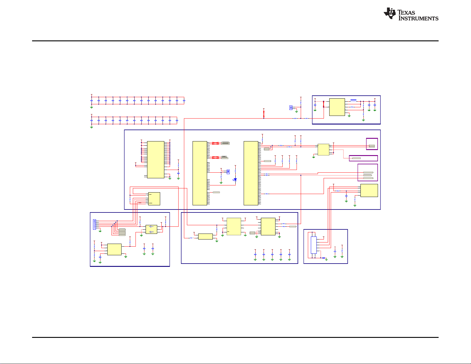
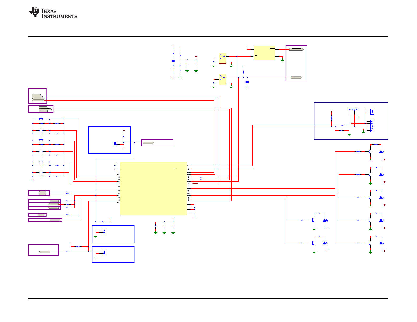
2 Schematic and Bill of Materials
This section includes the TAS3251EVM schematics and the TAS3251EVM BOM.
2.1 Schematic
Figure 4 to Figure 9 display the EVM schematics.
6
TAS3251 Evaluation Module
Figure 4. TAS3251EVM Schematics (1 of 6)
Copyright © 2018, Texas Instruments Incorporated
SLAU757–January 2018
Submit Documentation Feedback
Page 7
Q4
2.00k
R52
ADR
DUT
0R62
CLIP_OTW
FAULT
DUT
MODE
Blue
D8
USB
Q8
2.00k
R105
Blue
D15
OPTICAL
Q9
GND
2.00k
R107
Q10
GND
2.00k
R109
MUTE-LED
P2-LED
P1-LED
P0-LED
I2S MUX CONTROL
MUX_CTRL
MUX-CTRL_MCU
0
R111
ADR-MCU
GND
S4 MUTE
S5 VOL UP
S6 VOL DN
S7 PROGRAM SEL
S8 LOAD
S10 INPUT
470pF
C53
470pF
C51
470pF
C50
470pF
C49
470pF
C48
470pF
C57
25.5k
R38
25.5k
R39
25.5k
R40
25.5k
R42
25.5k
R44
25.5k
R45
AVCC
14
AVSS
13
DVCC
38
DVCC
39
DVSS
1
DVSS
4
P1.0/TA0CLK/ADC10CLK
29
P1.1/TA0.0
30
P1.2/TA0.1
31
P1.3/TA0.2
32
P1.4/SMCLK/TCK
33
P1.5/TA0.0/TMS
34
P1.6/TA0.1/TDI
35
P1.7/TA0.2/TDO/TDI
36
P2.0/TA1CLK/ACLK/A0
6
P2.1/TA0INCLK/SMCLK/A1
7
P2.2/TA0.0/A2
8
P2.3/TA0.1/A3/VREF-/VEREF-
27
P2.4/TA0.2/A4/VREF+/VEREF+
28
P2.5/TA1.0/ROSC
40
P3.0/UCB0STE/UCA0CLK/A5
9
P3.1/UCB0SIMO/UCB0SDA
10
P3.2/UCB0SOMI/UCB0SCL
11
P3.3/UCB0CLK/UCA0STE
12
P3.4/UCA0TXD/UCA0SIMO
23
P3.5/UCA0RXD/UCA0SOMI
24
P3.6/TA1.1/A6
25
P3.7/TA1.2/A7
26
P4.0/TB0.0/CA0
15
P4.1/TB0.1/CA1
16
P4.2/TB0.2/CA2
17
P4.3/TB0.0/A12/CA3
18
P4.4/TB0.1/A13/CA4
19
P4.5/TB0.2/A14/CA5
20
P4.6/TB0OUTH/A15/CA6
21
P4.7/TB0CLK/CA7
22
PAD
41
RST/NMI/SBWTDIO
5
TEST/SBWTCK
37
XIN/P2.6
3
XOUT/P2.7
2
U12
MSP430G2955IRHA40R
SBWTDIO
SBWTCK
GND
3.3V
GND
0.1µF
C56
GND
1µF
C55
0.1µF
C109
GND
I2C
SDA
0
R55 SDA-MCU
SCL
0
R54 SCL-MCU
MODE
0
R103
0
R104
SW-LOAD
SW-PROGSEL
SW-VOLDN
SW-VOLUP
SW-MUTE
SW-INPUT
SW-MUTE
SW-VOLUP
SW-LOAD
SW-PROGSEL
SW-VOLDN
3.3V
Blue
D16
COAX
3.3V
3.3V
GND
3.3V
USB-LED
OPTICAL-LED
COAX-LED
USB-LED
OPTICAL-LED
COAX-LED
GND
3.3V
GND
3.3V
Blue
D6
P1
Blue
D5
P2
560
R47
Q3
2.00k
R51
Red
D4
MUTE
Q2
2.00k
R50
Blue
D7
P0
Q5
2.00k
R53
GND
3.3V
GND
3.3V
I2S BUFFERS
SLAVE-EN
I2S-BUF-EN
J35
SLAVE ENABLE
0
R113
GND
10.0k
R114
3.3V
CLIP_OTW
FAULT
J2
FREQ SEL
GND
FREQ SELECT
FREQ-SEL
OUT = 24.576MHz
IN = 22.5792MHz
FREQUENCY
SELECT
SLAVE
ENABLE
OUT = NORMAL MODE
IN = SLAVE MODE
12345
6
J36 JTAG-RA
GND
J37
I2S SELECT
GND
I2S SELECT
OUT = AIB I2S
IN = SRC I2S
10.0k
R5
3.3V
FREQ-SEL
3.3V
AIB
3.30k
R60
GND
PVDD
100k
R32
GND
8.06k
R56
1µF
100V
C46
1µF
100V
C97
0.1uF
C64
GND
0.1uF
C96
GND
VDD-RST
GND
RESET-AMP
GND
1
GND
2
MR
5
RESET
3
VDD
4
U5
TPS3802K33DCKR
VDD-RST
GND
6
4
5
13
S3
AMP RESET
GND
GND
6
4
5
13
S1
DAC MUTE
GND
RST-AIB
P2-LED
P1-LED
P0-LED
MUTE-LED
GND
3.3V
49.9R43
47.0k
R41
3.3V
SPI BI-WIRE JTAG
VCC TOOL
TDIO
TCK
GND
J11
JTAG POWER
SBWTDIO
TCK
1
2
3
4
5
6
J12
JTAG
2200pF
C52
GND
SBWTCK
SBWTDIO
GPIO_AIB-1
GPIO_AIB-2
SW-INPUT
MUTE-AIB
DAC_MUTE
10.0k
R92
3.3V
DAC_MUTE
RST-AIB
MUTE-AIB
GPIO_AIB-1
GPIO_AIB-2
RST-AMP
TO DUT
560
R46
560
R48
560
R49
560
R106
560
R108
560
R57
0.1µF
C151
GND
GVDD
10.0k
R129
3.3V
A0-SRC
I2C BUFFERS
I2C-BUF-EN
0
R112
0R10
SRC4392
MCLK-SEL
MCLK SELECT
MCLK-SEL
ADVANCE INFORMATION
www.ti.com
SLAU757–January 2018
Submit Documentation Feedback
Figure 5. TAS3251EVM Schematics (2 of 6)
Copyright © 2018, Texas Instruments Incorporated
Schematic and Bill of Materials
TAS3251 Evaluation Module
7
Page 8

RX1+
1
RX1-
2
RX2+
3
RX2-
4
RX3+
5
RX3-
6
RX4+
7
RX4-
8
LOCK
11
RXCKO
12
TX-
31
TX+
32
AESOUT
34
BLS
35
SYNC
36
BCKA
37
LRCKA
38
SDINA
39
SDOUTA
40
SDOUTB
45
SDINB
46
LRCKB
47
BCKB
48
MCLK
25
RXCKI
13
MUTE
14
RDY
15
NC
41
CPM
18
CS/A0
19
CCLK/SCL
20
CDIN/A1
21
CDOUT/SDA
22
INT
23
RST
24
GPO1
26
GPO2
27
GPO3
28
GPO4
29
U7A
SRC4392IPFBR
GND
3.3V
GND
0.1µF
C18
33.0
R16
0.1µF
C19
0.1µF
C20
0.1µF
C21
L4
GND
RX1+
RX1-
RX2+
RX2-
3.3V
COAX SPDIF IN
OPTICAL
I2C_ADD=0xE0
4
3
1
J5
SPDIF-IN
SDOUT-USB
BCLK-USB
LRCLK-USB
0.1µF
16V
C24
GND
S2
SPDIF-RESET
SPDIF
SPDIF-RESET
LRCLK-SRC
SDOUT-SRC
SDA
I2C
SCL
I2S
USB-SPDIF
SPDIF
IN
VCC
1
GND
2
VOUT
3
NC4NC
5
U4
SPDIF-IN
GND
SCLK-SRC
LRCLK-SRC
SDOUT-SRC
MCLK-SRC
SCLK-SRC
LRCLK-PSIA
MCLK-PSIA
BCLK-PSIA
SDIN-PSIA
GND GND
3.3V
MCLK-MUX
GND GND
3.3V
BCLK-MUX
GND GND
3.3V
LRCLK-MUX
GND GND
3.3V
SDIN-MUX
GND GND
RESET
SPDIF-RESET
1.00k
R20
4.99k
R22
3.3V 3.3V
SDA-SRC
SCL-SRC
SDOUT-USB
LRCLK-USB
BCLK-USB
EXTERNAL I2S (AIB)
3.3V 12V
3.3V
LRCLK-EXT
DIN-EXT
MCLK-EXT
BCLK-EXT
LRCLK-EXT
DIN-EXT
PVDD
FAULT
SRC POWER NODES ON PO WER SUPPLYP AGE
(U7B)
FROM
DUT
PSIA CLOCK SELECT
MCLK-EXT
BCLK-EXT
CLIP_OTW
0
R28
OUT-A
OUT-B
OUT-D
OUT-C
OUT-COUT-D
OUT-B
OUT-A
0
R260R27
SCL-AIB
SDA-AIB
SDOUT
BlueD2
SPDIF-LOCK
0.1µF
C59
3.3V
GND
0.1µF
C69
3.3V
GND
0.1µF
C70
3.3V
GND
0.1µF
C108
3.3V
GND
PVDD-EXT
A
1
B
2
Y
3
GND
4
Y
5
A/B
6
G
7
VCC
8
U9
SN74LVC2G157DCTR
A
1
B
2
Y
3
GND
4
Y
5
A/B
6
G
7
VCC
8
U11
SN74LVC2G157DCTR
A
1
B
2
Y
3
GND
4
Y
5
A/B
6
G
7
VCC
8
U13
SN74LVC2G157DCTR
A
1
B
2
Y
3
GND
4
Y
5
A/B
6
G
7
VCC
8
U14
SN74LVC2G157DCTR
MUX_CTRL
MUX_CTRL
MUX_CTRL
MUX_CTRL
GND
3.3V
I2S
MCLK
SCLK
LRCK
SDIN
49.9
R17
49.9
R18
49.9
R21
49.9
R24
GND
3.3V
GND
3.3V
GND
3.3V
GND
3.3V
GND
3.3V
GND
3.3V
GND
3.3V
INTERBOARD
GND
SDA
1 2
3 4
5 6
7 8
9 10
11 12
13 14
J9
I2X
MCLK-IBC
BCLK-IBC
LRCLK-IBC
SDIN-IBC
CONNECTOR
MCLK-IBC
BCLK-IBC
LRCLK-IBC
SDIN-BUF
MUX_CTRL
MSP430
I2S-BUF-EN
I2S-BUF-EN
DECOUPLING
0.1µF
C110
3.3V
GND
0.1µF
C111
3.3V
GND
0.1µF
C112
3.3V
GND
0.1µF
C113
3.3V
GND
0.1µF
C114
3.3V
GND
0.1µF
C115
3.3V
GND
0.1µF
C116
3.3V
GND
0.1µF
C117
3.3V
GND
10.0kR119
10.0kR121
10.0kR122
GND
3.3V
A0-SRC
A1-SRC
3.3V
10.0k
R123
GND
10.0kR120
100k
R115
GND
100k
R116
GND
100k
R117
GND
100k
R118
GND
GND
GND
GND
GND
CLIP_OTW
FAULT
RST-AIB
MCLKI
VDD
4
OE/STANDBY1GND
2
OUT
3
24.576MHz
Y2
VDD
4
OE/STANDBY1GND
2
OUT
3
22
.5792MHz
Y3
FREQ SELECT
FREQ-SEL
0
R130
GND
GND
3.3V
3.3V
2 4
5
3
U27
LVC1G14
3.3V
GND
FREQ-SEL
0
R132
2 4
5
3
U28
LVC1G14
3.3V
GND
I2S-BUF-EN
0.1µF
C118
3.3V
GND
0.1µF
C119
3.3V
GND
0.1µF
C120
3.3V
GND
0.1µF
C121
3.3V
GND
0.1µF
C122
3.3V
GND
0.1µF
C123
3.3V
GND
J34
GND
ALIGNMENT
HEADER
AIB
NC
5
U18B
LVC1G125DSF
1
2
3
4
6
U18A
LVC1G125DSF
NC
5
U20B
LVC1G125DSF
NC
5
U22B
LVC1G125DSF
NC
5
U24B
LVC1G125DSF
1
2
3
4
6
U20A
LVC1G125DSF
1
2
3
4
6
U22A
LVC1G125DSF
1
2
3
4
6
U24A
LVC1G125DSF
NC
5
U19B
LVC1G125DSF
NC
5
U21B
LVC1G125DSF
NC
5
U23B
LVC1G125DSF
NC
5
U25B
LVC1G125DSF
1
2
3
4
6
U19A
LVC1G125DSF
1
2
3
4
6
U21A
LVC1G125DSF
1
2
3
4
6
U23A
LVC1G125DSF
1
2
3
4
6
U25A
LVC1G125DSF
TO MSP430
GPIO_AIB-1
RST-AIB
GPIO_AIB-2
MUTE-AIB
GPIO_AIB-1
GPIO_AIB-2
MUTE-AIB
SDOUT
123
J30
J9 DATASEL
SDIN-BUF
SDIN-IBC
FROM DUT
0
R11
3.3V
0
R12
GND
1
2
3
J3
GND
SCL
1
2
3
J6
GND
1
2
3
J4
GND
1
2
3
J7
GND
1
3
56
4
2
7
910
8
12 11
14 13
16 15
18 17
20 19
22 21
24 23
26 25
28 27
J28
560
R19
RXCKO
FREQ-SEL
GND GND
3.3V
A
1
B
2
Y
3
GND
4
Y
5
A/B
6
G
7
VCC
8
U31
SN74LVC2G157DCTR
J1
MCLK-SEL
GND
10.0kR66
3.3V
A0-SRC
GreenD3
SPDIF-READY
3.3V
1.00k
R23
A0-SRC
I2S-BUF-EN
MUX_CTRL
SPDIF-RESET
10.0k
R25
0
R168 I2S-BUF-EN
SDA
SCL
0
R131
MCLK-SEL
MCLK-SEL
MCLK-SEL
0R169
0
R170
SDA
SCL SCL-SRC
SDA-SRC
SDA
SCL
SDA
SCL
MCLK-XTAL
0.1µF
C156
3.3V
GND
ADVANCE INFORMATION
Schematic and Bill of Materials
8
TAS3251 Evaluation Module
Figure 6. TAS3251EVM Schematics (3 of 6)
Copyright © 2018, Texas Instruments Incorporated
www.ti.com
Submit Documentation Feedback
SLAU757–January 2018
Page 9

MCLK
SCLK
LRCK
SDIN
I2S
2.2µF
C75
MODE
ADR
MSP430
MODE
SDA
I2C
SCL
SCL
SDA
ADR
OUTRP
OUTRN
OUTLP
OUTLN
IN_A
IN_B
IN_D
IN_C
DAC OUTPUT
DAC
FROM
0.033µF
C66
0.033µF
C68
0.033µF
C76
0.033µF
C77
OUT_D
OUT_C
OUT_B
OUT_A
MCLK
SCLK
LRCK
SDIN
0.1uF
C36
GND
0
R31
GVDD_AB
0.1uF
C44
GND
0
R36
GVDD_CD
1µFC65
GND
1µFC63
TP13
DVDD
TP11
AVDD
TP12
DAC-AVDD
TP9
GVDD-AB
TP10
GVDD-CD
3.3V
0.1µF
C72
GND GND
10µF
C71
0.1µF
C73
GND
GND
OSCILLATOR
SYNC
INTERFACE
4
1
2
3
J23
OSC-IOM
OSC-IOP
OSC-IOM
OSC-IOP
C_START
GND
OUTA
GND
OUTB
GND
OUTC
GND
OUTD
MONITORS
FAULT
CLIP_OTW
CLIP_OTW
FAULT
3.3V
SLAVE MODE
20.0kR76
MASTER MODE (600kHz)
MASTER MODE AM1 (500kHz)
MASTER MODE AM2 (450kHz)
GND
FREQUENCY ADJUST
12
34
56
78
J22
FREQ_ADJ
GND
I2C ADDRESS
ADRJ19
ADR
J14
MODE
MODE
GND
MODE
GND
PVDD
GNDGND
TP7
PVDD-CD
1µF
100V
C28
1µF
100V
C29
GND
PVDD
GNDGND
TP8
PVDD-AB
1µF
100V
C41
1µF
100V
C42
22.0k
R74
TP14
OC-ADJ
OC_ADJ
GND
OUT-A
OUT-B
OUT-D
OUT-C
TO
AIB
GND
ZOBEL NETWORK
POST FILTER FEEDBACK
1µF
100V
C98
GND
1µF
100V
C104
GND
1µF
100V
C103
GND
1µF
100V
C105
30.0kR75
10.0k
R77
0.1µF
C61
GNDGND
3.3V
10µF
C60
10.0k
R90
3.3V
10.0kR91
100k
R88
499
R95
499
R98
1000pF
C62
GND
100k
R65
GND
100k
R64
499
R67
499
R69
1000pF
C106
GND
100k
R59
GND
INC
IND
INA
INB
2200µF
C30
2200µF
C43
Black
J13
GNDAB
Black
J21
GNDCD
GND
GND
CLIP_OTW
FAULT
TO
MSP430/AIB
HEATSINK
0
R99
IN_D
IN_C
J31
INC
GND
0
R100
J32
IND
GND
SHUNT FOR PBTL
1
µF
C107
GND
DAC_MUTE
RESET-AMP
3.3V
DAC-RESET
AVDD
DVDD
0
R125
0
R126
0
R127
0
R128
GND
GND
0.047µF
C78
0
R101
3.3V
GND
0
R102
RESET-AMP
DAC_MUTE
J20
GVDD
DAC-RESET
OUTPUT
SDOUT
TO IBC
SDOUT
22pF
C7
18.0k
R15
10µF
C5
2.00k
R29
GND
220pF
C6
0
R13
0
R30
0
R61
0
R72
0
R14
0R33
0R68
0R73
IN_D
22pFC10
18.0k
R35
10µF
C8
2.00k
R37
GND
220pF
C9
IN_C
22pF
C13
18.0k
R70
10µF
C11
2.00k
R71
GND
220pF
C12
IN_B
22pFC16
18.0k
R96
10µF
C14
2.00k
R97
GND
220pF
C15
IN_A
OUTA
OUTB
OUTC
OUTD
DAC OUTPUT
DAC OUTPUT
DAC OUTPUT
7uH 6.5A
L5
MA5173
7uH 6.5A
L6
MA5173
7uH 6.5A
L7
MA5173
7uH 6.5A
L8
MA5173
0.68µF
250V
C47
0.68µF
250V
C67
0.68µF
250V
C79
0.68µF
250V
C81
3.30
R87
3.30
R89
3.30
R93
3.30
R94
12V GVDD
GVDD
GVDD
GND
DAC_AVDD
56
BST_A
44
BST_B
43
BST_C
32
BST_D
31
C_START
24
FAULT
28
FREQ_ADJ
18
GND
22
GND
13
GND
33
GND
42
GVDD_AB
12
GVDD_CD
30
IN_A
15
IN_B
16
IN_C
25
IN_D
26
OC_ADJ
17
OSC_IOM
19
OSC_IOP
20
CLIP_OTW
29
OUT_A
41
OUT_B
39
OUT_C
36
OUT_D
34
PVDD_AB
40
PVDD_CD
35
RESET_AMP
27
MODE
14
AVDD
23
SDA
54
SCL
53
ADR
46
MCLK
50
SDIN
48
LRCK
47
SDOUT
51
DAC_DVDD
9
CP
8
CN
6
OUT_RN
2
GND
7
OUT_RP
1
DGND
10
GND
37
AGND
55
GND
38
DVDD
21
OUT_LP
4
OUT_LN
3
CPVSS
5
DVDD_REG
11
SCLK
49
DAC_DVDD
52
DAC_MUTE
45
U8
TAS3251DKQR
TP2
MCLK
TP3
BCLK
TP4
LRCLK
TP1
SDIN
OUT_A
OUT_B
OUT_C
OUT_D
1000pF
C152
GND
1000pF
C153
GND
1000pF
C154
GND
1000pF
C155
GND
0
R165
0
R166
560
R79
Red
D10 FAULT
3.3V
560
R78
3.3V
Orange
D9 CLIP_OTW
TP15
CLIP_OTW
TP16
FAULT
J10
OUTAB
J15
OUTCD
TP17
OUTA
TP18
OUTB
TP20
OUTD
TP19
OUTC
H1
GND
ADVANCE INFORMATION
www.ti.com
SLAU757–January 2018
Submit Documentation Feedback
Schematic and Bill of Materials
Figure 7. TAS3251EVM Schematics (4 of 6)
Copyright © 2018, Texas Instruments Incorporated
TAS3251 Evaluation Module
9
Page 10

IN1OUT
3
GND
2
TAB
4
U15
LM2940IMP-12/NOPB
0.47µF
C83
GND
GNDGND
PVDD
GND
0.01µF
100V
C33
PVDD MAX = 36V
47µF
63V
C31
15V
10µF
C85
GNDGND GND
100µF
C86
J29
3.3V
0.1uF
C84
GND GND
GND
12V
47µF
C39
J27
12V
499
R86
GND
Green
D14
3.3V
3.3V
1.50k
R85
GND
Green
D13
12V
12V
GND
1A
D12
0.047µF
C26
0.1uF
C22
GND
4700pF
C35
182k
R34
5600pF
C34
4.99k
R58
1.00k
R84
GND
3A
D11
GND
GND
VCC
9
SS
7
SW
1
FB
6
RTN
5
VIN
10
BST
2
RON/SD
8
DAP
11
ISEN
3
SGND
4
U10
LM5010ASD/NOPB
PVDD
GND GND
Hi Current Shunt
15V
J26
PVDD-IN
15V-VR
100µH 1.5A
L9
0.1µF
100V
C25
1µF
100V
C32
2.2µF
100V
C23
4.7µF
25V
C38
3.3V
GND
0.1µF
C88
10µF
C87
GND
GND
0.1µF
C94
GND
GND
0.1µF
C90
GND
1.8V
0.1µF
C89
GND
3.3V
3.3V
VCC
9
AGND
10
DGND1
16
VDD18
17
DGND2
30
VDD33
33
VIO
42
DGND3
43
BGND
44
U7B
SRC4392IPFBR
10µF
C93
SRC POWER
VIN-PS
SW-PS
15V
1
2
3
J8
5V SEL
5V
5V-USB5V-VR
PGND
1
VIN
2
EN
3
AGND
4
FB
5
VOS
6
SW
7
PG
8
EP
9
U16
TPS62163DSGR
5V-VR
22µF
C1
GND
100k
R4
2.2uH
L3
IN1
1
IN1
2
GND
3
IN2
4
IN2
5
EN2
6
NR/SS2
7
SS_CTRL2
8
PG2
9
FB2
10
OUT2
11
OUT2
12
GND
13
OUT1
14
OUT1
15
FB1
16
PG1
17
SS_CTRL1
18
NR/SS1
19
EN1
20
PAD
21
TPS7A8801RTJR
U17
3.3V
1.8V
10.7k
R7
GND
GND
33.2kR622µF
C92
11.0k
R9
GND
13.7kR822µF
C3
1µFC95
1µFC4
GND
5V
10µF
C91
10µF
C2
5V
TP5
5V-IN
TP6
GND
GND
1A
D17
SW
J24
PVDD
J25
ADVANCE INFORMATION
Schematic and Bill of Materials
www.ti.com
10
TAS3251 Evaluation Module
Figure 8. TAS3251EVM Schematics (5 of 6)
Copyright © 2018, Texas Instruments Incorporated
SLAU757–January 2018
Submit Documentation Feedback
Page 11

LOGO
PCB
Texas Instruments
FID2FID1 FID3
AAP090
E2
PCB Number:
PCB Rev:
Assembly Note
ZZ1
These assemblies are ESD sensitive, ESD precautions shall be observed.
Assembly Note
ZZ2
These assemblies must be clean and free from flux and all contaminants. Use of no clean flux is not acceptable.
Assembly Note
ZZ3
These assemblies must comply with workmanship standards IPC-A-610 Class 2, unless otherwise specif ied.
LOGO
PCB
Pb-Free Symbol
LOGO
PCB
FCC disclaimer
H2
M3x8mm
H6
M3x25mm
H3
M3x8mm
H7
M3x25mm
H4
M3x8mm
H8
M3x25mm
H5
M3x8mm
H9
M3x25mm
FID5FID4 FID6
H15
#6 Washer
H10
#6 Washer
H11
#6 Washer
H12
#6 Washer
H13
#6 Washer
H14
#6 Washer
SHUNTS
SH2 SH3SH1 SH5SH4
SH7 SH8SH6 SH10SH9
SH12 SH13SH11 SH15SH14
SH17 SH18SH16 SH19 SH20
SH22SH21
ADVANCE INFORMATION
www.ti.com
Schematic and Bill of Materials
SLAU757–January 2018
Submit Documentation Feedback
Figure 9. TAS3251EVM Schematics (6 of 6)
Copyright © 2018, Texas Instruments Incorporated
TAS3251 Evaluation Module
11
Page 12

ADVANCE INFORMATION
Schematic and Bill of Materials
2.2 Bill of Materials
Table 2 lists the EVM BOM.
Designator QTY Value Description Package Reference Part Number Manufacturer
!PCB 1 Printed Circuit Board AAP090 Any
C1, C3, C92,
C124, C125
C2, C60, C71,
C87, C91, C93
C4, C63, C65,
C95, C107
C5, C8, C11, C14 4 10uF CAP, CERM, 10 µF, 16 V, ±10%, X7R, 1206 1206 GRM31CR71C106KAC7L Murata
C17, C27, C37,
C40, C45, C54,
C58, C74, C80,
C99, C100, C101,
C102, C127,
C128, C129,
C130, C131,
C132, C133,
C134, C135,
C136, C137,
C138, C139,
C140, C143,
C144, C145,
C146, C147,
C148, C149
C18, C19, C56,
C59, C61, C69,
C70, C72, C73,
C88, C89, C90,
C94, C108, C109,
C110, C111,
C112, C113,
C114, C115,
C116, C117,
C118, C119,
C120, C121,
C122, C123,
C151, C156
C20, C21 2 0.1uF CAP, CERM, 0.1 µF, 16 V, ±10%, X7R, 0603 0603 GRM188R71C104KA01D Murata
C22, C36, C44,
C64, C84, C96
C23 1 2.2uF CAP, CERM, 2.2 µF, 100 V, ±10%, X7R, 1210 1210 C1210C225K1RACTU Kemet
C24, C82, C126,
C141
C25 1 0.1uF CAP, CERM, 0.1 µF, 100 V, ±10%, X7R, 0603 0603 GRM188R72A104KA35J Murata
C26 1 0.047uF CAP, CERM, 0.047 µF, 25 V, ±10%, X7R, 0402 0402 GRM155R71E473KA88D Murata
C28, C29, C32,
C41, C42, C46,
C97
C30, C43 2 2200uF CAP, AL, 2200 µF, 50 V, ±20%, 0.023 ohm, TH Dia 18mm EEU-FC1H222 Panasonic
C31 1 47uF CAP, AL, 47 µF, 63 V, ±20%, 0.65 ohm, SMD SMT Radial F EEE-FK1J470P Panasonic
C33 1 0.01uF CAP, CERM, 0.01 µF, 100 V, ±10%, X7R, 0603 0603 06031C103KAT2A AVX
C34 1 5600pF CAP, CERM, 5600 pF, 50 V, ±10%, X7R, 0603 0603 GRM188R71H562KA01D Murata
C35 1 4700pF CAP, CERM, 4700 pF, 50 V, ±10%, X7R, 0603 0603 C0603X472K5RACTU Kemet
C38 1 4.7uF CAP, CERM, 4.7 µF, 25 V, ±10%, X7R, 1206 1206 GRM31CR71E475KA88L Murata
C39 1 47uF CAP, AL, 47 µF, 16 V, ±20%, 0.36 ohm, SMD SMT Radial D EEE-FK1C470P Panasonic
C47, C67, C79,
C81
C48, C49, C50,
C51, C53, C57,
C150
C52 1 2200pF CAP, CERM, 2200 pF, 16 V, ±10%, X7R, 0603 0603 885012206036 Wurth Elektronik
C55 1 1uF CAP, CERM, 1 µF, 6.3 V, ±20%, X5R, 0402 0402 C1005X5R0J105M050BB TDK
C62, C106 2 1000pF CAP, CERM, 1000 pF, 50 V, ±5%, C0G/NP0,
C66, C68, C76,
C77
C75 1 2.2uF CAP, CERM, 2.2 µF, 10 V, ±10%, X5R, 0402 0402 C1005X5R1A225K050BC TDK
C78 1 0.047uF CAP, CERM, 0.047 µF, 50 V, ±10%, X7R, 0603 0603 GRM188R71H473KA61D Murata
5 22uF CAP, CERM, 22 µF, 10 V, ±20%, X7R, 0805 0805 GRM21BZ71A226ME15L Murata
6 10uF CAP, CERM, 10 µF, 10 V, ±20%, X5R, 0603 0603 GRM188R61A106ME69D Murata
5 1uF CAP, CERM, 1 µF, 16 V, ±10%, X7R, 0603 0603 GRM188R71C105KA12D Murata
34 0.1uF CAP, CERM, 0.1uF, 16V, ±10%, X7R, 0402 0402 GRM155R71C104KA88D MuRata
31 0.1uF CAP, CERM, 0.1 µF, 10 V, ±10%, X7R, 0402 0402 GRM155R71A104KA01D Murata
6 0.1uF CAP, CERM, 0.1 µF, 50 V, ±10%, X7R, 0603 0603 C0603C104K5RACTU Kemet
4 0.1uF CAP, CERM, 0.1 µF, 16 V, ±10%, X7R, 0402 0402 GRM155R71C104KA88D Murata
7 1uF CAP, CERM, 1 µF, 100 V, ±10%, X7R, 1206 1206 GRM31CR72A105KA01L Murata
4 0.68uF CAP, Film, 0.68 µF, 250 V, ±5%, TH 18x9x17.5mm B32652A3684J EPCOS Inc
7 470pF CAP, CERM, 470 pF, 25 V, ±5%, C0G/NP0,
4 0.033uF CAP, CERM, 0.033 µF, 25 V, ±10%, X7R, 0603 0603 GRM188R71E333KA01D Murata
Table 2. TAS3251EVM Bill of Materials
0402
0402
0402 GRM1555C1E471JA01D Murata
0402 GRM1555C1H102JA01D Murata
www.ti.com
12
TAS3251 Evaluation Module
SLAU757–January 2018
Submit Documentation Feedback
Copyright © 2018, Texas Instruments Incorporated
Page 13

ADVANCE INFORMATION
www.ti.com
C83 1 0.47uF CAP, CERM, 0.47 µF, 25 V, ±10%, X7R, 0603 0603 GRM188R71E474KA12D Murata
C85 1 10uF CAP, AL, 10 µF, 16 V, ±20%, 1.35 ohm, SMD SMT Radial B EEE-FK1C100R Panasonic
C86 1 100uF CAP, AL, 100 µF, 6.3 V, ±20%, 0.7 ohm, SMD SMT Radial C EEE-FK0J101UR Panasonic
C142 1 2.2uF CAP, CERM, 2.2 µF, 10 V, ±10%, X7R, 0603 0603 GRM188R71A225KE15D Murata
D1 1 Blue LED,Blue, SMD LED_0805 LTST-C170TBKT Lite-On
D2, D5, D6, D7,
D8, D15, D16
D3, D13, D14 3 Green LED, Green, SMD LED_0805 LTST-C171GKT Lite-On
D4 1 Red LED, Red, SMD Red LED,
D9 1 Orange LED, Orange, SMD LED_0805 LTST-C170KFKT Lite-On
D10 1 Red LED, Red, SMD Red 0805 LED LTST-C170KRKT Lite-On
D11 1 100V Diode, Schottky, 100 V, 3 A, SMA SMA SK310A-TP Micro Commercial
D12, D17 2 100V Diode, Schottky, 100 V, 1 A, SMA SMA B1100-13-F Diodes Inc.
H2, H3, H4, H5 4 MACHINE SCREW PAN PHILLIPS M3 M3 Screw RM3X8MM 2701 APM HEXSEAL
H6, H7, H8, H9 4 Standoff, Hex, 25mm, M3, Aluminum Aluminum M3 25mm
H10, H11, H12,
H13, H14, H15
J1, J2, J11, J14,
J16, J19, J20, J26,
J27, J29, J31, J32,
J33, J34, J35, J37
J3, J4, J6, J7, J8,
J30
J5 1 RCA Jack, Red, R/A, TH PC Mount Phono Jack-
J9 1 Header (shrouded), 100 mil, 7x2, Gold, TH 7x2 Shrouded Header SBH11-PBPC-D07-ST-BK Sullins Connector
J10, J15, J24 3 Dual Binding Posts with Base, 2x1, TH Dual Binding Posts with
J12 1 Receptacle, 50mil, 6x1, Gold, TH Receptacle, 6x1, 50mil,TH851-43-006-10-001000 Mill-Max
Schematic and Bill of Materials
Table 2. TAS3251EVM Bill of Materials (continued)
Designator QTY Value Description Package Reference Part Number Manufacturer
7 Blue LED,Blue, SMD BLUE 0603 LED LB Q39G-L2N2-35-1 OSRAM
1.6x0.8x0.8mm
Hex Standoff
6 WASHER FLAT #6 STAINLESS STEEL FWSS 006 B&F Fastener Supply
16 Header, 100mil, 2x1, Gold, TH Sullins 100mil, 1x2, 230
6 Header, 100mil, 3x1, Gold, TH PBC03SAAN PBC03SAAN Sullins Connector
mil above insulator
Red, TH
Base, 2x1, TH
LTST-C190CKT Lite-On
Components
24438 Keystone
PBC02SAAN Sullins Connector
971 Keystone
6883 Pomona Electronics
Solutions
Solutions
Solutions
J13, J21 2 Binding Post, BLACK, TH 11.4x27.2mm 7007 Keystone
J17, J36 2 Receptacle, 50mil, 6x1, Gold, R/A, TH 6x1Receptacle LPPB061NGCN-RC Sullins Connector
J18 1 Connector, Receptacle, Micro-USB Type AB,
J22 1 Header, 100mil, 4x2, Tin, TH Header, 4x2, 100mil, Tin PEC04DAAN Sullins Connector
J23 1 Header (friction lock), 100mil, 4x1, Gold, TH Header 4x1 keyed 0022112042 Molex
J25 1 JUMPER TIN SMD 6.85x0.97x2.51 mm S1911-46R Harwin
J28 1 Receptacle, 100mil, 14x2, Gold, TH 14x2 Receptacle SSW-114-01-G-D Samtec
L1 1 470nH Inductor, Shielded Drum Core, Ferrite, 470 nH, 2
L2 1 600 ohm Ferrite Bead, 600 ohm @ 100MHz, 2A, 0805 0805 MPZ2012S601A TDK
L3 1 2.2uH Inductor, Shielded, Ferrite, 2.2 uH, 1.72 A, 0.059
L4 1 120 ohm Ferrite Bead, 120 ohm @ 100 MHz, 0.4 A, 0402 0402 MMZ1005Y121C TDK
L5, L6, L7, L8 4 7uH Inductor, Toroid, Powdered Iron, 7 µH, 6.5 A,
L9 1 100uH Inductor, Shielded Drum Core, Ferrite, 100 µH,
Q2, Q3, Q4, Q5,
Q8, Q9, Q10
R1 1 40.2k RES, 40.2 k, 1%, 0.1 W, AEC-Q200 Grade 0,
R2 1 1.00Meg RES, 1.00 M, 1%, 0.1 W, 0603 0603 RC0603FR-071ML Yageo America
R3 1 162k RES, 162 k, 1%, 0.1 W, 0603 0603 RC0603FR-07162KL Yageo America
R4, R32, R59,
R64, R65, R88
7 40 V Transistor, NPN, 40 V, 0.15 A, SOT-23 SOT-23 MMBT2222A Fairchild
6 100k RES, 100 k, 1%, 0.1 W, 0603 0603 RC0603FR-07100KL Yageo America
R/A, Bottom Mount SMT
A, 0.059 ohm, SMD
ohm, SMD
0.0215 ohm, TH
1.5 A, 0.165 ohm, SMD
0402
Connector, USB MicroABDX4R205JJAR1800 JAE Electronics
Inductor, 2x1.2x2mm VLS2012ET-R47N TDK
4.0x2.0x4.0mm VLCF4020T-2R2N1R7 TDK
28.6x12.3mm MA5173-AE Coilcraft
SMD 7447714101 Wurth Elektronik
0402 ERJ-2RKF4022X Panasonic
Solutions
Solutions
Semiconductor
SLAU757–January 2018
Submit Documentation Feedback
Copyright © 2018, Texas Instruments Incorporated
TAS3251 Evaluation Module
13
Page 14

ADVANCE INFORMATION
Schematic and Bill of Materials
Designator QTY Value Description Package Reference Part Number Manufacturer
R5, R66, R77,
R90, R91, R114,
R129, R144,
R149, R150,
R154, R155
R6 1 33.2k RES, 33.2 k, 1%, 0.1 W, 0603 0603 RC0603FR-0733K2L Yageo America
R7 1 10.7k RES, 10.7 k, 1%, 0.1 W, 0603 0603 RC0603FR-0710K7L Yageo America
R8 1 13.7k RES, 13.7 k, 1%, 0.1 W, 0603 0603 RC0603FR-0713K7L Yageo America
R9 1 11.0k RES, 11.0 k, 1%, 0.1 W, 0603 0603 RC0603FR-0711KL Yageo America
R54, R55, R62,
R99, R100, R102,
R103, R104,
R112, R113,
R130, R131,
R132, R134,
R135, R165,
R168, R169, R170
R13, R30, R61,
R72
R14, R33, R68,
R73
R16 1 33.0 RES, 33.0, 1%, 0.1 W, 0402 0402 ERJ-2RKF33R0X Panasonic
R17, R18, R21,
R24, R43
R19, R46, R47,
R48, R49, R57,
R78, R79, R106,
R108, R141
R20, R23, R84,
R110
R22, R58, R124,
R133
R25, R123 2 10.0k RES, 10.0 k, 1%, 0.063 W, AEC-Q200 Grade 0,
R26, R27, R111 3 0 RES, 0, 5%, 0.063 W, 0402 0402 ERJ-2GE0R00X Panasonic
R31, R36, R125,
R126, R127,
R128, R159, R164
R34 1 182k RES, 182 k, 1%, 0.125 W, 0805 0805 ERJ-6ENF1823V Panasonic
R38, R39, R40,
R42, R44, R45,
R156
R41, R157 2 47.0k RES, 47.0 k, 1%, 0.0625 W, 0402 0402 RC0402FR-0747KL Yageo America
R50, R51, R52,
R53, R105, R107,
R109
R56 1 8.06k RES, 8.06 k, 1%, 0.1 W, 0603 0603 RC0603FR-078K06L Yageo America
R60 1 3.30k RES, 3.30 k, 1%, 0.1 W, 0603 0603 RC0603FR-073K3L Yageo America
R67, R69, R86,
R95, R98
R74 1 22.0k RES, 22.0 k, 1%, 0.1 W, 0603 0603 RC0603FR-0722KL Yageo America
R75 1 30.0k RES, 30.0 k, 1%, 0.1 W, 0603 0603 RC0603FR-0730KL Yageo America
R76 1 20.0k RES, 20.0 k, 1%, 0.1 W, 0603 0603 RC0603FR-0720KL Yageo America
R80, R92, R121,
R145
R85 1 1.50k RES, 1.50 k, 1%, 0.1 W, 0603 0603 RC0603FR-071K5L Yageo America
R115, R116,
R117, R118
R136, R137,
R138, R139
R140 1 4.75 RES, 4.75, 1%, 0.1 W, 0603 0603 RC0603FR-074R75L Yageo America
R142, R143,
R146, R151,
R152, R153
R147 1 0 RES, 0, 5%, 0.05 W, 0201 0201 ERJ-1GE0R00C Panasonic
R148 1 43.2 RES, 43.2, 1%, 0.05 W, 0201 0201 RC0201FR-0743R2L Yageo America
R158 1 51.0k RES, 51.0 k, 1%, 0.05 W, 0201 0201 RC0201FR-0751KL Yageo America
S1, S3 2 Switch, SPDT, On-On, 2 Pos, TH Switch, 7x4.5mm 200USP1T1A1M2RE E-Switch
12 10.0k RES, 10.0 k, 1%, 0.05 W, 0201 0201 RC0201FR-0710KL Yageo America
19 0 RES, 0, 5%, 0.1 W, 0603 0603 ERJ-3GEY0R00V Panasonic
4 0 RES, 0, 5%, 0.25 W, 1206 1206 RC1206JR-070RL Yageo America
4 0 RES, 0, 5%, 0.125 W, 0805 0805 ERJ-6GEY0R00V Panasonic
5 49.9 RES, 49.9, 1%, 0.063 W, 0402 0402 RC0402FR-0749R9L Yageo America
11 560 RES, 560, 5%, 0.1 W, 0603 0603 RC0603JR-07560RL Yageo America
4 1.00k RES, 1.00 k, 1%, 0.0625 W, 0402 0402 RC0402FR-071KL Yageo America
4 4.99k RES, 4.99 k, 1%, 0.063 W, 0402 0402 RC0402FR-074K99L Yageo America
8 0 RES, 0, 5%, 0.125 W, 0805 0805 RC0805JR-070RL Yageo America
7 25.5k RES, 25.5 k, 1%, 0.05 W, 0201 0201 RC0201FR-0725K5L Yageo America
7 2.00k RES, 2.00 k, 1%, 0.1 W, 0603 0603 RC0603FR-072KL Yageo America
5 499 RES, 499, 1%, 0.1 W, 0603 0603 RC0603FR-07499RL Yageo America
4 10.0k RES, 10.0 k, 1%, 0.1 W, 0402 0402 ERJ-2RKF1002X Panasonic
4 100k RES, 100 k, 1%, 0.0625 W, 0402 0402 RC0402FR-07100KL Yageo America
4 47.0k RES, 47.0 k, 1%, 0.05 W, 0201 0201 RC0201FR-0747KL Yageo America
6 33.2 RES, 33.2, 1%, 0.05 W, 0201 0201 RC0201FR-0733R2L YageoAmerica
Table 2. TAS3251EVM Bill of Materials (continued)
0402
0402 RMCF0402FT10K0 Stackpole Electronics
www.ti.com
Inc
14
TAS3251 Evaluation Module
SLAU757–January 2018
Submit Documentation Feedback
Copyright © 2018, Texas Instruments Incorporated
Page 15

ADVANCE INFORMATION
www.ti.com
S2, S4, S5, S6,
S7, S8, S10
SH1, SH2, SH3,
SH4, SH5, SH6,
SH7, SH8, SH9,
SH10, SH11,
SH12, SH13,
SH14, SH15,
SH16, SH17,
SH18, SH19,
SH20, SH21,
SH22
TP1, TP2, TP3,
TP4, TP17, TP18,
TP19, TP20
TP5 1 Test Point, Multipurpose, Red, TH Red Multipurpose
TP6 1 Test Point, Multipurpose, Black, TH Black Multipurpose
TP7, TP8, TP15,
TP16
U1 1 3-A Step-Down Converter with Hiccup Short
U2 1 IC MCU 32BIT, TQFP-128 TQFP-128 XEF216-512-TQ128-C20 XMOS semiconductor
U3 1 TCA9406 Dual Bidirectional 1-MHz I2C-BUS and
U4 1 Photolink- Fiber Optic Receiver, TH 13.5x10x9.7mm PLR135/T10 Everlight
U5 1 ULTRA-SMALL SUPPLY VOLTAGE
U6 1 2-BIT UNDIRECTIONAL VOLTAGE-LEVEL
U7 1 216 SPS High-end Combo Sample Rate
U8 1 175-W Stereo, 350-W Mono PurePath Ultra-HD
U9, U11, U13,
U14, U31
U10 1 High Voltage 1A Step Down Switching Regulator,
U12 1 MIXED SIGNAL MICROCONTROLLER,
U15 1 1A Low Dropout Regulator, 4-pin SOT-223, Pb-
U16 1 Buck Step Down Regulator with 3 to 17 V Input
U17 1 Dual, 1-A, Low Noise (3.8-uVRMS), LDO Voltage
U18, U19, U20,
U21, U22, U23,
U24, U25
U26 1 Programmable 1-PLL VCXO Clock Synthesizer
U27, U28 2 SINGLE SCHMITT-TRIGGER INVERTER,
U29 1 DUAL BUFFER/DRIVER WITH OPEN DRAIN
U30 1 Single-Channel, Adjustable Supervisory Circuit in
Y1 1 OSC, 24 MHz, 2.25 - 3.63 V, SMD 2x1.6mm ASTMLPA-24.000MHZ-EJ-
Y2 1 OSC, 24.576 MHz, 2.25 - 3.63 V, SMD 2x1.6mm ASTMHTA-24.576MHZ-AJ-EAbracon Corporation
Schematic and Bill of Materials
Table 2. TAS3251EVM Bill of Materials (continued)
Designator QTY Value Description Package Reference Part Number Manufacturer
7 Switch, Tactile, SPST-NO, 0.05A, 12V, SMT Switch, 4.4x2x2.9 mm TL1015AF160QG E-Switch
22 1x2 Shunt, 100mil, Gold plated, Black Shunt 969102-0000-DA 3M
8 Test Point, Miniature, Orange, TH Orange Miniature
4 Test Point, Multipurpose, Grey, TH Grey Multipurpose
Circuit Protection in 2x2 QFN Package,
RLT0007A
SMBus Voltage Level-Translator, 1.65 to 3.6 V,
-40 to 85 degC, 8-pin US8 (DCU), Green (RoHS
& no Sb/Br)
SUPERVISORS, DCK0005A
TRANSLATOR, DQM0008A (X2SON-8)
Converter, 144dB, 1.8 / 3.3V, -40 to 85 degC, 48Pin TQFP (PFB), Green (RoHS & no Sb/Br)
Digital-Input Class-D Amplifier with DSP
Processing, DKQ0056A (SSOP-56)
5 Single 2-Line to 1-Line Data Selector Multiplexer,
8 Single Bus Buffer Gate With 3-State Output,
DCT0008A (SSOP-8)
10-pin LLP, Pb-Free
RHA0040B (VQFN-40)
Free
and 5 V Output, -40 to 85 degC, 8-Pin WSON
(DSG), Green (RoHS & no Sb/Br)
Regulator, RTJ0020D (WQFN-20)
DSF0006A (X2SON-6)
With 1.8-V, 2.5-V, and 3.3-V Outputs, PW0014A
(TSSOP-14)
DRL0005A (SOT-5)
OUTPUTS, DSF0006A
Ultra-Small Package, DRY0006A (USON-6)
Testpoint
Testpoint
Testpoint
Testpoint
RLT0007A TPS62085RLTR Texas Instruments
DCU0008A TCA9406DCUR Texas Instruments
DCK0005A TPS3802K33DCKR Texas Instruments
DQM0008A SN74AVC2T244DQMR Texas Instruments
PFB0048A SRC4392IPFBR Texas Instruments
DKQ56 TAS3251DKQR Texas Instruments
DCT0008A SN74LVC2G157DCTR Texas Instruments
SDC10A LM5010ASD/NOPB Texas Instruments
RHA0040B MSP430G2955IRHA40R Texas Instruments
MP04A LM2940IMP-12/NOPB Texas Instruments
DSG0008A TPS62163DSGR Texas Instruments
RTJ0020D TPS7A8801RTJR Texas Instruments
DSF0006A SN74LVC1G125DSFR Texas Instruments
PW0014A CDCE913PWR Texas Instruments
DRL0005A SN74LVC1G14DRLR Texas Instruments
DSF0006A SN74LVC2G07DSFR Texas Instruments
DRY0006A TPS3897ADRYR Texas Instruments
5003 Keystone
5010 Keystone
5011 Keystone
5128 Keystone
E-T
Abracon Corporation
Y3 1 Oscillators, 22.5792MHz, CMOS, 3.3V, SMD 2x2.5mm TD-22.5792MBD-T TXC Corporation
C6, C9, C12, C15 0 220pF CAP, CERM, 220 pF, 50 V,±5%, C0G/NP0, 0603 0603 GRM1885C1H221JA01D Murata
C7, C10, C13, C16 0 22pF CAP, CERM, 22 pF, 50 V, ±5%, C0G/NP0, 0603 0603 GRM1885C1H220JA01D Murata
SLAU757–January 2018
Submit Documentation Feedback
Copyright © 2018, Texas Instruments Incorporated
TAS3251 Evaluation Module
15
Page 16

ADVANCE INFORMATION
Schematic and Bill of Materials
Designator QTY Value Description Package Reference Part Number Manufacturer
C98, C103, C104,
C105
C152, C153,
C154, C155
FID1, FID2, FID3,
FID4, FID5, FID6
H1 0 Heat Sink, Vertical Heatsink ATS-TI1OP-1099-C1-R1 Advanced Thermal
R10 1 0 RES, 0, 5%, 0.1 W, 0603 0603 ERJ-3GEY0R00V Panasonic
R11, R12, R63,
R101, R166, R167
R15, R35, R70,
R96
R28 0 0 RES, 0, 5%, 0.125 W, 0805 0805 ERJ-6GEY0R00V Panasonic
R29, R37, R71,
R97
R87, R89, R93,
R94
R119, R120, R122 0 10.0k RES, 10.0 k, 1%, 0.1 W, 0402 0402 ERJ-2RKF1002X Panasonic
R160, R161,
R162, R163
0 1uF CAP, CERM, 1 µF, 100 V, ±10%, X7R, 1206 1206 GRM31CR72A105KA01L Murata
0 1000pF CAP, CERM, 1000 pF, 50 V, ±5%, C0G/NP0,
0 Fiducial mark. There is nothing to buy or mount. Fiducial N/A N/A
0 0 RES, 0, 5%, 0.1 W, 0603 0603 ERJ-3GEY0R00V Panasonic
0 18.0k RES, 18.0 k, 1%, 0.1 W, 0603 0603 RC0603FR-0718KL Yageo America
0 2.00k RES, 2.00 k, 1%, 0.1 W, 0603 0603 RC0603FR-072KL Yageo America
0 3.30 RES, 3.30, 1%, 0.25 W, 1206 1206 ERJ-8RQF3R3V Panasonic
0 0 RES, 0, 5%, 0.05 W, 0201 0201 ERJ-1GE0R00C Panasonic
Table 2. TAS3251EVM Bill of Materials (continued)
1206
1206 GRM3195C1H102JA01D Murata
www.ti.com
Solutions
16
TAS3251 Evaluation Module
Copyright © 2018, Texas Instruments Incorporated
SLAU757–January 2018
Submit Documentation Feedback
Page 17

STANDARD TERMS FOR EVALUATION MODULES
1. Delivery: TI delivers TI evaluation boards, kits, or modules, including any accompanying demonstration software, components, and/or
documentation which may be provided together or separately (collectively, an “EVM” or “EVMs”) to the User (“User”) in accordance
with the terms set forth herein. User's acceptance of the EVM is expressly subject to the following terms.
1.1 EVMs are intended solely for product or software developers for use in a research and development setting to facilitate feasibility
evaluation, experimentation, or scientific analysis of TI semiconductors products. EVMs have no direct function and are not
finished products. EVMs shall not be directly or indirectly assembled as a part or subassembly in any finished product. For
clarification, any software or software tools provided with the EVM (“Software”) shall not be subject to the terms and conditions
set forth herein but rather shall be subject to the applicable terms that accompany such Software
1.2 EVMs are not intended for consumer or household use. EVMs may not be sold, sublicensed, leased, rented, loaned, assigned,
or otherwise distributed for commercial purposes by Users, in whole or in part, or used in any finished product or production
system.
2 Limited Warranty and Related Remedies/Disclaimers:
2.1 These terms do not apply to Software. The warranty, if any, for Software is covered in the applicable Software License
Agreement.
2.2 TI warrants that the TI EVM will conform to TI's published specifications for ninety (90) days after the date TI delivers such EVM
to User. Notwithstanding the foregoing, TI shall not be liable for a nonconforming EVM if (a) the nonconformity was caused by
neglect, misuse or mistreatment by an entity other than TI, including improper installation or testing, or for any EVMs that have
been altered or modified in any way by an entity other than TI, (b) the nonconformity resulted from User's design, specifications
or instructions for such EVMs or improper system design, or (c) User has not paid on time. Testing and other quality control
techniques are used to the extent TI deems necessary. TI does not test all parameters of each EVM.
User's claims against TI under this Section 2 are void if User fails to notify TI of any apparent defects in the EVMs within ten (10)
business days after delivery, or of any hidden defects with ten (10) business days after the defect has been detected.
2.3 TI's sole liability shall be at its option to repair or replace EVMs that fail to conform to the warranty set forth above, or credit
User's account for such EVM. TI's liability under this warranty shall be limited to EVMs that are returned during the warranty
period to the address designated by TI and that are determined by TI not to conform to such warranty. If TI elects to repair or
replace such EVM, TI shall have a reasonable time to repair such EVM or provide replacements. Repaired EVMs shall be
warranted for the remainder of the original warranty period. Replaced EVMs shall be warranted for a new full ninety (90) day
warranty period.
3 Regulatory Notices:
3.1 United States
3.1.1 Notice applicable to EVMs not FCC-Approved:
FCC NOTICE: This kit is designed to allow product developers to evaluate electronic components, circuitry, or software
associated with the kit to determine whether to incorporate such items in a finished product and software developers to write
software applications for use with the end product. This kit is not a finished product and when assembled may not be resold or
otherwise marketed unless all required FCC equipment authorizations are first obtained. Operation is subject to the condition
that this product not cause harmful interference to licensed radio stations and that this product accept harmful interference.
Unless the assembled kit is designed to operate under part 15, part 18 or part 95 of this chapter, the operator of the kit must
operate under the authority of an FCC license holder or must secure an experimental authorization under part 5 of this chapter.
3.1.2 For EVMs annotated as FCC – FEDERAL COMMUNICATIONS COMMISSION Part 15 Compliant:
CAUTION
This device complies with part 15 of the FCC Rules. Operation is subject to the following two conditions: (1) This device may not
cause harmful interference, and (2) this device must accept any interference received, including interference that may cause
undesired operation.
Changes or modifications not expressly approved by the party responsible for compliance could void the user's authority to
operate the equipment.
FCC Interference Statement for Class A EVM devices
NOTE: This equipment has been tested and found to comply with the limits for a Class A digital device, pursuant to part 15 of
the FCC Rules. These limits are designed to provide reasonable protection against harmful interference when the equipment is
operated in a commercial environment. This equipment generates, uses, and can radiate radio frequency energy and, if not
installed and used in accordance with the instruction manual, may cause harmful interference to radio communications.
Operation of this equipment in a residential area is likely to cause harmful interference in which case the user will be required to
correct the interference at his own expense.
Page 18

FCC Interference Statement for Class B EVM devices
NOTE: This equipment has been tested and found to comply with the limits for a Class B digital device, pursuant to part 15 of
the FCC Rules. These limits are designed to provide reasonable protection against harmful interference in a residential
installation. This equipment generates, uses and can radiate radio frequency energy and, if not installed and used in accordance
with the instructions, may cause harmful interference to radio communications. However, there is no guarantee that interference
will not occur in a particular installation. If this equipment does cause harmful interference to radio or television reception, which
can be determined by turning the equipment off and on, the user is encouraged to try to correct the interference by one or more
of the following measures:
• Reorient or relocate the receiving antenna.
• Increase the separation between the equipment and receiver.
• Connect the equipment into an outlet on a circuit different from that to which the receiver is connected.
• Consult the dealer or an experienced radio/TV technician for help.
3.2 Canada
3.2.1 For EVMs issued with an Industry Canada Certificate of Conformance to RSS-210 or RSS-247
Concerning EVMs Including Radio Transmitters:
This device complies with Industry Canada license-exempt RSSs. Operation is subject to the following two conditions:
(1) this device may not cause interference, and (2) this device must accept any interference, including interference that may
cause undesired operation of the device.
Concernant les EVMs avec appareils radio:
Le présent appareil est conforme aux CNR d'Industrie Canada applicables aux appareils radio exempts de licence. L'exploitation
est autorisée aux deux conditions suivantes: (1) l'appareil ne doit pas produire de brouillage, et (2) l'utilisateur de l'appareil doit
accepter tout brouillage radioélectrique subi, même si le brouillage est susceptible d'en compromettre le fonctionnement.
Concerning EVMs Including Detachable Antennas:
Under Industry Canada regulations, this radio transmitter may only operate using an antenna of a type and maximum (or lesser)
gain approved for the transmitter by Industry Canada. To reduce potential radio interference to other users, the antenna type
and its gain should be so chosen that the equivalent isotropically radiated power (e.i.r.p.) is not more than that necessary for
successful communication. This radio transmitter has been approved by Industry Canada to operate with the antenna types
listed in the user guide with the maximum permissible gain and required antenna impedance for each antenna type indicated.
Antenna types not included in this list, having a gain greater than the maximum gain indicated for that type, are strictly prohibited
for use with this device.
Concernant les EVMs avec antennes détachables
Conformément à la réglementation d'Industrie Canada, le présent émetteur radio peut fonctionner avec une antenne d'un type et
d'un gain maximal (ou inférieur) approuvé pour l'émetteur par Industrie Canada. Dans le but de réduire les risques de brouillage
radioélectrique à l'intention des autres utilisateurs, il faut choisir le type d'antenne et son gain de sorte que la puissance isotrope
rayonnée équivalente (p.i.r.e.) ne dépasse pas l'intensité nécessaire à l'établissement d'une communication satisfaisante. Le
présent émetteur radio a été approuvé par Industrie Canada pour fonctionner avec les types d'antenne énumérés dans le
manuel d’usage et ayant un gain admissible maximal et l'impédance requise pour chaque type d'antenne. Les types d'antenne
non inclus dans cette liste, ou dont le gain est supérieur au gain maximal indiqué, sont strictement interdits pour l'exploitation de
l'émetteur
3.3 Japan
3.3.1 Notice for EVMs delivered in Japan: Please see http://www.tij.co.jp/lsds/ti_ja/general/eStore/notice_01.page 日本国内に
輸入される評価用キット、ボードについては、次のところをご覧ください。
http://www.tij.co.jp/lsds/ti_ja/general/eStore/notice_01.page
3.3.2 Notice for Users of EVMs Considered “Radio Frequency Products” in Japan: EVMs entering Japan may not be certified
by TI as conforming to Technical Regulations of Radio Law of Japan.
If User uses EVMs in Japan, not certified to Technical Regulations of Radio Law of Japan, User is required to follow the
instructions set forth by Radio Law of Japan, which includes, but is not limited to, the instructions below with respect to EVMs
(which for the avoidance of doubt are stated strictly for convenience and should be verified by User):
1. Use EVMs in a shielded room or any other test facility as defined in the notification #173 issued by Ministry of Internal
Affairs and Communications on March 28, 2006, based on Sub-section 1.1 of Article 6 of the Ministry’s Rule for
Enforcement of Radio Law of Japan,
2. Use EVMs only after User obtains the license of Test Radio Station as provided in Radio Law of Japan with respect to
EVMs, or
3. Use of EVMs only after User obtains the Technical Regulations Conformity Certification as provided in Radio Law of Japan
with respect to EVMs. Also, do not transfer EVMs, unless User gives the same notice above to the transferee. Please note
that if User does not follow the instructions above, User will be subject to penalties of Radio Law of Japan.
Page 19

【無線電波を送信する製品の開発キットをお使いになる際の注意事項】 開発キットの中には技術基準適合証明を受けて
いないものがあります。 技術適合証明を受けていないもののご使用に際しては、電波法遵守のため、以下のいずれかの
措置を取っていただく必要がありますのでご注意ください。
1. 電波法施行規則第6条第1項第1号に基づく平成18年3月28日総務省告示第173号で定められた電波暗室等の試験設備でご使用
いただく。
2. 実験局の免許を取得後ご使用いただく。
3. 技術基準適合証明を取得後ご使用いただく。
なお、本製品は、上記の「ご使用にあたっての注意」を譲渡先、移転先に通知しない限り、譲渡、移転できないものとします。
上記を遵守頂けない場合は、電波法の罰則が適用される可能性があることをご留意ください。 日本テキサス・イ
ンスツルメンツ株式会社
東京都新宿区西新宿6丁目24番1号
西新宿三井ビル
3.3.3 Notice for EVMs for Power Line Communication: Please see http://www.tij.co.jp/lsds/ti_ja/general/eStore/notice_02.page
電力線搬送波通信についての開発キットをお使いになる際の注意事項については、次のところをご覧ください。http:/
/www.tij.co.jp/lsds/ti_ja/general/eStore/notice_02.page
3.4 European Union
3.4.1 For EVMs subject to EU Directive 2014/30/EU (Electromagnetic Compatibility Directive):
This is a class A product intended for use in environments other than domestic environments that are connected to a
low-voltage power-supply network that supplies buildings used for domestic purposes. In a domestic environment this
product may cause radio interference in which case the user may be required to take adequate measures.
4 EVM Use Restrictions and Warnings:
4.1 EVMS ARE NOT FOR USE IN FUNCTIONAL SAFETY AND/OR SAFETY CRITICAL EVALUATIONS, INCLUDING BUT NOT
LIMITED TO EVALUATIONS OF LIFE SUPPORT APPLICATIONS.
4.2 User must read and apply the user guide and other available documentation provided by TI regarding the EVM prior to handling
or using the EVM, including without limitation any warning or restriction notices. The notices contain important safety information
related to, for example, temperatures and voltages.
4.3 Safety-Related Warnings and Restrictions:
4.3.1 User shall operate the EVM within TI’s recommended specifications and environmental considerations stated in the user
guide, other available documentation provided by TI, and any other applicable requirements and employ reasonable and
customary safeguards. Exceeding the specified performance ratings and specifications (including but not limited to input
and output voltage, current, power, and environmental ranges) for the EVM may cause personal injury or death, or
property damage. If there are questions concerning performance ratings and specifications, User should contact a TI
field representative prior to connecting interface electronics including input power and intended loads. Any loads applied
outside of the specified output range may also result in unintended and/or inaccurate operation and/or possible
permanent damage to the EVM and/or interface electronics. Please consult the EVM user guide prior to connecting any
load to the EVM output. If there is uncertainty as to the load specification, please contact a TI field representative.
During normal operation, even with the inputs and outputs kept within the specified allowable ranges, some circuit
components may have elevated case temperatures. These components include but are not limited to linear regulators,
switching transistors, pass transistors, current sense resistors, and heat sinks, which can be identified using the
information in the associated documentation. When working with the EVM, please be aware that the EVM may become
very warm.
4.3.2 EVMs are intended solely for use by technically qualified, professional electronics experts who are familiar with the
dangers and application risks associated with handling electrical mechanical components, systems, and subsystems.
User assumes all responsibility and liability for proper and safe handling and use of the EVM by User or its employees,
affiliates, contractors or designees. User assumes all responsibility and liability to ensure that any interfaces (electronic
and/or mechanical) between the EVM and any human body are designed with suitable isolation and means to safely
limit accessible leakage currents to minimize the risk of electrical shock hazard. User assumes all responsibility and
liability for any improper or unsafe handling or use of the EVM by User or its employees, affiliates, contractors or
designees.
4.4 User assumes all responsibility and liability to determine whether the EVM is subject to any applicable international, federal,
state, or local laws and regulations related to User’s handling and use of the EVM and, if applicable, User assumes all
responsibility and liability for compliance in all respects with such laws and regulations. User assumes all responsibility and
liability for proper disposal and recycling of the EVM consistent with all applicable international, federal, state, and local
requirements.
5. Accuracy of Information: To the extent TI provides information on the availability and function of EVMs, TI attempts to be as accurate
as possible. However, TI does not warrant the accuracy of EVM descriptions, EVM availability or other information on its websites as
accurate, complete, reliable, current, or error-free.
Page 20

6. Disclaimers:
6.1 EXCEPT AS SET FORTH ABOVE, EVMS AND ANY MATERIALS PROVIDED WITH THE EVM (INCLUDING, BUT NOT
LIMITED TO, REFERENCE DESIGNS AND THE DESIGN OF THE EVM ITSELF) ARE PROVIDED "AS IS" AND "WITH ALL
FAULTS." TI DISCLAIMS ALL OTHER WARRANTIES, EXPRESS OR IMPLIED, REGARDING SUCH ITEMS, INCLUDING BUT
NOT LIMITED TO ANY EPIDEMIC FAILURE WARRANTY OR IMPLIED WARRANTIES OF MERCHANTABILITY OR FITNESS
FOR A PARTICULAR PURPOSE OR NON-INFRINGEMENT OF ANY THIRD PARTY PATENTS, COPYRIGHTS, TRADE
SECRETS OR OTHER INTELLECTUAL PROPERTY RIGHTS.
6.2 EXCEPT FOR THE LIMITED RIGHT TO USE THE EVM SET FORTH HEREIN, NOTHING IN THESE TERMS SHALL BE
CONSTRUED AS GRANTING OR CONFERRING ANY RIGHTS BY LICENSE, PATENT, OR ANY OTHER INDUSTRIAL OR
INTELLECTUAL PROPERTY RIGHT OF TI, ITS SUPPLIERS/LICENSORS OR ANY OTHER THIRD PARTY, TO USE THE
EVM IN ANY FINISHED END-USER OR READY-TO-USE FINAL PRODUCT, OR FOR ANY INVENTION, DISCOVERY OR
IMPROVEMENT, REGARDLESS OF WHEN MADE, CONCEIVED OR ACQUIRED.
7. USER'S INDEMNITY OBLIGATIONS AND REPRESENTATIONS. USER WILL DEFEND, INDEMNIFY AND HOLD TI, ITS
LICENSORS AND THEIR REPRESENTATIVES HARMLESS FROM AND AGAINST ANY AND ALL CLAIMS, DAMAGES, LOSSES,
EXPENSES, COSTS AND LIABILITIES (COLLECTIVELY, "CLAIMS") ARISING OUT OF OR IN CONNECTION WITH ANY
HANDLING OR USE OF THE EVM THAT IS NOT IN ACCORDANCE WITH THESE TERMS. THIS OBLIGATION SHALL APPLY
WHETHER CLAIMS ARISE UNDER STATUTE, REGULATION, OR THE LAW OF TORT, CONTRACT OR ANY OTHER LEGAL
THEORY, AND EVEN IF THE EVM FAILS TO PERFORM AS DESCRIBED OR EXPECTED.
8. Limitations on Damages and Liability:
8.1 General Limitations. IN NO EVENT SHALL TI BE LIABLE FOR ANY SPECIAL, COLLATERAL, INDIRECT, PUNITIVE,
INCIDENTAL, CONSEQUENTIAL, OR EXEMPLARY DAMAGES IN CONNECTION WITH OR ARISING OUT OF THESE
TERMS OR THE USE OF THE EVMS , REGARDLESS OF WHETHER TI HAS BEEN ADVISED OF THE POSSIBILITY OF
SUCH DAMAGES. EXCLUDED DAMAGES INCLUDE, BUT ARE NOT LIMITED TO, COST OF REMOVAL OR
REINSTALLATION, ANCILLARY COSTS TO THE PROCUREMENT OF SUBSTITUTE GOODS OR SERVICES, RETESTING,
OUTSIDE COMPUTER TIME, LABOR COSTS, LOSS OF GOODWILL, LOSS OF PROFITS, LOSS OF SAVINGS, LOSS OF
USE, LOSS OF DATA, OR BUSINESS INTERRUPTION. NO CLAIM, SUIT OR ACTION SHALL BE BROUGHT AGAINST TI
MORE THAN TWELVE (12) MONTHS AFTER THE EVENT THAT GAVE RISE TO THE CAUSE OF ACTION HAS
OCCURRED.
8.2 Specific Limitations. IN NO EVENT SHALL TI'S AGGREGATE LIABILITY FROM ANY USE OF AN EVM PROVIDED
HEREUNDER, INCLUDING FROM ANY WARRANTY, INDEMITY OR OTHER OBLIGATION ARISING OUT OF OR IN
CONNECTION WITH THESE TERMS, , EXCEED THE TOTAL AMOUNT PAID TO TI BY USER FOR THE PARTICULAR
EVM(S) AT ISSUE DURING THE PRIOR TWELVE (12) MONTHS WITH RESPECT TO WHICH LOSSES OR DAMAGES ARE
CLAIMED. THE EXISTENCE OF MORE THAN ONE CLAIM SHALL NOT ENLARGE OR EXTEND THIS LIMIT.
9. Return Policy. Except as otherwise provided, TI does not offer any refunds, returns, or exchanges. Furthermore, no return of EVM(s)
will be accepted if the package has been opened and no return of the EVM(s) will be accepted if they are damaged or otherwise not in
a resalable condition. If User feels it has been incorrectly charged for the EVM(s) it ordered or that delivery violates the applicable
order, User should contact TI. All refunds will be made in full within thirty (30) working days from the return of the components(s),
excluding any postage or packaging costs.
10. Governing Law: These terms and conditions shall be governed by and interpreted in accordance with the laws of the State of Texas,
without reference to conflict-of-laws principles. User agrees that non-exclusive jurisdiction for any dispute arising out of or relating to
these terms and conditions lies within courts located in the State of Texas and consents to venue in Dallas County, Texas.
Notwithstanding the foregoing, any judgment may be enforced in any United States or foreign court, and TI may seek injunctive relief
in any United States or foreign court.
Mailing Address: Texas Instruments, Post Office Box 655303, Dallas, Texas 75265
Copyright © 2018, Texas Instruments Incorporated
Page 21

IMPORTANT NOTICE FOR TI DESIGN INFORMATION AND RESOURCES
Texas Instruments Incorporated (‘TI”) technical, application or other design advice, services or information, including, but not limited to,
reference designs and materials relating to evaluation modules, (collectively, “TI Resources”) are intended to assist designers who are
developing applications that incorporate TI products; by downloading, accessing or using any particular TI Resource in any way, you
(individually or, if you are acting on behalf of a company, your company) agree to use it solely for this purpose and subject to the terms of
this Notice.
TI’s provision of TI Resources does not expand or otherwise alter TI’s applicable published warranties or warranty disclaimers for TI
products, and no additional obligations or liabilities arise from TI providing such TI Resources. TI reserves the right to make corrections,
enhancements, improvements and other changes to its TI Resources.
You understand and agree that you remain responsible for using your independent analysis, evaluation and judgment in designing your
applications and that you have full and exclusive responsibility to assure the safety of your applications and compliance of your applications
(and of all TI products used in or for your applications) with all applicable regulations, laws and other applicable requirements. You
represent that, with respect to your applications, you have all the necessary expertise to create and implement safeguards that (1)
anticipate dangerous consequences of failures, (2) monitor failures and their consequences, and (3) lessen the likelihood of failures that
might cause harm and take appropriate actions. You agree that prior to using or distributing any applications that include TI products, you
will thoroughly test such applications and the functionality of such TI products as used in such applications. TI has not conducted any
testing other than that specifically described in the published documentation for a particular TI Resource.
You are authorized to use, copy and modify any individual TI Resource only in connection with the development of applications that include
the TI product(s) identified in such TI Resource. NO OTHER LICENSE, EXPRESS OR IMPLIED, BY ESTOPPEL OR OTHERWISE TO
ANY OTHER TI INTELLECTUAL PROPERTY RIGHT, AND NO LICENSE TO ANY TECHNOLOGY OR INTELLECTUAL PROPERTY
RIGHT OF TI OR ANY THIRD PARTY IS GRANTED HEREIN, including but not limited to any patent right, copyright, mask work right, or
other intellectual property right relating to any combination, machine, or process in which TI products or services are used. Information
regarding or referencing third-party products or services does not constitute a license to use such products or services, or a warranty or
endorsement thereof. Use of TI Resources may require a license from a third party under the patents or other intellectual property of the
third party, or a license from TI under the patents or other intellectual property of TI.
TI RESOURCES ARE PROVIDED “AS IS” AND WITH ALL FAULTS. TI DISCLAIMS ALL OTHER WARRANTIES OR
REPRESENTATIONS, EXPRESS OR IMPLIED, REGARDING TI RESOURCES OR USE THEREOF, INCLUDING BUT NOT LIMITED TO
ACCURACY OR COMPLETENESS, TITLE, ANY EPIDEMIC FAILURE WARRANTY AND ANY IMPLIED WARRANTIES OF
MERCHANTABILITY, FITNESS FOR A PARTICULAR PURPOSE, AND NON-INFRINGEMENT OF ANY THIRD PARTY INTELLECTUAL
PROPERTY RIGHTS.
TI SHALL NOT BE LIABLE FOR AND SHALL NOT DEFEND OR INDEMNIFY YOU AGAINST ANY CLAIM, INCLUDING BUT NOT
LIMITED TO ANY INFRINGEMENT CLAIM THAT RELATES TO OR IS BASED ON ANY COMBINATION OF PRODUCTS EVEN IF
DESCRIBED IN TI RESOURCES OR OTHERWISE. IN NO EVENT SHALL TI BE LIABLE FOR ANY ACTUAL, DIRECT, SPECIAL,
COLLATERAL, INDIRECT, PUNITIVE, INCIDENTAL, CONSEQUENTIAL OR EXEMPLARY DAMAGES IN CONNECTION WITH OR
ARISING OUT OF TI RESOURCES OR USE THEREOF, AND REGARDLESS OF WHETHER TI HAS BEEN ADVISED OF THE
POSSIBILITY OF SUCH DAMAGES.
You agree to fully indemnify TI and its representatives against any damages, costs, losses, and/or liabilities arising out of your noncompliance with the terms and provisions of this Notice.
This Notice applies to TI Resources. Additional terms apply to the use and purchase of certain types of materials, TI products and services.
These include; without limitation, TI’s standard terms for semiconductor products http://www.ti.com/sc/docs/stdterms.htm), evaluation
modules, and samples (http://www.ti.com/sc/docs/sampterms.htm).
Mailing Address: Texas Instruments, Post Office Box 655303, Dallas, Texas 75265
Copyright © 2018, Texas Instruments Incorporated
Page 22

Mouser Electronics
Authorized Distributor
Click to View Pricing, Inventory, Delivery & Lifecycle Information:
Texas Instruments:
TAS3251EVM
 Loading...