

Page 1
www.ti.com
1 Introduction
SDOUT1
SDOUT2
Differential
Analog
Out
SDIN1
SDIN2
Differential
Analog
In
MCLK_IN
LRCLK_IN
SCLK_IN
MCLK_OUTx
LRCLK_OUT
SCLK_OUT
I2C Port #1
I2C Port #2
Output
SAP
Stereo
DAC
Stereo
DAC
Volume
Update
Input
SAP
Stereo
ADC
Stereo
ADC
PLL
and
Clock
Control
TAS3204
I2C
Interface
Digital Audio
Processor Core
48-Bit Data Path
28-Bit Coefficients
76-Bit MAC
3K Code RAM
1K Upper Data RAM
768 Lower Data RAM
1.2K Coeff. RAM
Boot ROM
8051 MCU
8-Bit Microprocessor
256 IRAM
2K ERAM
16K Code RAM
10K Code ROM
2
2
2
3
2
2
2
2
4
2
2
4
2
2
1.1 Features
• High-Quality Audio Performance:
102-dB ADC/105-dB DAC (Typical) DNR
• Eight-Channel Programmable Audio DSP
(Four-Channel Digital and Four-Channel
Analog)
• Three Differential Stereo Analog Inputs
Multiplexed to Two Stereo Input ADCs
• Two Differential Stereo Output DACs
• Two Serial Audio Inputs (Four Channels) and
Two Serial Audio Outputs (Four Channels)
• 135-MHz Maximum Speed, >2800 Processing
Cycles Per Sample at 48 kHz
• 512 × Fs XTAL Input in Master Mode,
512 × Fs MCLK_IN in Slave Mode
• 48-kHz Sample Rate in Master Mode
• 44.1 or 48-kHz Sample Rate in Slave Mode
TAS3204
AUDIO DSP
WITH ANALOG INTERFACE
SLES197 – APRIL 2007
• 48-Bit Data Path and 28-Bit Coefficients
• 768 Words of 48-Bit Data Memory
• 1022 Words of 28-Bit Coefficient Memory
• 3K Words of 55-Bit Program RAM
• Hardware Single-Cycle Multiplier (28 × 48)
• 2812 Instructions Per Fs
• 5.88K Words of 24-Bit Delay Memory
(122.5 ms at 48 kHz)
• Data Formats: Left Justified, Right Justified,
and I2S
• Two I2C Ports for Slave or Master Download
• Single 3.3-V Power Supply
• Graphical Development Environment Provided
for Audio Processing; e.g., EQ, Algorithm
Development, Etc.
1.2 Applications
• MP3 Docking Systems
• Digital Televisions
• Mini-Component Audio
PRODUCTION DATA information is current as of publication date.
Products conform to specifications per the terms of the Texas
Instruments standard warranty. Production processing does not
necessarily include testing of all parameters.
Please be aware that an important notice concerning availability, standard warranty, and use in critical applications of Texas
Instruments semiconductor products and disclaimers thereto appears at the end of this document.
Copyright © 2007, Texas Instruments Incorporated
Page 2
www.ti.com
TAS3204
AUDIO DSP
WITH ANALOG INTERFACE
SLES197 – APRIL 2007
Contents
1 Introduction ............................................... 1 8.1 Absolute Maximum Ratings ......................... 37
1.1 Features .............................................. 1 8.2 Package Dissipation Ratings ........................ 37
1.2 Applications ........................................... 1 8.3 Recommended Operating Conditions ............... 37
2 Functional Description ................................. 3 8.4 Electrical Characteristics ............................ 38
2.1 Analog Input/MUX/Stereo ADCs ..................... 4 8.5 Audio Specifications ................................. 38
2.2 Stereo DACs .......................................... 4 8.6 Timing Characteristics ............................... 41
2.3 Analog Reference System ............................ 4 8.6.1 Master Clock ....................................... 41
2.4 Power Supply ......................................... 4 8.6.2 Serial Audio Port, Slave Mode ..................... 42
2.5 Clocks, Digital PLL, and Serial Data Interface ....... 4
2
2.6 I
C Control Interface .................................. 6
2.7 8051 Microcontroller ................................. 6
2.8 Audio Digital Signal Processor Core ................. 6
3 Physical Characteristics ............................... 7
3.1 Terminal Assignments ................................ 7
3.2 Ordering Information .................................. 7
3.3 Terminal Descriptions ................................ 8
3.4 Reset ( RESET) - Power-Up Sequence ............. 10
3.5 Voltage Regulator Enable ( VREG_EN) ............. 10
3.6 Power-On Reset ( RESET) .......................... 10
3.7 Power Down ( PDN) ................................. 10
2
3.8 I
C Bus Control (CS0) ............................... 11
3.9 Programmable I/O (GPIO) .......................... 11
3.10 Input and Output Serial Audio Ports ................ 12
4 Algorithm and Software Development Tools for
TAS3204 .................................................. 18
5 Clock Controls .......................................... 19
6 Microprocessor Controller .......................... 21
6.1 8051 Microprocessor Addressing Mode ............ 22
6.2 General I
2
6.3 I
2
6.4 I
2
C Operations ............................. 23
C Slave Mode Operation .......................... 24
C Master-Mode Device Initialization .............. 27
7 Digital Audio Processor (DAP) Arithmetic Unit . 33
7.1 DAP Instructions Set ................................ 34
7.2 DAP Data Word Structure ........................... 35
8 Electrical Specifications .............................. 37
8.6.3 Serial Audio Port Master Mode Signals
(TAS3204) ........................................... 43
8.6.4 Pin-Related Characteristics of the SDA and SCL
I/O Stages for F/S-Mode I
8.6.6 Reset Timing ........................................ 46
2
9 I
C Register Map ........................................ 47
9.1 Clock Control Register (0x00) ...................... 48
9.2 Microcontroller Clock Control Register .............. 48
9.3 Status Register (0x02) .............................. 49
9.4 I2C Memory Load Control and Data Registers (0x04
and 0x05) ............................................ 50
9.5 Memory Access Registers (0x06 and 0x07) ........ 51
9.6 Device Version (0x08) ............................... 52
9.7 Analog Power Down Control (0x10 and 0x11),
ESFR (0xE1 and 0xE2) ............................. 52
9.8 Analog Input Control (0x12), ESFR (0xE3) ......... 53
9.9 Dynamic Element Matching (0x13), ESFR (0XE4) .. 53
9.10 Current Control Select (0x14, 0x15, 0x17, 0x18),
ESFR (0xE5, 0xE6, 0xE7, 0xE9) .................... 54
9.11 DAC Control (0x1A, 0x1B, 0x1D), ESFR (0xEB,
0xEC, 0xEE) ......................................... 58
9.12 ADC and DAC Reset (0x1E), ESFR (0xFB) ........ 60
9.13 ADC Input Gain Control (0x1F), ESFR (0xFA) ...... 60
9.14 MCLK_OUT Divider (0x21 and 0x22) ............... 61
9.15 Digital Cross Bar (0x30 to 0x3F) .................... 61
9.16 Extended Special Function Registers (ESFR) Map . 63
2
C-Bus Devices .......... 44
10 Application Information ............................... 68
10.1 Schematics .......................................... 68
10.2 Recommended Oscillator Circuit .................... 69
2 Contents Submit Documentation Feedback
Page 3
www.ti.com
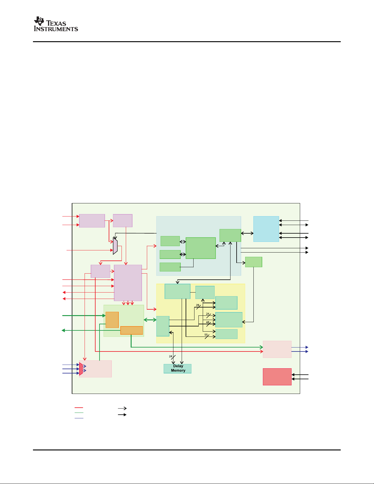
2 Functional Description
DSP Core
8051MicroprocessorCore
Oscillator
DPLL
Clock
Divider
512FsXTAL
MCLK_IN
512Fs
Slave
Master
Clock
Generation
Serial AudioPort
LRCLK_OUT
SCLK_OUT
LRCLK_IN
SCLK_IN
SDOUT1/2
TwoStereo
ADC
Three
Differential
Stereo
AnalogInputs
TwoStereo
DAC
TwoDifferential
Stereo Analog
Outputs
SCL1/SDA1
SCL2/SDA2
GPIO1/2
Master/Slave
256Fs
Power
Supply
AVDD
DVDD
128Fs
Volume
Update
Input
Cross
Bar
Mixer
OutputCross
BarMixer
SDIN1/2
Clocks
Legend
DigitalData
AnalogData
InternalConnection
External Connection
Control
Registers
External
RAM2K
Code
RAM16K
8-Bit
MCU
Internal
RAM256
DataRAM
1KUpperMem
768LowerMem
Coefficient
RAM 1.2K
Code
RAM 3K
DSP
Control
Memory
Interface
Data
Path
I2C
Control
Interface
TAS3204
AUDIO DSP
WITH ANALOG INTERFACE
SLES197 – APRIL 2007
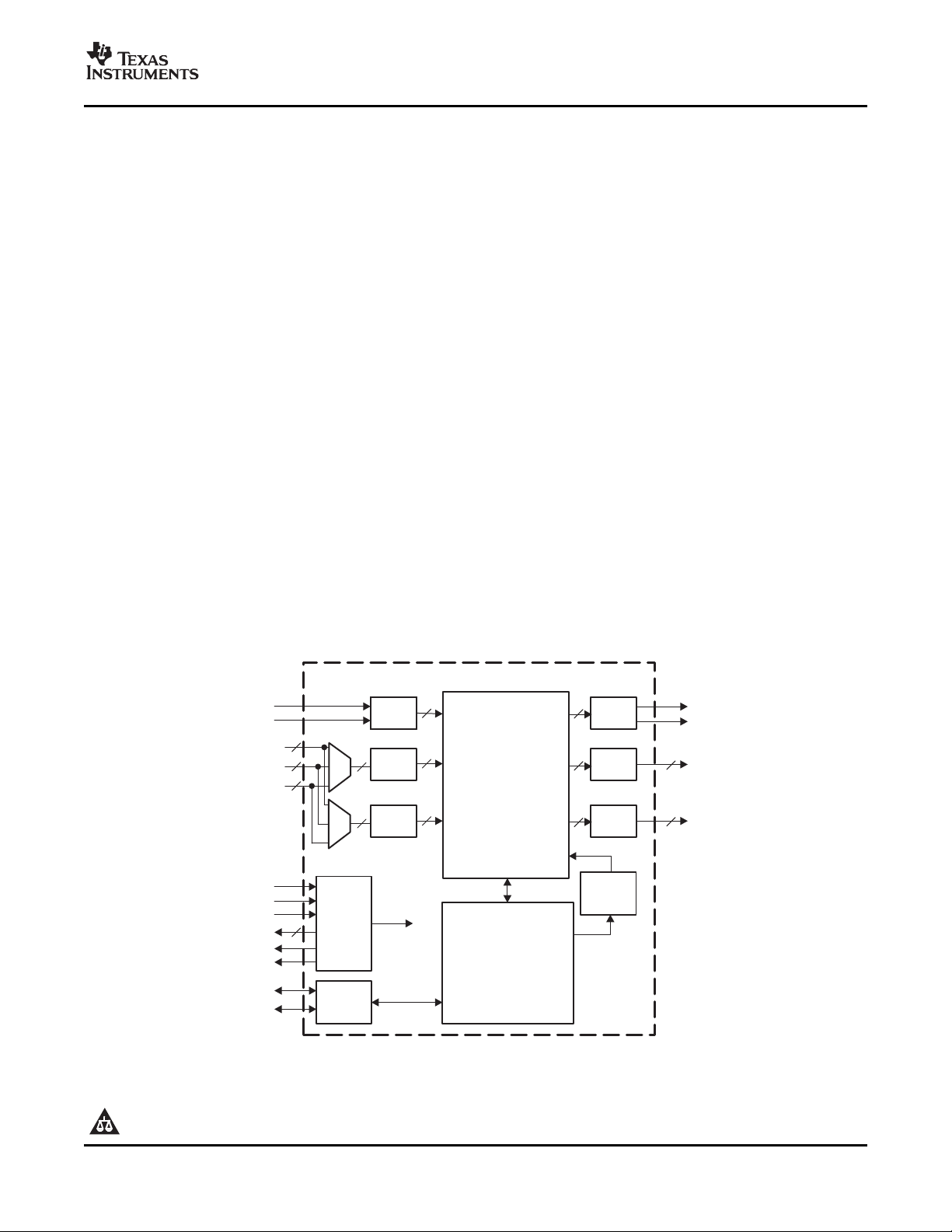
The TAS3204 is an audio system-on-a-chip (SOC) designed for mini/micro systems, multimedia-speaker,
and MP3 player docking systems. It includes analog interface functions: three multiplex (MUX) stereo
inputs with two stereo analog-to-digital converters (ADCs), two stereo digital-to-analog converters (DACs)
with analog outputs consisting of differential stereo line drivers. Four channels of serial digital audio
processing are also provided. The TAS3204 has a programmable audio digital signal processor (DSP) that
preserves high-quality audio by using a 48-bit data path, 28-bit filter coefficients, and a single cycle
28 × 48-bit multiplier. The programmability feature allows users to customize features in the DSP RAM.
The TAS3204 is composed of eight functional blocks:
1. Analog input/mux/stereo ADC
2. Two stereo DACs
3. Analog reference system
4. Power supply
5. Clocks, digital pll, and serial data interface
6. I2C control interface
7. 8051 microcontroller
8. Audio DSP – digital audio processing
Figure 2-1. Expanded Functional Block Diagram
Submit Documentation Feedback Functional Description 3
Page 4

www.ti.com
TAS3204
AUDIO DSP
WITH ANALOG INTERFACE
SLES197 – APRIL 2007
2.1 Analog Input/MUX/Stereo ADCs
These modules allow three differential analog stereo inputs to be sent to either of two ADCs to be
converted to digital data. The input multiplexers include a preamplifier. This amplifier is driving the ADCs,
and it is digitally controlled with changes synchronized with the sample clock of the ADC. Minimal
crosstalk between selected channels and unselected channels is maintained. When inputs are not needed
they are configured for minimal noise. Also included in this module are two fully differential over sampled
stereo ADCs. The ADCs are sigma-delta modulators with 256 times over-sampling ratio. Because of the
over-sampling nature of the audio ADCs and integrated digital decimation filters, requirements for analog
anti-aliasing filtering are relaxed. Filter performance for the ADCs are specified under physical
characteristics.
2.2 Stereo DACs
This module includes two stereo audio DACs, each of which consists of a digital interpolation filter, digital
sigma-delta modulator and an analog reconstruction filter. Each DAC can operate a maximum of 48 kHz.
Each DAC upsamples the incoming data by 128 and performs interpolation filtering and processing on this
data before conversion to a stereo analog output signal. The sigma-delta modulator always operates at a
rate of 128Fs, which ensures that quantization noise generated within the modulator stays low within the
frequency band below Fs/2.4 at all sample rates. The digital interpolation filters for interpolation from Fs to
8 × Fs are included in the audio DSP upper memory (reserved for analog processing), while interpolation
from 8 × Fs to 128Fs is done in a dedicated hardware sample and hold filter. The TAS3204 includes two
stereo line driver outputs. All line drivers are capable of driving up to a 10-k Ω load. Each stereo output can
be in power-down mode when not used. Popless operation is achieved by conforming to start and stop
sequences in the device controller code.
2.3 Analog Reference System
This module provides all internal references needed by the analog modules. It also provides bias currents
for all analog blocks. External decoupling capacitors are needed along with an external 1%-tolerance
resistor to set the internal bias currents. It includes a band-gap reference and several voltage buffers and
a tracking current reference. The TAS3204 also uses an internally generated mid supply that is used to
rereference all analog inputs and is present on all analog outputs. VMID is the analog mid supply and can
be used when buffered externally to rereference the analog inputs and outputs. The voltage reference
REXT requires a 22-k Ω 1% resistor to ground. The reference system can be powered down separately.
2.4 Power Supply
The power supply contains supply regulators that provide analog and digital regulated power for various
sections of the TAS3204. Only one external 3.3-V supply is required. All other voltages are generated on
chip from the external 3.3-V supply.
2.5 Clocks, Digital PLL, and Serial Data Interface
These modules provide the timing and serial data interface for the TAS3204. The clocking system for the
device is illustrated in Figure 2-2 . The TAS3204 can be either clock master or clock slave depending on
the configuration. However, master mode is the primary mode of operation.
Functional Description4 Submit Documentation Feedback
Page 5
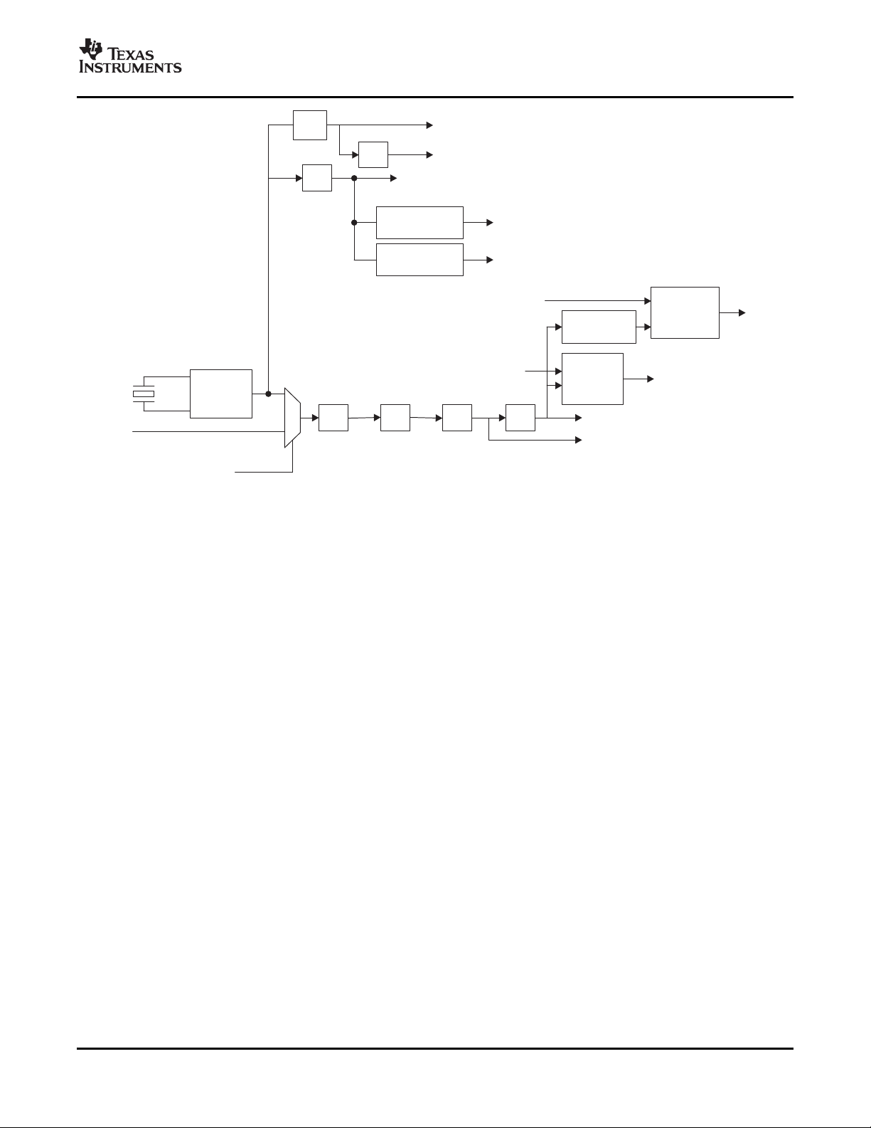
www.ti.com
DPLL
×5.5
÷4
135-MHz DCLK
Microprocessor Clock
MCLK_OUT
MCLK_OUT2
MCLK_OUT3
Programmable
Divider
÷2 ÷2 ÷2 ÷64
÷2
Programmable
Divider
Master/
Slave
LRCLK_OUT
SCLK_OUT
SDOUT
To DAP
Parallel
Data
SDIN
From DAP
Parallel
Data
LRCLK
Re-Creation
Serial
Audio Port
Receiver
Serial
Audio Port
Transmitter
256Fs 128Fs 64Fs
512Fs
Crystal
MCLKI
24.576 MHz
Oscillator
24.576 MHz
TAS3204
AUDIO DSP
WITH ANALOG INTERFACE
SLES197 – APRIL 2007
Figure 2-2. Clock Generation
DISCLAIMER: Analog performance is not ensured in slave mode, as the analog performance depends
upon the quality of the MCLK_IN. The TAS3204 is not robust with respect to MCLK_IN errors (glitches,
etc.); if the MCLK_IN frequency changes under operation, the device must be reset.
Master mode operation:
• External 512Fs crystal oscillator is used to generate all internal clocks plus all clocks for external
asynchronous sampling rate converter (ASRC) output (if external ASRC is present).
• LRCLK_OUT is fixed at 48 kHz (Fs).
• SCLK_OUT is fixed at 64Fs.
• MCLK_OUT is fixed at 256Fs. In master mode, the external ASRC converts incoming serial audio data
to 48-kHz sample rate synchronous to the internally generated serial audio data clocks.
• In master mode, all clocks generated for the TAS3204 are derived from the 24.576-MHz crystal. The
internal oscillator drives the crystal and generates the main clock to digital PLL (DPLL), master clock
outputs, 256Fs clock to the ADC, and 128Fs clock to the DAC. The DPLL generates internal clocks for
the DAP and the 8051 microprocessor.
Slave mode operation:
• MCLK_IN (512Fs), SCLK_IN (64Fs), and LRCLK_IN (Fs) are supplied externally. Clock generation is
similar to the master mode with the exception of the ADC and the DAC blocks. MCLK_IN signal is
divided down and sent directly to the ADC and the DAC blocks. Therefore, audio performance
depends on the MCLK_IN signal.
• DSP, MCU, and I2C clocks are still derived from external crystal oscillator.
• MCLK_OUT, SCLK_OUT, and LRCLK_OUT are passed through from clock inputs (MCLK_IN,
SCLK_IN, and LRCLK_IN).
• Internal analog clocks for ADC and DACs are derived from external MCLK_IN input, so analog
performance depends on MCLK_IN quality (i.e., jitter, phase noise, etc.). Degradation in analog
performance is to be expected.
Submit Documentation Feedback Functional Description 5
• Sample rate change/clock change
Page 6

www.ti.com
TAS3204
AUDIO DSP
WITH ANALOG INTERFACE
SLES197 – APRIL 2007
In slave mode, all incoming serial audio data must be synchronous to an incoming LRCLK_IN of 44.1 kHz
or 48 kHz.
2.6 I2C Control Interface
The TAS3204 has an I2C slave-only interface (SDA1 and SCL1) for receiving commands and providing
status to the system controller, and a separate master I2C interface (SDA2 and SCL2) to download
programs and data from external memory such as an EEPROM. See Section 6 for more information. I2C
interface is not 5-V tolerant.
2.7 8051 Microcontroller
The 8051 microcontroller receives and distributes I2C write data. It retrieves and outputs data as
requested from the I2C bus controller. It performs most processing tasks requiring multi-frame processing
cycles. The microprocessor has its own data RAM for storing intermediate values and queuing I2C
commands, a fixed boot program ROM, and a programmable RAM. The microprocessor's boot program
cannot be altered. The microcontroller has specialized hardware for a master and slave interface
operation, volume updates, and a programmable interval-timer interrupt.
– Sample rate change on the fly should be handled by customer system controller. The TAS3204
device does not include any internal clock error or click/pop detection/management.
– Customer-specific DAP filter coefficients must be uploaded by customer system controller on
changing sample rate.
2.8 Audio Digital Signal Processor Core
The audio digital signal processor core arithmetic unit is a fixed-point computational engine consisting of
an arithmetic unit and data and coefficient memory blocks. The audio processing structure, which can
include mixers, multiplexers, volume, bass and treble, equalizers, dynamic range compression, or
third-party algorithms, is running in the DAP. The 8051 microcontroller has access to DAP resources such
as coefficient RAM and is able to support the DAP with certain tasks; for example, a volume ramp. The
primary blocks of the audio DSP core are:
• 48-bit data path with 76-bit accumulator
• DSP controller
• Memory interface
• Coefficient RAM (1K × 28)
• Data RAM – 24-bit upper memory (1K × 24), 48-bit lower memory (768 × 48)
• Program RAM (3K × 55)
The DAP is discussed in detail in the following sections.
6 Functional Description Submit Documentation Feedback
Page 7
www.ti.com
PAG PACKAGE
(TOP VIEW)
1
2
3
4
5
6
7
8
9
10
11
12
13
14
15
16
48
47
46
45
44
43
42
41
40
39
38
37
36
35
34
33
17
18
19
20
21
22
23
24
25
26
27
28
29
30
31
32
64
63
62
61
60
59
58
57
56
55
54
53
52
51
50
49
I2C1_SCL
I2C1_SDA
GPIO2
GPIO1
MUTE
CS0
PDN
DVSS1
DVDD1
VR_PLL
AVSSI
AIN1LP
AIN1LM
AIN1RP
AIN1RM
AIN2LP
AIN2LM
AIN2RP
AIN2RM
AIN3LP
AIN3LM
AIN3RP
AIN3RM
A
VDD1
VMID
VREF
REXT
AVDD2
AOUT2LM
A
OUT2LP
AOUT2RM
AOUT2RP
MCLK_OUT1
MCLK_OUT2
MCLK_OUT3
DVDD2
DVSS2
MCLK_IN
XTAL_OUT
XTAL_IN
AVDD3
VR_ANA
AVSS_ESD
AVSSO
AOUT1RP
AOUT1RM
AOUT1LP
AOUT1LM
I2C2_SCL
I2C2_SDA
RESET
SDIN1/GPIO3
SDIN2/GPIO4
SCLK_IN
LRCLK_IN
DVDD3
DVSS3
VR_DIG
SDO1
SDO2
SCLK_OUT
LRCLK_OUT
RESER
VED
VREG_EN
TAS3204
AUDIO DSP
WITH ANALOG INTERFACE
SLES197 – APRIL 2007
3 Physical Characteristics
3.1 Terminal Assignments
3.2 Ordering Information
T
A
0 ° C to 70 ° C TAS3204PAG
PLASTIC 64-PIN PQFP (PN)
Submit Documentation Feedback Physical Characteristics 7
Page 8
www.ti.com
TAS3204
AUDIO DSP
WITH ANALOG INTERFACE
SLES197 – APRIL 2007
3.3 Terminal Descriptions
TERMINAL
NAME NO.
AIN1LM 13 Analog Input Pull to VMID
AIN1LP 12 Analog Input Analog input, channel 1, left, + input
AIN1RM 15 Analog Input Pull to VMID
AIN1RP 14 Analog Input Analog input, channel 1, right, + input
AIN2LM 17 Analog Input Pull to VMID
AIN2LP 16 Analog Input Analog input, channel 2, left, + input
AIN2RM 19 Analog Input Pull to VMID
AIN2RP 18 Analog Input Analog input, channel 2, right, + input
AIN3LM 21 Analog Input Pull to VMID
AIN3LP 20 Analog Input Analog input, channel 3, left, + input
AIN3RM 23 Analog Input Pull to VMID
AIN3RP 22 Analog Input Analog input, channel 3, right,+ input
AOUT1LM 33 Analog Output Analog output, channel 1, left, – output
AOUT1LP 34 Analog Output Analog output, channel 1, left, + output
AOUT1RM 35 Analog Output Analog output, channel 1, right, – output
AOUT1RP 36 Analog Output Analog output, channel 1, right, + output
AOUT2LM 29 Analog Output Analog output, channel 2, left, – output
AOUT2LP 30 Analog Output Analog output, channel 2, left, + output
AOUT2RM 31 Analog Output Analog output, channel 2, right, – output
AOUT2RP 32 Analog Output Analog output, channel 2, right,+ output
AVDD1 24 Power
AVSS1 11 Power Analog supply ground
AVDD2 28 Power
AVSS2 37 Power Analog supply ground
AVDD3 40 Power
AVSS3 38 Power Analog supply ground
CS0 6 Digital Input I2C secondary address
DVDD1 9 Power
DVSS1 8 Power Digital supply ground
DVDD2 45 Power
DVSS2 44 Power Digital supply ground
DVDD3 57 Power
DVSS3 56 Power Digital supply ground
GPIO1 4 Digital IO
GPIO2 3 Digital IO General-purpose I/O pin
I2C1_SCL 1 Digital Input
INPUT/ PULLUP/
OUTPUT
(1)
PULLDOWN
(2)
(3)
Analog input, channel 1, left, – input
(3)
Analog input, channel 1, right, – input
(3)
Analog input, channel 2, left, – input
(3)
Analog input, channel 2, right, – input
(3)
Analog input, channel 3, left, – input
(3)
Analog input, channel 3, right, – input
3.3-V analog power supply. This pin must be decoupled according to
good design practices.
3.3-V analog power supply. This pin must be decoupled according to
good design practices.
3.3-V analog power supply. This pin must be decoupled according to
good design practices.
3.3-V digital power supply. This pin must be decoupled according to
good design practices.
3.3-V digital power supply. This pin must be decoupled according to
good design practices.
3.3-V digital power supply. This pin must be decoupled according to
good design practices.
General-purpose I/O pin. When booting from internal ROM, the
TAS3204 streams audio when GPIO1 is low; otherwise it mutes.
Slave I2C serial control data interface input/output. Normally connected
to system micro.
DESCRIPTION
(1) I = input; O = output
(2) All pullups are 20- µ A weak pullups, and all pulldowns are 20- µ A weak pulldowns. The pullups and pulldowns are included to ensure
proper input logic levels if the terminals are left unconnected (pullups → logic 1 input; pulldowns → logic 0 input). Devices that drive
inputs with pullups must be able to sink 20 µ A while maintaining a logic-0 drive level. Devices that drive inputs with pulldowns must be
able to source 20 µ A while maintaining a logic-1 drive level.
(3) Pull to VMID when analog input is in single-ended mode.
Physical Characteristics8 Submit Documentation Feedback
Page 9
www.ti.com
TAS3204
AUDIO DSP
WITH ANALOG INTERFACE
SLES197 – APRIL 2007
TERMINAL
NAME NO.
I2C1_SDA 2 Digital I/O Slave I2C serial clock input. Normally connected to system micro.
I2C2_SCL 64 Digital Input
I2C2_SDA 63 Digital I/O Master I2C serial clock input. Normally connected to EEPROM.
LRCLK_IN 58 Digital Input Pulldown Serial data input left/right clock for I2S interface
LRCLK_OUT 51 Digital Output Serial data output left/right clock for I2S interface
MCLK_IN 43 Digital Input Pulldown
MCLK_OUT1 48 Digital Output 12.288 MHz clock output. This output is valid even when reset is LOW.
MCLK_OUT2 47 Digital Output in the range 0 to 255. Default value is 1.024 MHz. This output is valid
MCLK_OUT3 46 Digital Output in the range 0 to 255. Default value is 512 kHz. This output is valid
MUTE 5 Digital Input Pulldown
PDN 7 Digital Input
RESERVED 50 N/A Pulldown Connect to ground.
RESET 62 Digital Input Pullup
REXT 27 Analog Output
SCLK_IN 59 Digital Input Serial data input bit clock for I2S interface
SCLK_OUT 52 Digital Output Serial data output bit clock for I2S interface
SDIN1/GPIO3 61 Digital I/O Pullup Serial data input #1 for I2S interface or programmable for GPIO #3
SDIN2/GPIO4 60 Digital I/O Pullup Serial data input #2 for I2S interface or programmable for GPIO #4
SDOUT1 54 Digital Output Serial data output #1 for I2S interface
SDOUT2 53 Digital Output Serial data output #2 for I2S interface
VMID 25 Analog Output
VR_ANA 39 Power
VR_DIG 55 Power
VR_PLL 10 Power
VREF 26 Analog Output between this terminal and AVSS_PLL. This terminal must not be used
VREG_EN 49 Digital Input
XTAL_IN 41 Digital Input Crystal input. A 24.576-MHz (512Fs) crystal should be used.
XTAL_OUT 42 Digital Output Crystal output.
(4) If desired, low ESR capacitance values can be implemented by paralleling two or more ceramic capacitors of equal value. Paralleling
capacitors of equal value provide an extended high frequency supply decoupling.
INPUT/ PULLUP/
OUTPUT
(1)
PULLDOWN
(2)
Master I2C serial control data interface input/output. Normally
connected to EEPROM.
MCLK input is used in slave mode. MCLK_IN must be locked to
LRCLK_IN, and the frequency is 512Fs (24.576 MHz for 48-kHz Fs).
The frequency for this clock is 6.144 MHz/(n+1) where n is programable
even when reset is LOW.
The frequency for this clock is 512 kHz/(n+1) where n is programmable
even when reset is LOW.
This pin needs to be programmed as mute pin in the application code.
In has no function in default after reset.
Power down, active LOW. After successful boot, its function is defined
by the boot code.
System reset input, active low. A system reset is generated by applying
a logic LOW to this terminal.
Requires a 22-k Ω (1%) external resistor to ground to set analog
currents. Trace capacitance must be kept low.
Analog mid supply reference. This pin must be decoupled with a 0.1- µ F
low-ESR capacitor and an external 10- µ F filter cap.
Voltage reference for analog supply. A pin-out of the internally
regulated 1.8 V power. A 0.1- µ F low ESR capacitor and a 4.7- µ F filter
capacitor must be connected between this terminal and AVSS_PLL.
This terminal must not be used to power external devices.
Voltage reference for digital supply. A pin-out of the internally regulated
1.8 V power. A 0.1- µ F low ESR capacitor and a 4.7- µ F filter capacitor
must be connected between this terminal and DVSS. This terminal
must not be used to power external devices.
Voltage reference for DPLL supply. A pin-out of internally regulated
1.8-V power supply. A 0.1- µ F low-ESR capacitor and a 4.7- µ F filter
capacitor must be connected between this terminal and DVSS. This
terminal must not be used to power external devices.
Band gap output. A 0.1- µ F low ESR capacitor should be connected
to power external devices.
Voltage regulator enable. When enabled LOW, this input causes the
power-supply regulators to be enabled.
DESCRIPTION
(4)
(4)
(4)
(4)
(4)
Submit Documentation Feedback Physical Characteristics 9
Page 10

www.ti.com
TAS3204
AUDIO DSP
WITH ANALOG INTERFACE
SLES197 – APRIL 2007
3.4 Reset ( RESET) - Power-Up Sequence
The RESET pin is an asynchronous control signal that restores all TAS3204 components to the default
configuration. When a reset occurs, the audio DSP core is put into an idle state and the 8051 starts
initialization. A valid XTAL_IN must be present when clearing the RESET pin to initiate a device reset. A
reset can be initiated by applying a logic 0 on RESET.
As long as RESET is held LOW, the device is in the reset state. During reset, all I2C and serial data bus
operations are ignored. The I2C interface SCL and SDA lines go into a high-impedance state and remain
in that state until device initialization has completed.
The rising edge of the reset pulse begins the initialization housekeeping functions of clearing memory and
setting the default register values. Once these are complete, the TAS3204 enables its master I2C interface
and disables its slave I2C interface.
Using the master interface, the TAS3204 automatically tests to see if an external I2C EEPROM is at
address "1010x". The value x can be chip selects, other information, or don't care, depending on the
EEPROM selected.
If a memory is present and it contains the correct header information and one or more blocks of
program/memory data, the TAS3204 begins to load the program, coefficient and/or data memories from
the external EEPROM. If an external EEPROM is present, the download is considered complete when an
end of program header is read by the TAS3204. At this point, the TAS3204 disables the master I2C
interface, enable the slave I2C interface, and start normal operation. After a successful download, the
micro program counter is reset, and the downloaded micro and DAP application firmware controls
execution.
If no external EEPROM is present or if an error occurs during the EEPROM read, TAS3204 disables the
master I2C interface and enables the slave I2C interface initialization to load the slave default
configuration. In this default configuration, the TAS3204 streams audio from input to output if the GPIO1
pin is asserted LOW; if the GPIO1 pin is asserted HIGH, the ADC and the DAC are muted.
Note: The master and slave interfaces do not operate simultaneously.
3.5 Voltage Regulator Enable ( VREG_EN)
Setting the VREG_EN high shuts down all voltage regulators in the device. Internal register settings are
lost in this power down mode. A full power-up/reset/program-load sequence must be completed before the
device is operational.
3.6 Power-On Reset ( RESET)
On power up, it is recommended that the TAS3204 RESET be held LOW until DVDD has reached 3.3 V.
This can be done by programming the system controller or by using an external RC delay circuit. The
1-k Ω and 1- µ F values provide a delay of approximately 200 µ s. The values of R and C can be adjusted to
provide other delay values as necessary.
3.7 Power Down ( PDN)
The TAS3204 supports a number of power-down modes.
PDN can be used to put the device into power saving standby mode. PDN is user-firmware definable. Its
default configuration is to stop all clocks, power down all analog circuitry, and ramp down volume for all
digital inputs. This mode is used to minimize power consumption while preserving register settings. If there
is no EEPROM or if the EEPROM has an invalid image–i.e., an unsuccessful boot from the EEPROM–and
PDN is pulled low, the TAS3204 is in powerdown mode. After a successful boot, PDN is defined by the
boot code.
Physical Characteristics10 Submit Documentation Feedback
Page 11

www.ti.com
Individual power down DAC and ADC – Each stereo DAC and ADC can be powered down individually. To
avoid audible artifacts at the outputs, the sequences defined in the TI document TAS3108/TAS3108IA
Firmware Programmer's Guide (SLEU067 ) must be followed. The control signals for these operations are
defined as ESFR. The feature is made available to the board controller via the I2C interface.
Power down of analog reference – The analog reference can be powered down if all DAC and ADC are
powered down. This operation is handled by the device controller through the ESFRs, and is made
available to the board controller via the I2C interface.
3.8 I2C Bus Control (CS0)
The TAS3204 has a control to specify the slave and master I2C address. This control permits up to two
TAS3204 devices to be placed in a system without external logic. GPIO pins are level sensitive. They are
not edge triggered.
See Section 6.3 for a complete description of this pin.
3.9 Programmable I/O (GPIO)
The TAS3204 has four GPIO pins and two general purpose input pins that are 8051 firmware
programmable.
TAS3204
AUDIO DSP
WITH ANALOG INTERFACE
SLES197 – APRIL 2007
GPIO1 and GPIO2 pins are single function I/O pins. Upon power up, GPIO1 is an input. If there is an
unsuccessful boot and GPIO1 is pulled high externally, the DAC output is disabled. If there is an
unsuccessful boot and the GPIO1 is pulled low externally, the DAC output is enabled. If there is a
successful boot, GPIO1 is pulled low by the internal microprocessor, and its function is defined by the boot
code in the EEPROM.
GPIO3 and GPIO4 pins are dual function I/O pins. These pins can be used as SDIN1 and SDIN2
respectively.
Mute and power down functions have to be programmed in the EEPROM boot code. These are
general-purpose input pins and can be programmed for functions other than mute and power down.
For more information, see the Texas Instruments document TAS3108/TAS3108IA Firmware Programmer's
Guide (SLEU067 ).
3.9.1 No EEPROM is Present or a Memory Error Occurs
Following reset or power-up initialization with the EEPROM not present or if a memory error occurs, the
TAS3204 is in one of two modes, depending on the setting of GPIO1.
• GPIO1 is logic HIGH
With GPIO1 held HIGH during initialization, the TAS3204 comes up in the default configuration with the
serial data outputs not active. Once the TAS3204 has completed the default initialization procedure,
after the status register is updated and the I2C slave interface is enabled, then GPIO1 is an output and
is driven LOW. Following the HIGH-to-LOW transition of the GPIO pin, the system controller can
access the TAS3204 through the I2C interface and read the status register to determine the load
status.
If a memory-read error occurs, the TAS3204 reports the error in the status register (I2C subaddress
0x02).
• GPIO1 is logic LOW
With GPIO1 held LOW during initialization, the TAS3204 comes up in an I/O test configuration. In this
case, once the TAS3204 completes its default test initialization procedure, the status register is
updated, the I2C slave interface is enabled, and the TAS3204 streams audio unaltered from input to
output as SDIN1 to SDOUT1, SDIN2 to SDOUT2, etc.
Submit Documentation Feedback Physical Characteristics 11
Page 12
www.ti.com
TAS3204
AUDIO DSP
WITH ANALOG INTERFACE
SLES197 – APRIL 2007
In this configuration, GPIO1 is an output signal that is driven LOW. If the external logic is no longer
driving GPIO1 low after the load has completed (~100 ms following a reset if no EEPROM is present),
the state of GPIO1 can be observed.
Then the system controller can access the TAS3204 through the I2C interface and read the status
register to determine the load status.
If the GPIO1 state is not observed, the only indication that the device has completed its initialization
procedure is the fact that the TAS3204 streams audio and the I2C slave interface has been enabled.
3.9.2 GPIO Pin Function After Device Is Programmed
Once the TAS3204 has been programmed, either through a successful boot load or via slave I2C
download, the operation of GPIO can be programmed to be an input and/or output.
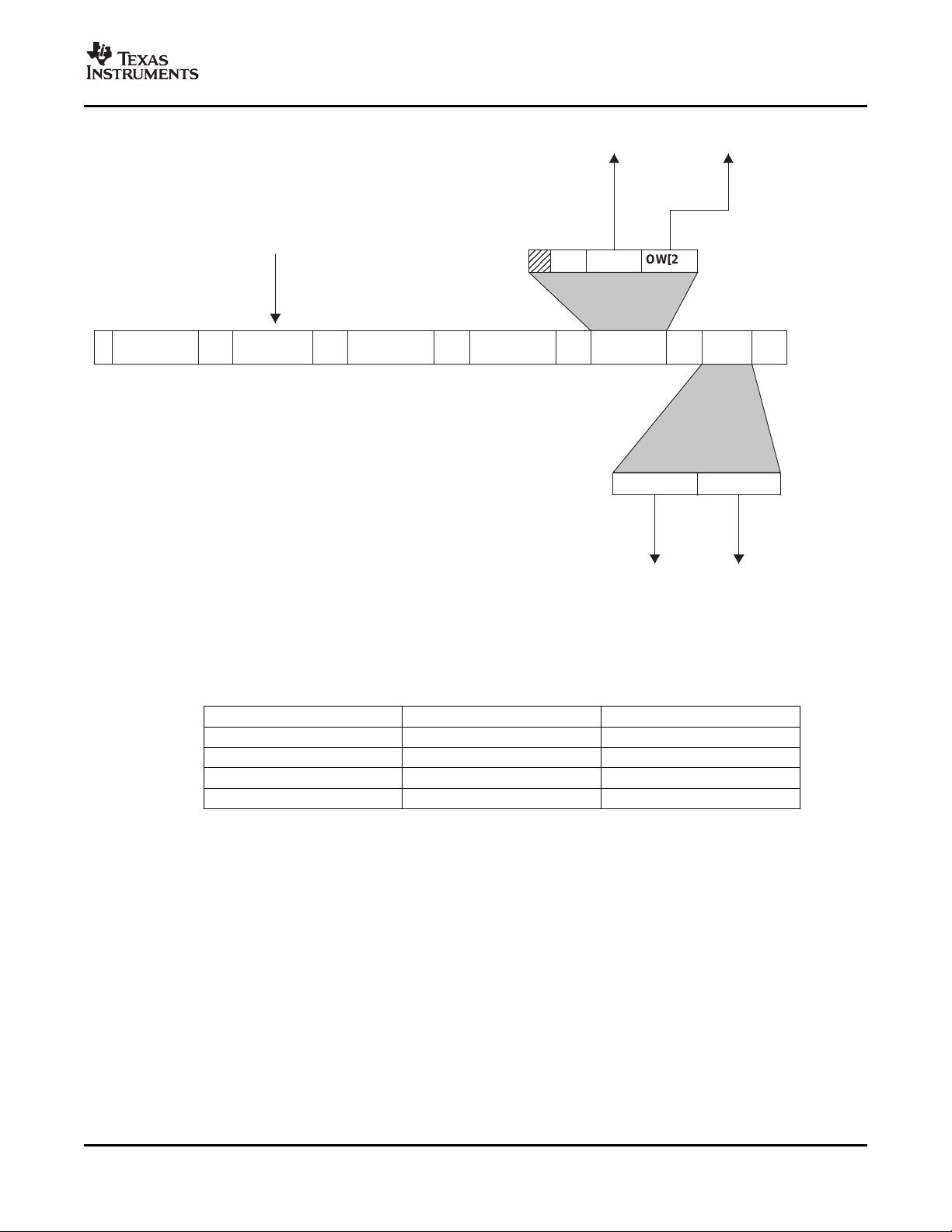
3.10 Input and Output Serial Audio Ports
Serial data is input on SDIN1/SDIN2 on the TAS3204, allowing up to four channels of digital audio input.
The TAS3204 supports serial data in 16-, 20-, or 24-bit data in left, right, and I2S serial data formats. The
parameters for the clock and serial data interface input formats are I2C configurable.
Serial data is output on SDOUT1 and SDOUT2, allowing up to four channels of digital audio output.
SDOUT port supports the same formats as the SDIN port. Output data rate is the same data rate as the
input. The SDOUT output uses the SCLK_OUT and LRCLK_OUT signals to provide synchronization.
The TAS3204 supported data formats are listed in Table 3-1 .
Table 3-1. Supported Data Formats
Input SAP (SDIN1, SDIN2) Output SAP (SDOUT1, SDOUT2)
2-channel I2S 2-channel I2S
2-channel left-justified 2-channel left-justified
2-channel right-justified 2-channel right-justified
Table 3-2. Serial Data Input and Output Formats
Mode Control Control Serial Format Word Lengths Rates SCLK
2-channel 0001 0001 Right-justified 16, 20, 24 32–48 3.072
Input Output Data MAX
IM[3:0] OM[3:0] (kHz) (MHz)
0000 0000 Left-justified 16, 20, 24
0010 0010 I2S 16, 20, 24
Physical Characteristics12 Submit Documentation Feedback
Page 13
www.ti.com
0x00
DWFMT (Data Word Format)
AckIOMAck
OW[2:0]
15
IW[2:0]
0
XX
14 13 11 10 8
7
DWFMT
815
AckxxxxxxxxAckSubaddrAckSlave AddrS
2431
OM[3:0]IM[3:0]
7 4 3 0
xxxxxxxxAck
1623
Output Port
Format
Input Port
Format
Input Port
Word Size
Output Port
Word Size
R0003-01
TAS3204
AUDIO DSP
WITH ANALOG INTERFACE
SLES197 – APRIL 2007
Figure 3-1. Serial Data Controls
Table 3-3. Serial Data Input and Output Data Word Sizes
IW1, OW1 IW0, OW0 FORMAT
0 0 Reserved
0 1 16-bit data
1 0 20-bit data
1 1 24-bit data
Following a reset, ensure that the clock register (0x00) is written before performing volume, treble, or bass
updates.
Commands to reconfigure the SAP can be accompanied by mute and unmute commands for quiet
operation. However, care must be taken to ensure that the mute command has completed before the SAP
is commanded to reconfigure. Similarly, the TAS3204 should not be commanded to unmute until after the
SAP has completed a reconfiguration. The reason for this is that an SAP configuration change while a
volume or bass or treble update is taking place can cause the update not to be completed properly.
When the TAS3204 is transmitting serial data, it uses the negative edge of SCLK to output a new data bit.
The TAS3204 samples incoming serial data on the rising edge of SCLK.
Submit Documentation Feedback Physical Characteristics 13
Page 14
www.ti.com
23 22
SCLK
32 Clks
LRCLK (Note Reversed Phase) Left Channel
24-Bit Mode
9 8 5 4 1 0
19 18
20-Bit Mode
5 4 1 0
16-Bit Mode
1 015 14
MSB LSB
23 22
SCLK
32 Clks
Right Channel
9 8 5 4 1 0
19 18 5 4 1 0
1 015 14
MSB LSB
2-Channel I2S (Philips Format) Stereo Input/Output
T0034-04
TAS3204
AUDIO DSP
WITH ANALOG INTERFACE
SLES197 – APRIL 2007
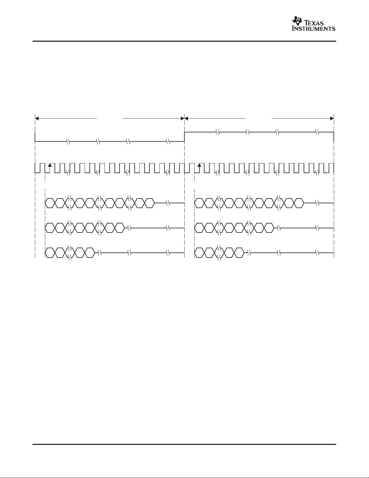
3.10.1 2-Channel I2S Timing
In 2-channel I2S timing, LRCLK is LOW when left-channel data is transmitted and HIGH when
right-channel data is transmitted. SCLK is a bit clock running at 64 × fSwhich clocks in each bit of the
data. There is a delay of one bit clock from the time the LRCLK signal changes state to the first bit of data
on the data lines. The data is written MSB first and is valid on the rising edge of the bit clock. The
TAS3204 masks unused trailing data-bit positions.
14 Physical Characteristics Submit Documentation Feedback
Figure 3-2. I2S 64f
Format
S
Page 15
www.ti.com
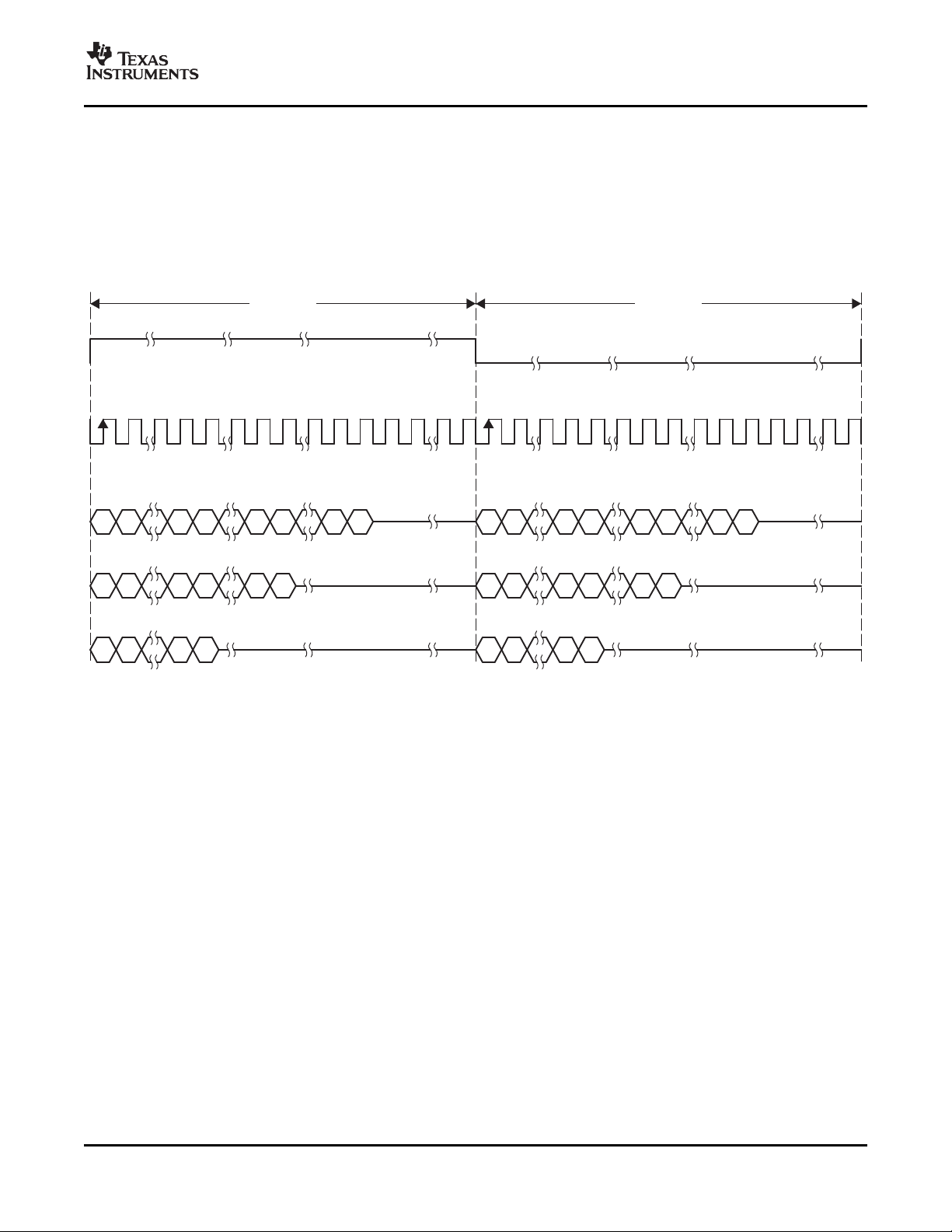
3.10.2 2-Channel Left-Justified Timing
23 22
SCLK
32 Clks
LRCLK
Left Channel
24-Bit Mode
9 8 5 4 1 0
MSB LSB
23 22
32 Clks
LRCLK
Right Channel
9 8 5 4 1 0
MSB LSB
18
20-Bit Mode
5 4 1 019
14
16-Bit Mode
1 015
18 5 4 1 019
14 1 015
2-Channel Left-Justified Stereo Input
T0034-02
In 2-channel left-justified timing, LRCLK is HIGH when left-channel data is transmitted and LOW when
right-channel data is transmitted. SCLK is a bit clock running at 64 × fS, which clocks in each bit of the
data. The first bit of data appears on the data lines at the same time LRCLK toggles. The data is written
MSB first and is valid on the rising edge of the bit clock. The TAS3204 masks unused trailing data-bit
positions.
TAS3204
AUDIO DSP
WITH ANALOG INTERFACE
SLES197 – APRIL 2007
Figure 3-3. Left-Justified 64f
Submit Documentation Feedback Physical Characteristics 15
Format
S
Page 16
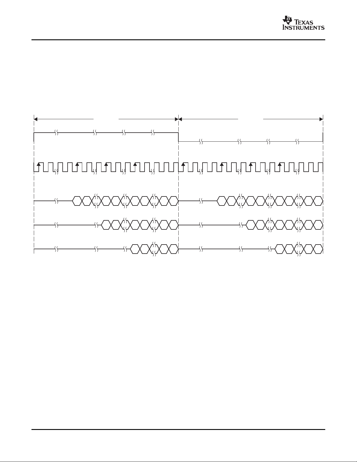
www.ti.com
23 22
SCLK
32 Clks
LRCLK
Left Channel
24-Bit Mode
19 18 15 14 1 0
19 18
20-Bit Mode
15 14 1 0
16-Bit Mode
1 015 14
MSB LSB
2-Channel Right-Justified (Sony Format) Stereo Input
23 22
32 Clks
Right Channel
19 18 15 14 1 0
19 18 15 14 1 0
1 015 14
MSB LSB
T0034-03
TAS3204
AUDIO DSP
WITH ANALOG INTERFACE
SLES197 – APRIL 2007
3.10.3 2-Channel Right-Justified Timing
In 2-channel right-justified (RJ) timing, LRCLK is HIGH when left-channel data is transmitted and LOW
when right-channel data is transmitted. SCLK is a bit clock running at 64 × fSwhich clocks in each bit of
the data. The first bit of data appears on the data lines 8 bit-clock periods (for 24-bit data) after LRCLK
toggles. In the RJ mode, the last bit clock before LRCLK transitions always clocks the LSB of data. The
data is written MSB first and is valid on the rising edge of the bit clock. The TAS3204 masks unused
leading data-bit positions.
Figure 3-4. Right-Justified 64f
3.10.4 SAP Input to SAP Output—Processing Flow
All SAP data format options other than I2S result in a two-sample delay from input to output. If I2S
formatting is used for both the input SAP and the output SAP, the polarity of LRCLK must be inverted.
However, if I2S format conversions are performed between input and output, the delay becomes either 1.5
samples or 2.5 samples, depending on the processing clock frequency selected for the audio DSP core
relative to the sample rate of the incoming data.
The I2S format uses the falling edge of LRCLK to begin a sample period, whereas all other formats use
the rising edge of LRCLK to begin a sample period. This means that the input SAP and audio DSP core
operate on sample windows that are 180 ° out of phase with respect to the sample window used by the
output SAP. This phase difference results in the output SAP outputting a new data sample at the midpoint
of the sample period used by the audio DSP core to process the data. If the processing cycle completes
all processing tasks before the midpoint of the processing sample period, the output SAP outputs this
processed data. However, if the processing time extends past the midpoint of the processing sample
period, the output SAP outputs the data processed during the previous processing sample period. In the
former case, the delay from input to output is 1.5 samples. In the latter case, the delay from input to output
is 2.5 samples.
Physical Characteristics16 Submit Documentation Feedback
Format
S
Page 17

www.ti.com
TAS3204
AUDIO DSP
WITH ANALOG INTERFACE
SLES197 – APRIL 2007
The delay from input to output can thus be either 1.5 or 2.5 sample times when data format conversions
are performed that involve the I2S format. However, which delay time is obtained for a particular
application is determinable and fixed for that application, providing care is taken in the selection of
MCLK_IN/XTAL_IN with respect to the incoming sample clock, LRCLK.
Submit Documentation Feedback Physical Characteristics 17
Page 18

www.ti.com
TAS3204
AUDIO DSP
WITH ANALOG INTERFACE
SLES197 – APRIL 2007
4 Algorithm and Software Development Tools for TAS3204
The TAS3204 algorithm and software development tool set is a combination of classical development
tools and graphical development tools. The tool set is used to build, debug, and execute programs in both
the audio DSP and 8051 sections of the TAS3204.
Classical development tooling includes text editors, compilers, assemblers, simulators, and source-level
debuggers. The 8051 can be programmed exclusively in ANSI C.
The 8051 tool set is an off-the-shelf tool set, with modifications as specified in this document. The 8051
tool set is a complete environment with an IDE, editor, compiler, debugger, and simulator.
The audio DSP core is programmed exclusively in assembly. The audio DSP tool set is a complete
environment with an IDE, context-sensitive editor, assembler, and simulator/debugger.
Graphical development tooling provides a means of programming the audio DSP core and 8051 through a
graphical drag-and-drop interface using modular audio software components from a component library.
The graphical tooling produces audio DSP assembly and 8051 ANSI C code as well as coefficients and
data. The classical tools can also be used to produce the executable code.
In addition to building applications, the tool set supports the debug and execution of audio DSP and 8051
code on both simulators and EVM hardware.
18 Algorithm and Software Development Tools for TAS3204 Submit Documentation Feedback
Page 19

www.ti.com
TAS3204
AUDIO DSP
WITH ANALOG INTERFACE
SLES197 – APRIL 2007
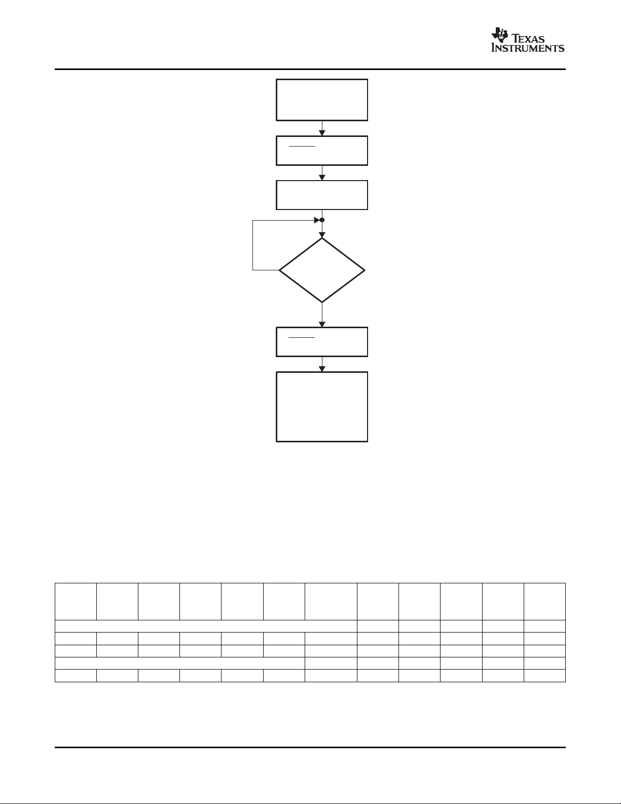
5 Clock Controls
Clock management for the TAS3204 consists of two control structures:
• Master clock management
– Oversees the selection of the clock frequencies for the 8051 microprocessor, the I2C controller, and
the audio DSP core
– The master clock (MCLK_IN or XTAL_IN) is the source for these clocks.
– In most applications, the master clock drives an on-chip digital phase-locked loop (DPLL), and the
DPLL output drives the microprocessor and audio DSP clocks.
– Also available is the DPLL bypass mode, in which the high-speed master clock directly drives the
microprocessor and audio DSP clocks.
• Serial audio port (SAP) clock management
– Oversees SAP master/slave mode
– Controls output of SCLKOUT, and LRCLK in the SAP master mode
Input pin MCLK_IN or XTAL_IN provides the master clock for the TAS3204. Within the TAS3204, these
two inputs are combined by an OR gate and, thus, only one of these two sources can be active at any one
time. The source that is not active must be logic 0.
The TAS3204 only supports dynamic sample-rate changes between any of the supported sample
frequencies when a fixed-frequency master clock is provided. During dynamic sample-rate changes, the
TAS3204 remains in normal operation and the register contents are preserved. To avoid producing audio
artifacts during the sample-rate changes, a volume or mute control can be included in the application
firmware that mutes the output signal during the sample-rate change. The fixed-frequency clock can be
provided by a crystal attached to XTAL_IN and XTAL_OUT or an external 3.3-V fixed-frequency TTL
source attached to MCLK_IN.
When the TAS3204 is used in a system in which the master clock frequency (f
TAS3204 must be reset during the frequency change. In these cases, the procedure shown in Figure 5-1
should be used.
) can change, the
MCLK
Submit Documentation Feedback Clock Controls 19
Page 20
www.ti.com
Are
Clocks
Stable?
No
Yes
RESET Pin = Low
Enable Mute and
Wait for Completion
Change f
MCLK
RESET Pin = High
After
TAS3204
Initializes,
Re-initialize
I C Registers
2
TAS3204
AUDIO DSP
WITH ANALOG INTERFACE
SLES197 – APRIL 2007
FSSample Ch Per LRCLK Ch Per LRCLK PLL F
Rate (kHz) SDIN Ratio SDOUT (FS) Multiplier (MHz)
20 Clock Controls Submit Documentation Feedback
Figure 5-1. Master Clock Frequency (f
) Change Procedure
MCLK
When the serial audio port (SAP) is in the master mode, the SAP uses the XTAL_IN master clock to drive
the serial port clocks SCLK_OUT and LRCLK. When the SAP is in the slave mode, MCLK_IN, SCLK_IN,
and LRCLK_IN are input clocks. SCLK_OUT and LRCLK_OUT are derived from SCLK_IN and
LRCLK_IN, respectively.
See Clock Register (0x00), Section 9.1 , for information on programming the clock register.
Table 5-1. TAS3204 MCLK and LRCLK Common Values (MCLK = 24.576 MHz or MCLK = 22.579 MHz)
MCLK/
44.1 2 512 22.579 64 2.822 64 2 64 5.5 124.2 2816
48 2 256 24.576 64 3.072 64 2 64 5.5 135.2 2816
Master Mode, 2 Channels In, 2 Channels Out
48 2 256 24.576 N/A N/A 64 2 64 5.5 135.2 2816
( × fS)
Slave Mode, 2 Channels In, 2 Channels Out
MCLK SCLKIN SCLK_IN SCLK_OUT
Freq Rate Freq Rate f
(MHz) ( × fS) (MHz) ( × fS)
DSPCLK
/f
DSPCLK
S
Page 21
www.ti.com
6 Microprocessor Controller
The 8051 microprocessor receives and distributes I2C write data, retrieves and outputs to the I2C bus
controllers the required I2C read data, and participates in most processing tasks requiring multiframe
processing cycles. The microprocessor has its own data RAM for storing intermediate values and queuing
I2C commands, a fixed boot-program ROM, and a program RAM. The microprocessor boot program
cannot be altered. The microprocessor controller has specialized hardware for master and slave interface
operation, volume updates, and a programmable interval timer interrupt. For more information see the
TAS3108/TAS3108IA Firmware Programmer's Guide (SLEU067 ).
The TAS3204 has a slave-only I2C interface that is compatible with the Inter IC (I2C) bus protocol and
supports both 100-kbps and 400-kbps data-transfer rates for multiple 4-byte write and read operations
(maximum is 20 bytes). The slave I2C control interface is used to program the registers of the device and
to read device status.
The TAS3204 also has a master-only I2C interface that is compatible with the I2C bus protocol and
supports 375-kbps data transfer rates for multiple 4-byte write and read operations (maximum is 20 bytes).
The master I2C interface is used to load program and data from an external I2C EEPROM.
On power up of the TAS3204, the slave interface is disabled and the master interface is enabled.
Following a reset, the TAS3204 disables the slave interface and enables the master interface. Using the
master interface, the TAS3204 automatically tests to see if an I2C EEPROM is at address 1010x. The
value x can be chip select, other information, or don’t cares, depending on the EEPROM selected. If a
memory is present and it contains the correct header information and one or more blocks of
program/memory data, the TAS3204 loads the program, coefficient, and/or data memories from the
EEPROM. If a memory is present, the download is complete when a header is read that has a zero-length
data segment. At this point, the TAS3204 disables the master I2C interface, enables the slave I2C
interface, and starts normal operation.
TAS3204
AUDIO DSP
WITH ANALOG INTERFACE
SLES197 – APRIL 2007
If no memory is present or if an error occurred during the EEPROM read, TAS3204 disables the master
I2C interface, enables the slave I2C interface, and loads the unprogrammed default configuration. In this
default configuration, the TAS3204 streams audio from input to output if the GPIO pin is LOW. The master
and slave interfaces do not operate simultaneously.
In the slave mode, the I2C bus is used to:
• Load the program and coefficient data
– Microprocessor program memory
– Microprocessor extended memory
– Audio DSP core program memory
– Audio DSP core coefficient memory
– Audio DSP core data memory
• Update coefficient and other control values
• Read status flags
Once the microprocessor program memory has been loaded, it cannot be updated until the TAS3204 has
been reset.
The master and slave modes do not operate simultaneously.
When acting as an I2C master, the data transfer rate is fixed at 375 kHz, assuming MCLK_IN or
XTAL_IN = 24.576 MHz.
When acting as an I2C slave, the data transfer rate is determined by the master device on the bus.
The I2C communication protocol for the I2C slave mode is shown in Figure 6-1 .
Submit Documentation Feedback Microprocessor Controller 21
Page 22

www.ti.com
SDA
SCL
0S
Start
(By Master)
Slave Address
(By Master)
0 1 1 0 1
C
S
0
Read or Write
(By Master)
R
/
W
A
C
K
M
S
B
Acknowledge
(By TAS3204)
L
S
B
Data Byte
(By Transmitter)
A
C
K
Acknowledge
(By Receiver)
M
S
B
L
S
B
Data Byte
(By Transmitter)
A
C
K
Acknowledge
(By Receiver)
S
Stop
(By Master)
MSB MSB-1 MSB-2 LSB
Start Condition
SDA ↓While SCL = 1
Stop Condition
SDA ↑While SCL = 1
(1)
TAS3204
AUDIO DSP
WITH ANALOG INTERFACE
SLES197 – APRIL 2007
Figure 6-1. I2C Slave-Mode Communication Protocol
6.1 8051 Microprocessor Addressing Mode
The 256 bytes of internal data memory address space is accessible using indirect addressing instructions
(including stack operations). However, only the lower 128 bytes are accessible using direct addressing.
The upper 128 bytes of direct address Data Memory space are used to access Extended Special Function
Registers (ESFRs).
6.1.1 Register Banks
There are four directly addressable register banks, only one of which may be selected at one time. The
register banks occupy Internal Data Memory addresses from 00 hex to 1F hex.
6.1.2 Bit Addressing
The 16 bytes of Internal Data Memory that occupy addresses from 20 hex to 2F hex are bit addressable.
SFRs that have addresses of the form 1XXXX000 binary are also bit addressable.
6.1.3 External Data Memory
External data memory occupies a 2K × 8 address space. This space contains the External Special
Function Data Registers (ESFRs). The ESFR permit access and control of the hardware features and
internal interfaces of the TAS3204.
Microprocessor Controller22 Submit Documentation Feedback
Page 23

www.ti.com
6.1.4 Extended Special Function Registers
Address
Decoder
D
WE
CCLK
D
WE
8051 MCU
DESTIN_DO
DESTIN_A
SFRWE
SFRWA
ESFRDI
Internal
Data
Memory
Bus
Control Out
Control In
CCLK
CCLK
ESFRs provide signals needed for the M8051 to control the different blocks in the device. ESFR is an
extension to the M8051. Figure 6-2 shows how these registers are arranged.
TAS3204
AUDIO DSP
WITH ANALOG INTERFACE
SLES197 – APRIL 2007
Figure 6-2. Extended Special Function Registers
6.1.5 Memory Mapped Registers for DAP Data Memory
The following memory mapped registers are used for communication with the digital audio processor.
Table 6-1. Memory Mapped Registers
Address Register Comment
0x0300 Dither Seed Sets the dither seed value
0x0301 PC Start Sets the starting address of the
0x0302 Reserved Reserved
DAP
Note that TAS3204 has the same memory mapped registers distinction of upper and lower memory for
these registers.
6.2 General I2C Operations
The I2C bus employs two signals, SDA (data) and SCL (clock), to communicate between integrated
circuits in a system. Data is transferred on the bus serially one bit at a time. The address and data are
transferred in byte (8-bit) format with the most-significant bit (MSB) transferred first. In addition, each byte
transferred on the bus is acknowledged by the receiving device with an acknowledge bit. Each transfer
operation begins with the master device driving a start condition on the bus and ends with the master
device driving a stop condition on the bus. The bus uses transitions on the data terminal (SDA) while the
clock is HIGH to indicate a start and stop conditions. A HIGH-to-LOW transition on SDA indicates a start,
and a LOW-to-HIGH transition indicates a stop. Normal data bit transitions must occur within the low time
of the clock period. The master generates the 7-bit slave address and the read/write (R/ W) bit to open
Submit Documentation Feedback Microprocessor Controller 23
communication with another device and then waits for an acknowledge condition. The slave holds SDA
LOW during acknowledge clock period to indicate an acknowledgement. When this occurs, the master
transmits the next byte of the sequence. Each device is addressed by a unique 7-bit slave address plus
R/ W bit (one byte). All compatible devices share the same signals via a bidirectional bus using a
wired-AND connection. An external pullup resistor must be used for the SDA and SCL signals to set the
HIGH level for the bus.
Page 24

www.ti.com
TAS3204
Address
TAS3204
Address
TAS3204
Address
Acknowledge
(By TAS3204)
Acknowledge
(By TAS3204)
Acknowledge
(By TAS3204)
Acknowledge
(By TAS3204)
Acknowledge
(By TAS3204)
Acknowledge
(By TAS3204)
Acknowledge
(By TAS3204)
Data
(By TAS3204)
TAS3204
Subaddress
(By Master)
TAS3204
Subaddress
(By Master)
Data
(By TAS3204)
Acknowledge
(By TAS3204)
TAS3204
AUDIO DSP
WITH ANALOG INTERFACE
SLES197 – APRIL 2007
There is no limit on the number of bytes that can be transmitted between start and stop conditions. When
the last word transfers, the master generates a stop condition to release the bus. Figure 6-3 shows the
TAS3204 read and write operation sequences.
As shown in Figure 6-3 , an I2C read transaction requires that the master device first issue a write
transaction to give the TAS3204 the subaddress to be used in the read transaction that follows. This
subaddress assignment write transaction is then followed by the read transaction. For write transactions,
the subaddress is supplied in the first byte of data written, and this byte is followed by the data to be
written. For I2C write transactions, the subaddress must always be included in the data written. There
cannot be a separate write transaction to supply the subaddress, as was required for read transactions. If
a subaddress-assignment-only write transaction is followed by a second write transaction supplying the
data, erroneous behavior results. The first byte in the second write transaction is interpreted by the
TAS3204 as another subaddress replacing the one previously written.
6.3 I2C Slave Mode Operation
The I2C slave mode is the mode that is used to change configuration parameters during operation and to
perform program and coefficient downloads from a master device. The coefficient download operation in
slave mode can be used to replace the I2C master-mode EEPROM download. The TAS3204 supports
both random and sequential I2C transactions. The TAS3204 I2C slave address is 011010xy, where the first
six bits are the TAS3204 device address and bit x is CS0, which is set by the TAS3204 internal
microprocessor at power up. Bit y is the R/ W bit. The pulldown resistance of CS0 creates a default 00
address when no connection is made to the pin. Table 6-1 and Table 6-3 show all the legal addresses for
I2C slave and master modes.
The number of data bytes plus the two bytes checksum must be evenly divisible by the word size.
The size field is equal to (header + payload + end checksum).
Microprocessor Controller24 Submit Documentation Feedback
Figure 6-3. I2C Subaddress Access Protocol
Page 25

www.ti.com
TAS3204
AUDIO DSP
WITH ANALOG INTERFACE
SLES197 – APRIL 2007
The checksum is contained in the last two data transfer bytes. These are bytes 7 and 8. On single word
transfers (DAP data, DAP instruction), the checksum is always contained in a 8 byte frame that follows the
last data word, last two bytes. For multiword data register transfers data (micro program, micro external
data, and coefficient RAM), the checksum is included in the same byte transfer as data. To meet the
requirement above, the number of words that are transferred contain modulo 8 + 6 in the case of micro
program and data memory, and modulo 2 + 1 in the case of coefficient memory. When the slave I2C
download is used to replace or update sections of micro program, micro data, or DAP coefficient memory,
it is necessary to take these transfer size restrictions into consideration when determining program, data,
and coefficient placements.
The multi word transfers always store first word on the bus at a lower RAM address and increment such
that the last word in the transfer is stored with the highest target RAM address. Consecutive I2C frame
transfers increment target address such that the data in the last transfer is last in target memory address
space.
When the first I2C slave download register is written by the system controlle, the TAS3204 updates the
status register by setting a error bit to indicate an error for the memory type that is being loaded. This
error bit is reset when the operation complete and a valid checksum has been received. For example
when the micro program memory is being loaded, the TAS3204 sets a micro program memory error
indication in the status register at the start of the sequence. When the last byte of the micro program
memory and checksum is received, the TAS3204 clears the micro program memory error indication. This
enables the TAS3204 to preserve any error status indications that occur as a result of incomplete
transfers of data/ checksum error during a series of data and program memory load operations.
The checksum is always contained in the last two bytes of the data block. The I2C slave download is
terminated when a termination header with a zero-length byte-count file is received.
The status register always reflects status of EEPROM boot attempts, unless the user writes to the slave
control register. A write to the slave boot control register causes the EEPROM status register to reflect
slave boot attempt status.
NOTE
Once the micro program memory has been loaded, further updates to this memory are
prohibited until the device is reset. The TAS3204 I2C block does respond to the broadcast
address (00h).
Table 6-2. Slave Addresses
Base Address CS0 R/ W Slave Address
0110 10 0 0 0x68
0110 10 0 1 0x69
0110 10 1 0 0x6A
0110 10 1 1 0x6B
Submit Documentation Feedback Microprocessor Controller 25
Page 26

www.ti.com
TAS3204
AUDIO DSP
WITH ANALOG INTERFACE
SLES197 – APRIL 2007
The following is an example use of the I2C master address to access an external EEPROM. The TAS3204
can address up to two EEPROMs depending on the state of CS0. Initially, the TAS3204 comes up in I2C
master mode. If it finds a memory such as the 24C512 EEPROM, it reads the headers and data as
previously described. In this I2C master mode, the TAS3204 addresses the EEPROMs as shown in
Table 6-4 and Table 6-5 .
Table 6-3. Master Addresses
Base Address CS0 R/ W Master Address
1010 00 0 0 0xA0
1010 00 0 1 0xA1
1010 00 1 0 0xA2
1010 00 1 1 0xA3
Table 6-4. EEPROM Address I2C TAS3204 Master Mode = 0xA1/A0
MSB CS0 R/ W
1 0 1 0 0 0 0 1/0
A0
(EEPROM)
Table 6-5. EEPROM Address I2C TAS3204 Master Mode = 0xA3/A2
MSB CS0 R/ W
1 0 1 0 0 0 1 1/0
A0
(EEPROM)
Random I2C Transactions
Supplying a subaddress for each subaddress transaction is referred to as random I2C addressing. For
random I2C read commands, the TAS3204 responds with data, a byte at a time, starting at the subaddress
assigned, as long as the master device continues to respond with acknowledges. If a given subaddress
does not use all 32 bits, the unused bits are read as logic 0. I2C write commands, however, are treated in
accordance with the data assignment for that address space. If a write command is received for a mixer
subaddress, for example, the TAS3204 expects to see five 32-bit words. If fewer than five data words
have been received when a stop command (or another start command) is received, the data received is
discarded.
Sequential I2C Transactions
The TAS3204 also supports sequential I2C addressing. For write transactions, if a subaddress is issued
followed by data for that subaddress and the 15 subaddresses that follow, a sequential I2C write
transaction has taken place, and the data for all 16 subaddresses is successfully received by the
TAS3204. For I2C sequential write transactions, the subaddress then serves as the start address and the
amount of data subsequently transmitted, before a stop or start is transmitted, determines how many
subaddresses are written to. As was true for random addressing, sequential addressing requires that a
complete set of data be transmitted. If only a partial set of data is written to the last subaddress, the data
for the last subaddress is discarded. However, all other data written is accepted; just the incomplete data
is discarded.
Sequential read transactions do not have restrictions on outputting only complete subaddress data sets.
If the master does not issue enough data-received acknowledges to receive all the data for a given
subaddress, the master device simply does not receive all the data.
Microprocessor Controller26 Submit Documentation Feedback
Page 27

www.ti.com
D7 D0 ACK
Stop
Condition
Acknowledge
I CDevice Addressand
2
Read/WriteBit
Subaddress LastDataByte
A6 A5 A1 A0 R/W ACK A7 A5 A1 A0 ACK D7 ACK
Start
Condition
Acknowledge Acknowledge Acknowledge
FirstDataByte
A4 A3A6
OtherDataBytes
ACK
Acknowledge
D0 D7 D0
T0036-02
A6 A0 ACK
Acknowledge
I CDevice Addressand
Read/WriteBit
2
R/WA6 A0 R/W ACK A0 ACK D7 D0 ACK
Start
Condition
Stop
Condition
Acknowledge Acknowledge Acknowledge
LastDataByte
ACK
FirstDataByte
RepeatStart
Condition
Not
Acknowledge
I CDevice Addressand
Read/WriteBit
2
Subaddress OtherDataBytes
A7 A6 A5 D7 D0 ACK
Acknowledge
D7 D0
T0036-04
If the master device issues more data-received acknowledges than required to receive the data for a given
subaddress, the master device simply receives complete or partial sets of data, depending on how many
data-received acknowledges are issued from the subaddress(es) that follow. I2C read transactions, both
sequential and random, can impose wait states.
6.3.1 Multiple-Byte Write
Multiple data bytes are transmitted by the master device to slave as shown in Figure 6-4 . After receiving
each data byte, the TAS3204 responds with an acknowledge bit.
6.3.2 Multiple-Byte Read
TAS3204
AUDIO DSP
WITH ANALOG INTERFACE
SLES197 – APRIL 2007
Figure 6-4. Multiple-Byte Write Transfer
Multiple data bytes are transmitted by the TAS3204 to the master device as shown in Figure 6-5 . Except
for the last data byte, the master device responds with an acknowledge bit after receiving each data byte.
6.4 I2C Master-Mode Device Initialization
I2C master-mode operation is enabled following a reset or power-on reset. Master-mode I2C transactions
do not start until the I2C bus is idle.
The TAS3204 uses the master mode to download from EEPROM the memory contents for the
microprocessor program memory, microprocessor extended memory, audio DSP core program memory,
audio DSP core coefficient memory, and audio DSP core data memory.
The TAS3204, when operating as an I2C master, can execute a complete download of any internal
memory or any section of any internal memory without requiring any wait states.
When the TAS3204 operates as an I2C master, the TAS3204 generates a repeated start without an
intervening stop command while downloading program and memory data from EEPROM. When a
repeated start is sent to the EEPROM in read mode, the EEPROM enters a sequential read mode to
transfer large blocks of data quickly.
Figure 6-5. Multiple-Byte Read Transfer
The TAS3204 queries the bus for an I2C EEPROM at address 1010xxx. The value xxx can be chip select,
other information, or don’t cares, depending on the EEPROM selected.
Submit Documentation Feedback Microprocessor Controller 27
Page 28

www.ti.com
Block Header 1
2
C EEPROM Memory Map
M0040−01
Data Block 1
Block Header 2
Data Block 2
w
w
w
Block Header N
Data Block N
TAS3204
AUDIO DSP
WITH ANALOG INTERFACE
SLES197 – APRIL 2007
The first action of the TAS3204 as master is to transmit a start condition along with the device address of
the I2C EEPROM with the read/write bit cleared (0) to indicate a write. The EEPROM acknowledges the
address byte, and the TAS3204 sends a subaddress byte, which the EEPROM acknowledges. Most
EEPROMs have at least 2-byte addresses and acknowledge as many as are appropriate. At this point, the
EEPROM sends a last acknowledge and becomes a slave transmitter. The TAS3204 acknowledges each
byte repeatedly to continue reading each data byte that is stored in memory.
The memory load information starts with reading the header and data information that starts at
subaddress 0 of the EEPROM. This information must then be stored in sequential memory addresses with
no intervening gaps. The data blocks are contiguous blocks of data that immediately follow the header
locations.
The TAS3204 memory data can be stored and loaded in (almost) any order. Additionally, this addressing
scheme permits portions of the TAS3204 internal memories to be loaded.
The TAS3204 sequentially reads EEPROM memory and loads its internal memory unless it does not find
a valid memory header block, is not able to read the next memory location because the end of memory
was reached, detects a checksum error, or reads an end-of-program header block. When it encounters an
invalid header or read error, the TAS3204 attempts to read the header or memory location three times
before it determines that it has an error. If the TAS3204 encounters a checksum error it attempts to reread
the entire block of memory two more times before it determines that it has an error.
Once the microprocessor program memory has been loaded, it cannot be reloaded until the TAS3204 has
been reset.
If an error is encountered, TAS3204 terminates its memory-load operation, loads the default configuration,
and disables further master I2C bus operations.
If an end-of-program data block is read, the TAS3204 has completed the initial program load.
Microprocessor Controller28 Submit Documentation Feedback
Figure 6-6. EEPROM Address Map
Page 29

www.ti.com
TAS3204
AUDIO DSP
WITH ANALOG INTERFACE
SLES197 – APRIL 2007
The I2C master mode uses the starting and ending I2C checksums to verify a proper EEPROM download.
The first 16-bit data word received from the EEPROM, the I2C checksum at subaddress 0x00, is stored
and compared against the 16-bit data word received for the last subaddress, the ending I2C checksum,
and the checksum that is computed during the download. These three values must be equal. If the read
and computed values do not match, the TAS3204 sets the memory read error bits in the status register
and repeats the download from the EEPROM two more times. If the comparison check fails the third time,
the TAS3204 sets the microprocessor program to the default value.
Table 6-6 shows the format of the EEPROM or other external memory load file. Each line of the file is a
byte (in ASCII format). The checksum is the summation of all the bytes (with beginning and ending
checksum fields = 00). The final checksum inserted into the checksum field is the lowest significant four
bytes of the checksum.
Example:
Given the following example 8051 data or program block (must be a multiple of 4 bytes for these blocks):
10h
20h
30h
40h
50h
60h
70h
80h
The checksum = 10h + 20h + 30h + 30h + 40h + 50h + 60h + 70h + 80h = 240h, so
the values put in the checksum fields are MS byte = 02h and LS byte = 40h.
If the checksum is >FFFFh, then the 2-byte checksum field is the least-significant 2 bytes.
For example, if the checksum is 1D 45B6h, the checksum field is MS byte = 45h and LS byte = B6h.
Table 6-6. TAS3204 Memory Block Structures
STARTING
BYTE
12-Byte Header Block
0 2 bytes
2 2 bytes initialization. Any other value terminates the initialization
4 Memory to be loaded 1 byte 0x03 – Audio DSP core coefficient memory
5 0x00 1 byte Unused
6 2 bytes If this is a termination header, this value is 0000.
DATA BLOCK FORMAT SIZE NOTES
Checksum code MS byte
Checksum code LS byte
Header ID byte 1 = 0x00 Must be 0x001F for the TAS3204 to load as part of
Header ID byte 2 = 0x1F
Start TAS3204 memory address MS byte
Start TAS3204 memory address LS byte
Checksum of bytes 2 through N + 12.
If this is a termination header, this value is 00 00
memory load sequence.
0x00 – Microprocessor program memory or termination
header
0x01 – Microprocessor external data memory
0x02 – Audio DSP core program memory
0x04 – Audio DSP core data memory
0x05–06 – Audio DSP upper program memory
0x07 – Audio DSP Upper Coefficient Memory
0x08–FF – Reserved for future expansion
Submit Documentation Feedback Microprocessor Controller 29
Page 30

www.ti.com
TAS3204
AUDIO DSP
WITH ANALOG INTERFACE
SLES197 – APRIL 2007
Table 6-6. TAS3204 Memory Block Structures (continued)
STARTING
BYTE
8 2 bytes
10 0x00 1 bytes Unused
11 0x00 1 bytes Unused
Data Block for Microprocessor Program or Data Memory (Following 12-Byte Header)
12 4 bytes 1–4 microprocessor bytes
16 4 bytes 5–8 microprocessor bytes
N + 8 4 bytes
N + 12 4 bytes Repeated checksum bytes 2 through N + 11
Data Block for Audio DSP Core Coefficient Memory (Following 12-Byte Header)
12 4 bytes
16 4 bytes Coefficient word 2
N + 8 4 bytes Coefficient word Z
N + 12 4 bytes Repeated checksum bytes 2 through N + 11
Total number of bytes transferred MS byte
DATA BLOCK FORMAT SIZE NOTES
Total number of bytes transferred LS byte
Data byte 1 (LS byte)
Data byte 2
Data byte 3
Data byte 4 (MS byte)
Data byte 5
Data byte 6
Data byte 7
Data byte 8
•
•
•
Data byte 4 × (Z – 1) + 1
Data byte 4 × (Z – 1) + 2
Data byte 4 × (Z – 1) + 3
Data byte 4 × (Z – 1) + 4 = N
0x00
0x00
Checksum code MS byte
Checksum code LS byte
Data byte 1 (LS byte) Coefficient word 1 (valid data in D27–D0) D7–D0
Data byte 2 D15–D8
Data byte 3 D23–D16
Data byte 4 (MS byte) D31–D24
Data byte 5
Data byte 6
Data byte 7
Data byte 8
•
•
•
Data byte 4 × (Z – 1) + 1
Data byte 4 × (Z – 1) + 2
Data byte 4 × (Z – 1) + 3
Data byte 4 × (Z – 1) + 4 = N
0x00
0x00
Checksum code MS byte
Checksum code LS byte
12 + data bytes + last checksum bytes. If this is a
termination header, this value is 0000.
Microprocessor Controller30 Submit Documentation Feedback
Page 31

www.ti.com
WITH ANALOG INTERFACE
Table 6-6. TAS3204 Memory Block Structures (continued)
STARTING
BYTE
Data Block for Audio DSP Core Data Memory (Following 12-Byte Header)
12 6 bytes
18 6 bytes Data 2
N + 6 6 bytes Data Z
N + 12 6 bytes Repeated checksum bytes 2 through N + 11
Data Block for Audio DSP Core Program Memory (Following 12-Byte Header)
12 Program byte 4 7 bytes D31–D24
19 Program byte 11 7 bytes Program word 2
DATA BLOCK FORMAT SIZE NOTES
Data byte 1 (LS byte) Data word 1 D7–D0
Data byte 2 D15–D8
Data byte 3 D23–D16
Data byte 4 D31–D24
Data byte 5 D39–D32
Data byte 6 (MS byte) D47–D40
Data byte 7
Data byte 8
Data byte 9
Data byte 10
Data byte 11
Data byte 12
•
•
•
Data byte 6 × (Z – 1) + 1
Data byte 6 × (Z – 1) + 2
Data byte 6 × (Z – 1) + 3
Data byte 6 × (Z – 1) + 4
Data byte 6 × (Z – 1) + 5
Data byte 6 × (Z – 1) + 6 = N
0x00
0x00
0x00
0x00
Checksum code MS byte
Checksum code LS byte
Program byte 1 (LS byte) Program word 1 (valid data in D53–D0) D7–D0
Program byte 2 D15–D8
Program byte 3 D23–D16
Program byte 5 D39–D32
Program byte 6 D47–D40
Program byte 7 (MS byte) D55–D48
Program byte 8
Program byte 9
Program byte 10
Program byte 12
Program byte 14
Program byte 15
•
•
•
TAS3204
AUDIO DSP
SLES197 – APRIL 2007
Submit Documentation Feedback Microprocessor Controller 31
Page 32

www.ti.com
TAS3204
AUDIO DSP
WITH ANALOG INTERFACE
SLES197 – APRIL 2007
Table 6-6. TAS3204 Memory Block Structures (continued)
STARTING
BYTE
N + 5 Program byte 7 × (Z – 1) + 4 7 bytes Program word Z
N + 12 0x00 7 bytes Repeated checksum bytes 2 through N + 11
20-Byte Termination Block (Last Block of Entire Load Block)
B
– 19 2 bytes First 2 bytes of termination block are always 0x0000.
LAST
B
– 17 2 bytes Second 2 bytes are always 0x001F.
LAST
B
– 15 0x00 1 byte
LAST
B
– 14 0x00 1 byte
LAST
B
LAST
DATA BLOCK FORMAT SIZE NOTES
Program byte 7 × (Z – 1) + 1
Program byte 7 × (Z – 1) + 2
Program byte 7 × (Z – 1) + 3
Program byte 7 × (Z – 1) + 5
Program byte 7 × (Z – 1) + 6
Program byte 7 × (Z – 1) + 7 = N
0x00
0x00
0x00
0x00
Checksum code MS byte
Checksum code LS byte
0x00
0x00
0x00
0x1F
•
•
•
0x00 1 byte
Last 16 bytes must each be 0x00.
Microprocessor Controller32 Submit Documentation Feedback
Page 33

www.ti.com
7 Digital Audio Processor (DAP) Arithmetic Unit
The DAP arithmetic unit is a fixed-point computational engine consisting of an arithmetic unit and data and
coefficient memory blocks. The primary features of the DAP are:
• Two pipe parallel processing architecture
– 48-bit data path with 76-bit accumulator
– Hardware single cycle multiplier (28 × 48)
– Three 48-bit general-purpose data registers and one 28-bit coefficient register
– Four simultaneous operations per machine cycle
– Shift right, shift left and bi-modal clip
– Log2/Alog2
– Magnitude Truncation
• Hardware acceleration units
– Soft volume controller
– Delay memory
– Dither generator
– log2/2 × estimator
• 1024 + 768 dual port ports words of data (24 and 48 bits, respectively)
• 1228 words of coefficient memory (28 bits)
• 3K word of program RAM (55 bits)
• 5.88K words of 24-bits delay memory (1.22 ms)
• Coefficient RAM, data RAM, LFSR seed, program counter, and memory pointers are all mapped into
the same memory space for convenient addressing by the microcontroller.
• Memory interface block contains four pointers, two for data memory and two for coefficient memory.
TAS3204
AUDIO DSP
WITH ANALOG INTERFACE
SLES197 – APRIL 2007
Submit Documentation Feedback Digital Audio Processor (DAP) Arithmetic Unit 33
Page 34

www.ti.com
CLIP
DATA RAM
1022 × 48
COEF RAM
1022 × 28
PREG3
LR
(
PREG2)
Barrel Shift,
NEG, ABS,
or THRU
MR
(
PREG3)
Micro
Mem
IF
To Output SAP
DI((3 lsbs)
)
EREG3
ACC
L
(
CREG)
B
(
BREG)
MD
(
AREG)
MC
(
RREG)
32
48
76
76 48
48
76
48
48
48
48 4848
76
28 28 48 28
2
48
28
28
48
28
48
76
48
48
28
48
28
28
48
48
28
48
48
Multiply
Legend
Register
Output Register File (DO1 – DO8)
(
DREG1 – DREG8)
ADD
Delay RAM
5.8K × 24
DLYO
(
EREG1)
48
28
Operand A Operand B
76
“ZERO”
VOL (5 lsbs)
(EREG4)
LFS
(
LFSR)
48
28
28-bit data
48
48-bit data
76
76-bit data
BR
(
PREG1)
32
32-bit data
LOG, ALOG,
NEG, ABS,
or THRU
DLYI
(
DREG9)
48
TAS3204
AUDIO DSP
WITH ANALOG INTERFACE
SLES197 – APRIL 2007
7.1 DAP Instructions Set
Please see this information in the TAS3108/TAS3108IA Firmware Programmer's Guide (SLEU067 ).
Digital Audio Processor (DAP) Arithmetic Unit34 Submit Documentation Feedback
Figure 7-1. DSP Core Block Diagram
Page 35

www.ti.com
7.2 DAP Data Word Structure
47
40 39 32 31
242322 21
20 19 16 15 8
7
0
16-Bit Audio
18-Bit Audio
20-Bit Audio
24-Bit Audio
Precision/Noise Bits
Overhead/
Guard Bits
1
1
1
1
0
0
1
0
0
1
1
0
1
0
1
0
0
0
0
1
0
1
1
1
1
0
0
1
0
1
0
0
0
1
0 0
0
1
0
1
1
1 1
0
0
1
1
1
1
0
1
1
1
0
1
1
(-73)
(-51)
(-124)
(-45)
(57)
(59)
(-110)
-73
-124
57
-110
-51
+
-45
+
59
+
+
+
+
Figure 7-2 shows the data word structure of the DAP arithmetic unit. Eight bits of overhead or guard bits
are provided at the upper end of the 48-bit DAP word, and 16 bits of computational precision or noise bits
are provided at the lower end of the 48-bit word. The incoming digital audio words are all positioned with
the most significant bit abutting the 8-bit overhead/guard boundary. The sign bit in bit 39 indicates that all
incoming audio samples are treated as signed data samples The arithmetic engine is a 48-bit (25.23
format) processor consisting of a general-purpose 76-bit arithmetic logic unit and function-specific
arithmetic blocks. Multiply operations (excluding the function-specific arithmetic blocks) always involve
48-bit DAP words and 28-bit coefficients (usually I2C programmable coefficients). If a group of products is
to be added together, the 76-bit product of each multiplication is applied to a 76-bit adder, where a
DSP-like multiply-accumulate (MAC) operation takes place. Biquad filter computations use the MAC
operation to maintain precision in the intermediate computational stages.
TAS3204
AUDIO DSP
WITH ANALOG INTERFACE
SLES197 – APRIL 2007
Figure 7-2. Arithmetic Unit Data Word Structure
To maximize the linear range of the 76-bit ALU, saturation logic is not used. In MAC computations,
intermediate overflows are permitted, and it is assumed that subsequent terms in the computation flow
correct the overflow condition (see Figure 7-3 ). The DAP memory banks include a dual port data RAM for
storing intermediate results, a coefficient RAM, and a fixed program ROM. Only the coefficient RAM,
assessable via the I2C bus, is available to the user.
Figure 7-3. DSP ALU Operation With Intermediate Overflow
Submit Documentation Feedback Digital Audio Processor (DAP) Arithmetic Unit 35
Page 36

www.ti.com
Input 24-Bit Data
8-Bit Headroom
and 16-Bit Noise
Coefficient
Multiplier
Output
D23 D22 - - - - - D1 D0
D23 D22 - - - - - D1 D0
39 - - - - - - 16
0 . . . 0 0 . . . 0
47–40
27–23
15–0
22 - - - - - - - - - - - - - - - 0
Data (24 bits)
Fractional Noise
Scaling
Head-
room
75–71 70–63 62 – 39 38–31 30 – 0
5 8
8 3112 12
48-Bit Clipping
32-Bit Clipping
28-Bit Clipping
POS48 – 0x7F_FFFF_FFFF_FF
NEG48 – 0x80_0000_0000_00
POS40 – 0xXX_7FFF_FFFF_XX
NEG40 – 0xXX_8000_0000_XX
POS20 – 0xXXXXX_7FFF_FFFF
NEG20 – 0xXXXXX_8000_0000
TAS3204
AUDIO DSP
WITH ANALOG INTERFACE
SLES197 – APRIL 2007
Figure 7-4. DAP Data-Path Data Representation
36 Digital Audio Processor (DAP) Arithmetic Unit Submit Documentation Feedback
Page 37

www.ti.com
TAS3204
AUDIO DSP
WITH ANALOG INTERFACE
SLES197 – APRIL 2007
8 Electrical Specifications
8.1 Absolute Maximum Ratings
(1)
over operating temperature range (unless otherwise noted)
DVDD Digital supply voltage range –0.5 V to 3.8 V
AVDD Analog supply voltage range –0.5 V to 3.8 V
V
I
V
O
I
IK
I
OK
T
A
T
stg
(1) Stresses beyond those listed under "absolute maximum ratings" may cause permanent damage to the device. These are stress ratings
(2) Pin XTAL_OUT is the only TAS3204 output that is derived from the internal 1.8-V logic supply. The absolute maximum rating listed is for
Input voltage range
Output voltage range
Input clamp current (VI< 0 or VI> DVDD) ± 20 µ A
Output clamp current (V
Operating free-air temperature range 0 ° C to 70 ° C
Storage temperature range –65 ° C to 150 ° C
only, and functional operation of the device at these or any other conditions beyond those indicated under "recommended operating
conditions" is not implied. Exposure to absolute-maximum-rated conditions for extended periods may affect device reliability.
reference; only a crystal should be connected to XTAL_OUT.
Note:
• VR_ANA is derived from TAS3204 internal 1.8-V voltage regulator. This terminal must not be used to power external devices.
• VR_DIG is derived from TAS3204 internal 1.8-V voltage regulator. This terminal must not be used to power external devices.
• VR_PLL is derived from TAS3204 internal 1.8-V voltage regulator. This terminal must not be used to power external devices.
3.3-V TTL –0.5 V to DVDD + 0.5 V
1.8 V LVCMOS (XTLI) –0.5 V to 2.3 V
3.3 V TTL –0.5 V to DVDD + 0.5 V
1.8 V LVCMOS (XTLO) –0.5 V to 2.3 V
< 0 or VO> DVDD) ± 20 µ A
O
(2)
8.2 Package Dissipation Ratings
Package Description TA≤ 25 ° C Derating Factor TA= 70 ° C
Package Type Pin Count
TQFP 64 PAG 1869 23.36 818
Package
Designator
Power Rating Above TA= 25 ° C Power Rating
(mW) (mW/ ° C) (mW)
8.3 Recommended Operating Conditions
MIN NOM MAX UNIT
DVDD Digital supply voltage 3 3.3 3.6 V
AVDD Analog supply voltage 3 3.3 3.6 V
V
V
T
T
Submit Documentation Feedback Electrical Specifications 37
High-level input voltage V
IH
Low-level input voltage V
IL
Operating ambient air temperature 0 25 70 ° C
A
Operating junction temperature 0 105 ° C
J
Analog differential input 2 V
Analog output load
3.3 V TTL 2
1.8 V LVCMOS (XTL_IN) 1.2
3.3 V TTL 0.8
1.8 V LVCMOS (XTL_IN) 0.5
Resistance 10 k Ω
Capacitance 100 pF
RMS
Page 38

www.ti.com
TAS3204
AUDIO DSP
WITH ANALOG INTERFACE
SLES197 – APRIL 2007
8.4 Electrical Characteristics
over recommended operating conditions (unless otherwise noted)
PARAMETER TEST CONDITIONS MIN TYP MAX UNIT
3.3-V TTL IOH= –4 mA 2.4
V
OH
V
OL
I
OZ
I
IL
I
IH
I
DVDD
I
AVDD
Power
Dissipation Digital and analog supply current
(Total)
VR_ANA Internal voltage regulator – analog 1.6 1.8 1.98 V
VR_PLL Internal voltage regulator – PLL 1.6 1.8 1.98 V
VR_DIG Internal voltage regulator – digital 1.6 1.8 1.98 V
High-level output voltage V
Low-level output voltage V
High-impedance output current 3.3-V TTL VI= V
Low-level input current µ A
High-level input current µ A
Digital supply current Normal operation 130 mA
Analog supply current Normal operation 60 mA
1.8-V LVCMOS
(XTL_OUT)
3.3-V TTL IOL= 4 mA 0.5
1.8-V LVCMOS
(XTL_OUT)
3.3-V TTL VI= V
1.8-V LVCMOS VI= V
(XTL_IN)
3.3-V TTL VI= V
1.8-V LVCMOS VI= V
(XTL_IN)
Normal operation 627 mW
Standby mode
Reset mode 20 mW
IOH= –0.55 mA 1.44
IOL= 0.75 mA 0.4
IL
IL
IL
IH
IH
MCLK_IN = 24.576 MHz,
LRCLK = 48 kHz
MCLK_IN = 24.576 MHz,
LRCLK = 48 kHz
MCLK_IN = 24.576 MHz,
LRCLK = 48 kHz
With voltage regulators on 23 mW
With voltage regulators off 825 µ W
± 20 µ A
± 20
± 20
± 20
± 20
8.5 Audio Specifications
TA= 25 ° C, AVDD = 3.3 V, DVDD = 3.3 V, Fs = 48 kHz, 1-kHz sine wave full scale, over operating free-air temperature range
(unless otherwise noted)
PARAMETER TEST CONDITIONS MIN TYP MAX UNIT
Overall performance:
input ADC – DAP –
DAC – line out
ADC section
ADC decimation filter Stop band edge 0.55Fs Hz
Dynamic range 100 dB
THD+N 101 dB
Dynamic range 102 dB
THD+N –4 dB with respect to full scale. 93 dB
Crosstalk 84 dB
Power supply rejection ratio 1 kHz, 100 mVpp on AVDD 57 dB
Input resistance 20 k Ω
Input capacitance 10 pF
Pass band edge 0.45Fs Hz
Pass band ripple ± 0.01 dB
Stop band attenuation 100 dB
Group delay 37 ÷ Fs Sec
Evaluation module. A-weighted,
–60 dB with respect to full scale
Evaluation module. –3 dB with
respect to full scale
A-weighted, –60 dB with respect to
full scale.
One channel = –3 dB;
Other channel = 0 V
Electrical Specifications38 Submit Documentation Feedback
Page 39

www.ti.com
WITH ANALOG INTERFACE
SLES197 – APRIL 2007
Audio Specifications (continued)
TA= 25 ° C, AVDD = 3.3 V, DVDD = 3.3 V, Fs = 48 kHz, 1-kHz sine wave full scale, over operating free-air temperature range
(unless otherwise noted)
PARAMETER TEST CONDITIONS MIN TYP MAX UNIT
DAC section
DAC interpolation filter
Differential full scale output
voltage
Dynamic range 105 dB
THD+N 0-dBFS input, 0-dB gain 95 dB
DAC to ADC 84 dB
Crosstalk ADC to DAC 84 dB
DAC to DAC 84 dB
Power supply rejection ratio 1 kHz, 100 mVpp on AVDD 56 dB
DC offset With respect to V
Pass band edge 0.45Fs Hz
Pass band ripple ± 0.06 dB
Transition band Hz
Stop band edge 7.4Fs Hz
Stop band attenuation -65 dB
Filter group delay 21 ÷ Fs Sec
A-weighted, –60 dB with respect to
full scale
One channel –3 dBFS;
Other channel 0 V
One channel –3 dB;
Other channel 0 V
One channel –3 dBFS;
Other channel 0 V
REF
1.45 Fs to
2 V
0.55Fs
TAS3204
AUDIO DSP
RMS
mV
Figure 8-1. Frequency Response (ADC-DAC)
Submit Documentation Feedback Electrical Specifications 39
Page 40

www.ti.com
TAS3204
AUDIO DSP
WITH ANALOG INTERFACE
SLES197 – APRIL 2007
Figure 8-2. THD+N (ADC-DAC)
40 Electrical Specifications Submit Documentation Feedback
Page 41

www.ti.com
8.6 Timing Characteristics
XTALI
MCLKO
MCLKI
t
w(MCLKI)
t
f(MCLKO)
t
c(1)
t
c(2)
t
c(3)
t
w(MCLKO)
t
r(MCLKO)
t
d(MI-MO)
T0088-01
The following sections describe the timing characteristics of the TAS3204.
8.6.1 Master Clock
over recommended operating conditions (unless otherwise noted)
PARAMETER MIN TYP MAX UNIT
f
(XTAL_IN)
t
c(1)
f
(MCLK_IN)
t
w(MCLK_IN)
f
(MCLKO)
t
r(MCLKO)
t
f(MCLKO)
t
w(MCLK_IN)
t
d(MI-MO)
(1) Duty cycle is 50/50.
(2) Period of MCLK_IN = T
(3) H
0.25 MCLK_IN, the duty cycle of MCLKO is typically 50%.
(4) When MCLKO is derived from MCLK_IN, MCLKO jitter = MCLK_IN jitter
(5) Only applies when MCLK_IN is selected as master source clock
(6) Also applies to MCLKO falling edge when MCLKO = MCLK_IN/2 or MCLK_IN/4
Frequency, XTAL_IN (1/ t
) See
c(1)
Cycle time, XTAL_IN 1 ÷ 512Fs Sec
Frequency, MCLK_IN (1/ t
) 512Fs Hz
c(2)
Pulse duration, MCLK_IN high See
Crystal frequency deviation 50 ppm
Frequency, MCLKO (1/ t
) 256Fs Hz
c(3)
Rise time, MCLKO CL= 30 pF 15 ns
Fall time, MCLKO CL= 30 pF 15 ns
Pulse duration, MCLKO high See
XTAL_IN master clock
MCLKO jitter
source
MCLK_IN master clock
source
Delay time, MCLK_IN rising
edge to MCLKO rising edge
= 1/(2 × MCLKO). MCLKO has the same duty cycle as MCLK_IN when MCLKO = MCLK_IN. When MCLKO = 0.5 MCLK_IN or
MCLKO
MCLK_IN
MCLKO = MCLK_IN See
MCLKO < MCLK_IN See
= 1/f
MCLK_IN
TAS3204
AUDIO DSP
WITH ANALOG INTERFACE
SLES197 – APRIL 2007
TEST
CONDITIONS
(1)
(2)
(3)
(4)
See
(5)
(5) (6)
0.4 t
c(2)
512Fs Hz
0.5 t
H
MCLKO
0.6 t
c(2)
80 ps
c(2)
20 ns
20 ns
ns
ns
ps
Figure 8-3. Master Clock Signal Timing Waveforms
Submit Documentation Feedback Electrical Specifications 41
Page 42

www.ti.com
t
h1
t
su1
t
pd1
t
pd2
t
su2
t
h2
t
c(SCLKIN)
T0090-01
SCLKIN
LRCLK
(Input)
SDOUT1
SDOUT2
SDOUT3
SDOUT4
SCLKOUT2
SDIN1
SDIN2
SDIN3
SDIN4
t
w(SCLKIN)
TAS3204
AUDIO DSP
WITH ANALOG INTERFACE
SLES197 – APRIL 2007
8.6.2 Serial Audio Port, Slave Mode
over recommended operating conditions (unless otherwise noted)
PARAMETER MIN TYP MAX UNIT
f
LRCLK
t
w(SCLKIN)
f
SCLKIN
t
pd1
t
su1
t
h1
t
su2
t
h2
t
pd2
(1) Period of SCLKIN = T
(2) Duty cycle is 50/50.
Frequency, LRCLK (fS) 48 kHz
Pulse duration, SCLKIN high See
Frequency, SCLKIN See
Propagation delay, SCLKIN falling edge to
SDOUT
Setup time, LRCLK to SCLKIN rising edge 10 ns
Hold time, LRCLK from SCLKIN rising edge 5 ns
Setup time, SDIN to SCLKIN rising edge 10 ns
Hold time, SDIN from SCLKIN rising edge 5 ns
Propagation delay, SCLKIN falling edge to
SCLKOUT2 falling edge
= 1/f
SCLKIN
SCLKIN
TEST
CONDITIONS
(1)
(2)
0.4 t
c(SCLKIN)
0.5 t
c(SCLKIN)
64 F
0.6 t
c(SCLKIN)
S
ns
MHz
16 ns
15 ns
Figure 8-4. Serial Audio Port Slave Mode Timing Waveforms
42 Electrical Specifications Submit Documentation Feedback
Page 43

www.ti.com
8.6.3 Serial Audio Port Master Mode Signals (TAS3204)
t
r(SCLKOUT)
t
f(SCLKOUT)
t
f(SCLKOUT)
t
sk
t
r(SCLKOUT)
t
pd1(SCLKOUT2)
t
pd1(SCLKOUT1)
t
f(LRCLK)
, t
r(LRCLK)
t
pd2
t
su
t
h
SCLKOUT2
LRCLK
(Output)
SDOUT1
SDOUT2
SDOUT3
SDOUT4
SDIN1
SDIN2
SDIN3
SDIN4
SCLKOUT1
T0091-01
over recommended operating conditions (unless otherwise noted)
PARAMETER TEST CONDITIONS MIN TYP MAX UNIT
f
(LRCLK)
t
r(LRCLK)
t
f(LRCLK)
f
(SCLKOUT)
t
r(SCLKOUT)
t
f(SCLKOUT)
t
pd1(SCLKOUT)
t
pd2
t
su
t
h
(1) Rise time and fall time measured from 20% to 80% of maximum height of waveform.
Frequency LRCLK CL= 30 pF 48 kHz
Rise time, LRCLK
Fall time, LRCLK
(1)
(1)
Frequency, SCLKOUT CL= 30 pF 64F
Rise time, SCLKOUT CL= 30 pF 12 ns
Fall time, SCLKOUT CL= 30 pF 12 ns
Propagation delay, SCLKOUT falling edge to LRCLK edge 5 ns
Propagation delay, SCLKOUT falling edge to SDOUT1-2 5 ns
Setup time, SDIN to SCLKOUT rising edge 25 ns
Hold time, SDIN from SCLKOUT rising edge 30 ns
TAS3204
AUDIO DSP
WITH ANALOG INTERFACE
SLES197 – APRIL 2007
CL= 30 pF 12 ns
Duty cycle is 50/50 12 ns
S
MHz
Figure 8-5. Serial Audio Port Master Mode Timing Waveforms
Submit Documentation Feedback Electrical Specifications 43
Page 44

www.ti.com
TAS3204
AUDIO DSP
WITH ANALOG INTERFACE
SLES197 – APRIL 2007
8.6.4 Pin-Related Characteristics of the SDA and SCL I/O Stages for F/S-Mode I2C-Bus Devices
PARAMETER TEST CONDITIONS UNIT
V
IL
V
IH
V
hys
V
OL1
t
of
I
I
t
SP(SCL)
t
SP(SDA)
C
LOW-level input voltage –0.5 0.8 –0.5 0.8 V
HIGH-level input voltage 2 2 V
Hysteresis of inputs N/A N/A 0.05 V
LOW-level output voltage (open drain or
open collector)
Output fall time from V
to
IHmin
VILmax
3-mA sink current 0 0.4 V
Bus capacitance from 10 pF
to 400 pF
Input current, each I/O pin –10 10 –10
SCL pulse duration of spikes that must
be suppressed by the input filter
SDA pulse duration of spikes that must
be suppressed by the input filter
Capacitance, each I/O pin 10 10 pF
I
(1) Cb= capacitance of one bus line in pF. The output fall time is faster than the standard I2C specification.
(2) The I/O pins of fast-mode devices must not obstruct the SDA and SDL lines if V
(3) These values are valid at the 135-MHz DSP clock rate. If DSP clock is reduced by half, the tSPdoubles.
STANDARD MODE FAST MODE
MIN MAX MIN MAX
250 7 + 0.1 C
N/A N/A 14
N/A N/A 22
is switched off.
DD
DD
(1)
b
(2)
(3)
(3)
250 ns
10
V
(2)
µ A
ns
ns
all values are referred to V
f
SCL
t
HD-STA
t
LOW
t
HIGH
t
SU-STA
t
SU-DAT
t
HD-DAT
t
r
t
f
t
SU-STO
t
BUF
C
b
V
nL
V
nH
SCL clock frequency 0 100 0 400
Hold time (repeated) START condition. After this period, the first
clock pulse is generated.
LOW period of the SCL clock 4.7 1.3 µ s
HIGH period of the SCL clock 4 0.6 µ s
Setup time for repeated START 4.7 0.6 µ s
Data setup time 250 100 µ s
Data hold time
Rise time of both SDA and SCL signals 1000 20 + 0.1 C
Fall time of both SDA and SCL 300 20 + 0.1 C
Setup time for STOP condition 4 0.6 µ s
Bus free time between a STOP and START condition 4.7 1.3 µ s
Capacitive load for each bus line 400 400 pF
Noise margin at the LOW level for each connected device
(including hysteresis)
Noise margin at the HIGH level for each connected device
(including hysteresis)
and V
IHmin
PARAMETER UNIT
(see Section 8.6.4 )
ILmax
STANDARD MODE FAST MODE
MIN MAX MIN MAX
4 0.6 µ s
(2) (3)
0 3.45 0 0.9 µ s
0.1V
DVDD
0.2V
DVDD
0.1V
DVDD
0.2V
DVDD
(4)
b
(4)
b
(1) In master mode, the maximum speed is 375 kHz.
(2) Note that SDA does not have the standard I2C specification 300-ns internal hold time. SDA must be valid by the rising and falling edges
of SCL. TI recommends that a 2-k Ω pullup resistor be used to avoid potential timing issues.
(3) A fast-mode I2C-bus device can be used in a standard-mode I2C-bus system, but the requirement t
This is automatically the case if the device does not stretch the LOW period of the SCL signal. If such a device does stretch the LOW
period of the SCL signal, it must output the next data bit to the SDA line t
standard-mode I2C bus specification) before the SCL line is released.
+ t
r-max
= 1000 + 250 = 1250 ns (according to the
SU-DAT
≥ 250 ns must then be met.
SU-DAT
(4) Cb= total capacitance of one bus line in pF
(1)
300 ns
300 ns
kHz
V
V
Electrical Specifications44 Submit Documentation Feedback
Page 45

www.ti.com
SDA
SCL
t
f
t
SU-DAT
t
HD-STA
t
r
t
BUF
t
SU-STO
P S
t
SP
t
SU-STA
Sr
t
HIGH
t
HD-DAT
t
LOW
t
r
t
HD-STA
S
t
f
T0114-01
External
Microcontroller
V
I(SDA)
DVDD
I
P
I
P
V
I(SCL)
SDA
R
P
R
P
SCL
TAS3204
TAS3204 External
Microcontroller
V
I
DVDD
I
P
SDA
or
SCL
R
S
(2)
V
S
(1)
R
S
(2)
R
P
WITH ANALOG INTERFACE
NOTE
SDA does not have the standard I2C specification 300-ns internal hold time. SDA must be
valid by the rising and falling edges of SCL.
TAS3204
AUDIO DSP
SLES197 – APRIL 2007
Figure 8-6. Start and Stop Conditions Timing Waveforms
8.6.5.1 Recommended I2C Pullup Resistors
It is recommended that the I2C pullup resistors R
circuit (see Figure 8-8 ), then the series resistor R
Figure 8-7. I2C Pullup Circuit (With No Series Resistor)
be 4.7 k Ω (see Figure 8-7 ). If a series resistor is in the
P
should be less than or equal to 300 Ω .
S
(1) VS= DVDD × RS/(R
(2) RS≤ 300 Ω
Submit Documentation Feedback Electrical Specifications 45
– RP). When driven low, VS<< VILrequirements.
S
Figure 8-8. I2C Pullup Circuit (With Series Resistor)
Page 46

www.ti.com
RESET
Time to enable I C
2
t
r(run)
t
r(DMSTATE)
t
w(RESET)
Internal Reset
Initialization Complete
TAS3204
AUDIO DSP
WITH ANALOG INTERFACE
SLES197 – APRIL 2007
8.6.6 Reset Timing
control signal parameters over recommended operating conditions (unless otherwise noted)
PARAMETER MIN MAX UNIT
t
w(RESET)
t
r(DMSTATE)
t
r(run)
Pulse duration, RESET active 200 ns
Time to outputs inactive 100 µ s
Time to enable I2C 50 ms
Figure 8-9. Reset Timing
46 Electrical Specifications Submit Documentation Feedback
Page 47

www.ti.com
9 I2C Register Map
I2C registers are also mapped to some of the Extended Special Function Registers (ESFR). They are
defined in the following sections.
TAS3204
AUDIO DSP
WITH ANALOG INTERFACE
SLES197 – APRIL 2007
Table 9-1. I2C Register Map
SUBADDRESS REGISTER NAME CONTENTS
0x00 Clock and SAP Control Register 4 Description shown in Section 9.1 0x00, 0x40, 0x1B, 0x22
0x01 Reserved 4 Reserved 0x00, 0x00, 0x00, 0x40
0x02 Status Register 4 Description shown in Section 9.3 0x00, 0x00, 0x03, 0xFF
0x03 Unused 0x00, 0x00, 0x00, 0x00
0x04 I2C Memory Load Control 8 Description shown in Section 9.4
0x05 I2C Memory Load Data 8 Description shown in Section 9.4
0x06 Memory Select and Address 4 0x00, 0x00, 0x00, 0x00
0x07 Data Register 16 D(39:32), D(31:24), D(23:16),
0x08 Device Version 4 TAS3204 version 0x00, 0x00, 0x00, 0x01
0x09 Unused Unused Unused Unused
0x10 Analog Power Down Control 1 4 Analog Power Down Control 1 0x00, 0x00, 0x00, 0x1F
0x11 Analog Power Down Control 2 4 Analog Power Down Control 2 0x00, 0x00, 0x00, 0xFF
0x12 Analog Input Control 4 Analog Input Control 0x00, 0x00, 0x00, 0x01
0x13 ADC Dynamic Element Matching 4 ADC Dynamic Element Matching 0x00, 0x00, 0x00, 0x08
0x14 ADC2 Current Control 1 4 ADC1 Current Control 1 0x00, 0x00, 0x00, 0x00
0x15 ADC2 Current Control 2 4 ADC1 Current Control 2 0x00, 0x00, 0x00, 0x00
0x16 Unused Unused
0x17 ADC1 Current Control 1 4 ADC2 Current Control 1 0x00, 0x00, 0x00, 0x00
0x18 ADC1 Current Control 2 4 ADC2 Current Control 2 0x00, 0x00, 0x00, 0x00
0x19 Unused 4 Unused
0x1A DAC Control 1 4 DAC Control 1 0x00, 0x00, 0x00, 0x00
0x1B DAC Control 2 4 DAC Control 2 0x00, 0x00, 0x00, 0x00
0x1C Analog Test Modes 4 Analog Test Modes 0x00, 0x00, 0x00, 0x00
0x1D DAC Modulator Dither 4 DAC Modulator Dither 0x00, 0x00, 0x00, 0x00
0x1E ADC/DAC Digital Reset 4 ADC/DAC Digital Reset 0x00, 0x00, 0x00, 0x00
0x1F Analog Input Gain Select Analog Input Gain Select 0x00, 0x00, 0x00, 0x00
0x20 Clock Delay Setting ADC 4 Clock Delay Setting ADC 0x00, 0x00, 0x00, 0x00
0x21 MCLK_OUT2 Divider 4 MCLK_OUT2 Divider 0x00, 0x00, 0x00, 0x05
0x22 MCLK_OUT3 Divider 4 MCLK_OUT3 Divider 0x00, 0x00, 0x00, 0x00
0x23 Bypass Time 4 Bypass Time 0x00, 0x00, 0x00, 0x00
0x24 Clock Delay Setting DAC 4 Clock Delay Setting DAC 0x00, 0x00, 0x00, 0x00
0x30–0x3F Digital Cross Bar 32 Digital Cross Bar See Section 9.15
(1) u indicates unused bits.
NO. OF INITIALIZATION
BYTES VALUE
u(31:24)
(1)
Addr(15:8), Addr(7:0)
D(63:56), D(55:48), D(47:40),
D(15:8), D(7:0)
, MemSelect(23:16),
0x00, 0x00, 0x00, 0x00
0x00, 0x00, 0x00, 0x00
0x00, 0x00, 0x00, 0x00
0x00, 0x00, 0x00, 0x00
0x00, 0x00, 0x00, 0x00
0x00, 0x00, 0x00, 0x00
In the following sections, BOLD indicates the default state of the bit fields.
Submit Documentation Feedback 47
I2C Register Map
Page 48

www.ti.com
TAS3204
AUDIO DSP
WITH ANALOG INTERFACE
SLES197 – APRIL 2007
9.1 Clock Control Register (0x00)
Register 0x00 provides the user with control over MCLK, LRCLK, SCLKOUT1, SCLKOUT2, data-word
size, and serial audio port modes. Register 0x00 default = 0x00 00 1B 22.
Table 9-2. Clock Control Register (0x00)
D31 D30 D29 D28 D27 D26 D25 D24 DESCRIPTION
– – – – – – – – Firmware definable
D23 D22 D21 D20 D19 D18 D17 D16 DESCRIPTION
– 1 – – – – – – Master Mode (XTAL)
– 0 – – – – – – Slave mode (MCLK_IN)
D15 D14 D13 D12 D11 D10 D9 D8 DESCRIPTION
– – – – – – 0 0 Output SAP 32 bit word
– – – – – – 0 1 Output SAP 16 bit word
– – – – – – 1 0 Output SAP 20 bit word
– – – – – – 1 1 Output SAP 24 bit word
– – – 0 0 – – – Input SAP 32 bit word
– – – 0 1 – – – Input SAP 16 bit word
– – – 1 0 – – – Input SAP 20 bit word
– – – 1 1 – – – Input SAP 24 bit word
D7 D6 D5 D4 D3 D2 D1 D0 DESCRIPTION
IM3 IM2 IM1 IM0 Input data format
OM3 OM2 OM1 OM0 Output data format
9.2 Microcontroller Clock Control Register
This register is reserved.
48 Submit Documentation Feedback
I2C Register Map
Page 49

www.ti.com
WITH ANALOG INTERFACE
9.3 Status Register (0x02)
During I2C download, the write operation to indicate that a particular memory is to be written causes the
TAS3204 to set an error bit to indicate a load for that memory type. This error bit is cleared when the
operation completes successfully.
Table 9-3. Status Register (0x02)
D31 D30 D29 D28 D27 D26 D25 D24 DESCRIPTION
– – – – – – – – Firmware definable
D23 D22 D21 D20 D19 D18 D17 D16 DESCRIPTION
– – – – – – – – Firmware definable
D15 D14 D13 D12 D11 D10 D9 D8 DESCRIPTION
– – – – – – – – Firmware definable
D7 D6 D5 D4 D3 D2 D1 D0 DESCRIPTION
0 0 – – – – – 1 Microprocessor program memory load error
0 0 – – – – 1 – Microprocessor external data memory load error
0 0 – – – 1 – – Audio DSP core program memory load error
0 0 – – 1 – – – Audio DSP core upper coefficient memory load error
0 0 – 1 – – – – Audio DSP core upper data memory load error
0 0 1 – – – – – Invalid memory select
1 1 1 1 0 0 0 0 End-of-load header error
1 1 1 1 1 1 1 1 N, IC sampling clock is 33 MHz divided by 2N
0 0 0 0 0 0 0 0 No errors
TAS3204
AUDIO DSP
SLES197 – APRIL 2007
Submit Documentation Feedback 49
I2C Register Map
Page 50

www.ti.com
TAS3204
AUDIO DSP
WITH ANALOG INTERFACE
SLES197 – APRIL 2007
9.4 I2C Memory Load Control and Data Registers (0x04 and 0x05)
Registers 0x04 (Table 9-4 ) and 0x05 (Table 9-5 ) allow the user to download TAS3204 program code and
data directly from the system I2C controller. This mode is called the I2C slave mode (from the TAS3204
point of view). See the TAS3108/TAS3108IA Firmware Programmer's Guide (SLEU067 ) for more details.
The I2C slave memory load port permits the system controller to load the TAS3204 memories as an
alternative to having the TAS3204 load its memory from EEPROM.
• Micro program memory
• Micro extended memory
• DAP program memory
• DAP coefficient memory
• DAP data memory
The transfer is performed by writing to two I2C registers. The first register is a eight byte register that holds
the checksum, the memory to be written, the starting address, the number of data bytes to be transferred.
The second location holds 8 bytes of data. The memory load operation starts with the first register being
set. Then the data is written into the second register using the format shown. After the last data byte is
written into the second register, an additional two bytes are written which contain the two-byte checksum.
At that point, the transfer is complete and status of the operation is reported in the status register. The end
checksum is always contained in the last two bytes of the data block.
Table 9-4. TAS3204 Memory Load Control Register (0x04)
BYTE DATA BLOCK FORMAT SIZE NOTES
1–2 Checksum code 2 bytes
3-4 Memory to be loaded 2 bytes
5 Unused 1 byte Reserved for future expansion
6–7 Starting TAS3204 memory address 2 bytes If this is a termination header, this value is 0000.
7–8 Number of data bytes to be transferred 2 bytes If this is a termination header, this value is 0000.
Checksum of bytes 2 through N + 8. If this is a termination header,
this value is 00 00.
0: Microprocessor program memory
1: Microprocessor external data memory
2: Audio DSP core program memory
3: Audio DSP core coefficient memory
4: Audio DSP core data memory
5: Audio DSP core upper data memory
6: Audio DSP core upper coefficient memory
7–15: Reserved for future expansion
Table 9-5. TAS3204 Memory Load Data Register (0x05)
BYTE 8-BIT DATA 28-BIT DATA 48-BIT DATA 54-BIT DATA
1 Datum 1 D7–D0 0000 D27–D24 0000 0000 0000 0000
2 Datum 2 D7–D0 D7–D0 0000 0000 00 D53–D48
3 Datum 3 D7–D0 D15–D8 D47–D40 D47–D40
4 Datum 4 D7–D0 D7–D0 D39–D32 D39–D32
5 Datum 5 D7–D0 0000 D27–D24 D31–D24 D31–D24
6 Datum 6 D7–D0 D23–D16 D23–D16 D23–D16
7 Datum 7 D7–D0 D15–D8 D15–D8 D15–D8
8 Datum 8 D7–D0 D7–D0 D7–D0 D7–D0
50 Submit Documentation Feedback
I2C Register Map
Page 51

www.ti.com
9.5 Memory Access Registers (0x06 and 0x07)
Registers 0x06 (Table 9-6 ) and 0x07 (Table 9-7 ) allow the user to access the internal resources of the
TAS3204. See TAS3108/TAS3108IA Firmware Programmer's Guide (SLEU067 ) for more details.
Table 9-6. Memory Select and Address Register (0x06)
D31 D30 D29 D28 D27 D26 D25 D24 DESCRIPTION
– – – – – – – – Unused
D23 D22 D21 D20 D19 D18 D17 D16 DESCRIPTION
0 0 0 0 0 0 0 1 Audio DSP core coefficient memory select
0 0 0 0 0 0 1 0 Audio DSP core data memory select
0 0 0 0 0 0 1 1 Reserved
0 0 0 0 0 1 0 0 Microprocessor internal data memory select
0 0 0 0 0 1 0 1 Microprocessor external data memory select
0 0 0 0 0 1 1 0 SFR select
0 0 0 0 0 1 1 1 Microprocessor program RAM select
0 0 0 0 1 0 0 0 Audio DSP core program RAM select
0 0 0 0 1 0 0 1 Audio DSP core upper memory select
0 0 0 0 1 0 1 0 Audio DSP core program RAM select
TAS3204
AUDIO DSP
WITH ANALOG INTERFACE
SLES197 – APRIL 2007
D15 D14 D13 D12 D11 D10 D9 D8 DESCRIPTION
A0 A1 A2 A3 A4 A5 A6 A7 Memory address
D7 D6 D5 D4 D3 D2 D1 D0 DESCRIPTION
A8 A9 A10 A11 A12 A13 A14 A15 Memory address
Table 9-7. Data Register (Peek and Poke) (0x07)
D63 D62 D61 D60 D59 D58 D57 D56 DESCRIPTION
D63 D62 D61 D60 D59 D58 D57 D56 Data to be written or read
D55 D54 D53 D52 D51 D50 D49 D48 DESCRIPTION
D55 D54 D53 D52 D51 D50 D49 D48 Data to be written or read
D47 D46 D45 D44 D43 D42 D41 D40 DESCRIPTION
D47 D46 D45 D44 D43 D42 D41 D40 Data to be written or read
D39 D38 D37 D36 D35 D34 D33 D32 DESCRIPTION
D39 D38 D37 D36 D35 D34 D33 D32 Data to be written or read
D31 D30 D29 D28 D27 D26 D25 D24 DESCRIPTION
D31 D30 D29 D28 D27 D25 D26 D25 Data to be written or read
D23 D22 D21 D20 D19 D18 D17 D16 DESCRIPTION
D23 D22 D21 D20 D19 D18 D17 D16 Data to be written or read
D15 D14 D13 D12 D11 D10 D9 D8 DESCRIPTION
D15 D14 D13 D12 D11 D10 D9 D8 Data to be written or read
D7 D6 D5 D4 D3 D2 D1 D0 DESCRIPTION
D7 D6 D5 D4 D3 D2 D1 D0 Data to be written or read
Submit Documentation Feedback 51
I2C Register Map
Page 52

www.ti.com
TAS3204
AUDIO DSP
WITH ANALOG INTERFACE
SLES197 – APRIL 2007
9.6 Device Version (0x08)
Table 9-8. Device Version
D31 D30 D29 D28 D27 D26 D25 D24 DESCRIPTION
– – – – – – – – Firmware definable
D23 D22 D21 D20 D19 D18 D17 D16 DESCRIPTION
– – – – – – – – Firmware definable
D15 D14 D13 D12 D11 D10 D9 D8 DESCRIPTION
– – – – – – – – Firmware definable
D7 D6 D5 D4 D3 D2 D1 D0 DESCRIPTION
0 0 0 0 0 0 0 1 TAS3204 device version
9.7 Analog Power Down Control (0x10 and 0x11), ESFR (0xE1 and 0xE2)
ESFR 0xE1, 0xE2 have the same bit mapping and functions as IC registers 0x10, 0x11, respectively.
Table 9-9. Analog Power Down Control 1 (0x10/0xE1)
D7 D6 D5 D4 D3 D2 D1 D0 DESCRIPTION
– – – – – – – 1 Central reference enable
– – – – – – – 0 Power down central reference
– – – – – – 1 – ADC1 enable
– – – – – – 0 – ADC1 power down
– – – – – 1 – – ADC2 enable
– – – – – 0 – – ADC2 power down
– – – – 1 – – – ADC reference enable
– – – – 0 – – – ADC reference power down
– – – 1 – – – – DAC reference enable
– – – 0 – – – – DAC reference power down
Table 9-10. Analog Power Down Control 2 (0x11/0xE2)
D7 D6 D5 D4 D3 D2 D1 D0 DESCRIPTION
– – – – – – – 1 DAC1 left enable
– – – – – – – 0 DAC1 left power down
– – – – – – 1 – DAC1 right enable
– – – – – – 0 – DAC1 right power down
– – – – – 1 – – DAC2 left enable
– – – – – 0 – – DAC2 left power down
– – – – 1 – – – DAC2 right enable
– – – – 0 – – – DAC2 right power down
– – – 1 – – – – Line out 1 left enable
– – – 0 – – – – Line out 1 left power down
– – 1 – – – – – Line out 1 right enable
– – 0 – – – – – Line out 1 right power down
– 1 – – – – – – Line out 2 left enable
– 0 – – – – – – Line out 2 left power down
1 – – – – – – – Line out 2 right enable
0 – – – – – – – Line out 2 right power down
52 Submit Documentation Feedback
I2C Register Map
Page 53

www.ti.com
9.8 Analog Input Control (0x12), ESFR (0xE3)
ESFR 0xE3 has the same bit mapping and functions as IC register 0x12.
Table 9-11. Analog Input Control
D7 D6 D5 D4 D3 D2 D1 D0 DESCRIPTION
– – – – – – – 0 –
– – – – – – – 1 Select input 1 to ADC 1
– – – – – – 0 – –
– – – – – – 1 – Select input 1 to ADC 2
– – – – – 0 – – –
– – – – – 1 – – Select input 2 to ADC 2
– – – – 0 – – – –
– – – – 1 – – – Select input 2 to ADC 2
– – – 0 – – – – –
– – – 1 – – – – Select input 3 to ADC 2
– – 0 – – – – – –
– – 1 – – – – – Select input 3 to ADC 2
– 0 – – – – – – ADC 1 differential input
– 1 – – – – – – ADC 1 single ended input
0 – – – – – – – ADC 2 differential input
1 – – – – – – – ADC 2 single ended input
TAS3204
AUDIO DSP
WITH ANALOG INTERFACE
SLES197 – APRIL 2007
9.9 Dynamic Element Matching (0x13), ESFR (0XE4)
ESFR 0xE4 has the same bit mapping and functions as IC register 0x13.
Table 9-12. Dynamic Element Matching
D7 D6 D5 D4 D3 D2 D1 D0 DESCRIPTION
– – – – – – – 0
– – – – – – – 1 ADC dynamic element matching algorithm disabled
– – – – – – 0 – Dynamic weighted averaging enabled (recommended setting)
– – – – – – 1 – Dynamic weighted averaging disabled
– – – – – 0 – – Unused
– – – – – 1 – – Unused
– – – – 0 – – –
– – – – 1 – – –
– – – 0 – – – – Unused
– – – 1 – – – – Unused
– – 0 – – – – – Unused
– – 1 – – – – – Unused
– 0 – – – – – – Unused
– 1 – – – – – – Unused
0 – – – – – – – Unused
1 – – – – – – – Unused
ADC dynamic element matching algorithm enabled (recommended
setting)
Fast charge of cap on VREF (filtering disabled – recommended setting
at startup)
Slow charge of cap on VREF (filtering enabled – recommended setting
during normal operation)
Submit Documentation Feedback 53
I2C Register Map
Page 54

www.ti.com
TAS3204
AUDIO DSP
WITH ANALOG INTERFACE
SLES197 – APRIL 2007
9.10 Current Control Select (0x14, 0x15, 0x17, 0x18), ESFR (0xE5, 0xE6, 0xE7, 0xE9)
ESFR 0xE5, 0xE6, 0xE7, 0xE9 have the same bit mapping and functions as IC register 0x14, 0x15, 0x17,
and 0x18, respectively.
Table 9-13. Current Control Select (0x14/0xE5)
D7 D6 D5 D4 D3 D2 D1 D0 DESCRIPTION
– – – – – – 0 0
– – – – – – 0 1 ADC2 summer current setting (left and right) = 100% of nominal current
– – – – – – 1 0 ADC2 summer current setting (left and right) = 100% of nominal current
– – – – – – 1 1 ADC2 summer current setting (left and right) = 70% of nominal current
– – – – 0 0 – –
– – – – 0 1 – – ADC2 quantizer current setting (left and right) = 100% of nominal current
– – – – 1 0 – – ADC2 quantizer current setting (left and right) = 100% of nominal current
– – – – 1 1 – –
– – 0 0 – – – –
– – 0 1 – – – –
– – 1 0 – – – –
– – 1 1 – – – –
0 0 – – – – – –
0 1 – – – – – –
1 0 – – – – – –
1 1 – – – – – –
ADC2 summer current setting (left and right) = 130% of nominal current
(recommended setting)
ADC2 quantizer current setting (left and right) = 137.5% of nominal
current (recommended setting)
ADC2 quantizer current setting (left and right) = 62.5% of nominal
current
ADC2 third integrator current setting (left and right) = 130% of nominal
current (recommended setting)
ADC2 third integrator current setting (left and right) = 100% of nominal
current
ADC2 third integrator current setting (left and right) = 100% of nominal
current
ADC2 third integrator current setting (left and right) = 70% of nominal
current
ADC2 reference buffer current setting (left and right) = 130% of nominal
current (recommended setting)
ADC2 reference buffer current setting (left and right) = 100% of nominal
current
ADC2 reference buffer current setting (left and right) = 100% of nominal
current
ADC2 reference buffer current setting (left and right) = 70% of nominal
current
54 Submit Documentation Feedback
I2C Register Map
Page 55

www.ti.com
TAS3204
AUDIO DSP
WITH ANALOG INTERFACE
SLES197 – APRIL 2007
Table 9-14. Current Control Select (0x15/0xE6)
D7 D6 D5 D4 D3 D2 D1 D0 DESCRIPTION
– – – – – – 0 0 nominal current
– – – – – – 0 1
– – – – – – 1 0
– – – – – – 1 1
– – – – 0 0 – – nominal current
– – – – 0 1 – –
– – – – 1 0 – –
– – – – 1 1 – –
– – – 0 – – – – ADC2 current for common mode buffer to integrator 1 = 3.5 µ A
– – – 1 – – – – ADC2 current for common mode buffer to integrator 1 = 2.0 µ A
– – 0 – – – – – ADC2 current for common mode buffer to integrator 2 and 3 = 3.5 µ A
– – 1 – – – – – ADC2 current for common mode buffer to integrator 2 and 3 = 2.0 µ A
– 0 – – – – – – ADC2 current for the buffer to the ADC sampling switches = 3.5 µ A
– 1 – – – – – – ADC2 current for the buffer to the ADC sampling switches = 2.0 µ A
0 – – – – – – – ADC2 current for the reference buffer to the ADC DAC = 3.5 µ A
1 – – – – – – – ADC2 Current for the Reference Buffer to The ADC DAC = 2.0 µ A
ADC2 second integrator current setting (left and right) = 130% of
(recommended setting)
ADC2 second integrator current setting (left and right) = 100% of
nominal current
ADC2 second integrator current setting (left and right) = 100% of
nominal current
ADC2 second integrator current setting (left and right) = 70% of
nominal current
ADC2 second integrator current setting (left and right) = 130% of
(recommended setting)
ADC2 first integrator current setting (left and right) = 100% of nominal
current
ADC2 first integrator current setting (left and right) = 100% of nominal
current
ADC2 first integrator current setting (left and right) = 70% of nominal
current
Submit Documentation Feedback 55
I2C Register Map
Page 56

www.ti.com
TAS3204
AUDIO DSP
WITH ANALOG INTERFACE
SLES197 – APRIL 2007
Table 9-15. Current Control Select (0x17/0xE7)
D7 D6 D5 D4 D3 D2 D1 D0 DESCRIPTION
– – – – – – 0 0 current
– – – – – – 0 1
– – – – – – 1 0
– – – – – – 1 1
– – – – 0 0 – – current
– – – – 0 1 – –
– – – – 1 0 – –
– – – – 1 1 – –
– – 0 0 – – – – nominal current
– – 0 1 – – – –
– – 1 0 – – – –
– – 1 1 – – – –
0 0 – – – – – – nominal current
0 1 – – – – – –
1 0 – – – – – –
1 1 – – – – – –
ADC1 summer current setting (left and right) = 130% of nominal
(Recommended Setting)
ADC1 summer current setting (left and right) = 100% of nominal
current
ADC1 summer current setting (left and right) = 100% of nominal
current
ADC1 summer current setting (left and right) = 70% of nominal
current
ADC1 quantizer current setting (left and right) = 137.5% of nominal
(recommended setting)
ADC1 quantizer current setting (left and right) = 100% of nominal
current
ADC1 quantizer current setting (left and right) = 100% of nominal
current
ADC1 quantizer current setting (left and right) = 62.5% of nominal
current
ADC1 third integrator current setting (left and right) = 130% of
(Recommended Setting)
ADC1 third integrator current setting (left and right) = 100% of
nominal current
ADC1 third integrator current setting (left and right) = 100% of
nominal current
ADC1 third integrator current setting (left and right) = 70% of nominal
current
ADC1 reference buffer current setting (left and right) = 130% of
(Recommended Setting)
ADC1 reference buffer current setting (left and right) = 100% of
nominal current
ADC1 reference buffer current setting (left and right) = 100% of
nominal current
ADC1 reference buffer current setting (left and right) = 70% of
nominal current
56 Submit Documentation Feedback
I2C Register Map
Page 57

www.ti.com
TAS3204
AUDIO DSP
WITH ANALOG INTERFACE
SLES197 – APRIL 2007
Table 9-16. Current Control Select (0x18/0xE9)
D7 D6 D5 D4 D3 D2 D1 D0 DESCRIPTION
– – – – – – 0 0 nominal current
– – – – – – 0 1
– – – – – – 1 0
– – – – – – 1 1
– – – – 0 0 – – nominal current
– – – – 0 1 – –
– – – – 1 0 – –
– – – – 1 1 – –
– – 0 0 – – – – ADC1 current for common mode buffer to integrator 1 = 3.5 µ A
– – 0 1 – – – – ADC1 current for common mode buffer to integrator 1 = 2.0 µ A
– – 1 0 – – – – ADC1 current for common mode buffer to integrator 2 and 3 = 3.5 µ A
– – 1 1 – – – – ADC1 current for common mode buffer to integrator 2 and 3 = 2.0 µ A
0 0 – – – – – – ADC1 current for the buffer to the ADC sampling switches = 3.5 µ A
0 1 – – – – – – ADC1 current for the buffer to the ADC sampling switches = 2.0 µ A
1 0 – – – – – – ADC1 current for the reference buffer to the ADC DAC = 3.5 µ A
1 1 – – – – – – ADC1 current for the reference buffer to the ADC DAC = 2.0 µ A
ADC1 second integrator current setting (left and right) = 130% of
(recommended setting)
ADC1 second integrator current setting (left and right) = 100% of
nominal current
ADC1 second integrator current setting (left and right) = 100% of
nominal current
ADC1 second integrator current setting (left and right) = 70% of
nominal current
ADC1 second integrator current setting (left and right) = 130% of
(recommended setting)
ADC1 first integrator current setting (left and right) = 100% of nominal
current
ADC1 first integrator current setting (left and right) = 100% of nominal
current
ADC1 first integrator current setting (left and right) = 70% of nominal
current
Submit Documentation Feedback 57
I2C Register Map
Page 58

www.ti.com
TAS3204
AUDIO DSP
WITH ANALOG INTERFACE
SLES197 – APRIL 2007
9.11 DAC Control (0x1A, 0x1B, 0x1D), ESFR (0xEB, 0xEC, 0xEE)
ESFR 0xEB, 0xEC, and 0xED have the same bit mapping and functions as IC register 0x1A, 0x1B, and
0x1D, respectively.
Table 9-17. DAC Control (0x1A/0xEB)
D7 D6 D5 D4 D3 D2 D1 D0 DESCRIPTION
– – – – – – 0 0 = default
– – – – – – 0 1
– – – – – – 1 0
– – – – – – 1 1
– – – – 0 0 – – = default
– – – – 0 1 – –
– – – – 1 0 – –
– – – – 1 1 – –
– – – – – – – – –
– – – – – – – – –
– – – – – – – – –
– – – – – – – – –
– – – – – – – – –
– – – – – – – – –
– – – – – – – – –
– – – – – – – – –
DAC1 current control for DAC local reference block and lineout amps
(recommended setting)
DAC1 current control for DAC local reference block and lineout amps
= 125% bias current
DAC1 current control for DAC local reference block and lineout amps
= 75% bias current
DAC1 current control for DAC local reference block and lineout amps
= 75% bias current
DAC2 current control for DAC local reference block and lineout amps
(recommended setting)
DAC2 current control for DAC local reference block and lineout amps
= 125% bias current
DAC2 current control for DAC local reference block and lineout amps
= 75% bias current
DAC2 current control for DAC local reference block and lineout amps
= 75% bias current
58 Submit Documentation Feedback
I2C Register Map
Page 59

www.ti.com
Table 9-18. DAC Control (0x1B/0xEC)
D7 D6 D5 D4 D3 D2 D1 D0 DESCRIPTION
– – – – – – – 0 DAC1 chopper stabilization disable
– – – – – – – 1 DAC1 chopper stabilization enable
– – – – – – 0 – DAC2 chopper stabilization disable
– – – – – – 1 – DAC2 chopper stabilization enable
– – – – – 0 – – DC offset subtraction in DACs 1 and 2 disable
– – – – – 1 – – DC offset subtraction in DACs 1 and 2 enable
– – – – 0 – – – Connected to microprocessor SDA2
– – – – 1 – – –
– – – – – – – – –
– – – – – – – – –
– – – – – – – – –
– – – – – – – – –
– – – – – – – – –
– – – – – – – – –
– – – – – – – – –
– – – – – – – – –
TAS3204
AUDIO DSP
WITH ANALOG INTERFACE
SLES197 – APRIL 2007
Table 9-19. DAC Control (0x1D/0xEE)
D7 D6 D5 D4 D3 D2 D1 D0 DESCRIPTION
– – – – – – 0 0 = default
– – – – – – 0 1
– – – – – – 1 0
– – – – – – 1 1
– – – – 0 0 – – = default
– – – – 0 1 – –
– – – – 1 0 – –
– – – – 1 1 – –
– – – – – – – – –
– – – – – – – – –
– – – – – – – – –
– – – – – – – – –
– – – – – – – – –
– – – – – – – – –
– – – – – – – – –
– – – – – – – – –
DAC1 current control for DAC local reference block and lineout amps
(recommended setting)
DAC1 current control for DAC local reference block and lineout amps
= 125% bias current
DAC1 current control for DAC local reference block and lineout amps
= 75% bias current
DAC1 current control for DAC local reference block and lineout amps
= 75% bias current
DAC2 current control for DAC local reference block and lineout amps
(recommended setting)
DAC2 current control for DAC local reference block and lineout amps
= 125% bias current
DAC2 current control for DAC local reference block and lineout amps
= 75% bias current
DAC2 current control for DAC local reference block and lineout amps
= 75% bias current
Submit Documentation Feedback 59
I2C Register Map
Page 60

www.ti.com
TAS3204
AUDIO DSP
WITH ANALOG INTERFACE
SLES197 – APRIL 2007
9.12 ADC and DAC Reset (0x1E), ESFR (0xFB)
ESFR 0xFB has the same bit mapping and functions as IC register 0x1E.
Table 9-20. ADC and DAC Reset (0x1E/0xFB)
D7 D6 D5 D4 D3 D2 D1 D0 DESCRIPTION
– – – – – – – 0 –
– – – – – – – 1 ADC reset channel 1
– – – – – – 0 – –
– – – – – – 1 – ADC reset channel 2
– – – – – 0 – – –
– – – – – 1 – – ADC reset channel 3
– – – – 0 – – – –
– – – – 1 – – – ADC reset channel 4
– – – 0 – – – – –
– – – 1 – – – – DAC reset channel 1
– – 0 – – – – – –
– – 1 – – – – – DAC reset channel 2
– 0 – – – – – – –
– 1 – – – – – – DAC reset channel 3
0 – – – – – – – –
1 – – – – – – – DAc reset channel 4
9.13 ADC Input Gain Control (0x1F), ESFR (0xFA)
Table 9-21. ADC Input Gain Control (0x1F/0xFA)
D7 D6 D5 D4 D3 D2 D1 D0 DESCRIPTION
– – – – – – 0 0 Channel 1Sinc input gain control = 0 dB
– – – – – – 0 1 Channel 1Sinc input gain control = +30 dB
– – – – – – 1 0 Channel 1Sinc input gain control = +600 dB
– – – – – – 1 1 Channel 1Sinc input gain control = 0 dB
– – – – 0 0 – – Channel 2Sinc input gain control = 0 dB
– – – – 0 1 – – Channel 2Sinc input gain control = +30 dB
– – – – 1 0 – – Channel 2Sinc input gain control = +60 dB
– – – – 1 1 – – Channel 2Sinc input gain control = 0 dB
– – 0 0 – – – – Channel 3Sinc input gain control = 0 dB
– – 0 1 – – – – Channel 3Sinc input gain control = +30 dB
– – 1 0 – – – – Channel 3Sinc input gain control =+60 dB
– – 1 1 – – – – Channel 3Sinc input gain control = 0 dB
0 0 – – – – – – Channel 4Sinc input gain control = 0 dB
0 1 – – – – – – Channel 4Sinc input gain control = +30 dB
1 0 – – – – – – Channel 4Sinc input gain control = +60 dB
1 1 – – – – – – Channel 4Sinc input gain control = 0 dB
60 Submit Documentation Feedback
I2C Register Map
Page 61

www.ti.com
9.14 MCLK_OUT Divider (0x21 and 0x22)
Table 9-22. MCLK_OUT 2 (0x21)
D7 D6 D5 D4 D3 D2 D1 D0 DESCRIPTION
0 0 0 0 0 1 0 1 MCLK_OUT2 frequency is 6.144 MHz/(divider+1)
Table 9-23. MCLK_OUT 3 (0x22)
D7 D6 D5 D4 D3 D2 D1 D0 DESCRIPTION
0 0 0 0 0 0 0 0 MCLK_OUT3 frequency is 512 kHz/(divider+1)
9.15 Digital Cross Bar (0x30 to 0x3F)
Table 9-24. Digital Cross Bar (0x30 to 0x3F)
TAS3204
AUDIO DSP
WITH ANALOG INTERFACE
SLES197 – APRIL 2007
SUBADDRESS NO. OF BYTES CONTENTS INITIALIZATION VALUE
0x30 CH1 Input Mixer 32 Input cross bar mux
0x31 CH2 Input Mixer 32 Input cross bar mux
0x32 CH3 Input Mixer 32 Input cross bar mux
0x33 CH4 Input Mixer 32 Input cross bar mux
0x34 CH5 Input Mixer 32 Input cross bar mux
REGISTER
NAME
0x08 00 00 00
0x00 00 00 00
0x00 00 00 00
0x00 00 00 00
0x00 00 00 00
0x00 00 00 00
0x00 00 00 00
0x00 00 00 00
0x00 00 00 00
0x08 00 00 00
0x00 00 00 00
0x00 00 00 00
0x00 00 00 00
0x00 00 00 00
0x00 00 00 00
0x00 00 00 00
0x00 00 00 00
0x00 00 00 00
0x08 00 00 00
0x00 00 00 00
0x00 00 00 00
0x00 00 00 00
0x00 00 00 00
0x00 00 00 00
0x00 00 00 00
0x00 00 00 00
0x00 00 00 00
0x08 00 00 00
0x00 00 00 00
0x00 00 00 00
0x00 00 00 00
0x00 00 00 00
0x00 00 00 00
0x00 00 00 00
0x00 00 00 00
0x00 00 00 00
0x08 00 00 00
0x00 00 00 00
0x00 00 00 00
0x00 00 00 00
Submit Documentation Feedback 61
I2C Register Map
Page 62

www.ti.com
TAS3204
AUDIO DSP
WITH ANALOG INTERFACE
SLES197 – APRIL 2007
Table 9-24. Digital Cross Bar (0x30 to 0x3F) (continued)
SUBADDRESS NO. OF BYTES CONTENTS INITIALIZATION VALUE
0x35 CH6 Input Mixer 32 Input cross bar mux
0x36 CH7 Input Mixer 32 Input cross bar mux
0x37 CH8 Input Mixer 32 Input cross bar mux
0x38 CH1 Output Mixer 32 Input cross bar mux
0x39 CH2 Output Mixer 32 Input cross bar mux
0x3A CH3 Output Mixer 32 Input cross bar mux
0x3B CH4 Output Mixer 32 Input cross bar mux
0x3C CH5 Output Mixer 32 Input cross bar mux
REGISTER
NAME
0x00 00 00 00
0x00 00 00 00
0x00 00 00 00
0x00 00 00 00
0x00 00 00 00
0x08 00 00 00
0x00 00 00 00
0x00 00 00 00
0x00 00 00 00
0x00 00 00 00
0x00 00 00 00
0x00 00 00 00
0x00 00 00 00
0x00 00 00 00
0x08 00 00 00
0x00 00 00 00
0x00 00 00 00
0x00 00 00 00
0x00 00 00 00
0x00 00 00 00
0x00 00 00 00
0x00 00 00 00
0x00 00 00 00
0x08 00 00 00
0x08 00 00 00
0x00 00 00 00
0x00 00 00 00
0x00 00 00 00
0x00 00 00 00
0x00 00 00 00
0x00 00 00 00
0x00 00 00 00
0x00 00 00 00
0x08 00 00 00
0x00 00 00 00
0x00 00 00 00
0x00 00 00 00
0x00 00 00 00
0x00 00 00 00
0x00 00 00 00
0x00 00 00 00
0x00 00 00 00
0x08 00 00 00
0x00 00 00 00
0x00 00 00 00
0x00 00 00 00
0x00 00 00 00
0x00 00 00 00
0x00 00 00 00
0x00 00 00 00
0x00 00 00 00
0x08 00 00 00
0x00 00 00 00
0x00 00 00 00
0x00 00 00 00
0x00 00 00 00
0x00 00 00 00
0x00 00 00 00
0x00 00 00 00
0x00 00 00 00
0x08 00 00 00
0x00 00 00 00
0x00 00 00 00
0x00 00 00 00
62 Submit Documentation Feedback
I2C Register Map
Page 63

www.ti.com
WITH ANALOG INTERFACE
Table 9-24. Digital Cross Bar (0x30 to 0x3F) (continued)
SUBADDRESS NO. OF BYTES CONTENTS INITIALIZATION VALUE
0x3D CH6 Output Mixer 32 Input cross bar mux
0x3E CH7 Output Mixer 32 Input cross bar mux
0x3F CH8 Output Mixer 32 Input cross bar mux
REGISTER
NAME
0x00 00 00 00
0x00 00 00 00
0x00 00 00 00
0x00 00 00 00
0x00 00 00 00
0x08 00 00 00
0x00 00 00 00
0x00 00 00 00
0x00 00 00 00
0x00 00 00 00
0x00 00 00 00
0x00 00 00 00
0x00 00 00 00
0x00 00 00 00
0x08 00 00 00
0x00 00 00 00
0x00 00 00 00
0x00 00 00 00
0x00 00 00 00
0x00 00 00 00
0x00 00 00 00
0x00 00 00 00
0x00 00 00 00
0x08 00 00 00
TAS3204
AUDIO DSP
SLES197 – APRIL 2007
9.16 Extended Special Function Registers (ESFR) Map
See TAS3108/TAS3108IA Firmware Programmer's Guide (SLEU067 ) for more details on ESFR.
Table 9-25. Extended Special Fucntion Registers (ESFR)
ESFR MAPPED_TO NO. OF DIRECTION CONNECTING REGISTER TYPE DESCRIPTION
84 di_o 8 OUT positive edge triggered
85 da_i 8 IN NO REG - direct input
86 sub_addr_i 8 IN NO REG – direct input
91 data_out1_i 8 IN NO REG – direct input
92 data_out2_i 8 IN NO REG – direct input
93 data_out3_i 8 IN NO REG – direct input
94 data_out4_i 8 IN NO REG – direct input
95 A_o 3 OUT positive edge triggered
96 i2s_word_byte_t 8 OUT SAP positive edge triggered
97 i2s_mode_byte_t 8 OUT SAP positive edge triggered
A1 MLRCLK_t 5 OUT CLOCK positive edge triggered
BITS BLOCK
I2C
I2C
I2C
I2C
I2C
I2C
I2C
I2C
8-bit asynchronous rstz
Reset low
8-bit asynchronous rstz
Reset Low
8-bit asynchronous rstz
Reset Low
8-bit asynchronous rstz
Reset Low
5-bit asynchronous rstz
Reset Low
Data to be transferred from microprocessor
to I2C
Data to be transferred from I2C to
microprocessor during slave write in I2C
slave-write mode if the MCU controls I2C
interface
Indicates the type of information being
relayed to the microprocessor. This affects
how the microprocessor changes the data
that follows the subaddress.
These registers are used to deliver data
from the I2C block to the microprocessor.
Address of I2C internal registers. See Mentor
I2C product specification.
Bit definition follows functional spec
definition for specification SAP WORD byte
Bit definition follows functional spec
definition for specification SAP mode byte
Bit definition follows functional spec
definition for specification MLRCLK field
Submit Documentation Feedback 63
I2C Register Map
Page 64

www.ti.com
TAS3204
AUDIO DSP
WITH ANALOG INTERFACE
SLES197 – APRIL 2007
Table 9-25. Extended Special Fucntion Registers (ESFR) (continued)
ESFR MAPPED_TO NO. OF DIRECTION CONNECTING REGISTER TYPE DESCRIPTION
A2 SCLK_t 8 OUT CLOCK positive edge triggered
A3 addr_sel_t 4 OUT DELAY_MEM positive edge triggered Delay memory select lines
A4 addr_t 8 OUT DELAY_MEM positive edge triggered Delay memory address bus
A5 addr_t 5 OUT DELAY_MEM positive edge triggered Delay memory address bus high bits
A6 vol_mode_i_t 2 OUT VOLUME positive edge triggered Specify slew rate 0, 1, 2 (2048, 4096, 8192)
A7 volume_index_i_t 3 OUT VOLUME positive edge triggered Host control channel specification
A9 8 OUT VOLUME positive edge triggered
AA vol_data_i_t 8 OUT VOLUME positive edge triggered
AB vol_data_i_t 8 OUT VOLUME positive edge triggered
AC vol_data_i_t 4 OUT VOLUME positive edge triggered
AD To_micro_i[7:0] 8 IN DSP NO REG – direct input
AE To_micro_i[15:8] 8 IN DSP NO REG – direct input
AF To_micro_i[23:16] 8 IN DSP NO REG – direct input
B1 To_micro_i[31:24] 8 IN DSP NO REG – direct input Data bus from DSP to the microprocessor
B2 To_micro_i[39:32] 8 IN DSP NO REG – direct input
D6 To_micro_i[47:40] 8 IN DSP NO REG – direct input
D7 To_micro_i[53:48] 8 IN DSP NO REG – direct input
B3 Data_to_DSP_o[7:0] 8 OUT DSP positive edge triggered
B4 Data_to_DSP_o[15:0] 8 OUT DSP
B5 Data_to_DSP_o[23:16] 8 OUT DSP
B6 Data_to_DSP_o[31:24] 8 OUT DSP positive edge triggered
B7 Data_to_DSP_o[39:32 8 OUT DSP positive edge triggered
B9 Data_to_DSP_o[47:40] 8 OUT DSP positive edge triggered
BA Data_to_DSP_o[53:48] 8 OUT DSP positive edge triggered
BB micro_addr_o[7:0] 8 OUT DSP positive edge triggered
BITS BLOCK
8-bit asynchronous rstz
Reset Low
4-bit asynchronous rstz
Reset Low
8-bit asynchronous rstz
Reset Low
5-bit asynchronous rstz
Reset Low
2-bit asynchronous rstz
Reset Low
3-bit asynchronous rstz
Reset Low
8-bit asynchronous rstz
Reset Low
8-bit asynchronous rstz
Reset Low
8-bit asynchronous rstz
Reset Low
4-bit asynchronous rstz
Reset Low
8-bit asynchronous rstz
Reset Low
8-bit asynchronous rstz
positive edge triggered
8-bit asynchronous rstz
positive edge triggered
8-bit asynchronous rstz
Reset Low Data bus from microprocessor to the DSP
8-bit asynchronous rstz
Reset Low
8-bit asynchronous rstz
Reset Low
8-bit asynchronous rstz
Reset Low
8-bit asynchronous rstz
Reset Low
Bit definition follows functional spec
definition for specification SCLK field
Volume coefficient
Microprocessor uses these 16 bits to set
DSP RAM and Micro I addresses
64 Submit Documentation Feedback
I2C Register Map
Page 65

www.ti.com
AUDIO DSP
WITH ANALOG INTERFACE
SLES197 – APRIL 2007
Table 9-25. Extended Special Fucntion Registers (ESFR) (continued)
ESFR MAPPED_TO NO. OF DIRECTION CONNECTING REGISTER TYPE DESCRIPTION
BC micro_addr_o[13:8] 8 OUT DSP positive edge triggered Bit 10 of the address selects between audio
BD Mode0_o 1 OUT DSP positive edge triggered
BE Mode3_o 1 OUT DSP positive edge triggered,
BF Mode4_o 1 OUT DSP positive edge triggered
C1 C1 Mode5_o 1 OUT DSP positive edge triggered
C2 Mode6_o 1 OUT DSP positive edge triggered
C3 Mode7_o 1 OUT DSP positive edge triggered
C4 Mode8_o 1 OUT DSP positive edge triggered
C5 GPIO_IN_t 1 IN DSP positive edge triggered Registered input GPIO sense line
C6 gpio_enz_t 1 OUT GPIO positive edge triggered
C7 gpio_out_t 1 OUT GPIO positive edge triggered
C9 cs1 1 IN CHIP_SEL positive edge triggered
CA tb_loop_count_t 8 OUT TONE positive edge triggered Tone slew rate counter configuration
CB dlymemif_out 8 IN DLY_MEM NO REG – direct input Low-byte delay interface date port
CC dlymemif_out 8 IN DLY_MEM NO REG – direct input High-byte delay interface date port
CD dlymemif_out 8 IN DLY_MEM NO REG – direct input High-byte delay interface date port
CE cntrl1_treb_active_t 1 OUT TONE positive edge triggered
CF cntrl2_treb_active_t 1 OUT TONE positive edge triggered
D0 cntrl3_treb_active_t 1 OUT TONE positive edge triggered
D1 cntrl4_treb_active_t 1 OUT TONE positive edge triggered
D2 cntrl1_bass_active_t 1 OUT TONE positive edge triggered
D3 cntrl2_bass_active_t 1 OUT TONE positive edge triggered
D4 cntrl3_bass_active_t 1 OUT TONE positive edge triggered
BITS BLOCK
8-bit asynchronous rstz DSP RAM and Micro I addresses
Reset Low DSP coefficient and audio DSP data
1-bit asynchronous rstz
Reset low
1-bit asynchronous rstz
Reset low
1-bit asynchronous rstz
Reset low
1-bit asynchronous rstz
Reset low
1-bit asynchronous rstz
Reset low
1-bit asynchronous rstz
Reset low
1-bit asynchronous rstz
Reset low
1-bit asynchronous rstz
Reset Low
4-bit asynchronous rstz
Reset Low
1-bit asynchronous rstz
Reset Low
1-bit asynchronous rstz
Reset Low
8-bit asynchronous rstz
Reset Low
1-bit asynchronous rstz
Reset low
1-bit asynchronous rstz
Reset low
1-bit asynchronous rstz
Reset low
1-bit asynchronous rstz
Reset low
1-bit asynchronous rstz
Reset low
1-bit asynchronous rstz
Reset low
1-bit asynchronous rstz
Reset low
Microprocessor uses these 16 bits to set
memory
Miscellaneous signal for
microprocessor-DSP communication.
This is not a bit-addressable register, but
contains bit data. The firmware must read in
the data, mask the change, and write it back
out.
Miscellaneous signal for
microprocessor-DSP communication.
This is not a bit-addressable register, but
contains bit data. The firmware must read in
the data, mask the change, and write it back
out.
GPIO bidirect configuration—low → output,
high → input
Drive value on GPIO line when configured
as output
Reset-low sense lines for chip-select
input/output
Schedule tone coefficient calculations in the
audio DSP
Schedule tone coefficient calculations in the
audio DSP
TAS3204
Submit Documentation Feedback 65
I2C Register Map
Page 66

www.ti.com
TAS3204
AUDIO DSP
WITH ANALOG INTERFACE
SLES197 – APRIL 2007
Table 9-25. Extended Special Fucntion Registers (ESFR) (continued)
ESFR MAPPED_TO NO. OF DIRECTION CONNECTING REGISTER TYPE DESCRIPTION
D5 cnrtrl4_bass_active_t 1 OUT TONE positive edge triggered
C0(0) I2c_irg_o 1 OUT been set high.
C0(1) I2c_mcu_o 1 OUT positive edge triggered
C0(2) update_volume_t 1 OUT VOLUME positive edge triggered volume block are updated and execution is
C0(3) clr_dly_RAM_t 1 OUT DLY_MEM positive edge triggered self-clearing logic activation to the delay
C0(4) wr_t 1 OUT positive edge triggered
C0(5) I2c_sel_o 1 OUT
C0(6) micro_RAM_we_req_o 1 OUT DSP positive edge triggered
C0(7) micro_rd_req_o 1 OUT DSP positive edge triggered DSP RAMS, this bit is N/A. When
C8(0) power_down_in 1 IN CNTL NO REG – direct input Power-down pin sense
C8(2) vol_busy_o 1 IN VOL positive edge triggered Volume busy flag
C8(3) mem_bist_i 1 IN membist Direct input Indicates chip is in firmware BIST mode
C8(4) intr 1 IN CNTL Direct input Indicates status warp IFLAG
C8(5) micro_ack_I 1 IN DSP positive edge triggered
C8(6) clearing_dly_RAM_t 1 IN DSP positive edge triggered Busy flag from Delay RAM Init clear process
C8(7) dsp_rom_bist_I 1 IN DSP NO REG – direct input
D8(0) power_down_o 1 OUT Multiple blks positive edge triggered
D8(1) watchdog_clr_t 1 OUT CNTL positive edge triggered Strobe to the watchdog timer logic
D8(2) slave_mode_t 1 OUT DLY_MEM positive edge triggered
D8(3) addr_wr_t 1 OUT DLY_MEM positive edge triggered
BITS BLOCK
1-bit asynchronous rstz
Reset low
1-bit asynchronous rstz
I2C
I2C
I2C I2C write pulse for slave transmit and master
I2C microprocessor can write. This signal selects
positive edge triggered
ONE SHOT (PULSE)
Reset low
1-bit asynchronous rstz
RESET HI
1-bit asynchronous rstz Signoff assertion that volume coefficients to
Reset low commanded
1-bit asynchronous rstz Used during initialization to inspire
Reset low RAM
1-bit asynchronous rstz
ONE SHOT (PULSE)
1-bit asynchronous rstz
positive edge triggered
1-bit asynchronous rstz
ONE SHOT (PULSE)
1-bit asynchronous rstz microprocessor has complete control of the
ONE SHOT (PULSE) DSP_HOST is low, the microprocessor uses
1-bit asynchronous rstz
Reset High
1-bit asynchronous rstz
Reset low
1-bit asynchronous rstz
Reset low
1-bit asynchronous rstz
Reset low
1-bit asynchronous rstz
Reset low
1-bit asynchronous rstz
Reset low
1-bit asynchronous rstz
Reset low
Schedule tone coefficient calculations in the
audio DSP
PULSE REGISTER
Slave read: set high when MCU recognizes
that the SLAVE_READ bit on the I2C has
Slave write: if the RCVD_DATA_STAT bit is
set high by the I2C, microprocessor sets IRG
high in response.
PULSE REGISTER
I2C_MCU is set to 1 MCU assumes control
over the I2C interface. If it is set to 0, the I2C
block has control. If the microprocessor
reads a 1 on slave_read, it sends an ACK to
the I2C and sets I2C_MCU high.
PULSE REGISTER
transmit
The I2C has two registers to which the
one of them.
PULSE REGISTER
When DSP_HOST = 1, the microprocessor
has direct control of the RAMs and pulses
this signal to write to them.
When DSP_HOST is high and the
this bit to submit a read request to the DSP.
DSP sets this bit to notify microprocessor it
has captured data
Set HIGH to signal that DSP ROM BIST
completed successfully
Set HIGH by the microprocessor. ( Need
more info)
Asserted to provide direct delay memory
access to the host (microprocessor)
Write assertion to delay memory during host
control configuration
66 Submit Documentation Feedback
I2C Register Map
Page 67

www.ti.com
WITH ANALOG INTERFACE
Table 9-25. Extended Special Fucntion Registers (ESFR) (continued)
ESFR MAPPED_TO NO. OF DIRECTION CONNECTING REGISTER TYPE DESCRIPTION
D8(4) micro_wr_en_i_t 1 OUT DSP positive edge triggered
D8(5) host_DSP_o 1 OUT DSP positive edge triggered
D8(6) bass_data_ready_o 1 OUT T/B positive edge triggered
D8(7) treble_data_ready_o 1 OUT T/B positive edge triggered
D9 MEM_SEL 2 OUT MICRO DAP positive edge triggered
FC i2c_ms_ctl 1 OUT positive edge triggered
FD pc_source 1 OUT positive edge triggered program ROM to microprocessor program
FE sap_en_t 1 OUT SAP positive edge triggered
BITS BLOCK
1-bit asynchronous rstz
Reset low
1-bit asynchronous rstz
Reset high
1-bit asynchronous rstz
Reset low
1-bit asynchronous rstz
Reset low
2-bit asynchronous rstz
Reset low
I2C
1-bit asynchronous rstz
Reset low
1-bit asynchronous rstz Changes source from microprocessor
Reset low RAM
1-bit asynchronous rstz
Reset Low
Write enable signal to the audio DSP
coefficients and DATA RAMs
Sets the DSP in host mode. Microprocessor
is in control
Microprocessor notifies T/B block that bass
data has been processed and is ready.
Microprocessor notifies T/B block that treble
data has been processed and is ready.
Audio DSP coefficient/data
00
(Depending on address bit 10)
01 Audio DSP instruction
10 Microprocessor instruction
11 Reserved
Select Master or Slave mode by switching
mux
Expected to toggle high, then low, to inspire
a recent SAP change to activate.
TAS3204
AUDIO DSP
SLES197 – APRIL 2007
Submit Documentation Feedback 67
I2C Register Map
Page 68

www.ti.com
TAS3204
AUDIO DSP
WITH ANALOG INTERFACE
SLES197 – APRIL 2007
10 Application Information
10.1 Schematics
Figure 10-1 shows a typical TAS3204 application. In this application the following conditions apply:
• TAS3204 is in clock-master mode. The TAS3204 generates MCLK_OUT1, SCLK_OUT, and
• XTAL_IN = 24.576 MHz
• I2C register 0x00 contains the default settings, which means:
• Application code and data are loaded from an external EEPROM using the master I2C interface.
• Application commands come from the system microprocessor to the TAS3204 using the slave I2C
Good design practice requires isolation between the digital and analog power as shown. Power supply
capacitors of 10 µ F and 0.1 µ F should be placed near the power supply pins AVDD (AVSS) and DVDD
(DVSS).
LRCLOK_OUT.
– Audio data word size is 24-bit input and 24-bit output.
– Serial data format is 2-channel, I2S for input and output.
– I2C data transfer is approximately 400 kbps for both master and slave I2C interfaces.
– Sample frequency (fS) is 48 kHz, which means that f
interface.
= 48 kHz and f
LRCLK
= 3.072 MHz.
SCLKIN
The TAS3204 reset needs external glitch protection. Also, reset going HIGH should be delayed until
TAS3204 internal power is good (~200 µ s after power up). This is provided by the 1-k Ω resistor, 1- µ F
capacitor, and diode placed near the RESET pin.
It is recommended that a 4.7- µ F capacitor (fast ceramic type) be placed near pin 28 (VR_DIG). This pin
must not be used to source external components.
Application Information68 Submit Documentation Feedback
Page 69

www.ti.com
48
AIN2LM
AIN2RP
AIN2RM
AIN3LP
AIN3LM
AIN3RP
AIN3RM
AVDD1
VMID
VREF
REXT
AVDD2
AOUT2LM
AOUT2LP
AOUT2RM
AOUT2RP
I2C1_SCL
I2C1_SDA
GPIO2
GPIO1
MUTE
CS0
PDN
DVSS1
DVDD1
VR_PLL
AVSS1
AIN1LP
AIN1LM
AIN1RP
AIN1RM
AIN2LP
1
2
3
4
5
6
7
8
9
10
11
12
13
14
15
16
171819202122232425262728293031
32
47
46
45
44
43
42
41
40
39
38
37
36
35
34
33
646362
616059
58
575655545352515049
Three Differential
Stereo Analog
Input
Two Differential
Stereo Analog
Output
0.1µF
22kW
0.1µF
4.7µF
0.1µF
4.7µF
0.1µF
MCLK_OUT1
MCLK_OUT2
MCLK_OUT3
DVDD2
DVSS2
MCLK_IN
XTAL_OUT
XTAL_IN
AVDD3
VR_ANA
AVSS3
AVSS2
AOUT1RP
AOUT1RM
AOUT1LP
AOUT2LM
I2C2_SCL
I2C2_SDA
RESET
SDIN1/GPIO3
SDIN2/GPIO4
SCLK_IN
LRCLK_IN
DVDD3
DVSS3
VR_DIG
SDOUT1
SDOUT2
SCLK_OUT
LRCLK_OUT
RESERVED
VREG_EN
I S Master Mode Application
2
0.1µF
4.7µF
0.1µF
1MW
24.576MHz
33pF
33pF
0.1µF
4.7µF
0.1uF
0.1µF
4.7µF
0.1µF
I S Output
2
EEPROM
I S Input
2
3.3 V
0 W
0 W
3.3 W
3.3 V
3.3 W
3.3V
3.3 W
3.3 V
3.3 W
3.3 V
3.3 W
10 kW
External
Controller
0.1µF
Oscillator
Circuit
XO
XI
C
1
C
2
r
d
AVSS
TAS3204
TAS3204
AUDIO DSP
WITH ANALOG INTERFACE
SLES197 – APRIL 2007
A. Capacitors should be placed as close as possible to the power supply pins.
Figure 10-1. Typical Application Diagram
10.2 Recommended Oscillator Circuit
• Crystal type = parallel-mode, fundamental-mode crystal
• rd= drive-level control resistor – vendor specified
• C
• C
= Crystal load capacitance (capacitance of circuitry between the two terminals of the crystal)
L
= (C
× C2)/(C
L
1
+ C2) + C
1
Submit Documentation Feedback Application Information 69
S
(where C
= board stray capacitance, ~2 pF)
S
Page 70

PACKAGE OPTION ADDENDUM
www.ti.com
9-Apr-2007
PACKAGING INFORMATION
Orderable Device Status
(1)
Package
Type
Package
Drawing
Pins Package
Qty
Eco Plan
TAS3204PAG ACTIVE TQFP PAG 64 160 Green (RoHS &
no Sb/Br)
TAS3204PAGR ACTIVE TQFP PAG 64 1500 Green (RoHS &
no Sb/Br)
(1)
The marketing status values are defined as follows:
ACTIVE: Product device recommended for new designs.
LIFEBUY: TI has announced that the device willbe discontinued, and a lifetime-buy period is in effect.
NRND: Not recommended for new designs. Device is in production to support existing customers, but TI does not recommend using this part in
a new design.
PREVIEW: Device has been announced but is notin production. Samples may or may not be available.
OBSOLETE: TI has discontinued the production of thedevice.
(2)
Eco Plan - The planned eco-friendly classification: Pb-Free (RoHS), Pb-Free (RoHS Exempt), or Green (RoHS & no Sb/Br) - please check
http://www.ti.com/productcontent for the latest availability information and additionalproduct content details.
TBD: The Pb-Free/Green conversion plan has not beendefined.
Pb-Free (RoHS): TI's terms "Lead-Free" or "Pb-Free" mean semiconductor products that are compatible with the current RoHS requirements
for all 6 substances, including the requirement that lead not exceed 0.1% by weight in homogeneous materials. Where designed to be soldered
at high temperatures, TI Pb-Free products are suitablefor use in specified lead-free processes.
Pb-Free (RoHS Exempt): This component has a RoHS exemption for either 1) lead-based flip-chip solder bumps used between the die and
package, or 2) lead-based die adhesive used between the die and leadframe. The component is otherwise considered Pb-Free (RoHS
compatible) as defined above.
Green (RoHS & no Sb/Br): TI defines "Green" to mean Pb-Free (RoHS compatible), and free of Bromine (Br) and Antimony (Sb) based flame
retardants (Br or Sb do not exceed 0.1%by weight in homogeneous material)
(2)
Lead/Ball Finish MSL Peak Temp
CU NIPDAU Level-4-260C-72 HR
CU NIPDAU Level-4-260C-72 HR
(3)
(3)
MSL, Peak Temp. -- The Moisture Sensitivity Level rating according to the JEDEC industry standard classifications, and peak solder
temperature.
Important Information and Disclaimer:The information provided on this page represents TI's knowledge and belief as of the date that it is
provided. TI bases its knowledge and belief on information provided by third parties, and makes no representation or warranty as to the
accuracy of such information. Efforts are underway to better integrate information from third parties. TI has taken and continues to take
reasonable steps to provide representative and accurate information but may not have conducted destructive testing or chemical analysis on
incoming materials and chemicals. TI and TI suppliers consider certain information to be proprietary, and thus CAS numbers and other limited
information may not be available for release.
In no event shall TI's liability arising out of such information exceed the total purchase price of the TI part(s) at issue in this document sold by TI
to Customer on an annual basis.
Addendum-Page 1
Page 71

MECHANICAL DATA
MTQF006A – JANUARY 1995 – REVISED DECEMBER 1996
PAG (S-PQFP-G64) PLASTIC QUAD FLATPACK
49
64
0,50
1,05
0,95
48
0,27
0,17
33
32
17
1
7,50 TYP
10,20
SQ
9,80
12,20
SQ
11,80
16
M
0,08
0,05 MIN
Seating Plane
0,13 NOM
Gage Plane
0,25
0°–7°
0,75
0,45
1,20 MAX
NOTES: A. All linear dimensions are in millimeters.
B. This drawing is subject to change without notice.
C. Falls within JEDEC MS-026
0,08
4040282/C 11/96
POST OFFICE BOX 655303 • DALLAS, TEXAS 75265
Page 72

IMPORTANT NOTICE
Texas Instruments Incorporated and its subsidiaries (TI) reserve the right to make corrections, modifications, enhancements,
improvements, and other changes to its products and services at any time and to discontinue any product or service without notice.
Customers should obtain the latest relevant information before placing orders and should verify that such information is current and
complete. All products are sold subject to TI’s terms and conditions of sale supplied at the time of order acknowledgment.
TI warrants performance of its hardware products to the specifications applicable at the time of sale in accordance with TI’s
standard warranty. Testing and other quality control techniques are used to the extent TI deems necessary to support this
warranty. Except where mandated by government requirements, testing of all parameters of each product is not necessarily
performed.
TI assumes no liability for applications assistance or customer product design. Customers are responsible for their products and
applications using TI components. To minimize the risks associated with customer products and applications, customers should
provide adequate design and operating safeguards.
TI does not warrant or represent that any license, either express or implied, is granted under any TI patent right, copyright, mask
work right, or other TI intellectual property right relating to any combination, machine, or process in which TI products or services
are used. Information published by TI regarding third-party products or services does not constitute a license from TI to use such
products or services or a warranty or endorsement thereof. Use of such information may require a license from a third party under
the patents or other intellectual property of the third party, or a license from TI under the patents or other intellectual property of TI.
Reproduction of information in TI data books or data sheets is permissible only if reproduction is without alteration and is
accompanied by all associated warranties, conditions, limitations, and notices. Reproduction of this information with alteration is an
unfair and deceptive business practice. TI is not responsible or liable for such altered documentation.
Resale of TI products or services with statements different from or beyond the parameters stated by TI for that product or service
voids all express and any implied warranties for the associated TI product or service and is an unfair and deceptive business
practice. TI is not responsible or liable for any such statements.
TI products are not authorized for use in safety-critical applications (such as life support) where a failure of the TI product would
reasonably be expected to cause severe personal injury or death, unless officers of the parties have executed an agreement
specifically governing such use. Buyers represent that they have all necessary expertise in the safety and regulatory ramifications
of their applications, and acknowledge and agree that they are solely responsible for all legal, regulatory and safety-related
requirements concerning their products and any use of TI products in such safety-critical applications, notwithstanding any
applications-related information or support that may be provided by TI. Further, Buyers must fully indemnify TI and its
representatives against any damages arising out of the use of TI products in such safety-critical applications.
TI products are neither designed nor intended for use in military/aerospace applications or environments unless the TI products are
specifically designated by TI as military-grade or "enhanced plastic." Only products designated by TI as military-grade meet military
specifications. Buyers acknowledge and agree that any such use of TI products which TI has not designated as military-grade is
solely at the Buyer's risk, and that they are solely responsible for compliance with all legal and regulatory requirements in
connection with such use.
TI products are neither designed nor intended for use in automotive applications or environments unless the specific TI products
are designated by TI as compliant with ISO/TS 16949 requirements. Buyers acknowledge and agree that, if they use any
non-designated products in automotive applications, TI will not be responsible for any failure to meet such requirements.
Following are URLs where you can obtain information on other Texas Instruments products and application solutions:
Products Applications
Amplifiers amplifier.ti.com Audio www.ti.com/audio
Data Converters dataconverter.ti.com Automotive www.ti.com/automotive
DSP dsp.ti.com Broadband www.ti.com/broadband
Interface interface.ti.com Digital Control www.ti.com/digitalcontrol
Logic logic.ti.com Military www.ti.com/military
Power Mgmt power.ti.com Optical Networking www.ti.com/opticalnetwork
Microcontrollers microcontroller.ti.com Security www.ti.com/security
Low Power www.ti.com/lpw Telephony www.ti.com/telephony
Wireless
Video & Imaging www.ti.com/video
Wireless www.ti.com/wireless
Mailing Address: Texas Instruments, Post Office Box 655303, Dallas, Texas 75265
Copyright © 2007, Texas Instruments Incorporated
 Loading...