

Page 1

TAS3108EVM2 User's Guide
Evaluation Module for the
TAS3108 Digital Audio Signal Processor
User's Guide
NOVEMBER 2006 Digital Audio and Video Products
SLEU065A
Page 2

TAS3108EVM2 User's Guide
Evaluation Module for the
TAS3108 Digital Audio Signal Processor
User's Guide
Literature Number: SLEU065A
SEPTEMBER 2005 – Revised NOVEMBER 2006
Page 3

Contents
Preface ............................................................................................................................... 5
1 Overview ................................................................................................................... 7
1.1 TAS3108EVM2 System Features ................................................................................ 8
1.2 PCB Key Map ....................................................................................................... 9
1.3 Input Board ......................................................................................................... 10
1.4 Output Board ....................................................................................................... 11
2 Quick Setup Guide .................................................................................................... 13
2.1 Electrostatic Discharge Warning ................................................................................ 14
2.2 Unpacking the EVM ............................................................................................... 14
2.3 Power Supply Setup .............................................................................................. 15
2.4 Digital Audio Inputs/Outputs ..................................................................................... 15
2.5 Master/Slave Mode ............................................................................................... 15
2.6 TAS3108 Software Installation .................................................................................. 16
3 System Interfaces ..................................................................................................... 17
3.1 Control Interface (J11), Input .................................................................................... 18
3.2 Digital Audio Interface, Input (J12) .............................................................................. 19
3.3 Control Interface, Output (J21) .................................................................................. 20
3.4 Digital Audio Interface, output (J22) ............................................................................ 21
3.5 Connectors on the Input-USB board ............................................................................ 21
3.5.1 Analog Inputs ............................................................................................. 21
3.5.2 SPDIF Coax ............................................................................................... 22
3.5.3 AP PSIA Interface ........................................................................................ 22
3.5.4 I2C Connector (J301) .................................................................................... 24
3.5.5 Control Interface (J800) ................................................................................. 24
3.6 Connectors on the DAC8-DIT2 Board .......................................................................... 25
3.6.1 Analog Outputs ........................................................................................... 25
3.6.2 3.6.2 SPDIF Coax ........................................................................................ 26
Important Notices ............................................................................................................... 27
SLEU065A – SEPTEMBER 2005 – Revised NOVEMBER 2006 Contents 3
Submit Documentation Feedback
Page 4

List of Figures
1-1 TAS3108EVM2 System ..................................................................................................... 8
1-2 Physical Structure for the TAS3108EVM2 (Rough Outline) ............................................................ 9
1-3 Input Board Outline ........................................................................................................ 10
1-4 Physical Structure for Output DAC8-DIT2 Board Outline ............................................................. 11
1-5 Complete System .......................................................................................................... 12
2-1 TAS3108 GDE Window ................................................................................................... 16
3-1 J200 … J203 Pin Pumbers ................................................................................................ 21
3-2 J140 Pin Numbers ......................................................................................................... 22
3-3 AP PSIA Default Setting ................................................................................................... 22
3-4 AP PSIA Settings Using External I2S Source .......................................................................... 23
3-5 AP PSIA Interface Pin Numbers ......................................................................................... 23
3-6 J301 Pin Numbers ......................................................................................................... 24
3-7 J71 to J74 Pin Numbers ................................................................................................... 25
3-8 J62 Pin Numbers ........................................................................................................... 26
List of Tables
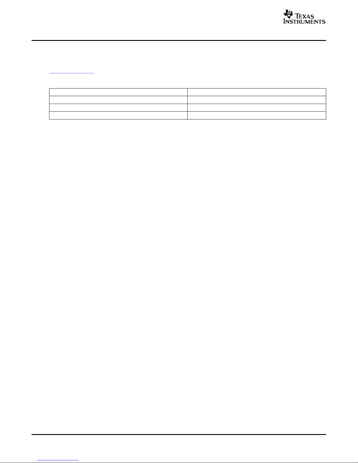
1 Related Documentation from Texas Instruments ........................................................................ 6
2-1 Recommended Supply Voltages for DAC8DIT2 Board ............................................................... 15
3-1 J11 Pin Description ........................................................................................................ 18
3-2 J12 Pin Description ........................................................................................................ 19
3-3 J21 Pin Description ........................................................................................................ 20
3-4 J22 Pin Description ........................................................................................................ 21
3-5 J200 Pin Description (Similar for J201 to J203) ........................................................................ 21
3-6 J140 Pin Description ....................................................................................................... 22
3-7 AP PSIA Pin Description .................................................................................................. 23
3-8 J301 Pin Description ....................................................................................................... 24
3-9 J800 Pin Description ....................................................................................................... 24
3-10 J71 Pin Description ........................................................................................................ 25
3-11 J62 Pin Description ........................................................................................................ 26
4 List of Figures SLEU065A – SEPTEMBER 2005 – Revised NOVEMBER 2006
Submit Documentation Feedback
Page 5

CAUTION
This is an example of a caution statement.
A caution statement describes a situation that could potentially
damage your software or equipment.
WARNING
This is an example of a warning statement.
A warning statement describes a situation that could potentially
cause harm to you.
About This Manual
This manual describes the operation of the TAS3108EVM2 evaluation module from Texas Instruments.
How to Use this Manual
This document contains the following chapters:
Chapter 1 - Overview
Chapter 2 - Quick Setup Guide
Chapter 3 - System Interfaces
Information About Cautions and Warnings
This manual may contain cautions and warnings.
Preface
SLEU065A – SEPTEMBER 2005 – Revised NOVEMBER
2006
Read This First
The information in a caution or a warning is provided for your protection. Please read each caution and
warning carefully.
SLEU065A – SEPTEMBER 2005 – Revised NOVEMBER 2006 Read This First 5
Submit Documentation Feedback
Page 6
www.ti.com
Related Documentation from Texas Instruments
Related Documentation from Texas Instruments
The following table contains a list of data manuals that have detailed descriptions of the integrated circuits
used in the design of the TAS3108EVM2. The data manuals can be obtained at the URL
http://www.ti.com .
Additional Documentation
1. TAS3108EVM2 Application Report
2. Graphical Development tool (GDE) for TAS3108 (GDE version 1.11 or later)
3. General Application Notes
Trademarks
PurePath Digital is a trademark of Texas Instruments.
All other trademarks are the property of their respective owners.
Table 1. Related Documentation from Texas Instruments
PART NUMBER LITERATURE NUMBER
TAS3108 SLES152
TLV1117-33 SLVS561
TPS3825-33 SLVS165
6 Read This First SLEU065A – SEPTEMBER 2005 – Revised NOVEMBER 2006
Submit Documentation Feedback
Page 7

SLEU065A – SEPTEMBER 2005 – Revised NOVEMBER
Overview
The TAS3108EVM2 PurePath Digital™ customer evaluation amplifier module
demonstrates the digital audio processor TAS3108/TAS3108IA from Texas Instruments
(TI).
TAS3108DCP/TAS3108IADCP is a fully programmable high-performance audio
processor. It uses an efficient, custom, multi-instruction programming environment
optimized for digital audio processing algorithms. The TAS3108/TAS3108IA
architecture provides high-quality audio processing by using a 48-bit data path, 28-bit
filter coefficients, and a single-cycle 28 × 48-bit multiplier with a 76-bit accumulator. An
embedded 8051 microprocessor provides algorithm and data control for the
TAS3108/TAS3108IA. The TAS3108 is the commercial version, intended for home
audio and other commercial applications. The TAS3108IA is the automotive version
that is qualified for use in automotive applications. This EVM uses the TAS3108
version, and the active/passive parts used are not qualified for automotive use.
This EVM is delivered together with two boards: an input board with SPDIF, ACD, and
USB for PC control, and an output board with DACs and a SPDIF transmitter. This
system is a complete eight-channel digital audio processor system that includes digital
input/output (S/PDIF), analog inputs/outputs, interface to PC, and DAP features like
digital volume control, input and output mixers, auto mute, equalization, tone controls,
loudness, dynamic range compression, and surround effects.
The TAS3108 applications could be automotive sound systems, digital televisions,
home theater systems, mini-component audio systems, and pro-audio.
Replacing the DAC-DIT output board with one of the TI PurePath digital-amplifier EVMs
makes it possible to test the TAS3108 with a speaker connected directly. Examples of
EVMs that can be connected include, but are not limited to, TAS5508-5142K7EVM,
TAS5518-5152K8EVM, TAS5518-5182C8EVM2, and TAS5086-5186V6EVM. This
system is designed for home theater applications such as A/V receivers, DVD
mini-component systems, home theater in a box (HTIB), DVD receivers, or plasma
display panels (PDP).
Chapter 1
2006
Topic .................................................................................................. Page
1.1 TAS3108EVM2 System Features ................................................... 8
1.2 PCB Key Map ............................................................................. 9
1.3 Input Board .............................................................................. 10
1.4 Output Board ............................................................................ 11
SLEU065A – SEPTEMBER 2005 – Revised NOVEMBER 2006 Overview 7
Submit Documentation Feedback
Page 8
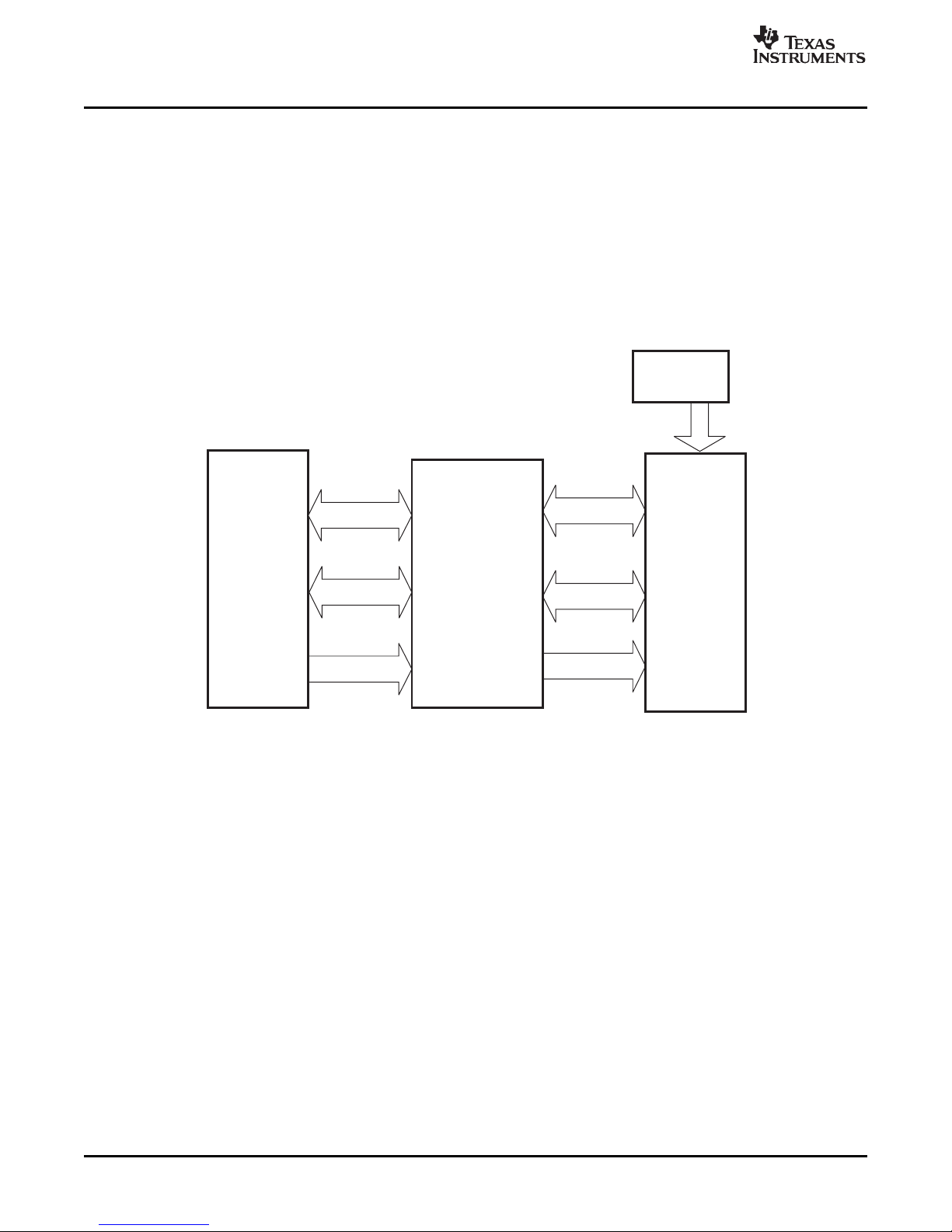
www.ti.com
8-Channel
Analog
Input
USB
Interface
Optical and
Coaxial
S/PDIF Input
Control Inferface
I2C Bus
I2S Bus
TAS3108EVM2
Module
TAS3108
EEPROM
Control Inferface
I2C Bus
I2S Bus
Power
Supplies
±15V
Power
Supplies
+5V
±12V
8-Channel
Analog
Output
Optical and
Coaxial
S/PDIF Ouput
Example
TI DAC-DIT Board
Example
TI Input-USB Board
TAS3108EVM2 System Features
1.1 TAS3108EVM2 System Features
• Socketed EEPROM for download of program and coefficients
• Eight-channel analog-to-digital converter, four PCM1802 devices, 102-dB DYR A-weighted
• Eight-channel digital-to-analog converter, two PCM4104 devices, 116-dB DYR A-weighted
• Two-channel SPDIF receiver, coaxial and optical input
• Two-channel SPDIF transmitter, coaxial and optical output
• I2S input and output connectors
• USB-to-PC connection for software control
• Double-sided plated-through PCB layout
Overview 8 SLEU065A – SEPTEMBER 2005 – Revised NOVEMBER 2006
Figure 1-1. TAS3108EVM2 System
Submit Documentation Feedback
Page 9
www.ti.com
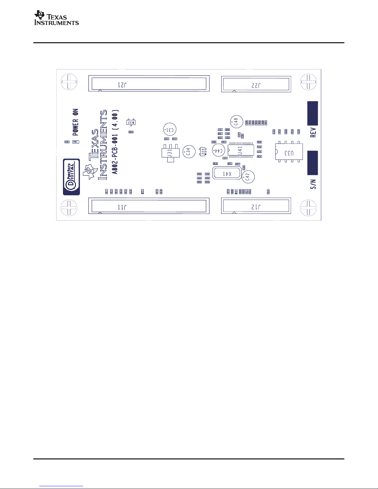
1.2 PCB Key Map
Physical structure for the TAS3108EVM2 is illustrated in Figure 1-2 .
PCB Key Map
Figure 1-2. Physical Structure for the TAS3108EVM2 (Rough Outline)
U41 is the TAS3108 device. U33 is the EEPROM for program and coefficient storage. Digital audio data
(I2S) is input on J12 and output on J22. J11 is used for I2C control, reset signal, and power-supply
voltage. Signals in J11 are duplicated in J21 for further control of a DAC output board or speaker amplifier.
D31, a green LED, indicates that the power-supply voltage is within specifications and that the device is
brought out of reset.
SLEU065A – SEPTEMBER 2005 – Revised NOVEMBER 2006 Overview 9
Submit Documentation Feedback
Page 10

www.ti.com
M UTE /UNM U TE
RESET button (board )
Input indicator
Digitalinputselect
ANALO G IN PUT - Ch 1 and 2
ANALO G IN PUT -Ch 3 and 4
ANALO G IN PUT - Ch 5 and 6
DIGITAL INPUT -O ptical
DIGITAL INPUT -Coaxial
ANALO G IN PUT - Ch 7 and 8
USB Connector
ANALO G Sam ple Rate
Input Indicator
DIGITAL INPUT - Optical
Digital Input Select
DIGITAL INPUT - Coaxial
ANALOG INPUT - Ch 3 and 4
ANALOG Sample Rate
ANALOG INPUT - Ch 5 and 6
ANALOG INPUT - Ch 7 and 8
USB Connector
RESET Button (Board)
ANALOG INPUT - Ch 1 and 2
MUTE / UNMUTE
Input Board
1.3 Input Board
The input board contains an eight-channel ADC, SPDIF receiver, and USB connection. Buttons for MUTE,
RESET, and selection between 48-kHz and 96-kHz sample rate.
Physical structure for the input-USB board is illustrated in Figure 1-3 .
Figure 1-3. Input Board Outline
Overview 10 SLEU065A – SEPTEMBER 2005 – Revised NOVEMBER 2006
Submit Documentation Feedback
Page 11

www.ti.com
1.4 Output Board
SPDIFDATA OUT select
SPDIFOutput-Coaxial
SPDIFOutput-Optical
ANALOGOUTPUT -Ch7and8
ANALOGOUTPUT -Ch5and6
ANALOGOUTPUT -Ch3and4
+/-15VPowerSupplyConnector
ANALOGOUTPUT -Ch1and2
SDIN1 SDIN2 SDIN3 SDIN4
U301
U301
U301
U301
Output Board
• Eight-channel digital-to-analog converter, two PCM4104 devices, automatic sample-rate detection, and
supports 44.1 kHz, 48 kHz, and 96 kHz in this application. Relation between master clock and sample
rate clock must be 256. 4-Vrms for 0-dB and 116-dB DYR A-weighted.
• Two-channel digital audio output, SPDIF format, DIT4192, optical and electrical output
• ± 12-V and 5-V power-supply regulators
The physical structure of the output DAC8-DIT2 board is illustrated in Figure 1-4 .
Figure 1-4. Physical Structure for Output DAC8-DIT2 Board Outline
SLEU065A – SEPTEMBER 2005 – Revised NOVEMBER 2006 Overview 11
Submit Documentation Feedback
Page 12

www.ti.com
Output Board
A picture of the complete system is shown in Figure 1-5 . The input board is to the left, the TAS3108EVM2
is in the middle, and the output board is to the right.
Figure 1-5. Complete System
12 Overview SLEU065A – SEPTEMBER 2005 – Revised NOVEMBER 2006
Submit Documentation Feedback
Page 13

SLEU065A – SEPTEMBER 2005 – Revised NOVEMBER
Quick Setup Guide
This chapter describes the TAS3108EVM2 board, with regard to power supplies and
system interfaces. The chapter provides information regarding handling and unpacking,
absolute operating conditions, and a description of the factory default switch and
jumper configuration.
This chapter provides a step-by-step guide to configuring the TAS3108EVM2 for device
evaluation.
Topic .................................................................................................. Page
2.1 Electrostatic Discharge Warning ................................................. 14
2.2 Unpacking the EVM ................................................................... 14
2.3 Power Supply Setup .................................................................. 15
2.4 Digital Audio Inputs/Outputs ...................................................... 15
2.5 Master/Slave Mode .................................................................... 15
2.6 TAS3108 Software Installation .................................................... 16
Chapter 2
2006
SLEU065A – SEPTEMBER 2005 – Revised NOVEMBER 2006 Quick Setup Guide 13
Submit Documentation Feedback
Page 14

www.ti.com
CAUTION
Failure to observe ESD handling procedues may result in damage
to EVM components.
Electrostatic Discharge Warning
2.1 Electrostatic Discharge Warning
Many of the components on the TAS3108EVM2 are susceptible to damage by electrostatic discharge
(ESD). Customers are advised to observe proper ESD handling precautions when unpacking and handling
the EVM, including the use of a grounded wrist strap at an approved ESD workstation.
2.2 Unpacking the EVM
Upon opening the TAS3108EVM2 package, please ensure that the following items are included:
• One TAS3108EVM2 board using one TAS3108DCP
• One TI input-USB board for interfacing TAS3108EVM2 with SPDIF receiver and eight-channel
analog-to-digital converter and USB for PC control
• One TI DAC8-DIT2 board for interfacing TAS3108EVM2 with SPDIF transmitter and digital-to-analog
converter outputs and power-supply regulators
• Two signal interface IDC cables for connection to an I2S back-end like the attached TI DAC8-DIT2
board, 14 pin
• Two control interface IDC cables for connection to an I2C back-end like the attached TI DAC8-DIT2
board, 34 pin
• One cable for connecting input-USB board to a USB port on a PC for TAS3108 control by software
• One cable for connecting DAC8-DIT2 board to the power supplies
• One PurePath CD-ROM containing data sheets, application notes, user's guides, gerber files, and PC
software tools
If any of these items are missing, please contact the Texas Instruments Product Information Center
nearest you to obtain a replacement.
Connect the input-USB board to TAS3108EVM2 using the two included delivered IDC cables. Connect
TAS3108EVM2 board to DAC8-DIT2 board using the two included IDC cables.
Quick Setup Guide14 SLEU065A – SEPTEMBER 2005 – Revised NOVEMBER 2006
Submit Documentation Feedback
Page 15

www.ti.com
2.3 Power Supply Setup
CAUTION
Applying voltages above the limitations given in the table above
may cause permanent damage to your hardware.
The TAS3108EVM2 is powered via the DAC8-DIT2 board or another output board, like a
TAS5086-5186EVM. The DAC8-DIT2 board generates a +5-V supply that is fed to the TAS3108EVM2.
The +5-V supply is further regulated to +3.3 V with the aid of a low-dropout linear regulator, U31.
Set the power supplies to ± 15 V, switch off the power supply, connect all cables to the EVM, and switch
on the power supply. Current consumption should be less than is shown in Table 2-1 . If it is higher, switch
off the power supply and double check the cabling.
DESCRIPTION VOLTAGE LIMITATIONS CURRENT REQUIREMENT CABLE
Power Supply Setup
Table 2-1. Recommended Supply Voltages for DAC8DIT2 Board
+15 V +14.5 V to +15.5 V 0.3 A J31 pin 2
–15 V –15.5 V to –14.4V 0.1 A J31 pin 1
2.4 Digital Audio Inputs/Outputs
The digital audio inputs can be connected to the board in two ways, either in the SPDIF format on the
coaxial connector or optical TosLink input or in I2S format on connector J12. The pinouts are shown in
Section 3.5 and Section 3.6 .
The digital audio outputs can be both SPDIF and I2S. SPDIF format is output on the coaxial connector
(J62) or optical TosLink® connector (J61), or I2S format is output on connector J22. Jumpers J301 and
J302 select the SDATA line to feed to the SPDIF transmitter.
2.5 Master/Slave Mode
The TAS3108EVM2 is delivered in Slave mode.
The SPDIF receiver, on the input board, is the MCLK clock master in this system.
The digital audio outputs can be both SPDIF and I2S. SPDIF format is output on coaxial connector, J62,
or optical TosLink, J61, or in I2S format on connector J22. Jumpers J301 and J302 selects the SDATA
line to feed to the SPDIF transmitter.
After each reset, either auto-generated during power-up sequence or manual pressing RESET button, the
input-USB board is always in the following configuration:
• Mute enabled
• Analog input set to 48-kHz sample rate
SLEU065A – SEPTEMBER 2005 – Revised NOVEMBER 2006 Quick Setup Guide 15
Submit Documentation Feedback
Page 16

www.ti.com
TAS3108 Software Installation
To start up a PurePath EVM, use following procedure:
1. Turn on all power supplies before connecting USB interface.
2. Connect USB interface and press RESET button.
3. Start GUI software and press RESET in GUI window. Make sure that the "USB attached" LED is on
and that the status indicator changes to "OK".
4. Load EVM configuration file. Ensure that the correct file is selected, according to the EVM in use.
5. Press MUTE to unmute the EVM.
6. The EVM is now ready to use.
2.6 TAS3108 Software Installation
The TAS3108 GDE and IDE software provide easy programming of the TAS3108 and enable
programming of the EEPROM on the EVM board.
1. Insert the PurePath CD-ROM
• If it does not autorun, run the ReadMe file.
• Select "SOFTWARE" in the menu to the left.
• Select the TAS3108 tools, and follow the instructions given to install.
2. After installation, turn on power supplies and connect USB cable to input-USB board.
3. Start GDE program from the Windows Start menu. Startup of GDE requires a few seconds.
To test the connection from PC to EVM, load the TAS3108EVM2 test file (helloworld.pfw), located in
C:\Program Files\Texas Instruments Inc\TAS3108 Development Tools\Examples\HelloWorld.pfw.
For more advanced use of the GDE, see the GDE online help, GDE release notes, and TAS3108 MCU
programmer's reference guide.
16 Quick Setup Guide SLEU065A – SEPTEMBER 2005 – Revised NOVEMBER 2006
Figure 2-1. TAS3108 GDE Window
Submit Documentation Feedback
Page 17

SLEU065A – SEPTEMBER 2005 – Revised NOVEMBER
System Interfaces
This chapter describes the TAS3108EVM2 board regard to power supplies and system
interfaces.
Topic .................................................................................................. Page
3.1 Control Interface (J11), Input ...................................................... 18
3.2 Digital Audio Interface, Input (J12) .............................................. 19
3.3 Control Interface, Output (J21) .................................................... 20
3.4 Digital Audio Interface, output (J22) ............................................ 21
3.5 Connectors on the Input-USB board ............................................ 21
3.6 Connectors on the DAC8-DIT2 Board .......................................... 25
Chapter 3
2006
SLEU065A – SEPTEMBER 2005 – Revised NOVEMBER 2006 System Interfaces 17
Submit Documentation Feedback
Page 18

www.ti.com
Control Interface (J11), Input
3.1 Control Interface (J11), Input
This interface connects the TAS3108EVM2 board to a TI input-USB board. This is a general-purpose
interface, so not all signals are used by the TAS3108. Unused signals are shaded in Table 3-1 .
PIN NO. DESCRIPTION
1 GND Ground
2 RESERVED
3 GND Ground
4 RESET System reset (bidirectional). Activate MUTE before RESET for quiet reset.
5 RESERVED
6 MUTE Ramp volume from any setting to noiseless soft mute. Mute can also be activated by I2C.
7 PDN Power down. TAS3108 goes ino power down state when activated.
8 RESERVED
9 RESERVED
10 SDA I2C data clock
11 GND Ground
12 SCL I2C bit clock
13 GPIO1
14 GPIO2
15 GPIO3
16 GPIO4 General-purpose input/output 4, used to reset the TAS3108 after programming.
17 GND Ground
18 GPIO5
19 GPIO6
20 SD Shutdown reporting. Used for speaker-output EVMs.
21 RESERVED
22 OTW Temperature warning. Used for speaker-output EVMs.
23 RESERVED
24 RESERVED
25 GND Ground
26 GND Ground
27 RESERVED
28 RESERVED
29 RESERVED
30 RESERVED
31 GND Ground
32 GND Ground
33 +5V +5-Vdc power supply (output)
34 +5V +5-Vdc power supply (output)
NET-NAME AT
SCHEMATICS
Table 3-1. J11 Pin Description
System Interfaces18 SLEU065A – SEPTEMBER 2005 – Revised NOVEMBER 2006
Submit Documentation Feedback
Page 19

www.ti.com
3.2 Digital Audio Interface, Input (J12)
The digital audio interface contains digital audio signal data (I2S), clocks, etc. See the TAS3108 data
manual for signal timing and details not covered in this document.
PIN NET-NAME AT DESCRIPTION
NUMBER SCHEMATICS
1 GND Ground
2 MCLK Master clock input
3 GND Ground
4 SDIN1 I2S data 1, Channel 1 and 2
5 SDIN2 I2S data 2, Channel 3 and 4
6 SDIN3 I2S data 3, Channel 5 and 6
7 SDIN4 I2S data 4, Channel 7 and 8
8 Reserved
9 Reserved
10 GND Ground
11 SCLK I2S bit clock
12 GND Ground
13 LRCLK I2S left-right clock
14 GND Ground
15 Reserved
16 GND Ground
Digital Audio Interface, Input (J12)
Table 3-2. J12 Pin Description
SLEU065A – SEPTEMBER 2005 – Revised NOVEMBER 2006 System Interfaces 19
Submit Documentation Feedback
Page 20

www.ti.com
Control Interface, Output (J21)
3.3 Control Interface, Output (J21)
This interface connects the TAS3108EVM2 board to a TI DAC8-DIT2 output board or a general amplifier
power EVM. This is a general-purpose interface, so not all signals are used by the TAS3108. Unused
signals are shaded in Table 3-3 .
PIN NO. DESCRIPTION
1 GND Ground
2 RESERVED
3 GND Ground
4 RESET System reset (bidirectional). Activate MUTE before RESET for quiet reset.
5 RESERVED
6 MUTE Ramp volume from any setting to noiseless soft mute. Mute can also be activated by I2C.
7 PDN Power down. TAS3108 goes ino power down state when activated.
8 RESERVED
9 RESERVED
10 SDA I2C data clock
11 GND Ground
12 SCL I2C bit clock
13 GPIO1
14 GPIO2
15 GPIO3
16 GPIO4 General-purpose input/output 4, used to reset the TAS3108 after programming.
17 GND Ground
18 GPIO5
19 GPIO6
20 SD Shutdown reporting. Used for speaker output EVMs.
21 RESERVED
22 OTW Temperature warning. Used for speaker output EVMs.
23 RESERVED
24 RESERVED
25 GND Ground
26 GND Ground
27 RESERVED
28 RESERVED
29 RESERVED
30 RESERVED
31 GND Ground
32 GND Ground
33 +5V +5-Vdc power supply (output)
34 +5V +5-Vdc power supply (output)
NET-NAME AT
SCHEMATICS
Table 3-3. J21 Pin Description
System Interfaces20 SLEU065A – SEPTEMBER 2005 – Revised NOVEMBER 2006
Submit Documentation Feedback
Page 21

www.ti.com
3.4 Digital Audio Interface, output (J22)
1
4
2 3
PCB Connector (TopView)
The digital audio interface contains digital audio signal data (I2S), clocks, etc. See the TAS3108 data
manual for signal timing and details not covered in this document.
PIN NO. NET-NAME AT DESCRIPTION
SCHEMATICS
1 GND Ground
2 MCLKO Master clock output
3 GND Ground
4 SDOUT1 I2S data 1, channels 1 and 2
5 SDOUT2 I2S data 2, channels 3 and 4
6 SDOUT3 I2S data 3, channels 5 and 6
7 SDOUT4 I2S data 4, channels 7 and 8
8 Reserved
9 Reserved
10 GND Ground
11 SCLKOUT I2S bit clock output
12 GND Ground
13 LRCLKO I2S left-right clock output
14 GND Ground
15 Reserved
16 GND Ground
Digital Audio Interface, output (J22)
Table 3-4. J22 Pin Description
3.5 Connectors on the Input-USB board
3.5.1 Analog Inputs
The mini-jack 3.5-mm connector for analog inputs is shown in Figure 3-1 .
Table 3-5. J200 Pin Description (Similar for J201 to J203)
PIN NO. NET-NAME AT DESCRIPTION
SCHEMATICS
1 CH1 Channel 1 input – tip
2 AGND Analog ground – sleeve
3 For future use
4 CH2 Channel 2 input – ring
Figure 3-1. J200 … J203 Pin Pumbers
SLEU065A – SEPTEMBER 2005 – Revised NOVEMBER 2006 System Interfaces 21
Submit Documentation Feedback
Page 22

www.ti.com
PCB Connector (TopView)
1 3
2
4
Connectors on the Input-USB board
3.5.2 SPDIF Coax
The SPDIF input for coax is shown in Figure 3-2 .
PIN NO. NET-NAME AT DESCRIPTION
1 GND Ground
2 IN1 Coax SPDIF input
3 IN1 Coax SPDIF input
4 IN1 Coax SPDIF input
Figure 3-2. J140 Pin Numbers
Table 3-6. J140 Pin Description
SCHEMATICS
3.5.3 AP PSIA Interface
The input-USB board provides the ability to input I2S directly into the PurePath EVM. I2S source could be,
for example, an Audio Precision with a Programmable Serial Interface Adaptor (PSIA).
Default jumper settings are shown in Figure 3-3 . In this setting, data out is: analog channels 1 and 2
routed to Data1, analog channels 3 and 4 to Data2, etc., when analog inputs are selected. When digital
input is selected, either coax or TosLink channel A+B is copied into all data outputs.
Figure 3-3. AP PSIA Default Setting
When using the input-USB board with an external I2S source connection, the jumper settings in Figure 3-4
should be used. Placing the jumper as shown copies I2S data into all data outputs.
22 System Interfaces SLEU065A – SEPTEMBER 2005 – Revised NOVEMBER 2006
Submit Documentation Feedback
Page 23

www.ti.com
GND
MCLK
SCLK
LRCLK
DATA
3
2
1
MCLK
SCLK
LRCLK
SDATA1
SDATA2
SDATA3
SDATA4
Figure 3-4. AP PSIA Settings Using External I2S Source
Connectors on the Input-USB board
Figure 3-5. AP PSIA Interface Pin Numbers
Table 3-7. AP PSIA Pin Description
PIN NO.
MCLK 1 MCLK Source From MCLK source
2 MCLK Out MCLK output
3 GND Ground
SCLK 1 SCLK Source From SCLK source
2 SCLK Out SCLK ouput
3 GND Ground
LRCLK 1 LRCLK Source From LRCLK source
2 LRCLK Out LRCLK output
3 GND Ground
SDATA1 1 SDATA1 Source From SPDIF or analog channels 1 and 2
2 SDATA1 Out SDATA1 output
3 GND Ground
SDATA2 1 SDATA2 Source From SPDIF or analog channels 3 and 4
2 SDATA2 Out SDATA2 output
3 SDATA1 Out Connected to SDATA1 Out
SDATA3 1 SDATA3 Source From SPDIF or analog channels 5 and 6
2 SDATA3 Out SDATA3 output
3 SDATA1 Out Connected to SDATA1 Out
NET-NAME AT DESCRIPTION
SCHEMATICS
SLEU065A – SEPTEMBER 2005 – Revised NOVEMBER 2006 System Interfaces 23
Submit Documentation Feedback
Page 24

www.ti.com
PCB Connector (TopView)
1
2
3
Connectors on the Input-USB board
PIN NO.
SDATA4 1 SDATA4 Source From SPDIF or analog channels 7 and 8
2 SDATA4 Out SDATA4 output
3 SDATA1 Out Connected to SDATA1 Out
3.5.4 I2C Connector (J301)
PIN NO. NET-NAME AT DESCRIPTION
1 SCL I2C clock
2 SDA I2C data
3 GND Ground
Table 3-7. AP PSIA Pin Description (continued)
NET-NAME AT DESCRIPTION
SCHEMATICS
Figure 3-6. J301 Pin Numbers
Table 3-8. J301 Pin Description
SCHEMATICS
3.5.5 Control Interface (J800)
This interface connects the EVM.
PIN NO. NET-NAME AT DESCRIPTION
1 GND Ground
2 RESERVED
3 GND Ground
4 RESET System reset (bidirectional). Activate MUTE before RESET for quiet reset.
5 RESERVED
6 MUTE Activate MUTE pin on modulator
7 RESERVED
8 RESERVED
9 RESERVED
10 SDA I2C data clock
11 GND Ground
12 SCL I2C bit clock
13 GPIO1 General-purpose port for GUIs
14 GPIO2 General-purpose port for GUIs
15 GPIO3 General-purpose port for GUIs
16 GPIO4 General-purpose port for GUIs
17 GND Ground
18 GPIO5 General-purpose port for GUIs
Table 3-9. J800 Pin Description
SCHEMATICS
24 System Interfaces SLEU065A – SEPTEMBER 2005 – Revised NOVEMBER 2006
Submit Documentation Feedback
Page 25

www.ti.com
PCB Connector (TopView)
1
4
2 3
Table 3-9. J800 Pin Description (continued)
PIN NO. NET-NAME AT DESCRIPTION
SCHEMATICS
19 GPIO6 General-purpose port for GUIs
20 SD1 Shutdown reporting
21 SD2 Shutdown reporting
22 TW1 Temperature warning
23 TW2 Temperature warning
24 RESERVED
25 GND Ground
26 GND Ground
27 RESERVED
28 RESERVED
29 RESERVED
30 RESERVED
31 GND Ground
32 GND Ground
33 +5V +5-Vdc power supply (output)
34 +5V +5-Vdc power supply (output)
Connectors on the DAC8-DIT2 Board
3.6 Connectors on the DAC8-DIT2 Board
3.6.1 Analog Outputs
The mini-jack 3.5-mm connector for analog outputs is shown in Figure 3-7 .
PIN NO. NET-NAME AT DESCRIPTION
SCHEMATICS
1 CH1 Channel 1, left output – tip
2 AGND Analog ground – sleeve
3 For future use
4 CH2 Channel 2, right output – ring
Figure 3-7. J71 to J74 Pin Numbers
Table 3-10. J71 Pin Description
SLEU065A – SEPTEMBER 2005 – Revised NOVEMBER 2006 System Interfaces 25
Submit Documentation Feedback
Page 26

www.ti.com
PCB Connector (TopView)
1 3
2
4
Connectors on the DAC8-DIT2 Board
3.6.2 3.6.2 SPDIF Coax
The SPDIF input for coax is shown in Figure 3-8 .
PIN NO. NET-NAME AT DESCRIPTION
1 GND Ground
2 IN1 Coax SPDIF output
3 IN1 Coax SPDIF output
4 IN1 Coax SPDIF output
Figure 3-8. J62 Pin Numbers
Table 3-11. J62 Pin Description
SCHEMATICS
System Interfaces26 SLEU065A – SEPTEMBER 2005 – Revised NOVEMBER 2006
Submit Documentation Feedback
Page 27

EVALUATION BOARD/KIT IMPORTANT NOTICE
Texas Instruments (TI) provides the enclosed product(s) under the following conditions:
This evaluation kit being sold by TI is intended for use for ENGINEERING DEVELOPMENT OR EVALUATION PURPOSES ONLY
and is not considered by TI to be fit for commercial use. As such, the goods being provided may not be complete in terms of
required design-, marketing-, and/or manufacturing-related protective considerations, including product safety measures typically
found in the end product incorporating the goods. As a prototype, this product does not fall within the scope of the European Union
directive on electromagnetic compatibility and therefore may not meet the technical requirements of the directive.
Should this evaluation kit not meet the specifications indicated in the EVM User's Guide, the kit may be returned within 30 days
from the date of delivery for a full refund. THE FOREGOING WARRANTY IS THE EXCLUSIVE WARRANTY MADE BY SELLER
TO BUYER AND IS IN LIEU OF ALL OTHER WARRANTIES, EXPRESSED, IMPLIED, OR STATUTORY, INCLUDING ANY
WARRANTY OF MERCHANTABILITY OR FITNESS FOR ANY PARTICULAR PURPOSE.
The user assumes all responsibility and liability for proper and safe handling of the goods. Further, the user indemnifies TI from all
claims arising from the handling or use of the goods. Please be aware that the products received may not be regulatory compliant
or agency certified (FCC, UL, CE, etc.). Due to the open construction of the product, it is the user's responsibility to take any and all
appropriate precautions with regard to electrostatic discharge.
EXCEPT TO THE EXTENT OF THE INDEMNITY SET FORTH ABOVE, NEITHER PARTY SHALL BE LIABLE TO THE OTHER
FOR ANY INDIRECT, SPECIAL, INCIDENTAL, OR CONSEQUENTIAL DAMAGES.
TI currently deals with a variety of customers for products, and therefore our arrangement with the user is not exclusive.
TI assumes no liability for applications assistance, customer product design, software performance, or infringement of
patents or services described herein.
Please read the User's Guide and, specifically, the Warnings and Restrictions notice in the User's Guide prior to handling the
product. This notice contains important safety information about temperatures and voltages. For additional information on TI's
environmental and/or safety programs, please contact the TI application engineer or visit www.ti.com/esh .
No license is granted under any patent right or other intellectual property right of TI covering or relating to any machine, process, or
combination in which such TI products or services might be or are used.
FCC Warning
This evaluation board/kit is intended for use for ENGINEERING DEVELOPMENT, DEMONSTRATION, OR EVALUATION
PURPOSES ONLY and is not considered by TI to be a finished end-product fit for general consumer use. It generates, uses, and
can radiate radio frequency energy and has not been tested for compliance with the limits of computing devices pursuant to part 15
of FCC rules, which are designed to provide reasonable protection against radio frequency interference. Operation of this
equipment in other environments may cause interference with radio communications, in which case the user at his own expense
will be required to take whatever measures may be required to correct this interference.
EVM WARNINGS AND RESTRICTIONS
It is important to operate this EVM within the range of 5-6V for the system supply.
Exceeding the specified input range may cause unexpected operation and/or irreversible damage to the EVM. If there are
questions concerning the input range, please contact a TI field representative prior to connecting the input power.
Applying loads outside of the specified output range may result in unintended operation and/or possible permanent damage to the
EVM. Please consult the EVM User's Guide prior to connecting any load to the EVM output. If there is uncertainty as to the load
specification, please contact a TI field representative.
During normal operation, some circuit components may have case temperatures greater than 75 ° C. The EVM is designed to
operate properly with certain components above 75 ° C as long as the input and output ranges are maintained. These components
include but are not limited to linear regulators, switching transistors, pass transistors, and current sense resistors. These types of
devices can be identified using the EVM schematic located in the EVM User's Guide. When placing measurement probes near
these devices during operation, please be aware that these devices may be very warm to the touch.
Mailing Address: Texas Instruments, Post Office Box 655303, Dallas, Texas 75265
Page 28

IMPORTANT NOTICE
Texas Instruments Incorporated and its subsidiaries (TI) reserve the right to make corrections, modifications, enhancements,
improvements, and other changes to its products and services at any time and to discontinue any product or service without notice.
Customers should obtain the latest relevant information before placing orders and should verify that such information is current and
complete. All products are sold subject to TI’s terms and conditions of sale supplied at the time of order acknowledgment.
TI warrants performance of its hardware products to the specifications applicable at the time of sale in accordance with TI’s
standard warranty. Testing and other quality control techniques are used to the extent TI deems necessary to support this
warranty. Except where mandated by government requirements, testing of all parameters of each product is not necessarily
performed.
TI assumes no liability for applications assistance or customer product design. Customers are responsible for their products and
applications using TI components. To minimize the risks associated with customer products and applications, customers should
provide adequate design and operating safeguards.
TI does not warrant or represent that any license, either express or implied, is granted under any TI patent right, copyright, mask
work right, or other TI intellectual property right relating to any combination, machine, or process in which TI products or services
are used. Information published by TI regarding third-party products or services does not constitute a license from TI to use such
products or services or a warranty or endorsement thereof. Use of such information may require a license from a third party under
the patents or other intellectual property of the third party, or a license from TI under the patents or other intellectual property of TI.
Reproduction of information in TI data books or data sheets is permissible only if reproduction is without alteration and is
accompanied by all associated warranties, conditions, limitations, and notices. Reproduction of this information with alteration is an
unfair and deceptive business practice. TI is not responsible or liable for such altered documentation.
Resale of TI products or services with statements different from or beyond the parameters stated by TI for that product or service
voids all express and any implied warranties for the associated TI product or service and is an unfair and deceptive business
practice. TI is not responsible or liable for any such statements.
TI products are not authorized for use in safety-critical applications (such as life support) where a failure of the TI product would
reasonably be expected to cause severe personal injury or death, unless officers of the parties have executed an agreement
specifically governing such use. Buyers represent that they have all necessary expertise in the safety and regulatory ramifications
of their applications, and acknowledge and agree that they are solely responsible for all legal, regulatory and safety-related
requirements concerning their products and any use of TI products in such safety-critical applications, notwithstanding any
applications-related information or support that may be provided by TI. Further, Buyers must fully indemnify TI and its
representatives against any damages arising out of the use of TI products in such safety-critical applications.
TI products are neither designed nor intended for use in military/aerospace applications or environments unless the TI products are
specifically designated by TI as military-grade or "enhanced plastic." Only products designated by TI as military-grade meet military
specifications. Buyers acknowledge and agree that any such use of TI products which TI has not designated as military-grade is
solely at the Buyer's risk, and that they are solely responsible for compliance with all legal and regulatory requirements in
connection with such use.
TI products are neither designed nor intended for use in automotive applications or environments unless the specific TI products
are designated by TI as compliant with ISO/TS 16949 requirements. Buyers acknowledge and agree that, if they use any
non-designated products in automotive applications, TI will not be responsible for any failure to meet such requirements.
Following are URLs where you can obtain information on other Texas Instruments products and application solutions:
Products Applications
Amplifiers amplifier.ti.com Audio www.ti.com/audio
Data Converters dataconverter.ti.com Automotive www.ti.com/automotive
DSP dsp.ti.com Broadband www.ti.com/broadband
Interface interface.ti.com Digital Control www.ti.com/digitalcontrol
Logic logic.ti.com Military www.ti.com/military
Power Mgmt power.ti.com Optical Networking www.ti.com/opticalnetwork
Microcontrollers microcontroller.ti.com Security www.ti.com/security
RFID www.ti-rfid.com Telephony www.ti.com/telephony
Low Power www.ti.com/lpw Video & Imaging www.ti.com/video
Wireless
Mailing Address: Texas Instruments, Post Office Box 655303, Dallas, Texas 75265
Wireless www.ti.com/wireless
Copyright © 2007, Texas Instruments Incorporated
Page 29

Mouser Electronics
Authorized Distributor
Click to View Pricing, Inventory, Delivery & Lifecycle Information:
Texas Instruments:
TAS3108EVM2
 Loading...