

Page 1

l
查询TAS3103供应商
Data M anua
February 2004 Digital Audio Solutions
SLES038C
Page 2

IMPORTANT NOTICE
Texas Instruments Incorporated and its subsidiaries (TI) reserve the right to make corrections, modifications,
enhancements, improvements, and other changes to its products and services at any time and to discontinue
any product or service without notice. Customers should obtain the latest relevant information before placing
orders and should verify that such information is current and complete. All products are sold subject to TI’s terms
and conditions of sale supplied at the time of order acknowledgment.
TI warrants performance of its hardware products to the specifications applicable at the time of sale in
accordance with TI’s standard warranty. Testing and other quality control techniques are used to the extent TI
deems necessary to support this warranty . Except where mandated by government requirements, testing of all
parameters of each product is not necessarily performed.
TI assumes no liability for applications assistance or customer product design. Customers are responsible for
their products and applications using TI components. To minimize the risks associated with customer products
and applications, customers should provide adequate design and operating safeguards.
TI does not warrant or represent that any license, either express or implied, is granted under any TI patent right,
copyright, mask work right, or other TI intellectual property right relating to any combination, machine, or process
in which TI products or services are used. Information published by TI regarding third-party products or services
does not constitute a license from TI to use such products or services or a warranty or endorsement thereof.
Use of such information may require a license from a third party under the patents or other intellectual property
of the third party, or a license from TI under the patents or other intellectual property of TI.
Reproduction of information in TI data books or data sheets is permissible only if reproduction is without
alteration and is accompanied by all associated warranties, conditions, limitations, and notices. Reproduction
of this information with alteration is an unfair and deceptive business practice. TI is not responsible or liable for
such altered documentation.
Resale of TI products or services with statements different from or beyond the parameters stated by TI for that
product or service voids all express and any implied warranties for the associated TI product or service and
is an unfair and deceptive business practice. TI is not responsible or liable for any such statements.
Following are URLs where you can obtain information on other Texas Instruments products and application
solutions:
Products Applications
Amplifiers amplifier.ti.com Audio www.ti.com/audio
Data Converters dataconverter.ti.com Automotive www.ti.com/automotive
DSP dsp.ti.com Broadband www.ti.com/broadband
Interface interface.ti.com Digital Control www.ti.com/digitalcontrol
Logic logic.ti.com Military www.ti.com/military
Power Mgmt power.ti.com Optical Networking www.ti.com/opticalnetwork
Microcontrollers microcontroller.ti.com Security www.ti.com/security
Telephony www.ti.com/telephony
Video & Imaging www.ti.com/video
Wireless www.ti.com/wireless
Mailing Address: Texas Instruments
Post Office Box 655303 Dallas, Texas 75265
Copyright 2004, Texas Instruments Incorporated
Page 3

Contents
Section Title Page
1 Introduction 1−1. . . . . . . . . . . . . . . . . . . . . . . . . . . . . . . . . . . . . . . . . . . . . . . . . . . . . . .
1.1 Features 1−1. . . . . . . . . . . . . . . . . . . . . . . . . . . . . . . . . . . . . . . . . . . . . . . . . . . .
1.2 Terminal Assignments 1−2. . . . . . . . . . . . . . . . . . . . . . . . . . . . . . . . . . . . . . . . .
1.3 Hardware Block Diagram 1−3. . . . . . . . . . . . . . . . . . . . . . . . . . . . . . . . . . . . . .
1.4 Functional Block Diagram 1−4. . . . . . . . . . . . . . . . . . . . . . . . . . . . . . . . . . . . .
1.5 Ordering Information 1−5. . . . . . . . . . . . . . . . . . . . . . . . . . . . . . . . . . . . . . . . . .
1.6 Terminal Functions 1−5. . . . . . . . . . . . . . . . . . . . . . . . . . . . . . . . . . . . . . . . . . .
1.7 Operational Modes 1−8. . . . . . . . . . . . . . . . . . . . . . . . . . . . . . . . . . . . . . . . . . .
1.7.1 Terminal-Controlled Modes 1−9. . . . . . . . . . . . . . . . . . . . . . . . . . . .
2
1.7.2 I
2 Hardware Architecture 2−1. . . . . . . . . . . . . . . . . . . . . . . . . . . . . . . . . . . . . . . . . . . . .
2.1 Input and Output Serial Audio Ports (SAPs) 2−3. . . . . . . . . . . . . . . . . . . . . .
2.1.1 SAP Configuration Options 2−3. . . . . . . . . . . . . . . . . . . . . . . . . . . .
2.1.2 Processing Flow—SAP Input to SAP Output 2−10. . . . . . . . . . .
2.2 DPLL and Clock Management 2−14. . . . . . . . . . . . . . . . . . . . . . . . . . . . . . . .
2.3 Controller 2−16. . . . . . . . . . . . . . . . . . . . . . . . . . . . . . . . . . . . . . . . . . . . . . . . . . .
2.3.1 8051 Microprocessor 2−16. . . . . . . . . . . . . . . . . . . . . . . . . . . . . . . .
2.3.2 I
2.4 Digital Audio Processor (DAP) Arithmetic Unit 2−21. . . . . . . . . . . . . . . . . . .
2.5 Reset 2−23. . . . . . . . . . . . . . . . . . . . . . . . . . . . . . . . . . . . . . . . . . . . . . . . . . . . . .
2.6 Power Down 2−23. . . . . . . . . . . . . . . . . . . . . . . . . . . . . . . . . . . . . . . . . . . . . . . .
2.7 Watchdog Timer 2−24. . . . . . . . . . . . . . . . . . . . . . . . . . . . . . . . . . . . . . . . . . . . .
2.8 General-Purpose I/O (GPIO) Ports 2−24. . . . . . . . . . . . . . . . . . . . . . . . . . . . .
2.8.1 GPIO Functionality—I
2.8.2 GPIO Functionality—I
3 Firmware Architecture 3−1. . . . . . . . . . . . . . . . . . . . . . . . . . . . . . . . . . . . . . . . . . . . .
3.1 I2C Coefficient Number Formats 3−1. . . . . . . . . . . . . . . . . . . . . . . . . . . . . . . .
3.1.1 28-Bit 5.23 Number Format 3−1. . . . . . . . . . . . . . . . . . . . . . . . . . .
3.1.2 48-Bit 25.23 Number Format 3−2. . . . . . . . . . . . . . . . . . . . . . . . . .
3.2 Input Crossbar Mixers 3−4. . . . . . . . . . . . . . . . . . . . . . . . . . . . . . . . . . . . . . . . .
3.3 3D Effects Block 3−8. . . . . . . . . . . . . . . . . . . . . . . . . . . . . . . . . . . . . . . . . . . . . .
3.3.1 CH1/CH2 Effects Block 3−8. . . . . . . . . . . . . . . . . . . . . . . . . . . . . . .
3.3.2 CH3 Effects Block 3−8. . . . . . . . . . . . . . . . . . . . . . . . . . . . . . . . . . .
3.4 Biquad Filters 3−10. . . . . . . . . . . . . . . . . . . . . . . . . . . . . . . . . . . . . . . . . . . . . . .
3.5 Bass and Treble Processing 3−11. . . . . . . . . . . . . . . . . . . . . . . . . . . . . . . . . .
3.5.1 Treble and Bass Processing and Concurrent I
3.6 Soft Volume/Loudness Processing 3−17. . . . . . . . . . . . . . . . . . . . . . . . . . . . .
C Bus-Controlled Modes 1−10. . . . . . . . . . . . . . . . . . . . . . . . . . .
2
C Bus Controller 2−16. . . . . . . . . . . . . . . . . . . . . . . . . . . . . . . . . .
2
C Master Mode 2−25. . . . . . . . . . . . . . . .
2
C Slave Mode 2−26. . . . . . . . . . . . . . . . . .
2
C
Read Transactions 3−15. . . . . . . . . . . . . . . . . . . . . . . . . . . . . . . . . .
iii
Page 4

3.6.1 Soft Volume 3−17. . . . . . . . . . . . . . . . . . . . . . . . . . . . . . . . . . . . . . . .
3.6.2 Loudness Compensation 3−24. . . . . . . . . . . . . . . . . . . . . . . . . . . .
3.6.3 Time Alignment and Reverb Delay Processing 3−26. . . . . . . . . .
3.7 Dynamic Range Control (DRC) 3−29. . . . . . . . . . . . . . . . . . . . . . . . . . . . . . . .
3.7.1 DRC Implementation 3−31. . . . . . . . . . . . . . . . . . . . . . . . . . . . . . . .
3.7.2 Compression/Expansion Coefficient Computation
Engine Parameters 3−33. . . . . . . . . . . . . . . . . . . . . . . . . . . . . . . . .
3.7.3 DRC Compression/Expansion Implementation Examples 3−35
3.8 Spectrum Analyzer/VU Meter 3−45. . . . . . . . . . . . . . . . . . . . . . . . . . . . . . . . .
3.9 Dither 3−47. . . . . . . . . . . . . . . . . . . . . . . . . . . . . . . . . . . . . . . . . . . . . . . . . . . . . .
3.9.1 Dither Seeds 3−48. . . . . . . . . . . . . . . . . . . . . . . . . . . . . . . . . . . . . . .
3.9.2 Dither Mix Options 3−50. . . . . . . . . . . . . . . . . . . . . . . . . . . . . . . . . .
3.9.3 Dither Gain Mixers 3−50. . . . . . . . . . . . . . . . . . . . . . . . . . . . . . . . . .
3.9.4 Dither Statistics 3−51. . . . . . . . . . . . . . . . . . . . . . . . . . . . . . . . . . . . .
3.10 Output Crossbar Mixers 3−54. . . . . . . . . . . . . . . . . . . . . . . . . . . . . . . . . . . . . .
4 Electrical Specifications 4−1. . . . . . . . . . . . . . . . . . . . . . . . . . . . . . . . . . . . . . . . . . . .
4.1 Absolute Maximum Ratings Over Operating Temperature Ranges 4−1. .
4.2 Recommended Operating Conditions 4−1. . . . . . . . . . . . . . . . . . . . . . . . . . .
4.3 Electrical Characteristics Over Recommended Operating
Conditions 4−2. . . . . . . . . . . . . . . . . . . . . . . . . . . . . . . . . . . . . . . . . . . . . . . . . . .
4.4 TAS3100 Timing Characteristics 4−3. . . . . . . . . . . . . . . . . . . . . . . . . . . . . . . .
4.4.1 Master Clock Signals Over Recommended Operating
Conditions 4−3. . . . . . . . . . . . . . . . . . . . . . . . . . . . . . . . . . . . . . . . . .
4.4.2 Control Signals Over Recommended Operating Conditions
4.4.3 Serial Audio Port Slave Mode Signals Over Recommended
Operating Conditions ) 4−5. . . . . . . . . . . . . . . . . . . . . . . . . . . . . . .
4.4.4 Serial Audio Port Master Mode Signals Over Recommended
Operating Conditions 4−6. . . . . . . . . . . . . . . . . . . . . . . . . . . . . . . . .
2
4.4.5 I
C Slave Mode Interface Signals Over Recommended
Operating Conditions 4−7. . . . . . . . . . . . . . . . . . . . . . . . . . . . . . . .
2
A.1 I
C Subaddress Table A−1. . . . . . . . . . . . . . . . . . . . . . . . . . . . . . . . . . . . . . . . .
A.2 TAS3103 Firmware Block Diagram A−19. . . . . . . . . . . . . . . . . . . . . . . . . . . . .
4−4. . . . . . . . . . . . . . . . . . . . . . . . . . . . . . . . . . . . . . . . . . . . . . . . . . . .
iv
Page 5

List of Illustrations
Figure Title Page
2−1 TAS3103 Detailed Hardware Block Diagram 2−2. . . . . . . . . . . . . . . . . . . . . . . . . . .
2−2 Discrete Serial Data Formats 2−3. . . . . . . . . . . . . . . . . . . . . . . . . . . . . . . . . . . . . . . .
2−3 Four-Channel TDM Serial Data Formats 2−3. . . . . . . . . . . . . . . . . . . . . . . . . . . . . .
2−4 SAP Configuration Subaddress Fields 2−4. . . . . . . . . . . . . . . . . . . . . . . . . . . . . . . .
2−5 Recommended Procedure for Issuing SAP Configuration Updates 2−5. . . . . . .
2−6 Format Options: Input Serial Audio Port 2−7. . . . . . . . . . . . . . . . . . . . . . . . . . . . . . .
2−7 TDM Format Options: Output Serial Audio Port 2−8. . . . . . . . . . . . . . . . . . . . . . . .
2−8 Discrete Format Options: Output Serial Audio Port 2−9. . . . . . . . . . . . . . . . . . . . .
2−9 Word Size Settings 2−9. . . . . . . . . . . . . . . . . . . . . . . . . . . . . . . . . . . . . . . . . . . . . . . . .
2−10 8 CH TDM Format Using SAP Modes 0101 and 1000 2−10. . . . . . . . . . . . . . . .
2−11 6 CH Data, 8 CH Transfer TDM Format Using SAP Modes
0101 and 1000 2−10. . . . . . . . . . . . . . . . . . . . . . . . . . . . . . . . . . . . . . . . . . . . . . . . .
2−12 SAP Input-to-Output Latency 2−11. . . . . . . . . . . . . . . . . . . . . . . . . . . . . . . . . . . . . .
2−13 SAP Input-to-Output Latency for I
2−14 DPLL and Clock Management Block Diagram 2−15. . . . . . . . . . . . . . . . . . . . . . .
2−15 I
2−16 I
2
C Slave Mode Communication Protocol 2−17. . . . . . . . . . . . . . . . . . . . . . . . . . .
2
C Subaddress Access Protocol 2−18. . . . . . . . . . . . . . . . . . . . . . . . . . . . . . . . . .
2−17 Digital Audio Processor Arithmetic Unit Block Diagram 2−21. . . . . . . . . . . . . . . .
2−18 DAP Arithmetic Unit Data Word Structure 2−22. . . . . . . . . . . . . . . . . . . . . . . . . . .
2−19 DAP ALU Operation With Intermediate Overflow 2−22. . . . . . . . . . . . . . . . . . . . .
2−20 TAS3103 Reset Circuitry 2−23. . . . . . . . . . . . . . . . . . . . . . . . . . . . . . . . . . . . . . . . . .
2−21 GPIO Port Circuitry 2−25. . . . . . . . . . . . . . . . . . . . . . . . . . . . . . . . . . . . . . . . . . . . . .
2−22 Volume Adjustment Timing—Master I
3−1 5.23 Format 3−1. . . . . . . . . . . . . . . . . . . . . . . . . . . . . . . . . . . . . . . . . . . . . . . . . . . . . . .
3−2 Conversion Weighting Factors—5.23 Format to Floating Point 3−1. . . . . . . . . . .
3−3 Alignment of 5.23 Coefficient in 32-Bit I
3−4 25.23 Format 3−2. . . . . . . . . . . . . . . . . . . . . . . . . . . . . . . . . . . . . . . . . . . . . . . . . . . . . .
3−5 Alignment of 5.23 Coefficient in 32-Bit I2C Word 3−3. . . . . . . . . . . . . . . . . . . . . . .
3−6 Alignment of 25.23 Coefficient in Two 32-Bit I
3−7 Serial Input Port to Processing Node Topology 3−5. . . . . . . . . . . . . . . . . . . . . . . . .
3−8. Input Mixer and Effects Block Topology—Internal Processing
Nodes A, B, C, D, E, and F 3−6. . . . . . . . . . . . . . . . . . . . . . . . . . . . . . . . . . . . . . . .
3−9 Input Mixer Topology—Internal Processing Nodes G and H 3−7. . . . . . . . . . . . . .
2
S Format Conversions 2−12. . . . . . . . . . . . .
2
C Mode 2−27. . . . . . . . . . . . . . . . . . . . . . .
2
C Word 3−2. . . . . . . . . . . . . . . . . . . . . . .
2
C Words 3−3. . . . . . . . . . . . . . . . .
v
Page 6

3−10 TAS3103 3D Effects Processing Block 3−9. . . . . . . . . . . . . . . . . . . . . . . . . . . . . . .
3−11 Biquad Filter Structure and Coefficient Subaddress Format 3−10. . . . . . . . . . . .
3−12 Bass and Treble Filter Selections 3−12. . . . . . . . . . . . . . . . . . . . . . . . . . . . . . . . . .
3−13 Bass and Treble Application Example—Subaddress Parameters 3−14. . . . . . .
3−14 I
2
C Bass/Treble Activity Monitor Procedure 3−16. . . . . . . . . . . . . . . . . . . . . . . . .
3−15 Soft Volume and Loudness Compensation Block Diagram 3−18. . . . . . . . . . . . .
3−16 Detailed Block Diagram—Soft Volume and Loudness Compensation 3−25. . .
3−17 Delay Line Memory Implementation 3−27. . . . . . . . . . . . . . . . . . . . . . . . . . . . . . . .
3−18 Maximum Delay Line Lengths 3−28. . . . . . . . . . . . . . . . . . . . . . . . . . . . . . . . . . . . .
3−19 DRC Positioning in TAS3103 Processing Flow 3−29. . . . . . . . . . . . . . . . . . . . . . .
3−20 Dynamic Range Compression (DRC) Transfer Function Structure 3−30. . . . . .
3−21 DRC Block Diagram 3−32. . . . . . . . . . . . . . . . . . . . . . . . . . . . . . . . . . . . . . . . . . . . . .
3−22 DRC Input Word Structure for 0-dB Channel Processing Gain 3−36. . . . . . . . .
3−23 DRC Transfer Curve—Example 1 3−38. . . . . . . . . . . . . . . . . . . . . . . . . . . . . . . . . .
3−24 DRC Transfer Curve—Example 2 3−40. . . . . . . . . . . . . . . . . . . . . . . . . . . . . . . . . .
3−25 DRC Transfer Curve—Example 3 3−42. . . . . . . . . . . . . . . . . . . . . . . . . . . . . . . . . .
3−26 DRC Transfer Curve—Example 4 3−44. . . . . . . . . . . . . . . . . . . . . . . . . . . . . . . . . .
3−27 Spectrum Analyzer/VU Meter Block Diagram 3−46. . . . . . . . . . . . . . . . . . . . . . . .
3−28 Logarithmic Number Conversions—Spectrum Analyzer/VU Meter 3−47. . . . . .
3−29 Dither Data Block Diagram 3−49. . . . . . . . . . . . . . . . . . . . . . . . . . . . . . . . . . . . . . . .
3−30 Dither Data Magnitude (Gain = 1.0) 3−51. . . . . . . . . . . . . . . . . . . . . . . . . . . . . . . .
3−31 Triangular Dither Statistics 3−52. . . . . . . . . . . . . . . . . . . . . . . . . . . . . . . . . . . . . . . .
3−32 Triangular Dither Statistics 3−53. . . . . . . . . . . . . . . . . . . . . . . . . . . . . . . . . . . . . . . .
3−33 Processing Node to Serial Output Port Topology 3−55. . . . . . . . . . . . . . . . . . . . .
3−34 Output Crossbar Mixer Topology 3−56. . . . . . . . . . . . . . . . . . . . . . . . . . . . . . . . . . .
4−1 Master Clock Signals Timing Waveforms 4−3. . . . . . . . . . . . . . . . . . . . . . . . . . . . . .
4−2 Control Signals Timing Waveforms 4−4. . . . . . . . . . . . . . . . . . . . . . . . . . . . . . . . . . .
4−3 Serial Audio Port Slave Mode Timing Waveforms 4−5. . . . . . . . . . . . . . . . . . . . . .
4−4 TAS3100 Serial Audio Port Master Mode Timing Waveforms 4−6. . . . . . . . . . . . .
2
4−5 I
4−6 I
C SCL and SDA Timing Waveforms 4−8. . . . . . . . . . . . . . . . . . . . . . . . . . . . . . . . .
2
C Start and Stop Conditions Timing Waveforms 4−8. . . . . . . . . . . . . . . . . . . . . .
vi
Page 7

List of Tables
Table Title Page
2−1 TAS3103 Throughput Latencies vs MCLK and LRCLK 2−13. . . . . . . . . . . . . . . . .
2−2 TAS3103 Clock Default Settings 2−16. . . . . . . . . . . . . . . . . . . . . . . . . . . . . . . . . . . .
2
2−3 I
2−4 Four Byte Write Exceptions—Reserved and Factory-Test I
2−5 Four Byte Read Exceptions—Reserved and Factory-Test I
2−6 GPIO Port Functionality—I
3−1 Biquad Filter Breakout 3−10. . . . . . . . . . . . . . . . . . . . . . . . . . . . . . . . . . . . . . . . . . . . .
3−2 Bass Shelf Filter Indices for 1/2-dB Adjustments 3−14. . . . . . . . . . . . . . . . . . . . . .
3−3 Treble Shelf Filter Indices for 1/2-dB Adjustments 3−15. . . . . . . . . . . . . . . . . . . . .
3−4 Volume Adjustment Gain Coefficients 3−20. . . . . . . . . . . . . . . . . . . . . . . . . . . . . . . .
3−5 DRC Example 2 Parameters 3−39. . . . . . . . . . . . . . . . . . . . . . . . . . . . . . . . . . . . . . .
3−6 DRC Example 3 Parameters 3−41. . . . . . . . . . . . . . . . . . . . . . . . . . . . . . . . . . . . . . .
3−7 DRC Example 4 Parameters 3−45. . . . . . . . . . . . . . . . . . . . . . . . . . . . . . . . . . . . . . .
3−8 Mixer Gain Setting for LSB Dither Data Insertion 3−50. . . . . . . . . . . . . . . . . . . . . .
C EEPROM Data 2−19. . . . . . . . . . . . . . . . . . . . . . . . . . . . . . . . . . . . . . . . . . . . . . . .
2
C
Subaddresses 2−20. . . . . . . . . . . . . . . . . . . . . . . . . . . . . . . . . . . . . . . . . . . . . . . . . .
2
C
Subaddresses 2−21. . . . . . . . . . . . . . . . . . . . . . . . . . . . . . . . . . . . . . . . . . . . . . . . . .
2
C Master Mode 2−25. . . . . . . . . . . . . . . . . . . . . . . . . .
vii
Page 8

viii
Page 9

1 Introduction
The TAS3103 is a fully configurable digital audio processor that preserves high-quality audio by using a 48-bit data
path, 28-bit filter coefficients, and a single cycle 28 x 48-bit multiplier and 76-bit accumulator. Because of the
coefficient-configurable fixed-program architecture of the TAS3103, a complete set of user-specific audio processing
functions can be realized, with short development times, in a small, low power , low-cost device. A personal computer
(PC) GUI-based software development package and a comprehensive evaluation board provide additional facilities
to further reduce development times. The TAS3103 uses 1.8-V core logic with 3.3-V I/O buffers, and requires only
3.3-V power. The TAS3103 is available in a 38-pin TSSOP package.
1.1 Features
• Audio Input/Output
− Four Serial Audio Input Channels
− Three Serial Audio Output Channels
− 8-kHz to 96-kHz Sample Rates Supported
− 15 Stereo/TDM Data Formats Supported
− Input/Output Data Format Selections Independent
− 16-, 18-, 20-, 24-, and 32-Bit Word Sizes Supported
2
• Serial Master/Slave I
• Three Independent Monaural Processing Channels
− Programmable Four Stereo Input Digital Mixer
− 3D Effect and Reverb Structure and Filters
− Programmable 12 Band Digital Parametric EQ
− Programmable Digital Bass and Treble Controls
− Programmable Digital Soft Volume Control (24 dB to −-∞ dB)
− Soft Mute/Unmute
− Programmable Dither
− Programmable Loudness Compensation
− VU Meter and Spectral Analysis I
− Programmable Channel Delay (Up to 42 ms at 48 kHz)
− 192-dB Dynamic Range (Supports Up to 32-Bit Audio Data)
− Dual Threshold Dynamic Range Compression/Expansion
C Control Channel
2
C Output
• Electrical and Physical
− Single 3.3-V Power Supply
− 38-Pin TSSOP Package
− Low Power Standby
1−1
Page 10
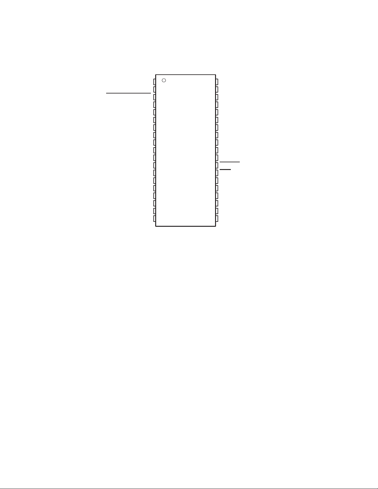
1.2 Terminal Assignments
DBT PACKAGE
(TOP VIEW)
SCLKIN
PWRDN
REGULATOR_EN
XT ALI (1.8-V logic)
XTALO (1.8-V logic)
AVDD_BYPASS_CAP
A_VDDS (3.3 V)
AVSS
MCLKI
TEST
MICROCLK_DIV
I2C_SDA
I2C_SCL
SDIN1
SDIN2
SDIN3
SDIN4
GPIO0
GPIO1
1
2
3
4
5
6
7
8
9
10
11
12
13
14
15
16
17
18
19
LRCLK
38
ORIN
37
SCLKOUT2
36
SCLKOUT1
35
MCLKO
34
SDOUT3
33
SDOUT2
32
VDDS (3.3 V)
31
SDOUT1
30
DVDD_BYPASS_CAP
29
DVSS
28
I2CM_S
27
RST
26
CS1
25
CS0
24
PLL1
23
PLL0
22
GPIO3
21
GPIO2
20
1−2
Page 11
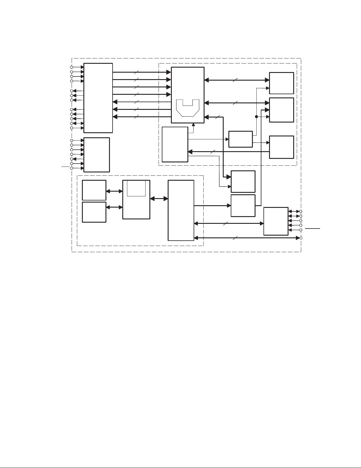
1.3 Hardware Block Diagram
SDIN1
SDIN2
SDIN3
SDIN4
SDOUT1
SDOUT2
SDOUT3
SCLKOUT2
SCLKOUT1
MCLKO
LRCLK
SCLKIN
TEST
PWRDN
PLL1
PLL0
XTALO
XTALI
RST
Serial
Audio
Port
Oscillator
and
PLL
External
Data
RAM
Code
ROM
64
64
64
64
64
64
64
Internal
Data
RAM
8051
MCU
(8-Bit)
Controller
Control
Registers
Data
Path
76-Bit
ALU
Digital Audio Processor
28
2828
48
48
Memory
Interface
54
Delay
Memory
(4K x 16)
Volume
Update
8
8
4
4
COEF
RAM
Data
RAM
Code
ROM
I2C
Serial
Interface
I2C_SDA
I2C_SCL
CS1
CS0
I2CM_S
GPIO[3:0]
1−3
Page 12
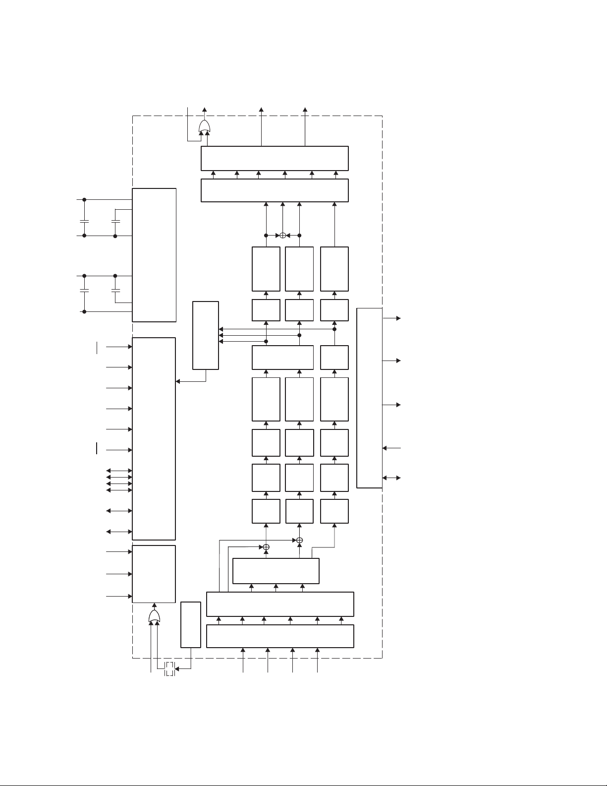
ORIN
SDOUT1
Multi-
SDOUT2
PCM
mode
Cross-
Output
to
bar
Serial
Output
Multi-
plexer
SDOUT3
Port
AVSS A_VDDS
VDDS DVSS
AVDD_
BYPASS_
DVDD_
BYPASS_
M_S
I2C_
Test PWRDN
RST
GPIO(3:0) CS0 CS1PLL1
CAP
CAP
Voltage Regulation
Microprocessor
or
VU Meter
Spectrum Analyzer
Ch2
Center
Ch1
DRC
Ganged
Dither
Programmable
Delay
Loudness
Compensation
Soft
Volume
and
Bass
Treble
Dither
Programmable
Delay
Loudness
Compensation
Soft
Volume
and
Bass
Treble
3 Mono Processing Channels
Ch3
Dither
Programmable
Delay
DRC
Loudness
Compensation
Soft
Volume
and
Bass
Treble
S Clock Input/Generation
2
I
LRCLK SCLKIN SCLKOUT1 SCLKOUT2 MCLKO
SCL
I2C_
SDA
I2C_
and
PLL
Dividers
PLL0 MC/Div
XTALI
MCLKI
1.4 Functional Block Diagram
1−4
Oscillator
XTALO
SDIN1
12
Ch1
Multi-
Multi-
Filters
Biquad
3D
Mode
Input
Cross-
Mode
Serial
SDIN2
bar
to
Effects
Mixer
PCM
12
Ch2
Block
Input
SDIN3
Filters
Biquad
Port
SDIN4
12
Ch3
Filters
Biquad
Ch3
Page 13
1.5 Ordering Information
PULLUP/
DESCRIPTION
PULLUP/
1.6 Terminal Functions
PLASTIC
T
A
0°C to 70°C TAS3103DBT
−40°C to 85°C TAS3103IDBT
38-PIN TSSOP
(DBT)
TERMINAL
NAME NO. I/O TYPE
A_VDDS (3.3 V) 7 PWR The PWR pin is used to input 3.3-V power to the DPLL and clock oscillator.
AVDD_BYPASS_CAP 6 PWR AVDD_BYPASS_CAP is a pinout of the internally regulated 1.8-VDC power
AVSS 8 PWR AVSS is the ground reference for the internal DPLL and oscillator circuitry.
CS0 24 I D CS0 is the LSB of a 2-bit code used to generate part of an I2C device address
CS1 25 I D CS1 is the MSB of a 2-bit code used to generate part of an I2C device address
DVDD_BYPASS_CAP 29 PWR DVDD_BYPASS_CAP is a pin-out of the internally regulated 1.8-V power
DVSS 28 PWR DVSS is the digital ground pin. None
GPIO0 18 I/O D GPIO0 is a general-purpose I/O, controlled by the internal microprocessor
GPIO1 19 I/O D GPIO1 is a general-purpose I/O, controlled by the internal microprocessor
GPIO2 20 I/O D GPIO2 is a general-purpose I/O, controlled by the internal microprocessor
GPIO3 21 I/O D GPIO3 is a general-purpose I/O, controlled by the internal microprocessor
I2CM_S 27 I D I2CM_S is a non-latched input that determines whether the TAS3103 acts as
(1)
This pin can be connected to the same power source used to drive the DVSS
power pin. To achieve low DPLL jitter, this pin should be bypassed to AVSS
with a 0.01-µF capacitor (low ESR preferable).
used by the DPLL and crystal oscillator . This pin should be connected to pin 8
with a 0.01-µF capacitor (low ESR preferable). This pin must not be used to
power external devices.
This pin needs to reference the same ground as DVSS power pin. To achieve
low DPLL jitter, ground noise at this pin must be minimized. The availability of
the AVSS pin allows a designer to use optimizing techniques such as star
ground connections, separate ground planes, or other quiet ground
distribution techniques to achieve a quiet ground reference at this pin.
that makes it possible to address four TAS3103 ICs on the same bus without
additional chip select logic. The pulldowns on the inputs select 00 as a default
when neither pin is connected.
that makes it possible to address four TAS3103 ICs on the same bus without
additional chip select logic.
used by all internal digital logic. This pin must not be used to power external
devices. A low ESR capacitor of at least 470 nF should be placed as close to
the device as possible between this pin and pin 28.
through I2C commands. When in the I2C master mode, GPIO0 serves as a
volume up command for CH1/CH2.
through I2C commands. When in the I2C master mode, GPIO1 serves as a
volume down command for CH1/CH2.
through I2C commands. When in the I2C master mode, GPIO2 serves as a
volume up command for CH3.
through I2C commands. When in the I2C master mode, GPIO3 serves as a
volume down command for CH3.
an I2C master or slave. Logic high, or no connection, sets the TAS3103 as an
I2C master device. A logic low sets the TAS3103 as an I2C slave device. As a
master I2C device, the TAS3103 I2C port must have access to an external
EEPROM for input.
DOWN
None
None
None
Pulldown
Pulldown
None
Pullup
Pullup
Pullup
Pullup
Pullup
(2)
1−5
Page 14

TERMINAL
(1)
TYPE
NAME
I2C_SCL 13 I/O D I2C_SCL is the I2C clock pin. When the TAS3103 I2C port is a master,
I/ONO.
I2C_SCL is (1/2N) x (1/(M+1)) x 1/10 times the microprocessor clock, where N
and M are set to 2 and 8 respectively. When the TAS3103 I2C port is a slave,
input clock rates up to 400 kHz can be supported. This pin must be provided an
external pullup (5 kΩ is recommended for most applications).
DESCRIPTION
DESCRIPTION
PULLUP/
PULLUP/
(2)
(2)
DOWN
DOWN
External
pullup
required
I2C_SDA 12 I/O D I2C_SDA is the I2C bidirectional data pin. The TAS3103 I2C port can support
data rates up to 400K bits/sec. This pin must be provided an external pullup
(5 kΩ is recommended for most applications).
LRCLK 38 I/O D LRCLK is either an input or an output, depending on whether the T AS3103 is in
a master or slave serial audio port mode, which is determined by bit 22 of
subaddress 0xF9.
MCLKI 9 I D MCLKI is a master clock input that provides an alternative to using a fixed
crystal frequency. In DPLL modes, the input frequency of this clock can range
from 2.8 MHz to 24.576 MHz. In PLL bypass mode, frequencies up to 136 MHz
can be used. Whenever MCLKI is not used and XTALI/XTALO provide the
master clock input, MCLKI must be grounded.
MCLKO 34 O D MCLKO is the master output clock pin. It is produced by dividing MCLKI/XTALI
by 1, 2, or 4 (depending on the setting of a subaddress control field). MCLKO is
provided to interconnect, without the need for additional glue logic, the
TAS3103 interfaces chips that require different multiples of the audio sample
rate (FS) as a master clock.
MICROCLK_DIV 11 I D MICROCLK_DIV sets the division ratio between the digital audio processing
clock and the internal microprocessor clock. The audio-processing clock is the
DPLL output clock if PLL_bypass is not enabled. The audio-processing clock
is MCLKI/XTALI master clock if PLL_bypass is enabled. Logic high on this pin
sets the microprocessor clock equal to the audio-processing clock. A logic low
sets the microprocessor clock to 1/4 the digital audio-processing clock.
MICROCLK_DIV must be set low if the audio processing clock is > 36 MHz.
MICROCLK_DIV must be set high if the audio processing clock is ≤ 36 MHz.
ORIN 37 I D ORIN allows the processing of a multichannel signal set through two
TAS3103s without any additional components. One use of ORIN would be to
fully emulate a 6-channel audio processor at speeds up to a 96-kHz sample
rate with only two TAS3103s and no glue logic.
The two-chip configuration is accomplished by wiring the SDOUT1 port of one
of the two TAS3103 chips to the ORIN port of the second T AS3103. Internal to
the chip, the ORIN input is OR’ed with internal SDOUT1 data to generate the
resulting output data on channel SDOUT1. For TDM output formats, the
SDOUT1 outputs of the two chips differ in phasing in both the left and right
channels to arrive at the proper composite output. For discrete outputs, one
chip contributes the left channel of the composite SDOUT1, and the other chip
contributes the right channel of the composite SDOUT1.
If not used, ORIN must be connected to ground.
External
pullup
required
Pulldown
None
None
Pulldown
Pulldown
PLL0 22 I D PLL0 is the LSB of a 2-bit code used to select four different modes of DPLL
multiplexer/input divider operation. PLL[1:0] values of 00, 01, and 10 select
the DPLL input clock to be MCLKI/XTALI divided by 1, 2, and 4 respectively. A
value of 11 results in MCLKI/XT ALI being substituted for the DPLL output. The
pullup/pulldown combination provides a default of 01 when neither pin is
connected.
PLL1 23 I D PLL1 is the MSB of a 2-bit code used to select four different modes of DPLL
multiplexer/input divider operation. PLL[1:0] values of 00, 01, and 10 select
the DPLL input clock to be MCLKI/XTALI divided by 1, 2, and 4 respectively. A
value of 11 results in MCLKI/XT ALI being substituted for the DPLL output. The
pullup/pulldown combination provides a default of 01 when neither pin is
connected.
1−6
Pullup
Pulldown
Page 15

TERMINAL
(1)
TYPE
NAME
PWRDN 2 I D PWRDN powers down all logic and stops all clocks whenever logic high is
REGULATOR_EN 3 I D REGULATOR_EN is only used in factory tests. This pin should always be tied
RST 26 I D RST is the master reset input. Applying a logic low to this pin generates a
SCLKIN 1 I D SCLKIN is the serial audio port (SAP) input data clock. This clock is only used
SCLKOUT1 35 O D SCLKOUT1 is one of two serial output bit clocks. It is divided from
SCLKOUT2 36 O D SCLKOUT2 is one of two serial output bit clocks. It is divided from
SDIN1 14 I D SDIN1, SDIN2, SDIN3, and SDIN4 are the four TAS3103 serial data input
SDIN2 15 I D SDIN2 is one of the four TAS3103 serial data input ports. SDIN2 supports four
SDIN3 16 I D SDIN3 is one of the four TAS3103 serial data input ports. SDIN4 supports four
SDIN4 17 I D SDIN4 is one of the four TAS3103 serial data input ports. SDIN4 supports four
SDOUT1 30 O D SDOUT1, SDOUT2, and SDOUT3 are the three TAS3103 serial data output
SDOUT2 32 O D SDOUT2 is one of the three serial data output ports. SDOUT2 supports four
SDOUT3 33 O D SDOUT3 is one of the three serial data output ports. SDOUT3 supports four
TEST 10 I D TEST is only used in factory tests. This pin must be left unconnected or
I/ONO.
applied. However, the coefficient memory remains stable through a power
down cycle, as long as a reset is not sent after a power down cycle.
to ground.
master reset. The master reset results in all coefficients being set to their
power-up default state, all data memories being cleared, and all logic signals
being returned to their default values.
when the SAP is a slave. In master mode, SCLKOUT1 internally provides the
serial input clock (SCLKOUT1 from a given TAS3103 must not be connected
to SCLKIN on the same TAS3103 chip).
MCLKI/XTALI in master mode, and SCLKIN in slave mode. Subaddress
control fields determine the divide ratio in both cases. When the serial audio
port is in a master mode, SCLKOUT1 is used to receive incoming serial data
and should be wired to the data source(s) providing data to the SDIN inputs.
MCLKI/XTALI in master mode, and SCLKIN in slave mode. Subaddress
control fields determine the divide ratio in both cases. SCLKOUT2 is always
used to clock out serial data from the three serial SDOUT output data
channels. SCLKOUT2 is provided separately from SCLKOUT1 to allow
discrete in to TDM out and TDM in to discrete out data format conversions
without the use of external glue logic.
ports. All four input ports support four discrete (stereo) data formats. SDIN1 is
the only data input port that also supports eleven time division multiplexed
data formats. All four ports are capable of receiving data with bit rates up to
24.576 MHz.
discrete (stereo) data formats, and is capable of receiving data with bit rates
up to 24.576 MHz.
discrete (stereo) data formats, and is capable of receiving data with bit rates
up to 24.576 MHz.
discrete (stereo) data formats, and is capable of receiving data with bit rates
up to 24.576 MHz.
ports. All three output ports support four discrete (stereo) data formats.
SDOUT1 is the only data output port that also supports eleven time division
multiplexed data formats. All three ports are capable of outputting data at bit
rates up to 24.576 MHz.
discrete (stereo) data formats, and is capable of outputting data at bit rates up
to 24.576 MHz.
discrete (stereo) data formats, and is capable of outputting data at bit rates up
to 24.576 MHz.
grounded.
DESCRIPTION
DESCRIPTION
PULLUP/
PULLUP/
DOWN
DOWN
Pulldown
None
Pullup
Pulldown
None
Output
Pulldown
Pulldown
Pulldown
Pulldown
None
None
None
Pulldown
(2)
(2)
1−7
Page 16
TERMINAL
(1)
TYPE
NAME
VDDS (3.3 V) 31 - PWR VDDS is the 3.3-V pin that powers (1) the 1.8-V internal power regulator used
XTALI (1.8-V logic) 4 I A XTALO and XTALI provide a master clock for the TAS3103 via use of an
XTALO (1.8-V logic) 5 O A XTALO and XTALI provide a master clock for the TAS3103 via use of an
NOTES: 1. TYPE: A = analog; D = 3.3-V digital; PWR = power/ground/decoupling
2. All pullups are 20-µA weak pullups and all pulldowns are 20-µA weak pulldowns. The pullups and pulldowns are included to assure
proper input logic levels if the pins are left unconnected (pullups => logic 1 input; pulldowns => logic 0 input). Devices that drive inputs
with pullups must be able to sink 20 µA while maintaining a logic 0 drive level. Devices that drive inputs with pulldowns must be able
to source 20 µA, while maintaining a logic 1 drive level.
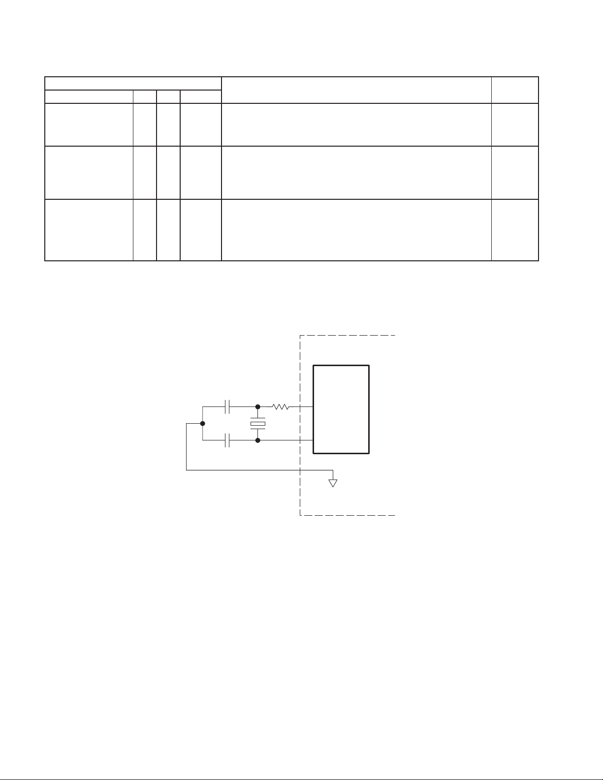
3. Crystal type and recommended circuit:
I/ONO.
to supply logic power to the chip and (2) the I/O ring. It is recommended that
this pin be bypassed to DVSS (pin 28) with a low ESR capacitor in the range of
0.01 µF.
external fundamental mode crystal. XTALI is the 1.8-V input port for the
oscillator circuit. See Note 3 for recommended crystal type and accompanying
circuitry. This pin should be grounded when the MCLKI pin is used as the
source for the master clock.
external fundamental mode crystal. XTALO is the 1.8-V output drive to the
crystal. XTALO can support crystal frequencies between 2.8 MHz and
20 MHz. See Note 3 for recommended crystal type and accompanying
circuitry. This pin should be left unconnected in applications using an external
clock input to MCLKI.
DESCRIPTION
DESCRIPTION
TAS3103
PULLUP/
PULLUP/
(2)
(2)
DOWN
DOWN
None
None
None
OSC
C
1
C
2
r
d
Circuit
XO
XI
AVSS
• Crystal type = parallel-mode, fundamental-mode crystal
= drive level control resistor—vendor specified
• r
d
• C
= Crystal load capacitance (capacitance of circuitry between the two terminals of the crystal)
L
• C
= (C1× C2) / (C1 + C2) + CS (where CS = board stray capacitance ~2 pF)
L
− Example: Vendor recommended C
= 18 pF, CS = 3 pF ⇒ C1 = C2 = 2 x (18 − 3) = 30 pF
L
1.7 Operational Modes
The TAS3103 operation is governed by I/O terminal voltage level settings and register / coefficient settings within the
TAS3103. The terminal settings are wholly sufficient to address all external environments - allowing the remaining
configuration settings to be determined by either I
2
the I
C master mode is selected).
2
C commands or by the content of an I2C serial EEPROM (when
1−8
Page 17
1.7.1 Terminal-Controlled Modes
ÎÎ
1.7.1.1 Clock Control
PLL1 PLL0 DAP CLOCK
0 0 11 x MCLK
0 1 (11 x MCLK)/2
1 0 (11 x MCLK)/4
1 1 MCLK (PLL bypass)
MICROCLK_DIV MICROPROCESSOR CLOCK
XTALIMCLKI
PLL0
0 DAP clock/4
1 DAP clock
PLL1
MICROCLK_DIV
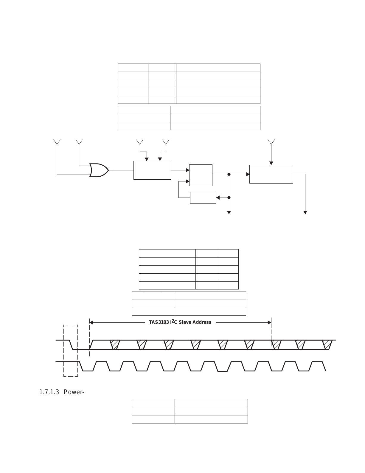
1.7.1.2 I2C Bus Setup
MCLK
Reference
Divider
PLL
÷ 11
Audio Processor
1400 x Fs 3 DAP Clock 3 136 MHz
SLAVE ADDRESS CS1 CS0
0x68/69 0 0
0x6A/6B 0 1
0x6C/D 1 0
0x6E/6F 1 1
I2CM_S I2C BUS MODE
0 Slave
1 Master
TAS3103 I2C Slave Address
Digital
(DAP) Clock
Microprocessor
Scaler
Microprocessor
Clock < 36 MHz
SDA
SCL
Start
a6 = 0 a5 = 1 a4 = 1 a3 = 0 a2 = 1 a1=CS1 a0=CS0 R/W ACK
123456789
1.7.1.3 Power-Down/Sleep Selection
PWRDN POWER STATUS
0 Active
1 Power down/sleep
1−9
Page 18
download. If comparison fails, a second attempt is made. If the second
download. If comparison fails, a second attempt is made. If the second
Node
28
Gain Coefficient G0
Gain Coefficient G0
48
(Format = 5.23)
48
28
0x81_42_24_18
C master mode only
2
C mode, the two check words are compared after EEPROM
2
Gain Coefficient
(Format = 5.23)
32 or 48
C mode, the default value for both check words is:
2
0
b
48
Magnitude
76
Σ
76
28
48
a
Truncation
b
Node
comparison fails, the parameters default to the slave default values.
S Check words apply to I
S In master I
S In slave I
1
Ack
l
s
b
Ack
l
s
b
a
Ack
l
s
b
48
−1
z
48
28
1
76
76
28
1
48
−1
z
2
a
Ack
l
s
b
−1
z
48
28
2
a
76
76
28
2
b
48
−1
0
b
Ack
l
l
s
b
NOTE: All gain coefficients 5.23 numbers.
z
2
1
b
b
Ack
Ack
l
s
s
b
b
Σ
28
(Format = 5.23)
48 48
48
28
(Format = 5.23)
Gain Coefficient G1
Reverberation
l
Delay
Reverberation Block
G0
G1
Ack
Ack
l
s
s
b
b
C Check Word
C Check Word
2
2
C Bus-Controlled Modes
2
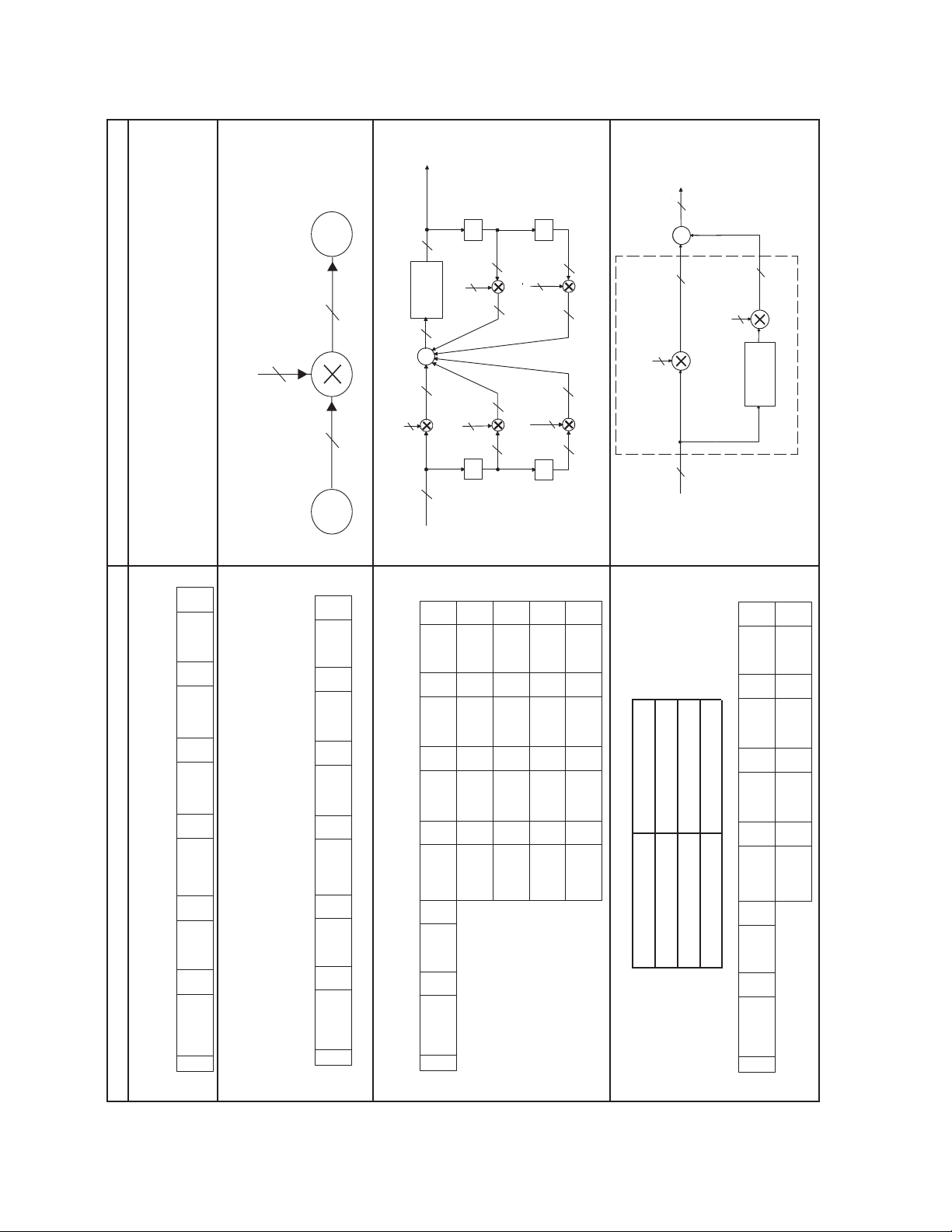
SUBADDRESS(es) PARAMETER(s)
m
0xFC – Ending I
0x00 – Starting I
s
b
S Slave Addr Ack Sub-Addr Ack xxxxxxx Ack xxxxxxxx Ack xxxxxxxx Ack xxxxxx
0x01 − 0x33
Input Mixer 28-Bit Gain Coefficients
Output Mixer 28-Bit Gain Coefficients
0x84 – 0xA1
m
s
S Slave Addr Ack Sub-Addr Ack xxx0000 Ack xxxxxxxx Ack xxxxxxxx Ack xxxxxx
1.7.2 I
1−10
b
0x34−0x4B
m
xxx0000 Ack xxxxxxxx Ack xxxxxxxx Ack xxxxxx
s
s
b
b
m
Effects Block BiQuad Filter Coefficients
S Slave Addr Ack Sub-Addr Ack xxx0000 Ack xxxxxxxx Ack xxxxxxxx Ack xxxxxx
m
xxx0000 Ack xxxxxxxx Ack xxxxxxxx Ack xxxxxx
s
b
m
xxx0000 Ack xxxxxxxx Ack xxxxxxxx Ack xxxxxx
s
b
m
xxx0000 Ack xxxxxxxx Ack xxxxxxxx Ack xxxxxx
s
b
Reverberation Block Gains
Channel 1 0x4C
Reverberation Block Subaddress
Channel 2 0x4D
Channel 3 0x4E
m
s
b
S Slave Addr Ack Sub-Addr Ack xxx0000 Ack xxxxxxxx Ack xxxxxxxx Ack xxxxxx
m
xxx0000 Ack xxxxxxxx Ack xxxxxxxx Ack xxxxxx
s
b
Page 19
b
0
b
0
48
76
76
Magnitude
48
28
48
76
76
Truncation
48
b
1
1
Truncation
b
1
a
1
28 28
z
−1
z
−1
28
28
−1
−1
Inline Gain Coeeficient
Inline Gain Coeeficient
28
Bass
Σ
Treble
Bass
Σ
Treble
(Format = 5.23)
Bypass Gain Coeeficient
Magnitude
Σ
28
z
48
a
76
76
48
z
−1
z
28
48
28
2
a
76
76
28
2
b
48
−1
z
(Format = 5.23)
Shelf Filter
Shelf Filter
28
(Format = 5.23)
Bypass Gain Coeeficient
Bass and Treble Block
NOTE: All gain coefficients 5.23 numbers
1
2
a
Ack
s
0
b
Ack
l
l
s
b
b
a
Ack
l
l
s
b
1
b
Ack
s
2
Inline Gain
Ack b
l
s
b
b
Bypass Gain
Ack
l
s
b
Ack
l
s
b
Subaddress
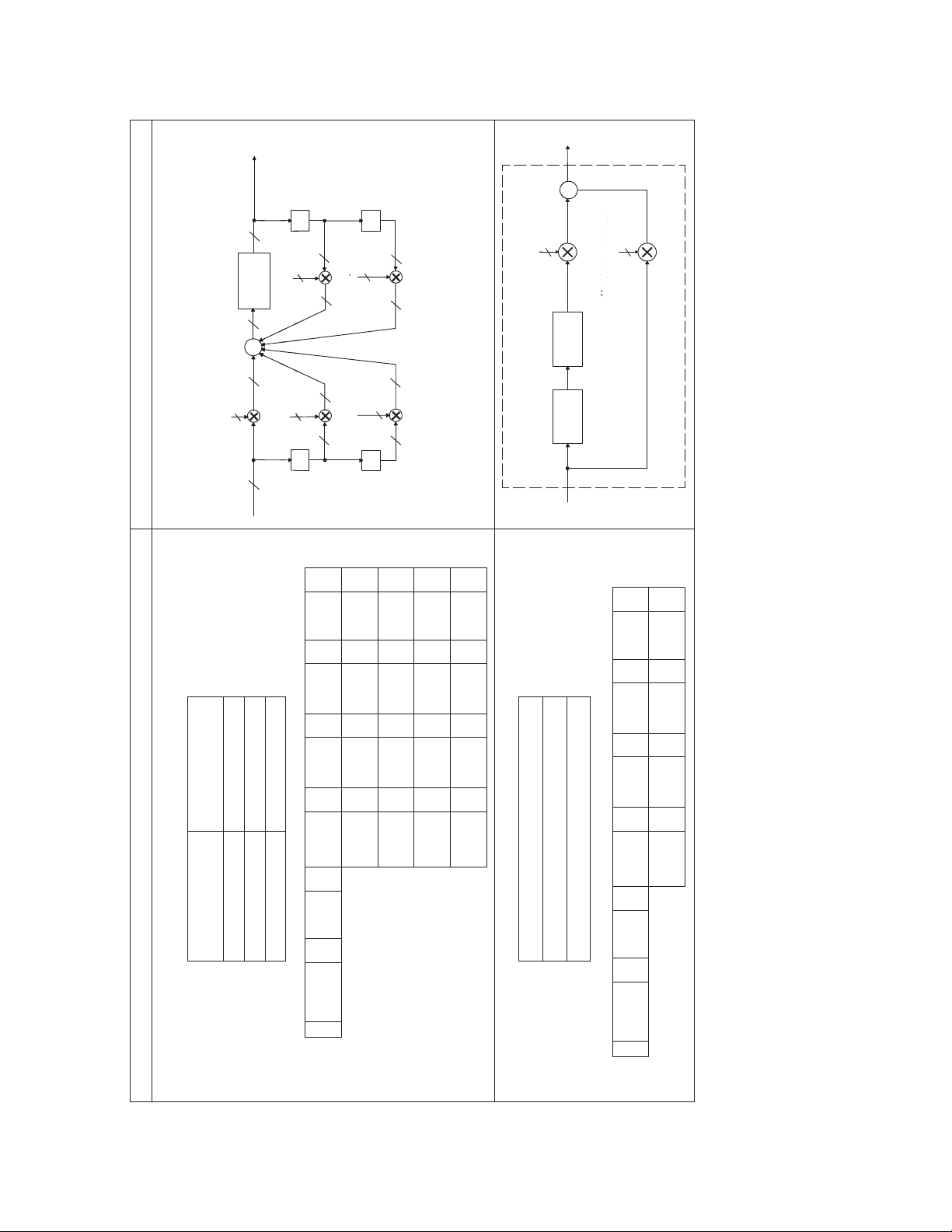
SUBADDRESS(es) PARAMETER(s)
BLOCK
Channel 1 0x4F−0x5A
Channel 2 0x5B−0x66
MAIN FILTER
Channel 3 0x67−0x72
Cascaded (Twelve/Channel) Main Filter BiQuads
m
s
b
S Slave Addr Ack Sub-Addr Ack xxx0000 Ack xxxxxxxx Ack xxxxxxxx Ack xxxxxx
m
xxx0000 Ack xxxxxxxx Ack xxxxxxxx Ack xxxxxx
s
b
m
xxx0000 Ack xxxxxxxx Ack xxxxxxxx Ack xxxxxx
s
b
m
xxx0000 Ack xxxxxxxx Ack xxxxxxxx Ack xxxxxx
s
b
m
xxx0000 Ack xxxxxxxx Ack xxxxxxxx Ack xxxxxx
s
b
Channel 1 = 0x73
Bass and Treble Gain Coefficients
s
m
Channel 2 = 0x74
Channel 3 = 0x75
S Slave Addr Ack Sub-Addr Ack xxx0000 Ack xxxxxxxx Ack xxxxxxxx Ack xxxxxx
xxx0000 Ack xxxxxxxx Ack xxxxxxxx Ack xxxxxx
s
b
b
m
1−11
Page 20
Word1
Ack
l
Ack Word2
l
s
s
b
b
m
l
Dynamic Range Control (DRC) Mixer Coefficients
s
b
m
Ack Sub-Addr Ack xxx0000 Ack xxxxxxxx Ack xxxxxxxx Ack xxxxxx
Slave Addr
S
Ack
s
b
xxx0000 Ack xxxxxxxx Ack xxxxxxxx Ack xxxxxx
s
b
Mix j to o − Inline
=
Word 1
Mix l to p − Inline
=
Word 1
Word 2 = Mix j to o − Bypass
CH1− 0x7C
Word 1 = Mix n to q − Inline
Word 2 = Mix l to p − Bypass
CH2− 0x7D
o
DRC_bypass_1
j
Loudness
Volume
CH 1 Soft
u
Word 2 = Mix n to q − Bypass
0x7E
CH1−
CH1
Σ
Mix_j_to_o_via_DRC_mult
Mix_j_to_i
Σ
Σ
Dynamic
Range Control
i
Σ
CH2
Σ
p
Mix_l_to_p_via_DRC_mult
Mix_l_to_k
l
ΣΣ
Σ
k
Loudness
v
DRC_bypass_2
Dynamic
Range Control
Volume
CH 2 Soft
CH3
q
Mix_n_to_q_via_DRC_mult
Mix_n_to_m
n
Σ Σ
m
Σ
Loudness
w
Σ
DRC_bypass_3
Volume
CH 3 Soft
1−12
m
s
b
S Slave Addr Ack Sub-Addr Ack xxx0000 Ack xxxxxxxx Ack xxxxxxxx Ack xxxxxx
= Mix j to i
0x76 = Mix u to i
0x79
CH1
= Mix l to k
= Mix v to k
0x77
0x7A
CH2
Mix_u_to_i
CH 1
Block
Bass and Treble
= Mix n to m
= Mix w to m
0x78
0x7B
CH3
Mix_v_to_k
CH 2
Bass and Treble
Block
Mix_w_to_m
CH 3
Bass and Treble
Block
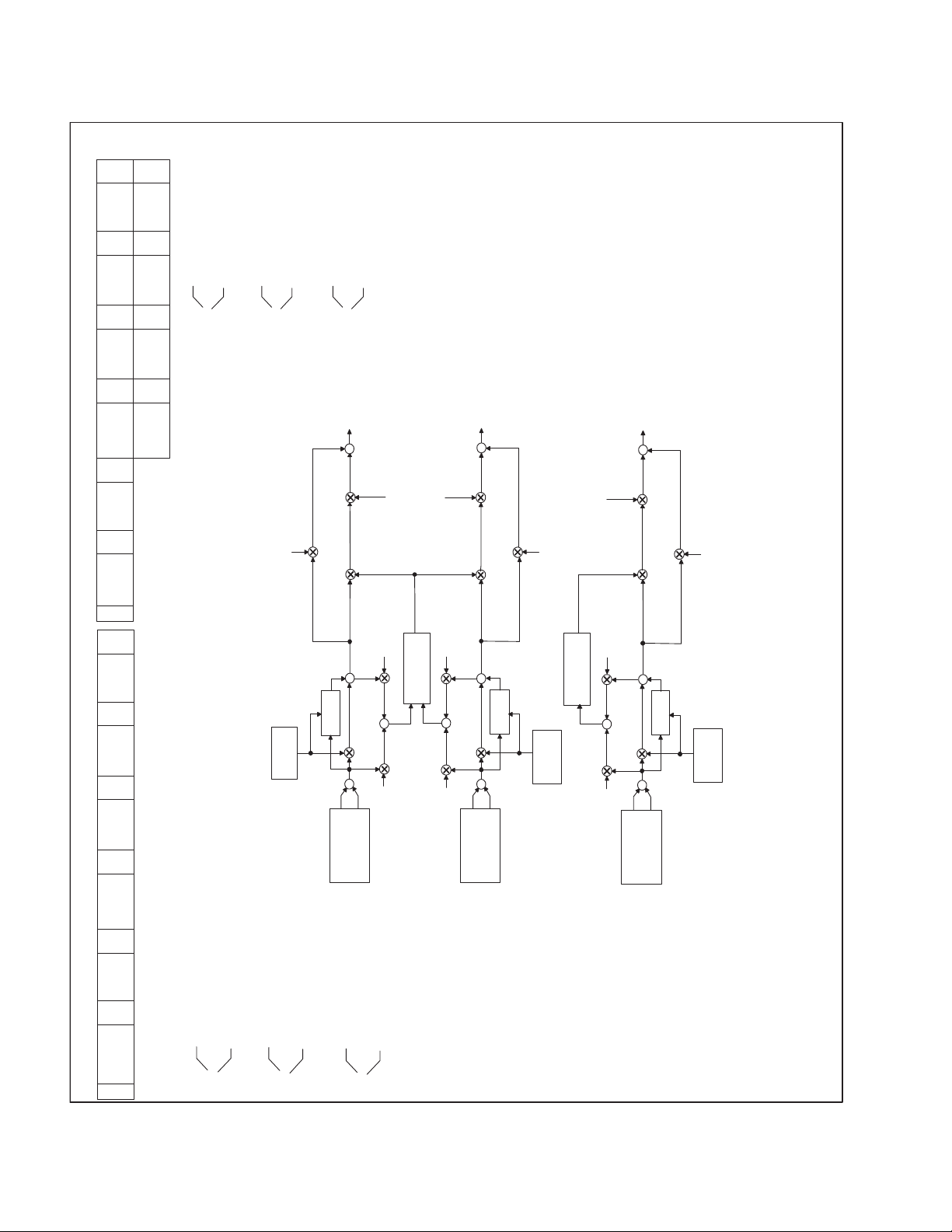
Page 21
Channel 2 0x80 = Mix Dither 2 to p − 28-Bit Coefficient
Range Control
1
Channel 2 0x80 = Mix Dither 2 to p − 28-Bit Coefficient
Range Control
3
Channel 1
Mix−Delay3_to_o
Processed Audio
Channel 2
Processed Audio
Channel 3
Processed Audio
Dither 1
Dither−Processed Audio Out _ CH
o
Σ
Channel 1
Loudness / Soft Volume
Processed Output
Ack
l
s
b
Dither 2
Mix_Dither2_to_p
Mix_Dither1_to_o
Dynamic
Dither−Processed Audio Out _ CH 2
p
Σ
Channel 2
Loudness / Soft Volume
Processed Output
Dither 3
Mix_Dither3_to_q
Dynamic
Range Control
Dither−Processed Audio Out _ CH
q
Σ
Channel 3
Loudness / Soft Volume
Processed Output
Delay 1
32-Bit Truncate
Node o
Σ
Delay 2
32-Bit Truncate
Mix−Delay3_to_o
Node p
Σ
Ack
l
s
b
Delay 3
32-Bit Truncate
Mix−Delay3_to_p
Node q
Σ
SUBADDRESS(es) PARAMETER(s)
s
b
m
Dither Mix Gain Coefficients
S Slave Addr Ack Sub-Addr Ack xxx0000 Ack xxxxxxxx Ack xxxxxxxx Ack xxxxxx
Channel 1 0x7F = Mix Dither 1 to o − 28-Bit Coefficient
Channel 3 0x81 = Mix Dither 3 to q − 28-Bit Coefficient
s
b
m
Channel 3 to Channel 1 and Channel 2 Mix Gain Coefficients
S Slave Addr Ack Sub-Addr Ack xxx0000 Ack xxxxxxxx Ack xxxxxxxx Ack xxxxxx
Channel 1 0x82 = Mix Channel 3 Output to o − 28-Bit Coefficient
Channel 2 0x83 = Mix Channel 3 Output to p − 28-Bit Coefficient
1−13
Page 22
LO MSBs
LO LSBs
Ack
lsb
xxxxxxx
lsb
G
xxxxxxx
0 MSBs
lsb
0 LSBs
Ack
xxxxxxx
Subaddress
CH1 CH2 CH3
Loudness
LG 0xA2 0xA7 0xAC
LO 0xA3 0xA8 0xAD
G 0xA4 0xA9 0xAE
O 0xA5 0xAA 0xAF
Parameter
BiQuad 0xA6 0xAB 0xB0
Soft Volume and Loudness Subaddress
LOUDNESS
CH 1 = 0xA2
CH 2 = 0xA7
VCS
AckAck Ack Ack Ack
LG
lsb
LG Is A 5.23 Format Number
CH 3 = 0xAC
xxx0000 Ack Ack Ack Ack
msb
S Slave Addr Ack Sub-Addr Ack xxxxxxxx xxxxxxxx xxxxxx
LG
( )
BiQuad Coefficients
CH 1 = 0xA3
1
a
lsb
Ack Ack Ack Ack
xxx0000
msb
CH 1 = 0xA6
CH 2 = 0xAB
CH 3 = 0xB0
S Slave Addr Ack Sub-Addr Ack xxxxxxxx xxxxxxxx xxxxxx
xxxxxxx
msb
CH 2 = 0xA8
CH 3 = 0xAD
Ack Sub-Addr Ack 00000000 Ack 00000000 Ack Ack xxxxxxxx Ack
Slave Addr
S
LO
2
a2b0b1b
lsb
lsb
xxxxxxxx xxxxxxxx xxxxxx
xxxxxxxx xxxxxxxx xxxxxx
xxx0000 Ack Ack Ack Ack
xxx0000 Ack Ack Ack Ack
msb
msb
xxxxxxxx
xxxxxxxx
LO Is A 25.23 Format Number
Ack Ack Ack
xxxxxxxx
2
lsb
lsb
xxxxxxxx xxxxxxxx xxxxxx
xxxxxxxx xxxxxxxx xxxxxx
xxx0000 Ack Ack Ack Ack
xxx0000 Ack Ack Ack Ack
msb
msb
CH 1 = 0xA4
CH 2 = 0xA9
CH 3 = 0xAE
Σ
28
0
b
xxxxxxxx
xxxxxxxx
G Is A 5.23 Format Number
xxx0000
msb
Slave Addr Ack Sub-Addr Ack Ack Ack Ack Ack
S
G
−1
z
28
1
a
28
1
b
−1
z
CH 1 = 0xA5
CH 2 = 0xAA
−1
z
28
2
a
28
2
b
−1
z
xxxxxxx
xxxxxxxxAck Ack Ack
msb
CH 3 = 0xAF
xxxxxxxx
xxxxxxxx
Ack Sub-Addr Ack 00000000 Ack 00000000 Ack Ack xxxxxxxx Ack
Slave Addr
S
O
Σ
All biquad gain coefficients 5.23 numbers.
O Is A 25.23 Format Number
AUDIO OUTAUDIO IN
Loudness Compensation
4848
48
Σ
Commanded 5.23
Volume Command
28
48
1−14
Subaddress
CH1 CH2 CH3
0xF2 0xF3 0xF4
Soft Volume
Volume Command
S Mute/Unmute = 0xF0
S Volume Slew Command = 0xF1
Parameter
Volume Command
0xF1
vcs
xxxxxxx
Ack
S Slave Addr Sub-Addr xxxxxxxx xxxxxxxx xxxxxxxx
= 2048/FS
= 4096/FS
transition
transition
SOFT VOLUME
VCS = 0 ⇒ t
VCS = 1 ⇒ t
C Master Mode
2
I
GPIO1 − Volume Down − CH1 / CH2
GPIO2 − Volume Up − CH3
GPIO3 − Volume Down − CH1 / CH2
GPIO0 − Volume Up − CH1 / CH2
Volume Commands − GPIO Terminals
Commanded
Volume
Original
Volume
C Slave Mode
2
I
transition
t
Mute / Unmute Command
0xF0
321
CCC
HHH
Ack Ack Ack Ack Ack
Slave Addr Ack Sub-Addr xxxxxxxx xxxxxxxx xxxxxxxx xxxxx
S
Volume
Command
CH 1 = 0xF2
CH 2 = 0xF3
CH 3 = 0xF4
Mute Command = 1 => 0x0000000 Volume Control
C Bus
2
Volume
I
Commands
lsb
msb
xxxxxxx
xxxxxxxx
xxxxxxxx
xxx0000
Slave Addr Ack Sub-Addr Ack Ack Ack Ack Ack
S
(LSB)
MAX
MAX
Cut
23
= x16 Boost
= 1/2
= Zero Output For 0x0000000 Volume Control
(5.23 Precision)
Volume Command
Note: Negative Volume Commands Result In Audio Polarity Inversion
Page 23
O1-MSBits
O1-LSBits
O2-MSBits
O2-LSBits
lsb
lsb
xxxxxxx
xxxxxxxx
msb
xxxxxxxx
xxxxxxx
xxxxxxx
xxxxxxxx
xxxxxxxx
xxxxxxx
msb
CH3 = 0xB9
CH1/CH2 = 0xB4
Ack xxxxxxxx Ack Ack Ack
Ack 00000000 Ack Ack Ack
Ack xxxxxxxx Ack Ack Ack
xxxxxxxx
xxxxxxxx
00000000
Ack Ack 00000000 Ack Ack Ack
Slave Addr Ack Sub-Addr 00000000
S
T1-LSBits
T2-MSBits
xxxxxxx
xxxxxxxx
msb
xxxxxxxx
xxxxxxx
T2-LSBitsxxxxxxxx
lsb
xxxxxxx
T1-MSBits
lsb
Subaddress — Dynamic Range Control (DRC) Block
xxxxxxxx
xxxxxxx
msb
CH3 = 0xB7
lsb
CH3 = 0xB8
CH1/CH2 = 0xB3
msb
K0
xxxxxxx
xxxxxxxx
xxxxxxxx
xxx0000
Ack Ack Ack Ack Ack
Slave Addr Ack Sub-Addr
S
K1
lsb
xxxxxxx
xxxxxxxx
Ack xxxxxxxx Ack Ack AckK2Ack Ack Ack Ack
xxx0000
msb
lsb
xxxxxxx
xxxxxxxx
xxxxxxxx
xxx0000
msb
msb
ae
xxxxxxxx
xxxxxxx
CH1/CH2 = 0xB2
Ack xxxxxxxx Ack Ack Ack
Ack 00000000 Ack Ack Ack
Ack xxxxxxxx Ack Ack Ack
CH3 = 0xB6
CH1/CH2 = 0xB1
xxxxxxxx
xxxxxxxx
00000000
Ack Ack 00000000 Ack Ack Ack
Ack Ack 00000000 Ack Ack Ack
lsb
xxxxxxx
xxxxxxxx
CH3 = 0xBA
CH1/CH2 = 0xB5
xxxxxxxx
xxx0000
msb
S
5.23 Format
1−ae
lsb
xxxxxxx
xxxxxxxx
Ack xxxxxxxx Ack Ack Ack
xxxxxxxx
aa
msb
Ack Ack Ack Ack Ack
Slave Addr Ack Sub-Addr
1−aa
lsb
xxxxxxx
xxxxxxxx
Ack xxxxxxxx Ack Ack AckadAck Ack Ack Ack
xxx0000
lsb
msb
xxxxxxx
xxxxxxxx
xxxxxxxx
xxx0000
1−ad
lsb
xxxxxxx
xxxxxxxx
xxxxxxxx
Ack Ack Ack Ack
xxx0000
msb
5.23 Format
25.23
Format
Compression / Expansion
Coefficient Computation
25.23
Format
Cut
Attack / Decay Control
K2
{
K1
RMS
Voltage
Estimator
32
DRC-Derived
28
O2
{
K0
Gain Coefficient
Volume
O1
Comparator
5.23 Format
a
t
x ln(1−aa)]
x ln(1−ad)]
S
S
≈ −1/[F
≈ −1/[F
a
d
t
t
d
t
T2
T1
NOTE: Compression / Expansion / Compression Displayed
= Audio Sample Frequency
S
x ln(1−ae)] Where F
S
≈ −1/[F
RMS
Voltage
Estimator
Applies to DRC Servicing CH1/CH2 Only
Window
ae and (1−ae) Set Time Window Over Which RMS Value is Computed
t
32
Slave Addr Ack Sub-Addr 00000000
S
Slave Addr Ack Sub-Addr 00000000
S
5.23 Format
Audio Input
CH1 or CH3
CH2
Audio Input
1−15
Page 24
BiQuad 1
Estimator
BiQuad 1
Estimator
RMS Voltage
Log
BiQuad 4
r
RMS Voltage
Log
s
co
RMS Voltage
od
C Bus
2
I
Log
RMS Voltage
Spectrum Analyzer / VU Meter
Log
Estimator
RMS Voltage
BiQuad 2
Log
Estimator
RMS Voltage
BiQuad 3
der
Log
Estimator
RMS Voltage
BiQuad 4
Log
Estimator
BiQuad 5
Log
Estimator
RMS Voltage
BiQuad 6
RMS Voltage
Sub-Address Dec
Log
Log
Log
Estimator
Estimator
RMS Voltage
RMS Voltage
BiQuad 7
BiQuad 8
BiQuad 9
Log
Estimator
RMS Voltage
BiQuad 10
Estimator
= Audio Sample Frequency
S
x ln(1−asa)] Where F
S
≈ −1/[F
Window
asa and (1−asa) Set Time Window Over Which RMS Value Is
Computed
t
t
s
1
2
0
1
a
b
2
b
b
1−asaAck Ack Ack Ackxxxxxxxx xxxxxxx
l
l
l
l
s
s
xxxxxxxx
Ack Ack Ack Ackxxxxxxxx xxxxxxx
xxx0000
s
m
b
b
s
xxxxxxxx
Ack Ack Ack Ackxxxxxxxx xxxxxxx
xxx0000
s
m
b
xxxxxxx
xxxxxxxx
xxx0000
s
b
m
b
b
s
xxxxxxxx
Ack Ack Ack Ackxxxxxxxx xxxxxxx
xxx0000
s
m
b
b
l
s
xxxxxxxx
Ack Ack Ack Ackxxxxxxxx xxxxxxx
xxx0000
s
m
b
b
Spectrum Analyzer/VU Meter Spectrum Analyzer/VU Meter
Ack Ack Ack Ack Ackxxxxxxxx
S Slave Addr Ack Sub-Addr a
BiQuad 1 to 10 Subaddresses = 0xBC to 0xC5
RMS Window Time Constant Subaddress = 0xBB
l
s
xxxxxxxx
xxx0000
s
m
S Slave Addr Ack Sub-Addr asaAck Ack Ack Ack Ackxxxxxxxx xxxxxxx
b
b
l
s
b
BiQuad 2
BiQuad 3
Ackxxxxx.xxx
Ackxxxxx.xxx
xxxxxxxx
xxx0000
s
b
m
S Slave Addr Ack Sub-Addr BiQuad 1Ack Ackxxxxx.xxx
Spectrum Analyzer Output Subaddress = 0xFD
BiQuad 4
Ackxxxxx.xxx
BiQuad 5
Ackxxxxx.xxx
BiQuad 6
Ackxxxxx.xxx
BiQuad 7
Ackxxxxx.xxx
BiQuad 8
Ackxxxxx.xxx
BiQuad 9
Ackxxxxx.xxx
VU Meter Output 1
VU Meter Output 1
BiQuad 10
Ackxxxxx.xxx
(BiQuad 5)
Ack Ackxxxxx.xxx
S Slave Addr Ack Sub-Addr
VU Meter Output = 0xFE
(BiQuad 6)
Ackxxxxx.xxx
1−16
Page 25
l
s
b
xxxxxxxx
0xC6
xxx0000
s
Dither Block
b
m
Distribution 2 Mix
l
s
b
xxxxxxxx
Ack Ack Ack Ackxxxxxxxx xxxxxxx
xxx0000
s
b
m
LFSR1 Mix and LFSR2 Mix Are 5.23 Format Coefficients
LFSR1
L
O
Output
− W 0 +W
0.5
Linear Feedback Shift Register Block
0.25
p
1
t
S
St2St3St4St5S
Sampler
l
s
b
LFSR2
I
C
G
Seed
LFSR1
Condensed
Seed
LFSR2
Condensed
m
l
m
xxxxxx
s
b
s
b
s
b
Seed Build Logic
0000000000000000
0xC7
t6
S Slave Addr Ack Sub-Addr Distribution 1 MixAck Ack Ack Ack Ackxxxxxxxx xxxxxxx
Σ
Dither 1
Σ
Dither 2
Σ
Dither 3
S Slave Addr Ack Sub-Addr Dither SeedAck Ack Ack Ack Ackxxxxxx
NOTE: W = 16.0 => 0x000008000000 in 25.23 Format
1−17
Page 26
Ack
70
0000000x
Ack
00000000
15 8
Ack
00000000
23 16
Ack
0xEB
31 24
Timer
1 (Default State)
Disables Watchdog
Microprocessor
Clock
Counter
Watchdog
16
Decode 2
Microprocessor
Control
Ack
210
3
GPIO_in_out
3
0000
74
Ack
GPIO and Watchdog Timer Subaddresses
0xC8−0xC9 Factory Test Subaddresses
0xD0−0xD1 CH1/CH2 to CH3 After Effects Mixers
0xCA−0xCF SDIN4 Input Mixers
SUBADDRESS(es) PARAMETER(s)
0xEF
0xD2−0xEA Reserved
Determines How Many Consecutive Logic 0 Samples
(Where Each Sample Is Spaced by GPIOFSCOUNT LRCLKs)
Are Required to Read a Logic 0 on a GPIO Input Port
Ack
GPIO_samp_int
Ack
Microprocessor
Firmware
GPIOFSCOUNT
Ack
210
GPIODIR
3
0000
Ack
31 24 23 20 19 16 15 8 7 0
Microprocessor
S Slave Addr Sub-AddrAck 00000000Ack
LD
Down
Counter
Reset
Reset
Decode 0
Microprocessor
Bus
EN
READ
C Slave Mode
2
I
DATA PATH SWITCH
Q
D
C Master Mode
2
and
I
Write
Q
Logic
Sample
D
C Master
2
I
Mode Read
Q
D
Q
D
00000000
15 8
Ack
00000000
Ack
31 24 23 16 0
S Slave Addr Sub-AddrAck 00000000Ack
0xEE
1−18
S Slave Addr Sub-AddrAck 00000000Ack
LRCLK
PWRDN
GPIO0
GPIO1
GPIO2
GPIO3
Page 27
TBLC[7:0]
Slew Rate
Treble and Bass
vsc
0000000000000000
31 24 23 16 15 8 7 0
Ack Ack Ack Ack Ackxxxxxxxx0000000
Bass
Filter Set N
0xF1—Also See Subaddress 0xA2 and Subaddress 0xF5
S Slave Addr Ack Sub-Addr
Treble
Filter Set N
= TBLC[7:0] x 1/LRCLK
Transition
t
0xEC−0xED Reserved/Factory Test Subaddresses
SUBADDRESS(es) PARAMETER(s)
0xF0—See Subaddress 0xA2 Master Mute/Un-Mute
0xEE−0xEF—See Subaddress 0xEB GPIO Port I/O Values and GPIO Parameters
0xF1
= TBLC[7:0] x 1/LRCLK
Transition
t
0xF2−0xF4—See Subaddress 0xA2 CH1−CH3 Volume CMDS
1−19
Page 28
Subaddress—Bass and Treble Shelf Filter Parameters
Treble/Bass Slew Rate Selection
(LRCLK)
Bass Filter Set Selection
S Slave Addr Ack Sub-Addr Ack Ack Ack00000xxx00000000
0xF5
Bass Shelf Selection (Filter Index)
S Slave Addr Ack Sub-Addr Ack Ack Ackxxxxxxxx00000000
0xF6
BASS
FILTER 5
S Slave Addr Ack Sub-Addr Ack Ack Ack0000000000000000
0xF1
CH3
Treble Filter Set Selection
S Slave Addr Ack Sub-Addr Ack Ack Ack00000xxx00000000
0xF7
Treble Shelf Selection (Filter Index)
S Slave Addr Ack Sub-Addr Ack Ack Ackxxxxxxxx00000000
0xF8
BASS
FILTER 3
BASS
FILTER 1
CH2
MAX BOOST
SHELF
MID-BAND
CH1
Ack00000xxx
CH1CH2CH3
Ackxxxxxxxx Ackxxxxxxxx
TREBLE
FILTER 5
Ack00000xxx
CH3
CH3
TREBLE
FILTER 3
V
Ack0000000 Ackxxxxxxxx
C
S
Treble/Bass Slew Rate = TBLC
(Slew Rate = TBLC/FS,
Where FS = Audio Sample Rate)
CH2
Ack00000xxx
CH2
TREBLE
FILTER 1
CH1
Ackxxxxxxxx Ackxxxxxxxx
07
CH1
Ack00000xxx
BASS
FILTER 4
Treble & Bass Filter Set Commands
0 => No Change
1 − 5 => Filter Sets 1 − 5
6 − 7 => Illegal (Behavior Indeterminate)
BASS
FILTER 2
MAX CUT
SHELF
FREQUENCY
TREBLE
FILTER 4
Treble & Bass Filter Shelf Commands
0 => Illegal (Behavior Indeterminate)
1 − 150 => Filter Shelves 1 − 150
1 => +18-dB Boost
150 => −18-dB Cut
151 − 255 => Illegal (Behavior Indeterminate)
TREBLE
FILTER 2
3-dB CORNERS (kHz)
FS
FILTER SET 5 FILTER SET 4 FILTER SET 3 FILTER SET 2 FILTER SET 1
BASS TREBLE BASS TREBLE BASS TREBLE BASS TREBLE BASS TREBLE
96 kHz 0.25 6 0.5 12 0.75 18 1 24 1.5 36
88.4 kHz 0.23 5.525 0.46 11.05 0.691 16.575 0.921 22.1 1.381 33.15
64 kHz 0.167 4 0.333 8 0.5 12 0.667 16 1 24
48 kHz 0.125 3 0.25 6 0.375 9 0.5 12 0.75 18
44.1 kHz 0.115 2.756 0.23 5.513 0.345 8.269 0.459 11.025 0.689 16.538
32 kHz 0.083 2 0.167 4 0.25 6 0.333 8 0.5 12
24 kHz 0.063 1.5 0.125 3 0.188 4.5 0.25 6 0.375 9
22.05 kHz 0.057 1.378 0.115 2.756 0.172 4.134 0.23 5.513 0.345 8.269
16 kHz 0.042 1 0.083 2 0.125 3 0.167 4 0.25 6
12 kHz 0.031 0.75 0.063 1.5 0.094 2.25 0.125 3 0.188 4.5
11.025 kHz 0.029 0.689 0.057 1.378 0.086 2.067 0.115 2.756 0.172 4.134
1−20
Page 29
18 Bit
20 Bit
24 Bit
32 Bit
32 Bit
32 Bit
1
1
1
32 Bit
16 Bit
Word Size
0101010
IW0/OW0
†
0011001
IW1/OW1
Word Size Code
0000111
AB assigns TDM time slots for those TDM
outputs involving two TAS3103s. For these
output formats, one of the TAS3103 chips
must be defined as AB = 0. The other
C M AND N ASSIGNMENTS
2
IW2/OW2
TAS3103 chip must be defined as AB = 1.
Input and output word sizes are
†
independent.
MCLKI
OSC
XTALO
CRYSTAL
XTALI
0
MUX
MCLKO
PLL0
PLL[1:0]
PLL1
14 13 11 10 8
DWFMT (Data Word Format)
15
÷2
÷4
1
2
3
÷2
÷4
0
1
2
MUX
x11
PLL
0
1
2
3
MUX
OW[2:0]
IW[2:0]
AB
PLL
BYPASS
0xF9
0
7
815
161819212223242627282931
AckIOMAck
DWFMT
Ackz[2:0]IMS x[2:0]ICSAck x[2:0]y[2:0]w[1:0]000AckSub-AddrAckSlave AddrS
OM[3:0]IM[3:0]
743 0
÷2
0
1
0
S)
2
S
2
Mode
Discrete, Left Justified
Discrete, Left Justified
Discrete, Right Justified
Discrete, I
Discrete, 16 − Bit Packed
TDM_LJ_8
TDM_LJ_6
TDM_LJ_4
TDM_I2S_8
TDM_I2S_6
TDM_I2S_4
TDM_20Bit_6
6 Ch, Single Chip, Crystal (LJ)
6 Ch, Single Chip (LJ)
6 Ch, Single Chip, Crystal (I
6 Ch, Single Chip, 20 − Bit
‡
IM0/OM0
IM1/OM1IM2/OM2IM3/OM3
÷16
÷4
÷32
÷8
2
3
4
1
÷2
÷8
÷4
1
2
3
0
5
÷16
4
6
÷32
5
7
MUX
6
1
0
Serial Audio Port (AP) Mode Code
0 0 0 0
0 0 0 1
MUX
SCLKIN
7
MUX
0
MUX
1
MUX
0 0 1 0
0 0 1 1
0 1 0 0
0 1 0 1
0 1 1 0
0 1 1 1
1 0 0 0
1 0 0 1
1 0 1 0
1 0 1 1
1 1 0 0
1 1 0 1
Input and output mode selections are independent.
‡
1 1 1 0
1 1 1 1
S FORMAT, CLOCK MANAGEMENT, AND I
2
I
MICROCLK_DIV
I2C_SDA
I2C_SCL
Clock
Processor
Digital Audio
1
Clock
C
2
Microprocessor
I
Sampling
÷4
0
Clock
SCLKOUT2 SCLKOUT1
÷128
÷192
÷256
÷512
0
÷64
1
2
3
4
÷384
5
6
7
MUX
LRCLK
÷32
Ack
02
n[2:0]
m[3:0]
C
2
I
Master
SCL
0xxxxxxx
Ack
00000000
Ack
00000000
MUX
36
N
÷2
1/(M+1)
÷10
C
2
I
Module
0xFB
00000000
Ack
Sub-AddrAckSlave AddrS Ack
See Section 2.1.1 for a detailed discussion of this restriction.
NOTE: F9 must not be updated without first muting all three monaural channels in the TAS3103.
1−21
Page 30
Delay/Reverb Assignments
0xFA
Delay Reverb
Delay Channel 1 = 2 x {D1[11:0] + 1}
Delay Channel 2 = 2 x {D2[11:0] + 1}
Delay Channel 3 = 2 x {D3[11:0] + 1}
Reserved
m
S Slave Addr Ack Sub-Addr D1 and R1Ack Ack Ack Ack Ackxxxxxxx
xxx0000
s
b
m
xxx0000
Ack Ack Ack Ack
s
b
m
xxx0000
s
b
xxxxxxx
xxxxxxx
xxxxxxx
l
s
b
l
s
b
l
s
b
m
xxx0000
s
b
m
xxx0000
s
b
m
s
b
xxxxxxx
xxx0000
Note: 2 x (D1 + D2 + D3) + 3 x (R1 +R2 +R3) ≤ 4076
l
s
b
l
s
D2 and R2
b
l
D3 and R3Ack Ack Ack Ackxxxxxxx
s
b
Reverb Channel 1 = 2 x {R1[11:0] + 1}
Reverb Channel 2 = 2 x {R2[11:0] + 1}
Reverb Channel 3 = 2 x {R3[11:0] + 1}
Reserved
NOTE: Changes in reverb and delay assignments can result in unplesasant and extended audio artifacts.
It is recommended that the TAS3103 always be muted before making reverb and delay changes.
See section 3.6.3 for a detailed discussion of this restriction.
1−22
Page 31

SUB-ADDRESS(ES)
0xFF—Volume Busy Flag
PARAMETER(S)
0xFC—See Subaddress 0x00 Ending I2C Check Word
0xFD−0xFE—See Subaddress 0xBB Spectrum Analyzer/VU Meter Ouputs
Volume
S Slave Addr Ack Sub-Addr Ack Ack0000000x
Flag
S Volume Flag = 0 ⇒ No volume commands are active.
S Volume Flag = 1 ⇒ One or more volume commands are
active.
1−23
Page 32

1−24
Page 33

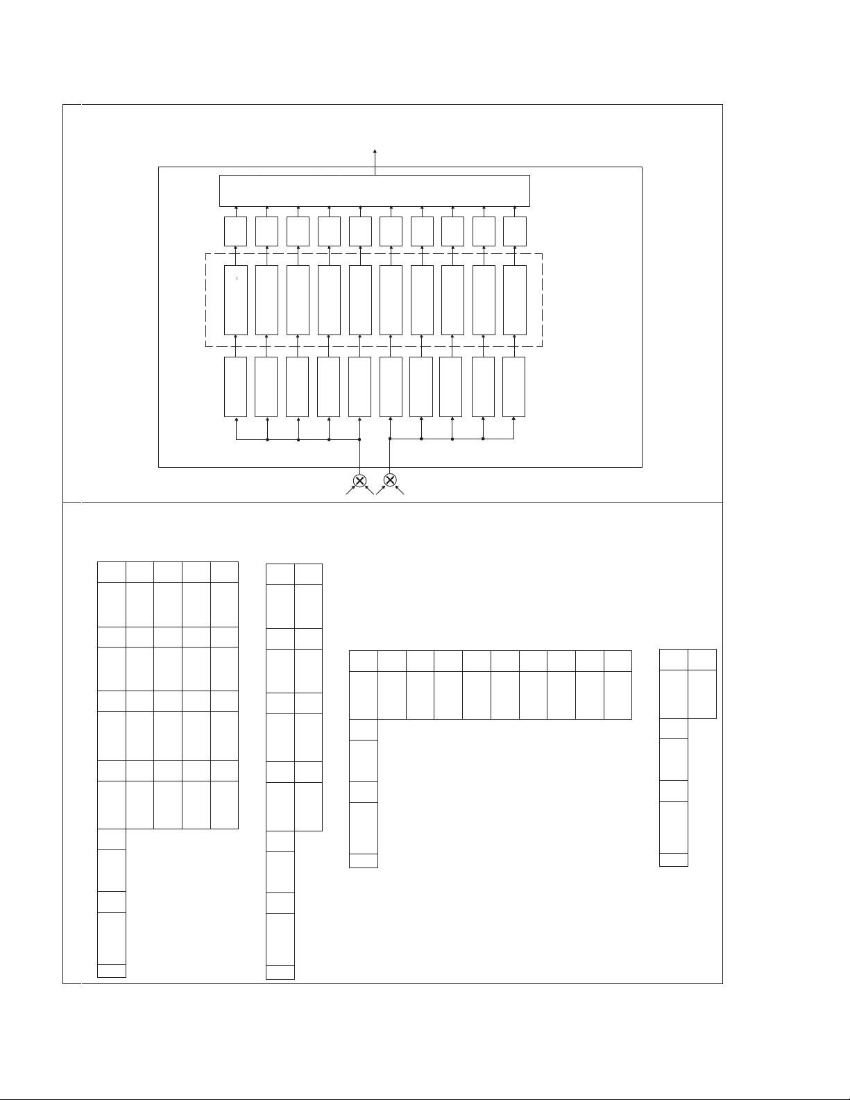
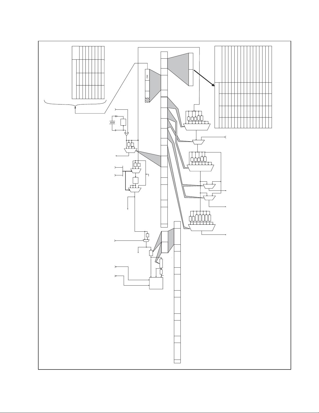
2 Hardware Architecture
Figure 2−1 depicts the hardware architecture of the chip. The architecture consists of five major blocks:
• Input Serial Audio Port (SAP)
• Output Serial Audio Port (SAP)
• DPLL and Clock Management
• Controller
• Digital Audio Processor (DAP)
2−1
Page 34

SDIN1
3
2
1
SCLKIN
MCLKI XTALI XTALO
OSC
MCLK
MCLKO PLL1 PLL0 SCLKOUT1 LRCLK MICROCLK_DIV SCLKOUT2
M
U
÷2
÷2
÷Z
M
U
X
÷X
÷Y
X
÷2
M
PLL
U
X
÷4
M
U
X
ORIN
M
U
(x11)
X
÷2
M
U
X
M
U
X
SDIN2
SDIN3
SDIN4
32 Bits
32 Bits
32 Bits
32 Bits
32 Bits
32 Bits
32 Bits
Reg
INPUT SAP
PLL and Clock Management
4K x 16
Delay Line
RAM
Controller
Master/Slave
Controller
I2C
Dual Port
Data RAM
Arithmetic
Engine
76-Bit Adder
Regs
Volume
Update
Oversample Clock
Master
SCL
÷10
Coefficient
RAM
1/(M+1)
Instruction Decoder/Sequencer
Digital Audio Processor
Regs
Arithmetic Unit
2K x 8
Data
RAM
N
1/2
256 x 8
Data
RAM
Program
ROM
DAP
(DAP)
16K x 8
Program
ROM
8-Bit
WARP
8051 Microprocessor
256 Bits
64 Bits
64 Bits
Reg
OUTPUT SAP
SDOUT
SDOUT
SDOUT
2−2
I2C_SDA
CS0 CS1I2C_SCL GPIO1 GPIO2 GPIO3
I2CM_S
GPIO0
Figure 2−1. TAS3103 Detailed Hardware Block Diagram
Page 35

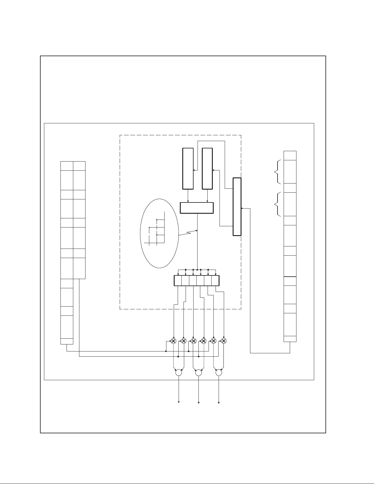
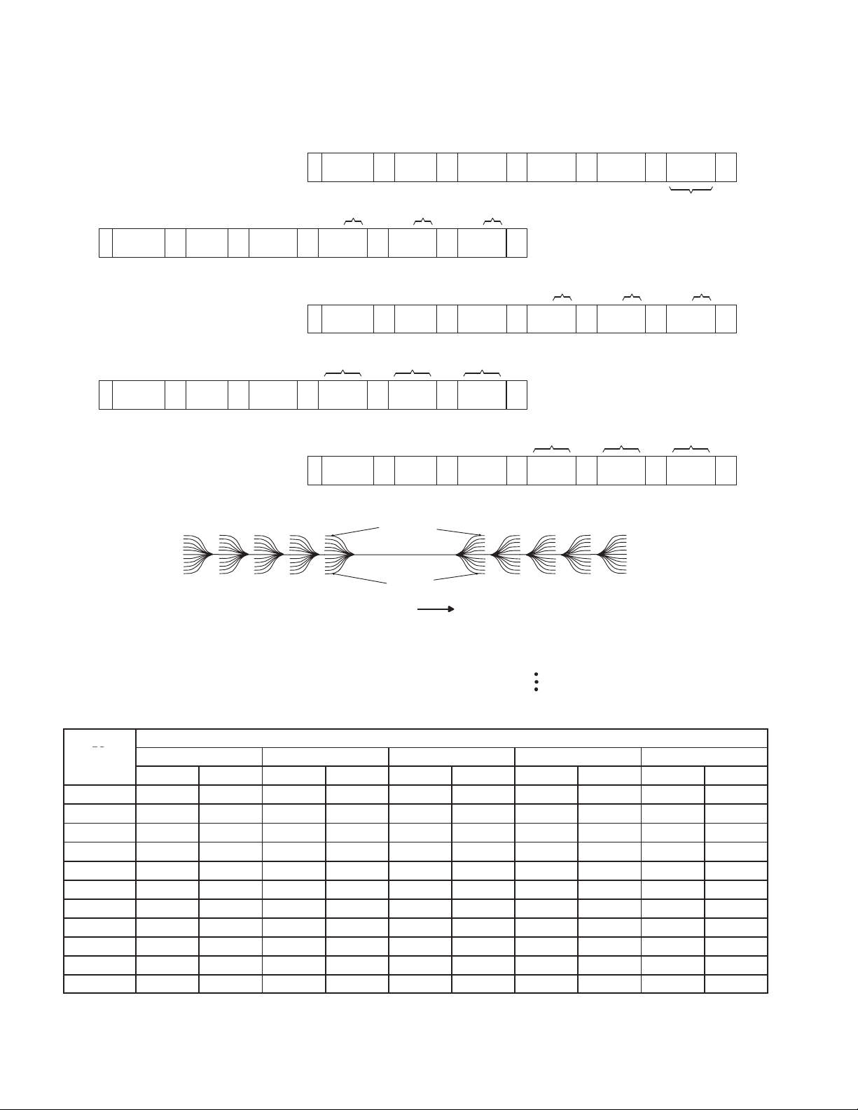
2.1 Input and Output Serial Audio Ports (SAPs)
L
The TAS3103 accepts data in various serial data formats including left/right justified and I2S, 16 through 32 bits,
discrete, or TDM. Sample rates from 8 kHz through 96 kHz are supported. Each TAS3103 has four input serial ports
and three output serial ports, labeled SDIN[4:1] and SDOUT[3:1] respectively. All ports accommodate stereo data
formats, and SDIN1 and SDOUT1 also accommodate time-division multiplex (TDM) data formats. The formats are
selectable via I
the same format; and the two formats need not be the same. The TAS3103 can accommodate system architectures
that require data format conversions without the need for additional glue logic. If a TDM format is selected for the input
port, only SDIN1 is active; the other three input channels cannot be used. If a TDM format is selected for the output
port, only SDOUT1 is active; the other two channels cannot be used.
2.1.1 SAP Configuration Options
The TAS3103 serial interface data format options for discrete (stereo) data are detailed in Figure 2−2.
Left / Right
Justified
RCLK
Left Justified
2
C commands. All input channels are assigned the same format and all output channels are assigned
2
I
S
SCLK
Bit 31
MSB
MSB−1
LSB+1
LSB
Bit 0
Bit 31 Bit 0
MSB−1 MSB
LSB
Bit 31
MSB−1 MSB
SCLK
Right Justified
SCLK
Bit 31 Bit 31
MSB−1 MSB MSB−1 MSB
Bit 0
2
I
S
Bit 0 Bit 0
LSB
LSB+1
Bit 0 Bit 31Bit 31
LSB+1LSB LSB+1 MSB−1 MSB MSB−1 MSB
LSB
LSB+1
LSB
Bit 31
Bit 0
Bit 31
MSB
Figure 2−2. Discrete Serial Data Formats
When the TAS3103 is transmitting serial data, it uses the negative edge of SCLK to output a new data bit. The
TAS3103 samples incoming serial data on the rising edge of SCLK.
The TDM modes on the TAS3103 only provide left justified and I
2
S formats, and each word in the TDM data stream
adheres to the bit placement shown in Figure 2−2. Figure 2−3 illustrates the output data stream for a 4-channel TDM
mode. T w o cases are illustrated; an I
2
S data format case (SAP output mode 1010) and a left-justified data format case
(SAP output mode 0111).
Justified
LRCLK
Left
Data
MSB MSB−1MSB MSB−1MSB MSB−1MSB
LRCLK
I2S
Data
Left Channel 1 Left Channel 2 Right Channel 1 Right Channel 2
MSB−1 LSB LSB LSB LSB MSB
Left Channel 1 Left Channel 2 Right Channel 1 Right Channel 2
MSB−1MSB MSB−1MSB MSB−1MSB
LSBLSBLSBLSBMSB−1MSB
Figure 2−3. Four-Channel TDM Serial Data Formats
2−3
Page 36

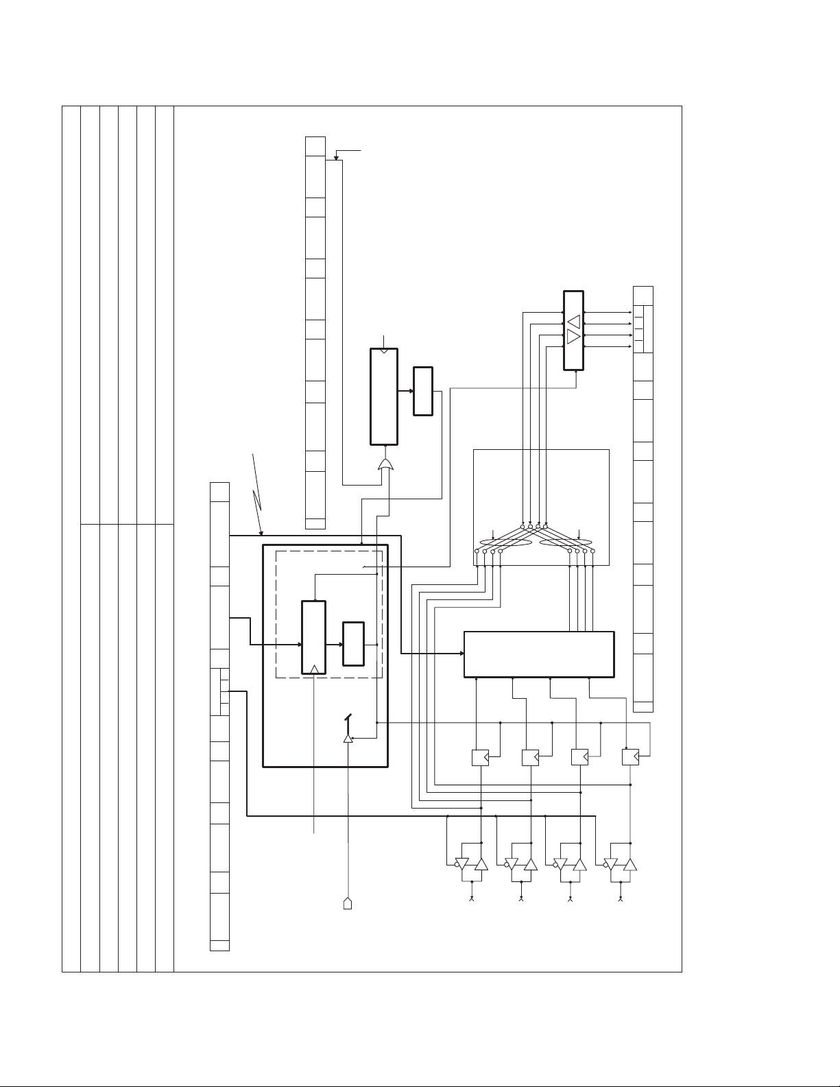
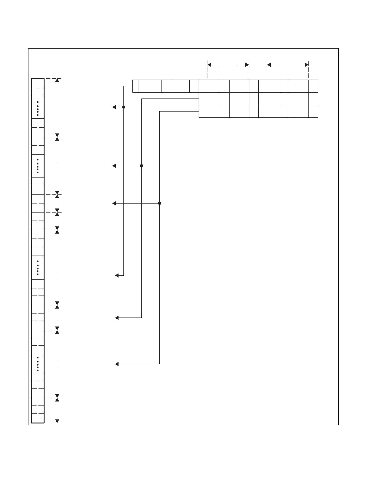
A 16-bit field contained in the 32-bit word located at I2C subaddress 0xF9 configures both the input and output serial
audio ports. Figure 2−4 illustrates the format of this 16-bit field. The data is shown in the transmitted I
2
C protocol
format, and thus, in addition to the data, the start bit S, the slave address, the subaddress, and the acknowledges
required by every byte are also shown.
Output Port
TDM Alignment
Input Port
Word
Size
Output Port
Word
Size
0xF9
2431
15
14 13 11 10 8
AB
1623
AckxxxxxxxxAckSub-AddrAckSlave AddrS
xxxxxxxxAck
OW[2:0]
IW[2:0]
DWFMT
743 0
Format
DWFMT (Data Word Format)
7
815
IOMAck
OM[3:0]IM[3:0]
Output
Input
Port
Port
Format
0
Ack
Figure 2−4. SAP Configuration Subaddress Fields
Commands to reconfigure the SAP cannot be issued as standalone commands, but must accompany mute and
unmute commands. The reason for this is that an SAP configuration change while a volume or bass or treble update
is taking place can cause the update to not properly be completed. Figure 2−5 shows the recommended procedure
for issuing SAP configuration update commands.
After a reset, ensure that 0xF9 is written before volume, treble, or bass.
2−4
Page 37

Enter
Yes
Issue Mute Command
Yes
Issue SAP Configuration
Issue Un-Mute Command
Vol
Busy
No
Vol
Busy
No
Change Command
Yes
Vol
Busy
Exit
No
Mute Command = 0x00000007 at subaddress x0F0
Un-mute command = 0x00000000 at subaddress 0xF0
SAP configuration subaddress = 0x59
Volume busy flag = LSB of subaddress 0xFF. Logic 1 = busy
Figure 2−5. Recommended Procedure for Issuing SAP Configuration Updates
Figure 2−6, Figure 2−7, and Figure 2−8 tabularize the formatting and word size options available for the input SAP
and output SAP. In these figures, data formats are paired when the only difference between the pair is whether the
word placement within the LRCLK period is left justified or I
output formats (SDOUT1
SDOUT1
). For two chip TDM output formats, the OR’ing operation is accomplished by routing SDOUT1 from
chipB
or SDOUT1
chipA
) and two chip TDM output formats (SDOUT1
chipB
2
S. The TDM formats available include single chip TDM
OR’ed with
chipA
one of the two T AS3103 chips to ORIN of the other TAS3103 chip. The AB bit also comes into play for two chip TDM
formats; AB must be set to 1 on one of the two TAS3103 chips and set to 0 on the other TAS3103 chip. For a given
connection of SDOUT1 to ORIN, it does not matter which TAS3103 is set up as chip AB = 1 and which chip is set
up as chip AB = 0. However, the routing of the processed data to the output registers in the TAS3103 is dependent
on which chip is chip AB = 0 and which chip is chip AB = 1. Figure 2−10 and Figure 2−11 illustrate this dependence.
2−5
Page 38

In Figure 2−10 and Figure 2−11, the paired TDM output formats 0101 and 1000 are unique in that each format, in
effect, services two distinct industry formats. For these two modes, if register Y in chip AB = 1 is set to zero (by
appropriate output mixer coefficient settings), the resulting format is a standard 8 CH TDM format. This option is
illustrated in Figure 2−7.
2−6
Page 39

INPUT
IM[3:0]
FORMAT
WORDSIZE
INPUT
IM[3:0]
FORMAT
WORDSIZE
LR
LR
LR
AB
LR
DISCRETE
DISCRETE
DIVISION
DIVISION
EF
32 32
LR
CD
32 32
LR
SDIN1 SDIN2 SDIN3
AB
32 32
LR
DATA DISTRIBUTION: A, B, C, D, E, F, G, H = INPUT MIXER INPUTS
Not available Not available
AB
16 16
LR
Not available Not available
Not available Not available
GECAHFDB
32 32 32 32 32 32 32 32
Not available Not available
Not available Not available
Not available Not available
Not available Not available
DB
FDB
32 32 32
LR
LR
ECA
32 32 32
32 32
CA
32 32
LR
Not available Not available
Not available Not available
FDB
20 20 20 4
LR
ECA
20 20 20 4
Not available Not available
ECA FDB
32 32 32 32 32 32 32 32
S and left justified—for the 6 Ch input
2
Left justified All options valid
(1)
000X
TYPE
S All options valid except 32 bit
2
0011 I
0010 Right justified All options valid
0100 16-bit packed IW[2:0] = 001
All options valid
S All options valid except 32 bit
2
8 CH transfer, left
justified
0101
1000 8 CH transfer, I
0110/1101
S All options valid except 32 bit
2
6 CH, left justified All options valid
6 CH, I
(3)
(2)(3)
0111 4 CH, left justified All options valid
1001
TIME
S All options valid except 32 bit
2
6 CH, 20 bit IW[2:0] = 011
(4)
1010 4 CH, I
1011/1111
(TDM)
MULTIPLEX
All options valid
All options valid except 32 bit
S
2
6 CH data, 8 CH
transfer, left justified
6 CH data, 8 CH
transfer, I
1110
1100
S and left justified—made for the 6 CH output SAP.
2
Figure 2−6. Format Options: Input Serial Audio Port
SAP can be made independent of the data format selections—I
2. IM[3:0] modes 0110 and 1101 are identical for the input SAP. OM[3:0] modes 0110 and 1101 do produce different results in the output SAP (see Figure 2−7).
NOTES: 1. Left justified, stereo is the default input format.
4. IM[3:0] modes 1011 and 1111 are identical for the input SAP. OM[3:0] modes 1011 and 1111 do produce different results in the output SAP (see Figure 2−7).
3. If a 6 CH input format is selected, the output format must also be set to 6 CH. When in a 6 CH mode, data format selections—I
2−7
Page 40

OUTPUT
OM[3:0]
FORMAT
WORDSIZE
OUTPUT
OM[3:0]
FORMAT
WORDSIZE
Not available Not available
TIME
Not available Not available
Not available Not available
Not available Not available
Not available Not available
Not available Not available
Not available Not available
VW
Not available Not available
Not available Not available
Not available Not available
Not available Not available
S and left justified—for the output SAP can
2
SDOUT1 SDOUT2 SDOUT3
LR
UAB = 0 V W X
32 32 32 32 32 32 32 32
LR
32 32 32 32 32 32 32 32
DATA DISTRIBUTION: U, V, W, X, Y, Z = OUTPUT MIXER OUTPUTS
AB = 1 U V W Y X
All options valid
S All options valid except 32 bit
2
UAB = 0 V W
32 32 32 32 32 32
AB = 1 U WY
All options valid
S All options valid except 32 bit
2
WX
32 32
LR
UV
32 32
32 32 32 32 3232
S All options valid except 32 bit
2
W
LR
UV
AB = 0
OW[2:0] = 011
20 20 20 4
20 20 20 4
U
20 20 20 4
AB = 1
LR
V Y
20 20 20 4
UAB = 0 W X Z
32 32 32 32 32 32 32 32
All options valid
All options valid except 32 bit
XYZ
32 32 32
LR
UVW
32 32 32
XYZ
20 20 20 4
LR
UVW
20 20 20 4
All options valid
S and left justified—can be made for the input SAP.
2
Figure 2−7. TDM Format Options: Output Serial Audio Port
2−8
8 CH, 2 chip, left
TYPE
justified
0101
6 CH, 2 chip, left
justified
(1)
1000 8 CH, 2 chip, I
0110
6 CH, 2 chip, I
(1)
0111 4 CH, left justified All options valid
1001
1010 4 CH, I
TIME
1011 6 CH, 2 chip,
(TDM)
DIVISION
MULTIPLEX
20 bit
6 CH data,
8 CH transfer,
left justified
1100
S
2
6 CH data,
8 CH transfer,
I
1110
6 CH,
left justified
(1)
1101
1111 6 CH, 20 bit OW[2:0] = 011
be made independent of the data format selections—I
NOTE 1: If a 6 CH output format is selected, the input format must also be set to 6 CH. When in a 6 CH mode, data format selections—I
Page 41

OUTPUT
OM[3:0]
FORMAT
WORDSIZE
OUTPUT
OM[3:0]
FORMAT
WORDSIZE
LR
UV
LR
WX
LR
YZ
DISCRETE
YZ
DISCRETE
SIZE
SAMPLE
32 32
LR LR
WX
32 32
Not available Not available
LR
LR
SDOUT1 SDOUT2 SDOUT3
UV
32 32
UV
DATA DISTRIBUTION: U, V, W, X, Y, Z = OUTPUT MIXER OUTPUTS
16 16
Left justified All options valid
(1)
000X
TYPE
S All options valid except 32 bit
2
0011 I
0010 Right justified All options valid
0100 16-bit packed OW[2:0] = 001
INPUT IW[2:0] OUTPUT OW[2:0]
IW2 IW1 IW0 OW2 OW1 OW0
SIZE
SAMPLE
(32) 0 0 0 0 0 0
18 Bit 0 1 0 0 1 0
20 Bit 0 1 1 0 1 1
(32) 1 1 0 1 1 0
24 Bit 1 0 0 1 0 0
(32) 1 1 1 1 1 1
32 Bit 1 0 1 1 0 1
DEFAULT → 16 Bit 0 0 1 0 0 1
(32) ⇒ Reserved for future family members. Selection of 000, 110, or 111 in the
Figure 2−8. Discrete Format Options: Output Serial Audio Port
TAS3103 selects a 32-bit sample size.
NOTE 1: Left justified, stereo is the default input format.
Figure 2−9. Word Size Settings
2−9
Page 42

TAS3103
SDOUT1
U1
(AB = ’1’)
ORIN
TAS3103
SDOUT1
U2
(AB = ’0’)
ORIN
LRCLK
U2 V W X
U1 U V W 0 X
LR
U
32 32 32 32 32 32 32 32
32 32 32 32 32 32 32 32
LRCLK
SDOUT1
LR
U
UU1V
U2
U1
32 32 32 32 32 32 32 32
V
U2
W
U1
U2
X
W
U1
X
U2
U1
Figure 2−10. 8 CH TDM Format Using SAP Modes 0101 and 1000
TAS3103
SDOUT1
U1
(AB = 0)
ORIN
TAS3103
SDOUT1
U2
(AB = 1)
ORIN
LRCLK
U1 V W 0
U2 U 0 W Y 0
LR
U
32 32 32 32 32 32 32 32
32 32 32 32 32 32 32 32
LRCLK
SDOUT1
LR
U
U1
32 32 32 32 32 32 32 32
U1
UU2V
U1
W
U1
Y
W
U2
U2
Figure 2−11. 6 CH Data, 8 CH Transfer TDM Format Using SAP Modes 0101 and 1000
For these same two modes, if register X in chip AB = 0 is set to zero, and registers V and X in chip AB = 1 are set
to zero, the resulting format is a 6 CH data, 8 CH transfer format. This option is shown in Figure 2−11.
The data output format in Figure 2−11 is identical to that realized using data output formats 1100 and 1110 in
Figure 2−7. The difference is that SAP modes 1010 and 1000 provide six independent monaural channels to process
the data, whereas SAP modes 1100 and 1 110 provide only three independent monaural channels to process the data.
2.1.2 Processing Flow—SAP Input to SAP Output
All SAP data format options other than I2S result in a two-sample delay from input to output, as illustrated in
Figure 2−12. Figure 2−12 is also relevant if I
polarity of LRCLK in Figure 2−12 has to be inverted in this case). However, i f I
between input and output, the delay becomes either 1.5 samples or 2.5 samples, depending on the processing clock
frequency selected for the digital audio processor (DAP) relative to the sample rate of the incoming data. The input
to output delay for an I
illustrates the delay for a non-I
2
S input format and a non-I2S output format is illustrated in Figure 2−13(a), and Figure 2−13(b)
2
S input format and an I2S output format. In each case, two distinct input to output delay
times are shown: a 1.5 sample delay time if the processing time in the DAP is less than half the sample period, and
a 2.5 sample delay time if the processing time in the DAP is greater than half the sample period.
The departure from the two-sample input to output processing delay when I
due to the use of a common LRCLK. The I
all other formats use the rising edge of LRCLK to begin a sample period. This means that the input SAP and digital
audio processor (DAP) operate on sample windows that are 180° out of phase with respect to the sample window
used by the output SAP. This phase difference results in the output SAP outputting a new data sample at the midpoint
of the sample period used by the DAP to process the data. If the processing cycle completes all processing tasks
before the midpoint of the processing sample period, the output SAP outputs this processed data. However, if the
processing time extends past the midpoint of the processing sample period, the output SAP outputs the data
processed during the previous processing sample period. In the former case, the delay from input to output is 1.5
samples. In the latter case, the delay from input to output is 2.5 samples.
2
S formatting is used for both the input SAP and the output SAP (the
2
S format uses the falling edge of LRCLK to begin a sample period, whereas
2
S format conversions are performed
2
S format conversions are performed is
2−10
Page 43

SDOUT1
U
SDOUT2
V
W
SDOUT3
X
Y
Z
SDOUT1
SDOUT2
U
V
WW
SDOUT3
X
Y
Z
Half − Sample Time N
nd
2
Sample Time N + 1 Sample Time N + 2
Sample Time N
Input
Input
Serial
Regs
Holding
Regs
Holding
Rx
Regs
A
SDIN1
SDOUT1
U
Channel 1
Channel 2
Channel 3
Sample Time N + 1 Sample Time N + 2
Channel 1
Channel 2
Channel 3
Sample Time N + 2
B
SDOUT2
C
SDIN2
D
SDOUT3
E
SDIN3
F
G
SDIN4
H
Sample Time N
Input
Input
Serial
Regs
Holding
Regs
Holding
Rx
Regs
SDOUT1
A
SDIN1
B
C
SDIN2
SDOUT2
D
SDOUT3
E
SDIN3
F
H
G
SDIN4
Figure 2−12. SAP Input-to-Output Latency
V
X
Y
W
Z
U
V
X
Y
Z
Half − Sample Time N
st
1
Sample Time N + 1 Sample Time N + 2
Sample Time N
Input
Input
Serial
Regs
Holding
Regs
Holding
Rx
Regs
A
SDIN1
Channel 1
Channel 2
Channel 3
Sample Time N + 1 Sample Time N + 2
Channel 1
Channel 2
Channel 3
Sample Time N + 1
B
C
SDIN2
D
E
SDIN3
F
G
SDIN4
H
Sample Time N
Input
Input
Serial
Regs
Holding
Regs
Holding
Rx
Regs
A
SDIN1
B
C
SDIN2
D
E
SDIN3
F
H
G
SDIN4
2−11
Page 44

LRCLK
2.5
Cycle
Delay
1.5
Cycle
Delay
SDIN
Processing Cycle
Load Output Holding Registers
Holding Register ⇒ Output Serial Registers
SDOUT
Processing Cycle
Load Output Holding Registers
Holding Register ⇒ Output Serial Registers
SDOUT
(a) Left-Justified Input / I2S Output
LRCLK
SDIN
L2
L1, R1
L1, R1 L2, R2
R0
L2
R2 L3 R3 L4 R4
L0 R0 L1 R1 L2
L1 R1 L2 R2 L3
R2 L3 R3 L4 R4
L2, R2 L3, R3
L3, R3
2.5
Cycle
Delay
1.5
Cycle
Delay
Processing Cycle
Load Output Holding Registers
Holding Register ⇒ Output Serial Registers
SDOUT
Processing Cycle
Load Output Holding Registers
Holding Register ⇒ Output Serial Registers
SDOUT
L1, R1
L0 R0 L1 R1 L2
L1, R1 L2, R2
R0
L1 R1 L2 R2 L3
L2, R2 L3, R3
L3, R3
(b) I2S Input / Left-Justified Output
Figure 2−13. SAP Input-to-Output Latency for I2S Format Conversions
The delay from input to output can thus be either 1.5 or 2.5 sample times when data format conversions are performed
that involves the I
2
S format. However, which delay time is obtained for a particular application is determinable and
fixed for that application, providing care is taken in the selection of MCLKI/XTALI with respect to the incoming sample
clock LRCLK.
2−12
Page 45

Table 2−1 lists all viable clock selections for a given audio sample rate (LRCLK). The table only includes those clock
24 kHz
22.05 kHz
choices that allow enough processing throughput to accomplish all tasks within a given sample time (T
= 1/LRCLK).
s
For each entry in the table, the DAP processing time is given in terms of whether the time is greater than 0.5 T
(resulting in an input to output delay of 2.5 Ts ), or less than 0.5 Ts (resulting in an input to output delay of 1.5 Ts ).
2
Table 2−1 is valid for both master and slave I
S modes (bit IMS at subaddress 0xF9 determines I2S master/slave
selection—see the DPLL and Clock Management section that follows). For all applications, MCLK must be ≥128
LRCLK (FS). In the I
2
in the I
S master mode, if a master clock value given in Table 2−1 is used, the latency realized in performing I2S format
2
S master mode, MCLK, SCLK (I2S bit clock) LRCLK are all harmonically related. Furthermore,
conversions, 1.5 samples or 2.5 samples, is stable and fixed over the duration of operation. However, greater care
must be taken for the I
2
S slave mode. In this mode, the device has the proper operational throughput to perform all
required computations as long as MCLK is ≥128 LRCLK. But there is no longer the requirement that MCLK be
harmonically related to SCLK and LRCLK. Values of MCLK could be chosen such that the output dithers between
latencies of 1.5 and 2.5 sample times. There may be cases where part of the data stream output exhibits sample time
latencies of 1.5 T
that such cases do not happen in the I
should be followed for data format conversions involving the I
and the other portion of the output data stream exhibits sample time latencies of 2.5 Ts . To assure
s
2
S slave mode, the relationships between MCLK and LRCLK given in Table 2−1
2
S format. The MCLKI/XTALI frequencies given in
Table 2−1 (if set to within ±5% of the nominal value shown) assure that the DAP processing time falls above 0.5 T
or below 0.5 Ts with enough margin to assure that there is no race condition between the outputting of data and the
completion of the processing tasks.
Table 2−1. TAS3103 Throughput Latencies vs MCLK and LRCLK
AUDIO
SAMPLE RATE
(LRCLK)
96 kHz 24.576 MHz, 12.288 MHz 135.168 MHz 1408 > Ts/2 2.5 T
88.2 kHz 22.5792 MHz, 11.2896 MHz 124.1856 MHz 1408 > Ts/2 2.5 T
48 kHz
44.1 kHz
32 kHz
24 kHz
22.05 kHz
8 kHz
NOTES: 1. DAP clock is the internal digital audio processor clock. It is equal to 11× MCLK1/XTALI, 1 1/2 × MCLKI/XTALI, or 11/4 × MCLKI/XTALI
2. Unless in PLL bypass, MCLKI must be ≤ 20 MHz.
3. XTALI must always be ≤ 20 MHz.
24.576 MHz, 12.288 MHz 135.168 MHz 2816 < Ts/2 1.5 T
24.576 MHz, 12.288 MHz, 6.144 MHz 67.584 MHz 1408 > Ts/2 2.5 T
22.5792 MHz, 11.2896 MHz 124.1856 MHz 2816 < Ts/2 1.5 T
22.5792 MHz, 11.2896 MHz, 5.6448 MHz 62.0928 MHz 1408 > Ts/2 2.5 T
16.384 MHz, 8.192 MHz 90.112 MHz 2816 < Ts/2 1.5 T
16.384 MHz, 8.192 MHz, 4.096 MHz 45.056 MHz 1408 > Ts/2 2.5 T
24.576 MHz, 12.2858 MHz 135.168 MHz 5632 < Ts/2 1.5 T
24.576 MHz, 12.2858 MHz, 6.144 MHz 67.584 MHz 2816 < Ts/2 1.5 T
12.288 MHz, 6.144 MHz, 3.072 MHz 33.792 MHz 1408 > Ts/2 2.5 T
22.5792 MHz, 11.2896 MHz 124.1856 MHz 5632 < Ts/2 1.5 T
22.5792 MHz, 11.2896 MHz, 5.6448 MHz 62.0928 MHz 2816 < Ts/2 1.5 T
11.2896 MHz, 5.6448 MHz, 2.8224 MHz 31.0464 MHz 1408 > Ts/2 2.5 T
24.576 MHz, 12.288 MHz 135.168 MHz 16896 < Ts/2 1.5 T
24.576 MHz, 12.288 MHz, 6.144 MHz 67.584 MHz 8448 < Ts/2 1.5 T
12.288 MHz, 6.144 MHz, 3.072 MHz 33.792 MHz 4224 < Ts/2 1.5 T
6.144 MHz, 3.072 MHz, 1.536 MHz 16.896 MHz 2112 > Ts/2 2.5 T
(as determined by a bit field in I2C subaddress 0xF9). The DAP clock must always be greater than or equal to 1400 FS (LRCLK).
MASTER CLOCK
(MCLKI/XTALI)
(2)
(1)
DAP
CLOCK
(PLL_OUTPUT)
DAP CLOCK
CYCLES/LRC
LK
DAP
PROCESSING
TIME
THROUGHPU
T DELAY
s
s
s
s
s
s
s
s
s
s
s
s
s
s
s
s
s
s
s
s
2−13
Page 46

2.2 DPLL and Clock Management
Clock management for the TAS3103 consists of two control structures:
• Master clock management: oversees the selection of the clock frequencies for the microprocessor, the I
controller, and the digital audio processor (DAP). The master clock (MCLKI or XTALI) serves as the source
for these clocks. In most applications, the master clock is input to an on-chip digital phase lock loop (DPLL),
and the DPLL output is used to drive the microprocessor and DAP clocks. A DPLL bypass mode can also
be used, in which case the master clock is used to drive the microprocessor and DAP clocks.
• Serial audio port (SAP) clock management: oversees SAP master/slave mode, the settings of SCLKOUT1
and SCLKOUT2, and the setting of LRCLK in the SAP master mode.
Figure 2−14 illustrates the clock circuitry in the TAS3103. The bold lines in Figure 2−14 highlight the default settings
at power turn on, or after a reset. Inputs MCLKI and XTALI source the master clock for the TAS3103. Within the
TAS3103, these two inputs are combined by an OR gate, and thus only one of these two sources can be active at
any one time. The source that is not active must be set to logic 0. In normal operation, the master clock is divided
by 1, 2, or 4 (as determined by the logic levels set at input pins PLL0 and PLL1) and then multiplied by 11 in frequency
by the on-chip DPLL. The DPLL output (or MCLKI/XTALI if the DPLL is bypassed) is the processing clock used by
the digital audio processor (DAP).
The DAP processing clock can also serve as the clock for the on-chip microprocessor, or the DAP clock can be divided
by four prior to sending it to the microprocessor. The input pin MICROCLK_DIV makes this clock choice. A logic 1
input level on this pin selects the DAP clock for the microprocessor clock; a logic 0 input level on this pin selects the
DAP clock/four for the microprocessor clock.
The selected microprocessor clock is also used to drive the clocks used by the I
N and M, define the clocks used by the I
2
C control block. The I2C control block sampling frequency is set by 1/2N,
2
C control block. Two parameters,
where N can range in value from 0 to 7. A 1/(1 + M) divisor followed by a 1/10 divisor generates the data bit clock
(SCL). This drived SCL clock is only used when the I
The default value for the I
or a master mode (I2CM_S
2
C parameter N depends on whether the I2C controller is in a slave mode (I2CM_S = 0)
= 1). In the I2C master mode N = 2 (2N = 4), which assures that a 100-kHz I2C data clock
2
C control block is set to master mode (input pin I2CM_S = 1).
(SCL) can be generated when the digital audio processor (DAP) is running at its maximum frequency of 135 MHz.
In the I
2
C slave mode N = 1 (2N = 2), which assures the I2C controller an adequate over-sampling clock when the
DAP is running at the minimum clock frequency required to process 8-kHz audio data (approximately 1 1.2 MHz). In
2
I
C master mode, the values for M and N are fixed and cannot be changed.
2
C
2−14
Page 47

SCLKIN
MCLKI XTALI XTALO
OSC
PLL and Clock Management
MCLK
÷ Z = 2
÷ X = 1
÷Y = 64
÷2
DEFAULT
÷2
DEFAULT
DEFAULT
MCLKO PLL1 PLL0 SCLKOUT1 LRCLK MICROCLK_DIV SCLKOUT2
M
U
X
÷2
M
M
PLL
U
(x11)
X
÷2
M
U
X
M
U
X
M
U
X
U
X
÷4
M
U
X
Input
SAP
Digital Audio Processor
(DAP)
Output
SAP
Microprocessor
and
I2C_SDA
I2C_SCL
I2C
Master/Slave
Controller
I2CM_S
I2C Bus Controller
Oversample Clock
Master
SCL
÷10
1/(M+1)
N = 1 (I2C Slave Default)
= 2 (I2C Master Default)
N
1/2
8-Bit
WARP
8051 Microprocessor
Figure 2−14. DPLL and Clock Management Block Diagram
When the SAP is in the master mode, the serial audio port (SAP) uses the MCLKI/XTALI master clock to drive the
serial port clocks SCLKOUT1, SLCKOUT2, and LRCLK. When the SAP is in the slave mode, LRCLK is an input and
SCLKOUT2 and SCLKOUT1 are derived from SCLKIN. As shown in Figure 2−14, SCLKOUT1 clocks data into the
input SAP and SCLKOUT2 clocks data from the output SAP. Two distinct clocks are required to support TDM to
discrete and discrete to TDM data format conversions. Such format conversions also require that SCLKIN be the
higher valued bit clock frequency. For TDM in/discrete out format conversions, SCLKIN must be equal to the input
bit clock. For discrete in/TDM out format conversions, SCLKIN must be equal to the output bit clock. The frequency
settings for SCLKOUT1, SCLKOUT2, and LRCLK in the SAP master mode, as well as the SAP master/slave mode
selection, are all controlled by I
2
C commands.
Table 2−2 lists the default settings at power turn on or after a received reset.
2−15
Page 48

Table 2−2. TAS3103 Clock Default Settings
CLOCK DEFAULT SETTING
SCLKOUT1 SCLKIN
SCLKOUT2 SCLKIN
LRCLK Input
MCLKO MCLKI or XTALI
DAP processing clock Set by pins PLL0 and PLL1
Microprocessor clock Set by pin MICROCLK_DIV
I2C sampling clock I2C master mode
I2C master SCL I2C sampling clock/90
Microprocessor clock/4
I2C slave mode
Microprocessor clock/2
The selections provided by the dedicated TAS3103 input pins and the programmable settings provided by I2C
subaddress commands give the TAS3103 a wealth of clocking options. Table 2−1, in the section describing the serial
audio port (SAP), lists typical clocking selections for different audio sampling rates. However, the following clocking
restrictions must be adhered to:
• MCLKI or XTALI ≥ 128 F
• DAP clock ≥ 1400 x F
(NOTE: For some TDM modes, MCLKI or XTALI must be ≥ 256 FS)
S
S
• DAP clock < 136 MHz
• Microprocessor clock/20 ≥ I
2
C SCL clock
• Microprocessor clock ≤ 35 MHz
2
• I
C oversample clock/10 ≥ I2C SCL clock
• XTALI ≤ 12.288 MHz
• MCLKI ≤ 25 MHz, unless PLL is bypassed
As long as these restrictions are met, all other clocking options are allowed.
2.3 Controller
The controller serves as the interface between the digital audio processor (DAP), the asynchronous I2C bus interface,
and the four general-purpose I/O (GPIO) pins. Included in the controller block is an industry-standard 8051
microprocessor and an I
2.3.1 8051 Microprocessor
The 8051 microprocessor receives and distributes I2C write data, retrieves and outputs to the I2C bus controller the
required I
microprocessor also controls the flow of data into and out of the GPIO pins, which includes volume control when in
the I
commands, and a fixed program ROM. The microprocessor’s program cannot be altered.
2
C read data, and participates in most processing tasks requiring multiframe processing cycles. The
2
C master mode The microprocessor has its own data RAM for storing intermediate values and queuing I2C
2.3.2 I2C Bus Controller
The TAS3103 has a bidirectional, two-wire, I2C-compatible interface. Both 100K-bps and 400K-bps data transfer
rates are supported, and the TAS3103 controller can serve as either a master I
Master/slave operation is defined by the logic level input into pin I2CM_S
mode).
If this input level is changed, the TAS3103 must be reset.
2
C master/slave bus controller.
2
C device or a slave I2C device.
(logic 1 = master mode, logic 0 = slave
2−16
Page 49

In the I2C master mode, data rate transfer is fixed at 100 kHz, assuming MCLKI or XTALI = 12.288 MHz, PLL0 = PLL1
= 0, and MICROCLK_DIV = 0. In the I
the setting of I
2
C parameter N at subaddress 0xFB (see the PLL and Clock Management section) does play a role
in setting the data transfer rate. In the I
and 400K-bps bit rates can be obtained, but N must always be set so that the over-sample clock into the I
2
C slave mode, data rate transfer is determined by the master device. However,
2
C slave mode, bit rates other than (and including) the I2C-specific 100K-bps
2
master/slave controller is at least a factor of 10 higher in frequency than SCL.
2
The I
C communication protocol for the I2C slave mode is shown in Figure 2−15.
C
Start
(By Master)
Slave Address
(By Master)
0
S
†
Bits CS1 and CS0 in the T AS3103 slave address are compared to the logic levels on pins CS0 and CS1 for address verification. This provides
the ability to address up to four TAS3103 chips on the same I2C bus.
1 1 0 1
I2C_SDA
I2C_SCL
Start Condition
I2C_SDA ↓ While I2C_SCL = 1
Read or Write
(By Master)
C
C
S
†
†
0
Acknowledge
(By TAS3103)
R
/
W
S
1
Data Byte
(By Transmitter)
A
M
C
S
K
B
MSB MSB−1 MSB−2 LSB
L
A
S
B
Acknowledge
(By Receiver)
M
C
S
K
B
Data Byte
(By Transmitter)
L
S
B
Acknowledge
(By Receiver)
Stop Condition
I2C_SDA ↑ While I2C_SCL = 1
Stop
(By Master)
A
C
S
K
Figure 2−15. I2C Slave Mode Communication Protocol
In the slave mode, the I
2
C bus is used to:
• Update coefficient values and output data to those GPIO ports configured as output.
• Read status flags, input data from those GPIO ports configured as inputs and retrieve spectrum
analyzer/VU meter data.
In the master mode, the I
In the slave mode only, specific registers and memory locations in the TAS3103 are accessible with the use of I
subaddresses. There are 256 such I
2
C bus is used to download a user-specific configuration from an I2C compatible EEPROM.
2
C subaddresses. The protocol required to access a specific subaddress is
2
presented in Figure 2−16.
As shown in Figure 2−16, a read transaction requires that the master device first issue a write transaction to give the
TAS3103 the subaddress to be used in the read transaction that follows. This subaddress assignment write
transaction is then followed by the read transaction. For write transactions, the subaddress is supplied in the first byte
of data written, and this byte is followed by the data to be written. For write transactions, the subaddress must always
be included in the data written. There cannot be a separate write transaction to supply the subaddress, as was
required for read transactions. If a subaddress assignment only write transaction is followed by a second write
transaction supplying the data, erroneous behavior results. The first byte in the second write transaction is interpreted
by the TAS3103 as another subaddress replacing the one previously written.
2−17
C
Page 50

Start
)
I2C Read Transaction
(By Master)
Write
(By Master)
TAS3103
Subaddress
(By Master)
Stop
(By Master)
Start
(By Master)
Read
(By Master)
Data
(By TAS3103)
Data
(By TAS3103)
Stop
(By Master
S
TAS3103
Address
7-Bit Slave
Address
(By Master)
W
ACK Subaddress
Acknowledge
(By TAS3103)
ACK
Acknowledge
(By TAS3103)
S
S
TAS3103
Address
7-Bit Slave
Address
(By Master)
R
ACK Data
Acknowledge
(By TAS3103)
ACK Data
Acknowledge
(By Master)
ACK
Acknowledge
(By Master)
NAK
No Acknowledge
(By Master)
S
I2C Write Transaction
Start
(By Master)
S
TAS3103
Address
7-Bit Slave
Address
(By Master)
Write
(By Master)
W
Acknowledge
(By TAS3103)
TAS3103
Subaddress
(By Master)
ACK Data
ACK
Acknowledge
(By TAS3103)
Data
(By Master)
ACK Data
Acknowledge
(By TAS3103)
Data
(By Master)
ACK S
Acknowledge
(By TAS3103)
Acknowledge
(By TAS3103)
Stop
(By Master)
ACKSubaddress
Figure 2−16. I2C Subaddress Access Protocol
2.3.2.1 I2C Master Mode Operation
The TAS3103 uses the master mode to download an operational configuration. The configuration downloaded must
contain data for all 256 subaddresses, with spacer data supplied for those subaddresses that are GPIO
subaddresses, read-only subaddresses, factory-test subaddresses, or unused (reserved) subaddresses. The spacer
data must always be assigned the value zero. Table 2−3 organizes the 256 subaddresses (and their corresponding
EEPROM addresses) into sequential blocks, with each block containing either valid data or spacer data.
Table 2−3 also illustrates that the subaddresses and their corresponding EEPROM memory addresses do not directly
correlate. This is because many subaddresses are assigned more than one 32-bit word. For example, there is a
unique subaddress for each biquad filter in the TAS3103, but each subaddress is assigned five 32-bit
coefficients—resulting in 20 bytes of memory being assigned to each biquad subaddress.
The T AS3103, in the I
TAS3103 has downloaded all 2367 bytes of coefficient and spacer data, the I
2
C master mode, can execute a complete download without requiring any wait states. After the
2
C bus is disabled and cannot be used
to update coefficient values or retrieve status or spectrum/VU meter data. Volume control is available in the master
mode via the four GPIO pins.
2
In I
C master mode, the watchdog timer must not be enabled.
2
When programming the EEPROM, make sure that the starting I
C check word (subaddres 0x00) and ending I2C
check word (subaddress 0xFC) are identical.
2−18
Page 51

T able 2−3. I2C EEPROM Data
Valid data
Valid data
DATA TYPE
Starting I2C check word—must match ending check word 0x000−0x003 0x00
Input mixers—set 1 0x004−0x0CF 0x01−0x33
Effects block biquads 0x0D0−0x2AF 0x34−0x4B
Reverb block mixers 0x2B0−0x2C7 0x4C−0x4E
CH1 biquads 0x2C8−0x3B7 0x4F−0x5A
CH2 biquads 0x3B8−0x4A7 0x5B−0x66
CH3 biquads 0x4A8−0x597 0x67−0x72
Bass and treble inline/bypass mixers 0x590−0x5AF 0x73−0x75
DRC mixers 0x5B0−0x5DF 0x76−0x7E
Dither input mixers 0x5E0−0x5EB 0x7F−0x81
Valid data
Valid data Input mixers—set 2 0x860−0x87F 0xCA−0xD1
Valid data Watchdog timer enable—must be disabled = 00 00 00 01 0x8E4−0x8E7 0xEB
Valid data
CH3 (sub-woofer) to CH 1/2 (L/R) mixers 0x5EC−0x5F3 0x82−0x83
Spectrum analyzer/VU meter mixers 0x5F4−0x60B 0x84−0x89
Output mixers 0x60C−0x66B 0x8A−0xA1
CH1 loudness parameters 0x66C−0x697 0xA2−0xA6
CH2 loudness parameters 0x698−0x6C3 0xA7−0xAB
CH3 loudness parameters 0x6C4−0x6EF 0xAC−0xB0
CH 1/2 DRC parameters 0x6F0−0x733 0xB1−0xB5
CH3 DRC parameters 0x734−0x777 0xB6−0xBA
Spectrum analyzer parameters 0x778−0x847 0xBB−0xC5
Dither output mixers 0x848−0x84F 0xC6
Dither speed 0x850−0x853 0xC7
Factory Test Data (EEPROM Spacer Data) − Zeros 0x854−0x85F 0xC8−0xC9
Spacer Data 0x880−0x8E3 0xD2−0xEA
Factory Test Data (EEPROM Spacer Data) − Zeros 0x8E8−0x8EF 0xEC−0xED
GPIO port parameters 0x8F0−0x8F7 0xEE−0xEF
Volume parameters 0x8F8−0x90B 0xF0−0xF4
Bass/treble filter selections 0x90C−0x91R 0xF5−0xF8
I2S command word 0x91C−0x91F 0xF9
Delay/reverb settings 0x920−0x92B 0xFA
I2C M and N 0x92C−0x92F 0xFB
Ending I2C check word—must match starting check word 0x930−0x933 0xFC
Read Only Data (EEPROM Spacer Data) 0x934−0x941 0xFD−0xFF
EEPROM BYTE
ADDRESSES
SUBADDRESS(es)
NOTE: EEPROM organization must be big Endian−MS byte of data word allocated to the lowest address in memory.
The I2C master mode also utilizes the starting and ending I2C check words to verify a proper EEPROM download.
The first 32-bit data word received from the EEPROM, the starting I2C check word at subaddress 0x00, is stored and
compared against the 32-bit data word received for subaddress 0xFC, the ending I
2
C check word. These two data
words must be equal as stored in the EEPROM. If the two words do not match when compared in the T AS3103, the
TAS3103 conducts another parameter download from the EEPROM. If the comparison check again fails, the
T AS3103 discards all downloaded parameters and set all parameters to the default values listed in the subaddress
table presented in the Appendix. In the I
2
C slave mode, these default values are used to initialize the TAS3103 at
power turnon or after a reset.
2−19
Page 52

2.3.2.2 I2C Slave Mode Operation
The I2C slave mode is the mode that must be used if it is required to change configuration parameters (other than
volume via the GPIO pins for the I
2
C master mode) during operation. The I2C slave mode is also the only I2C mode
that provides access to the spectrum analyzer and VU meter outputs. Configuration downloads from a master device
can be used to replace the I
2
C read commands, the T AS3103 responds with data, a byte at a time, starting at the subaddress assigned, as
For I
2
C master mode EEPROM download.
long as the master device continues to respond with acknowledges. If a given subaddress does not use all 32 bits,
the unused bits are read as logic 0. I
2
C write commands, however, are treated in accordance with the data assignment
for that address space. If a write command is received for a biquad subaddress, the TAS3103 expects to see five
32-bit words. If fewer than five data words have been received when a stop command (or another start command)
is received, the data received is discarded. If a write command is received for a mixer coefficient, the TAS3103
expects to see only one 32-bit word.
Supplying a subaddress for each subaddress transaction is referred to as random I
supports sequential I
subaddress and the fifteen subaddresses that follow , a sequential I
2
C addressing. For write transactions, if a subaddress is issued followed by data for that
2
C write transaction has taken place, and the data
for all 16 subaddresses is successfully received by the TAS3103. For I
2
C addressing. The TAS3103 also
2
C sequential write transactions, the
subaddress then serves as the start address and the amount of data subsequently transmitted, before a stop or start
is transmitted, determines how many subaddresses are written to. As was true for random addressing, sequential
addressing requires that a complete set of data be transmitted. If only a partial set of data is written to the last
subaddress, the data for the last subaddress is discarded. However, all other data written is accepted; just the
incomplete data is discarded.
The GPIO subaddresses and most reserved read-only and factory test subaddresses require the downloading of four
bytes of zero-valued spacer data in order to proceed to the next subaddress. However, there are five exceptions to
this rule and Table 2−4 lists the subaddresses of these fexceptions and the number of zero-valued bytes that must
be written.
Table 2−4. Four Byte Write Exceptions—Reserved and Factory-Test I
SUB-ADDRESS
0xC9 8
0xED 8
0xFD 10 (0xA)
0xFE 2
0xFF 1
NUMBER OF ZERO-VALUED BYTES
THAT MUST BE WRITTEN
2
C Subaddresses
The TAS3103 can always receive sequential I2C addressing write data without issuing wait states. If it is desired to
download data to all subaddresses using one sequential write transaction, spacer data for the reserved, GPIO,
read-only, and factory-test subaddresses must be supplied as per Table 2−3 and Table 2−4.
The TAS3103 also supports sequential read transactions. When an I
2
C subaddress assignment write transaction is
followed by a read transaction, the TAS3103 outputs the data for that subaddress, and then continue to output data
for the subaddresses that follow as long as the master continues to issue data received acknowledges. Except for
two exceptions, the TAS3103 outputs four bytes of zero-valued data for reserved and factory-test subaddresses. The
subaddresses of the exceptions and the number of bytes supplied by the TAS3103 for each exception are given in
Table 2−5. If a GPIO port is assigned as an output port, a logic 0 bit value is supplied by the TAS3103 for this GPIO
port in response to a read transaction at subaddress 0xEE.
CAUTION: Sequential write transactions must be in ascending subaddress order. The
TAS3103 does not wrap around from subaddress 0xFF to 0x00.
Sequential read transactions wrap around from subaddress 0xFF to 0x00.
2−20
Page 53

Table 2−5. Four Byte Read Exceptions—Reserved and Factory-Test I2C Subaddresses
SUB-ADDRESS NUMBER BYTES SUPPLIED BY TAS3103
0xC9 8
0xED 8
NOTE: Table 2−5 does not include read-only subaddresses and thus does
not include subaddresses 0xFD, 0xFE, and 0xFF . When read, these
read-only subaddresses output 10, 2, and 1 byte respectively.
Thus, for all reserved and factory-test subaddresses, except subaddresses OxC9 and 0xED, the master device must
issue four data received acknowledges for the four bytes of zero-valued data. For subaddresses OxC9 and 0xED,
the master device must issue eight data received acknowledges for the eight bytes of zero-valued data.
Sequential read transactions do not have restrictions on outputting only complete subaddress data sets. If the master
does not issue enough data received acknowledges to receive all the data for a given subaddress, the master device
simply does not receive all the data. If the master device issues more data received acknowledges than required to
receive the data for a given subaddress, the master device simply receives complete or partial sets of data, depending
on how many data received acknowledges are issued from the subaddress(es) that follow.
2
I
C read transactions, both sequential and random, can impose wait states. For the standard I2C mode
(SCL = 100 kHz), worst-case wait state times for an 8-MHz microprocessor clock is on the order of 2 µs. Nominal
wait state times for the same 8-MHz microprocessor clock is on the order of 1 µs. For the fast I
2
C mode (SCL =
400 kHz) and the same 8-MHz microprocessor clock, worst-case wait state times can extend up to 1 0 . 5 µs in duration.
Nominal wait state times for this same case lie in a range from 2 µs to 4.6 µs. Increasing the microprocessor clock
frequency lowers the wait state times and for the standard I
2
C mode, a higher microprocessor clock can totally
eliminate the presence of wait states. For example, increasing the microprocessor clock to 16 MHz results in no wait
states. For the fast I
2
C mode, higher microprocessor clocks shortens the wait state times encountered, but does not
totally eliminate their presence.
2.4 Digital Audio Processor (DAP) Arithmetic Unit
The digital audio processor (DAP) arithmetic unit is a fixed-point computational engine consisting of an arithmetic unit
and data and coefficient memory blocks. Figure 2−17 is a block diagram of the arithmetic unit.
4K x 16
Delay Line
RAM
Dual Port
Data RAM
Arithmetic
Engine
76-Bit Adder
Regs
Figure 2−17. Digital Audio Processor Arithmetic Unit Block Diagram
The DAP arithmetic unit is used to implement all firmware functions—soft volume, loudness compensation, bass and
treble processing, dynamic range control, channel filtering, 3D effects, input and output mixing, spectrum analyzer,
VU meter, and dither.
Figure 2−18 shows the data word structure of the DAP arithmetic unit. Eight bits of overhead or guard bits are provided
at the upper end of the 48-bit DAP word and 8 bits of computational precision or noise bits are provided at the lower
end of the 48-bit word. The incoming digital audio words are all positioned with the most significant bit abutting the
8-bit overhead/guard boundary . The sign bit in bit 39 indicates that all incoming audio samples are treated as signed
data samples.
Coefficient
RAM
Instruction Decoder/Sequencer
Digital Audio Processor
Regs
Arithmetic Unit
Program
ROM
DAP
(DAP)
2−21
Page 54

CAUTION: Audio data into the TAS3103 is always treated as signed data.
47
S
S
Overhead/Guard Bits
S
S
S
40
S
39
32
31
24
23
22
21
20
19
16
15
8
7
0
16-Bit
Audio
Precision/Noise Bits
18-Bit
Audio
20-Bit
Audio
24-Bit
Audio
32-Bit
Audio
Figure 2−18. DAP Arithmetic Unit Data Word Structure
The arithmetic engine is a 48-bit (25.23 format) processor consisting of a general-purpose 76-bit arithmetic logic unit
and function-specific arithmetic blocks. Multiply operations (excluding the function-specific arithmetic blocks) always
involve 48-bit DAP words and 28-bit coefficients (usually I
2
C programmable coefficients). If a group of products are
to be added together, the 76-bit product of each multiplication is applied to a 76-bit adder, where a DSP-like
multiply-accumulate (MAC) operation takes place. Biquad filter computations use the MAC operation to maintain
precision in the intermediate computational stages.
To maximize the linear range of the 76-bit ALU, saturation logic is not used. Intermediate overflows are then permitted
in multiply-accumulate operations, but it is assumed that subsequent terms in the multiply-accumulate computation
flow corrects the overflow condition. The biquad filter structure used in the T AS3103 is the direct form I structure and
has only one accumulation node. With this type of structure, intermediate overflow is allowed as long as the designer
of the filters has assured that the final output is bounded and does not overflow. Figure 2−19 shows a bounded
computation that experiences intermediate overflow condition. 8-bit arithmetic is used for ease of illustration.
The DAP memory banks include a dual port data RAM for storing intermediate results, a coefficient RAM, a 4K x 16
RAM for implementing the delay stages, and a fixed program ROM. Only the coefficient RAM, assessable via the I
2
bus, is available to the user.
8-Bit ALU Operation
(Without Saturation)
10110111 (−73) −73
+ 11001101 (−51) + −51
10000100
+ 11010011 (−45) + −45
(−124) −124
C
2−22
Rollover 01010111 (57) −169
+ 00111011
10010010
(59) + 59
(−110) −110
Figure 2−19. DAP ALU Operation With Intermediate Overflow
Page 55

The DAP processing clock is set by pins PLL0 and PLL1, in conjunction with the source clock XTALI or MCLKI. The
DAP operates at speeds up to 136 MHz, which is sufficient to process 96-kHz audio.
2.5 Reset
The reset circuitry in the TAS3103 is shown in Figure 2−20. A reset is initiated by inputting logic 0 on the reset pin
RST
.. A reset is also issued at power turnon by the internal 1.8-V regulator subsystem.
VDSS
1.8-V Regulator Subsystem
PWR GOOD
RST
A_VDSS
Enable
CLR
Reset Timer
Chip Reset
MCLKI
DPLL
XTALI
Lock
dpll_clk
Figure 2−20. TAS3103 Reset Circuitry
At power turnon, the internal 1.8-V regulator subsystem issues an internal reset that remains active until regulation
is reached. The duration of this signal assures that all reset activities are conducted at power turnon. This means that
the external reset pin RST
at power turnon. The reset pin RST
of additional RC components. However, since RST
transitions. Some applications, therefore, might require a high-frequency capacitor on the RST
does not require an RC time constant derived external reset to assure that a reset is applied
can then be used exclusively for exception resets, saving the cost and size impact
is an asynchronous clear, it can respond to narrow negative signal
pin in order to remove
unwanted noise excursions.
2.6 Power Down
Setting the PWRDN pin to logic 1 enables power down. Power down stops all clocks in the TAS3103, but preserves
the state of the TAS3103. When PWRDN is deactivated (set to logic 0) after a period of activation, the TAS3103
resumes the processing of audio data upon receiving the next LRCLK (indicating a new sample of audio data is
available for processing). The configuration of the TAS3103 and all programmable parameters are retained during
power down.
There is a time lag between setting PWRDN to logic 1 and entering the power down state. PWRDN is sampled every
GPIOFSCOUNT LRCLK periods (see the subaddress 0xEF and the watchdog timer and GPIO ports sections). This
means that a time lag as great as GPIOFSCOUNT(1/LRCLK) could exist between the activation of PWRDN (setting
to logic 1) and the time at which the microprocessor recognizes that the PWRDN pin has been activated. Normally,
upon recognizing that the PWRDN pin has been activated, the TAS3103 enters the power-down state approximately
80 microprocessor clock cycles later. However, if a soft volume update is in progress, the TAS3103 waits until the
soft volume update is complete before entering the power down state. For this case then, the worst case time lag
2−23
Page 56

between recognizing the activation of pin PWRDN and entering the power down would be 4096 LRCLK periods,
assuming a volume slew rate selection (bit VSC of I
update immediately preceding the reading of pin PWRDN. The worst case time lag between setting PWRDN to logic
1 and entering the power down state is then:
2
C subaddress 0xF1) of 4096 and the issuance of a volume
4096 ) GPIOFSCOUNT
power – down – time lag
There is also a time lag between deactivating PWRDN (setting PWRDN to logic 0) and exiting the power down state.
This time lag is set by the time it takes the internal digital PLL to stabilize, and this time, in turn, is set by the master
clock frequency (MCLKI or XTALI) and the PLL output clock frequency. For a 135-MHz PLL output clock and a 24.576
MCLKI, the time lag is approximately 25 µs. For a 11.264-MHz PLL output clock and a 1.024-MHz MCLKI, the time
lag is approximately 360 µs.
Power consumption in the power-down state is approximately 12 mW.
Worst-Case
+
LRCLK
)
Microprocessor-Clock
80
2.7 Watchdog Timer
There is a watchdog timer in the TAS3103 that monitors the microprocessor activity. If the microprocessor ever
ceases to execute its stored program, the watchdog timer fires and resets the TAS3103. This capability was included
in the TAS3103 for factory test purposes and has little use in applications. The program structure used in the
microprocessor assures that the microprocessor always executes its stored program unless a hardware failure
occurs.
The watchdog timer is governed by the parameter GPIOFSCOUNT in subaddress 0xEF and the LSB of the 32-bit
word at subaddress 0xEB. The default value of the LSB of the 32-bit word at subaddress 0xEB is 1 and this value
disables the watchdog timer. The GPIOFSCOUNT is also used in other functions and balancing the needs of these
other functions regarding GPIOFSCOUNT with the requirements of the watchdog timer is an involved process. For
this reason, it is strongly recommended that the LSB of the 32-bit word at subaddress 0xEB remain a 1. If an
application does require use of the watchdog timer, it is requested that the user contact an application engineer in
the Digital Audio Department of Texas Instruments for details in properly using this feature.
2.8 General-Purpose I/O (GPIO) Ports
The TAS3103 has four general-purpose I/O (GPIO) ports. Figure 2−21 is a block diagram of the GPIO circuitry in the
TAS3103.
2−24
Page 57

0xEF
S Slave Addr Sub-AddrAck 00000000Ack
0xEE
LRCLK
31 24 23 20 19 16 15 8 7 0
Ack
Microprocessor
0000
GPIODIR
3
210
Ack
GPIOFSCOUNT
Down
Counter
Decode 0
Ack
Microprocessor
Firmware
LD
GPIO_samp_int
Ack
Determines How Many Consecutive Logic 0 Samples
(Where Each Sample Is Spaced by GPIOFSCOUNT
LRCLKs) are Required to Read a Logic 0 on a
GPIO Input Port
GPIO0
GPIO1
GPIO2
GPIO3
Q
D
Q
D
Q
D
Q
D
S Slave Addr Sub-AddrAck 00000000Ack
Sample
Logic
DATA PATH SWITCH
I2C Slave Mode
and
I2C Master Mode
Write
I2C Master
Mode Read
Ack
00000000
31 24 23 16 0
Ack
00000000
15 8
Microprocessor
Control
Ack
0000
74
3
210
GPIO_in_out
3
Ack
Figure 2−21. GPIO Port Circuitry
2.8.1 GPIO Functionality—I2C Master Mode
In the I2C master mode, the GPIO ports are strictly input ports and are used to control volume. Table 2−6 lists the
functionality of each GPIO port in the I
governs the rate at which the GPIO pins are sampled for a volume update. The sample rate is:
ƒ
GPIO_Port
+
LRCLK
GPIOFSCOUNT
Table 2−6. GPIO Port Functionality—I2C Master Mode
GPIO0 (pin 18) Volume up—CH1 and CH2
GPIO1 (pin 19) Volume down—CH1 and CH2
GPIO2 (pin 20) Volume up—CH3
GPIO3 (pin 21) Volume down—CH3
GPIOFSCOUNT also governs the rate at which the power down pin PWRDN is sampled and the rate at which the
watchdog counter is reset. GPIOFSCOUNT then cannot be independently used to tune the volume adjustment. For
this reason, bit field GPIO_samp_int of the same I
the responsiveness (or sluggishness) of the volume switches.
Each GPIO port has a weak pullup to VDDS. A volume control switch then typically switches the signal line to the GPIO
port between ground and an open circuit. The parameter GPIO_samp_int sets how many consecutive GPIO port
2
C master mode. Bit field GPIOFSCOUNT (15:8) of I2C subaddress 0xEF
GPIO PORT FUNCTION
2
C subaddress (0xEF) is included to provide the ability to adjust
2−25
Page 58

samples must be logic 0 before a logic 0 is read. A read logic 0 on a given GPIO port is interpreted as a command
to increase or decrease volume. If a logic 0 is read, and the signal level into the GPIO port remains at logic 0 for another
GPIO_samp_int consecutive samples, a second logic 0 value is read.
For each logic 0 read, the volume is increased or decreased 0.5 dB. After two consecutive logic 0 readings, each logic
0 reading that follows results in the volume level increasing or decreasing 5 dB instead of 0.5 dB. Figure 2−22 shows
an example of activating a volume switch. For the example in Figure 2−22, GPIOFSCOUNT is set to 3 and
GPIO_samp_int is set to 2. It is also noted in Figure 2−22 that the parameter GPIO_samp_int only comes into play
on logic 0 valued samples. As soon as the GPIO sample goes to logic 1, the audio updating ceases.
2.8.2 GPIO Functionality—I2C Slave Mode
In the I2C slave mode, the GPIO ports can be used as true general-purpose ports. Each port can be individually
programmed, via the I
2
the I
C slave mode, is an input port.
2
C bus, to be either an input or an output port. The default assignment for all GPIO ports, in
When a given GPIO port is programmed as an output port, by setting the appropriate bit in the bit field GPIODIR
(19:16) of subaddress 0xEF to logic 1, the logic level output is set by the logic level programmed into the appropriate
bit in bit field GPIO_in_out (3:0) of subaddress 0xEE. The I
2
C bus then controls the logic output level for those GPIO
ports assigned as output ports.
When a given GPIO port is programmed as an input port by setting the appropriate bit in bit field GPIODIR (19:16)
of subaddress 0xEF to logic 0, the logic input level into the GPIO port is written to the appropriate bit in bit field
GPIO_in_out (3:0) of subaddress 0xEE. The I
the logic levels at the input GPIO ports. Whether a given bit in the bit field GPIO_in_out is a bit to be read via the I
bus or a bit to be written to via the I
2
In the I
C slave mode, the GPIO input ports are read every GPIOFSCOUNT LRCLKs, as was the case in the I2C
2
C bus is strictly determined by the corresponding bit setting in bit field GPIODIR.
master mode. However, parameter GPIO_samp_int does not have a role in the I
2
C bus can then be used to read bit field GPIO_in_out to determine
2
C slave mode. If a GPIO port is
2
assigned as an output port, a logic 0 bit value is supplied by the TAS3103 for this GPIO port in response to a read
transaction at subaddress 0xEE.
If the GPIO ports are left in their power turnon state default state, they are input ports with a weak pullup on the input
to VDSS.
C
2−26
Page 59

GPIO_samp_int = 2
C Mode
2
Figure 2−22. Volume Adjustment Timing—Master I
Adjust 0.5 dB Adjust 0.5 dB Adjust 5 dB Adjust 5 dB Adjust 0.5 dB Adjust 0.5 dB
Input
GPIO Pin
LRCLK
GPIOFSCOUNT = 3
Samples
GPIO Data
Read = 1 Read = 1 Read = 0Read = 0 Read = 0 Read = 0 Read = 1 Read = 1 Read = 0 Read = 0
GPIO Reads
2−27
Page 60

2−28
Page 61

3 Firmware Architecture
3.1 I2C Coefficient Number Formats
The firmware for the TAS3103 is housed in ROM resources within the TAS3103 and cannot be altered. However,
mixer gain, level offset, and filter tap coefficients, which can be entered via the I
2
C bus interface, provide a user with
the flexibility to set the TAS3103 to a configuration that achieves the system level goals.
The firmware is executed in a 48-bit signed fixed-point arithmetic machine. The most significant bit of the 48-bit data
path is a sign bit, and the 47 lower bits are data bits. Mixer gain operations are implemented by multiplying a 48-bit
signed data value by a 28-bit signed gain coefficient. The 76-bit signed output product is then truncated to a signed
48-bit number. Level offset operations are implemented by adding a 48-bit signed offset coefficient to a 48-bit signed
data value. In most cases, if the addition results in overflowing the 48-bit signed number format, saturation logic is
used. This means that if the summation results in a positive number that is greater than 0x7FFF_FFFF_FFFF (the
spaces are used to ease the reading of the hexadecimal number), the number is set to 0x7FFF_FFFF_FFFF. If the
summation results in a negative number that is less than 0x8000_0000_0000 0000, the number is set to
0x8000_0000_0000 0000. There are exceptions to the use of saturation logic for summations that overflow—see the
section Digital Audio Processor (DAP) Arithmetic Unit.
3.1.1 28-Bit 5.23 Number Format
All mixer gain coefficients are 28-bit coefficients using a 5.23 number format. Numbers formatted as 5.23 numbers
means that there are 5 bits to the left of the decimal point and 23 bits to the right of the decimal point. This is shown
in the Figure 3−1.
−23
2
Bit
2−4 Bit
2−1 Bit
20 Bit
23 Bit
Sign Bit
S_xxxx.xxxx_xxxx_xxxx_xxxx_xxx
Figure 3−1. 5.23 Format
The decimal value of a 5.23 format number can be found by following the weighting shown in Figure 3−2. If the most
significant bit is logic 0, the number is a positive number, and the weighting shown yields the correct number. If the
most significant bit is a logic 1, then the number is a negative number . In this case every bit must be inverted, a 1 added
to the result, and then the weighting shown in Figure 3−2 applied to obtain the magnitude of the negative number.
23 Bit 22 Bit 20 Bit 2−1 Bit 2−4 Bit 2
(1 or 0) x 23 + (1 or 0) x 22 + … + (1 or 0) x 20 + (1 or 0) x 2−1 + … + (1 or 0) x 2−4 + … + (1 or 0) x 2
−23
Bit
−23
Figure 3−2. Conversion Weighting Factors—5.23 Format to Floating Point
3−1
Page 62

Gain coefficients, entered via the I2C bus, must be entered as 32-bit binary numbers. The format of the 32-bit number
(4-byte or 8-digit hexadecimal number) is shown in Figure 3−3.
Sign
Bit
Integer
Digit 1
u
u u u S x x x
Coefficient
Digit 8
u = unused or don’t care bits
Digit = hexadecimal digit
Coefficient
Digit 7
Fraction
Digit 1
x. x x x
Coefficient
Digit 6
Fraction
Digit 2
x x x x
Coefficient
Digit 5
Fraction
Digit 3
x x x x
Coefficient
Digit 4
Fraction
Digit 4
x x x x
Coefficient
Digit 3
Fraction
Digit 5
x x x x
Coefficient
Digit 2
Fraction
Digit 6
0
x x x x
Coefficient
Digit 1
Figure 3−3. Alignment of 5.23 Coefficient in 32-Bit I2C Word
As Figure 3−3 shows, the hex value of the integer part of the gain coefficient cannot be concatenated with the hex
2
value of the fractional part of the gain coefficient to form the 32-bit I
C coefficient. The reason is that the 28-bit
coefficient contains 5 bits of integer , and thus the integer part of the coefficient occupies all of one hex digit and the
most significant bit of the second hex digit. In the same way, the fractional part occupies the lower 3 bits of the second
hex digit, and then occupies the other five hex digits (with the eighth digit being the zero-valued most significant hex
digit).
3.1.2 48-Bit 25.23 Number Format
All level adjustment and threshold coefficients are 48-bit coefficients using a 25.23 number format. Numbers
formatted as 25.23 numbers means that there are 25 bits to the left of the decimal point and 23 bits to the right of the
decimal point. This is shown in Figure 3−4.
−23
2
Bit
−10
2
Bit
2−1 Bit
20 Bit
216 Bit
222 Bit
223 Bit
Sign Bit
S_xxxx_xxxx_xxxx_xxxx_xxxx_xxxx.xxxx_xxxx_xxxx_xxxx_xxxx_xxx
Figure 3−4. 25.23 Format
3−2
Page 63

Figure 3−5 shows the derivation of the decimal value of a 48-bit 25.23 format number.
223 Bit 222 Bit 20 Bit 2−1 Bit 2
−23
Bit
(1 or 0) x 223 + (1 or 0) x 222 + … + (1 or 0) x 20 + (1 or 0) x 2−1 + … + (1 or 0) x 2
Figure 3−5. Alignment of 5.23 Coefficient in 32-Bit I2C Word
2
Two 32-bit words must be sent over the I
C bus to download a level or threshold coefficient into the TAS3103. The
alignment of the 48-bit, 25.23 formatted coefficient in the 8-byte (two 32-bit words) I
Sign
Bit
Integer
Digit 2
x x x x
Coefficient
Digit 11
Fraction
Digit 4
x x x
x
u
u u u u u u u
Coefficient
Digit 16
Integer
Digit 4
(Bit 20)
Integer
Digit 5
x
x x x x x x
x
Coefficient
Digit 15
Integer
Digit 6
u u u u
Coefficient
Digit 14
Fraction
Digit 1
x x x
x.
u u u u
Coefficient
Digit 13
Fraction
Digit 2
x x x
x
Integer
Digit 1
S x x x
Coefficient
Digit 12
Fraction
Digit 3
x x x
x
−23
2
C word is shown in Figure 3−6.
Integer
Digit 4
(Bits 23 − 21)
Integer
Digit 3
Word 1
x x x x
Coefficient
Digit 10
Fraction
Digit 5
x x x
x
x x x x
Coefficient
Digit 9
Fraction
Digit 6
x x x
x
(Most
Significant
Word)
0
Word 2
(Least
Significant
Word)
Coefficient
Digit 8
u = unused or don’t care bits
Digit = hexadecimal digit
Coefficient
Digit 7
Figure 3−6. Alignment of 25.23 Coefficient in Two 32-Bit I2C Words
Coefficient
Digit 6
Coefficient
Digit 5
Coefficient
Digit 4
Coefficient
Digit 3
Coefficient
Digit 2
Coefficient
Digit 1
3−3
Page 64

3.2 Input Crossbar Mixers
The TAS3103 has four serial input ports—SDIN1, SDIN2, SDIN3 and SDIN4. SDIN1, SDIN2, and SDIN3 provide the
input resources to process 5.1 channel audio in two TAS3103 chips. SDIN4 provides the capability to multiplex
between a full 5.1 channel system and a stereo source or an information/warning audio message as might be found
in an automotive application.
Each serial input port is assigned two internal processing nodes. The mixers following these internal processing
nodes serve to distribute the input audio data to various processing nodes within the TAS3103. Figure 3−7 shows
the assignment of the internal processing nodes to the serial input ports. Two cases are shown in Figure 3−7—
discrete mode and TDM mode.
The input crossbar mixer topology for internal processing nodes A, B, C, D, E and F is shown in Figure 3−8. Each
of the six nodes is assigned six mixers. These six mixers provide the ability to route the incoming serial port data on
SDIN1, SDIN2, and SDIN3 to:
• Processing node d—bypassing effects block and directly feeding monaural CH1
• Processing node e—bypassing effects block and directly feeding monaural CH2
• Processing node f—directly feeding the section of the effects block assigned to monaural CH3
• Processing nodes a and b—directly feeding paths that contain the reverb delay elements assigned to CH1
and CH2
• Processing node c—directly feeding an effects block path assigned to CH1 and CH2 that bypasses all
reverb delay elements.
The ability to route all input nodes to the same set of processing nodes fully decouples the input order (what audio
components are wired to which serial input ports) from the processing flow. As is seen in the discussion of the output
crossbar mixers, the output serial ports are fully decoupled from the three monaural channels (any monaural channel
output can be routed to either the left or the right side of any output port). The TAS3103 thus provides full flexibility
in the routing of audio data into and out of the chip.
The mixer topology for internal processing nodes g and h is shown in Figure 3−9. Nodes g and h are each assigned
three mixers. The mixers provide the ability to route the incoming data on serial port SDIN4 to:
• Output processing nodes to facilitate input to output pass through
• CH1/CH2 effects block input nodes that bypass reverb delay
• CH3 effects block input node
3−4
Page 65

LRCLK
SDIN1
L
time
Internal
R
R
Processing
Nodes
A
Internal
Processing
Nodes
A
LRCLK
LRCLK
LRCLK
SDIN2
SDIN3
SDIN4
R
L
time
R
L
time
LR
time
L
R
L
R
L
R
L
B
Internal
Processing
Nodes
C
D
Internal
Processing
Nodes
E
F
Internal
Processing
Nodes
G
H
SDIN1
B
Internal
Processing
Nodes
C
D
Internal
Processing
Nodes
E
F
Internal
Processing
Nodes
G
H
(a) Discrete Mode − For I2S Format, Polarity
of LRCLK Opposite That Shown
Figure 3−7. Serial Input Port to Processing Node Topology
(b) TDM Mode
3−5
Page 66

CH 1
Monaural
CH 2
Monaural
aa
CH 3
Monaural
d
Delay
Reverb
4
3-D Effects Block
a
Filters
BiQuad
g
4
BiQuad
Filters
4
c
Filters
BiQuad
h
4
BiQuad
Filters
e
b
Delay
Reverb
4
Filters
BiQuad
f
Delay
Reverb
4
BiQuad
Filters
3−6
Node A
Processing
Input Crossbar
Node B
Processing
Mixers
Node C
Processing
Node D
Processing
Node E
Processing
Node F
Processing
Figure 3−8. Input Mixer and Effects Block Topology—Internal Processing Nodes A, B, C, D, E, and F
Page 67

Mixer
Output Crossbar
(See Figure 3−33)
U
V
W
X
Y
Z
†
CH 1
Monaural
Effects Block
(See Figure 3−10)
g
Monaural
Node G
Processing
†
CH 2
h
†
CH 3
Monaural
f
Node H
Processing
Figure 3−9. Input Mixer Topology—Internal Processing Nodes G and H
Monaural channels consist of 12 biquad filters, followed by bass and treble processing, followed by
†
bolume and loudness processing, followed by dynamic range control, followed by fither processing.
See the TAS3103 Firmware Block Diagram in the Appendix.
3−7
Page 68

All input crossbar mixers use signed 5.23 format mixer gain coefficients and all are programmable via the I2C bus.
The 5.23 format provides a range of gain adjustment from 2
−23
(−138 dB) to 24 – 1 (23.5 dB).
3.3 3D Effects Block
The 3D effects block, shown in Figure 3−10, performs the first suite of processing tasks conducted on the incoming
serial audio data streams. The TAS3103 has three monaural channels—CH1, CH2, and CH3. CH1 and CH2 share
the same effects block, as well as the same dynamic range compression block. CH 3 has its own effects block and
its own dynamic range compression block. In typical two TAS3103 chip configurations for processing 5.1 audio,
monaural channels CH1 and CH2 are used to process left/right front and left/right surround audio components, and
CH3 is used to process the subwoofer and center audio components. To support such a processing structure, the
effects block for CH1/CH2 offers more option for inserting audio effects into the audio data stream than does the
effects block for CH3.
3.3.1 CH1/CH2 Effects Block
This block consists of five signal flow paths, starting at processing nodes a, b, c, g, and h. All five paths contain four
programmable biquad filters, and paths a and b contain reverb delay lines as well. Nodes a, b and c can be sourced
by any of the input nodes A, B, C, D, E, and F (SDIN1, SDIN2, SDIN3). Nodes g and h can be sourced by input nodes
G and H respectively (SDIN4) and/or by weighted replicas of the data on nodes A and B respectively. Nodes g and
h can also be sourced by the same weighted replica of the data on node f. Node c can also be sourced by weighted
replicas of the data on both node a and node b.
3D effects processing typically consist of installing sound direction effects. Sound direction effects are typically
created by the use of three major components.
• Time differentiation
• Loudness differentiation
• Spectral differentiation
Time differentiation is achieved by using the paths containing the reverb delay elements. Loudness differentiation
is achieved both by the mixers feeding the five paths and the two mixers located at the output of each of the five paths.
Spectral differentiation is achieved using the four biquad filters located in each path.
3.3.2 CH3 Effects Block
This block, starting at node f, typically processes center and sub-woofer audio components. Time and spectral
differentiation with respect of CH1 and CH2 can be realized via the reverb delay line and the four biquad filters.
Loudness dif ferentiation can be achieved by adjusting the volume level of CH3. W eighted replicas of the effects block
output for CH1 and CH2 can also be summed into the output of the CH3 effects block. This capability is typically used
when processing the center channel audio component.
3−8
Page 69

CH 1
Monaural
CH 2
Monaural
CH 3
Monaural
3−D Effects Block
d
0x2A
0x29
Reverb
Delay
g0
4
0x34 − 0x37
Filters
BiQuad
Delay
Line
0xD0
aa
g1
0xFA
g0/g1 = 0x4C
0x31
0x2E
0x2D
4
Filters
BiQuad
0x3C − 0x3F
a
0x27
0x44 − 0x47
0x25
g
c
4
0x32
BiQuad
Filters
0xD1
0x2F
4
0x40 − 0x43
0x26
h
0x30
BiQuad
Filters
0x2B
Reverb
g0
0x38 − 0x3B
b
0x28
e
Delay
4
0x2C
BiQuad
Delay
Filters
Line
g1
0xFA
0x33
g0/g1 = 0x4D
Reverb
Delay
g0
4
BiQuad
0x48 − 0x4B
Delay
Filters
Line
g1
0xFA
g0/g1 = 0x4E
f
2
a1a
l
msb
Mixer Gain Coefficient Sub-Address Format
l
msb
s
xxx0000 Ack Ack Ack Ack
l
b
msb
s
b
xxx0000 Ack Ack Ack Ack
BiQuad Filter Coefficients Sub-Address Format
S Slave Addr Ack Sub-Addr Ack xxxxxxxx xxxxxxxx xxxxxx
S Slave Addr Ack Sub-Addr Ack xxxxxxxx xxxxxxxx xxxxxx
s
xxxxxxxx xxxxxxxx xxxxxx
xxx0000 Ack Ack Ack Ack
0
1
b
b
l
s
xxxxxxxx xxxxxxxx xxxxxx
xxx0000 Ack Ack Ack Ack
msb
2
b
l
b
s
b
Mixers
Input Crossbar
Node H
Processing
msb
xxxxxxxx xxxxxxxx xxxxxx
xxx0000 Ack Ack Ack Ack
A, B, C, D, E, F
Processing Nodes
Node G
Processing
Delay Reverb
l
msb
l
msb
D1 & R1
s
b
xxx0000
s
b
xxxxxx
xxx0000 Ack Ack Ack Ack
l
msb
l
msb
D2 & R2
s
b
xxxxxx
xxx0000
s
b
xxxxxx
xxx0000 Ack Ack Ack Ack
l
msb
l
msb
s
xxxxxx
D3 & R3
s
b
xxxxxx
xxx0000
b
xxx0000 Ack Ack Ack Ack
Reverb and Delay Assignments Sub-Address Format
S Slave Addr Ack Sub-Addr Ack xxxxxx
0xFA
g0
g1
l
l
s
b
s
b
xxxxxxxx xxxxxxxx xxxxxx
xxx0000 Ack Ack Ack Ack
xxx0000 Ack Ack Ack Ack
msb
msb
Reverb Mixer Coefficients Sub-Address Format
S Slave Addr Ack Sub-Addr Ack xxxxxxxx xxxxxxxx xxxxxx
Figure 3−10. TAS3103 3D Effects Processing Block
b
l
b
s
xxxxxxxx xxxxxxxx xxxxxx
xxx0000 Ack Ack Ack Ack
msb
3−9
Page 70

3.4 Biquad Filters
Loudness processing
3
There are a total of 73 biquad filters in the TAS3103. The breakout of the biquad filters per functional element is given
in Table 3−1.
Table 3−1. Biquad Filter Breakout
FUNCTION BIQUAD FILTERS SUBADDRESS
3D effects block 24 0x34−0x4B
Monaural channel CH1 12 0x4F−0x5A
Monaural channel CH2 12 0x5B−0x66
Monaural channel CH3 12 0x67−0x72
0xA6−CH1
−1
z
0xAB−CH2
0xB0−CH3
Loudness processing 3
Spectrum analyzer/VU meter 10 0xBC−0xC5
All 73 biquad filters are second order direct form I structures. A block diagram of the structure of the biquad filter is
shown in Figure 3−11.
Biquad Filter Structure
b
0
28
48
−1
z
48
76
b
1
28
76
76
Σ
Magnitude
Truncation
76
48
a
1
28
48
b
2
−1
z
28
48
76
a
2
28
76
−1
z
48
NOTE: All gain coefficients 5.23 numbers.
Biquad Filter Coefficient Subaddress Format
S Slave Addr Ack Sub-Addr Ack xxx0000 Ack xxxxxxxx Ack xxxxxxxx Ack xxxxxx
m
s
b
m
xxx0000 Ack xxxxxxxx Ack xxxxxxxx Ack xxxxxx
s
b
m
xxx0000 Ack xxxxxxxx Ack xxxxxxxx Ack xxxxxx
s
b
m
xxx0000 Ack xxxxxxxx Ack xxxxxxxx Ack xxxxxx
s
b
m
xxx0000 Ack xxxxxxxx Ack xxxxxxxx Ack xxxxxx
s
b
l
Ack
s
b
l
Ack
s
b
l
Ack
s
b
l
Ack
s
b
l
Ack
s
b
NOTE: Each Biquad filter has one subaddress which contains the mixer gain coefficients a1, a2, b0, b1, b
Figure 3−11. Biquad Filter Structure and Coefficient Subaddress Format
The transfer function for the biquad filter is given by:
V
OUT
VIN(z)
(z)
b0) b1z*1) b2z
+
1 * a1z*1* a2z
*2
*2
a
1
a
2
b
0
b
1
b
2
2
3−10
Page 71

The direct form I structure provides a separate delay element and mixer (gain coefficient) for each node in the biquad
filter. Each mixer output is a signed 76-bit product of a signed 48-bit data sample (25.23 format number) and a signed
28-bit coefficient (5.23 format number). A 76-bit ALU in the TAS3103 allows the 76-bit resolution to be retained when
summing the mixer outputs (filter products). This is an important factor as it removes the need to carefully tailor the
order of addition for each filter implementation to minimize the effects of finite-precision arithmetic. Intermediate
overflows are allowed while summing the biquad terms to further minimize the effects of finite-precision arithmetic
(see the Digital Audio Processor – DAP – Arithmetic Unit section for more discussion on intermediate overflow).
3.5 Bass and Treble Processing
The TAS3103 has three fully independent bass and treble adjustment blocks—one for each of the three monaural
channels. Adjustments in bass and treble are accomplished by selecting a bass filter set and a treble filter set, and
then selecting a shelf filter within each filter set. The filter set selected, of which there are five sets for treble and five
sets for bass to select from, determines the frequency at which the bass and treble adjustments take effect. The shelf
filters determine the gain to be applied to the bass and treble components of the incoming audio. All selections are
independent of one another—any bass filter set can be combined with any treble filter set and any shelf filter can be
selected in a given filter set.
Figure 3−12 shows the bass and treble selections available, their I
subaddress used to make the selections. Each bass filter set has 150 low pass shelving filters to choose from, with
the shelves ranging from a cut (attenuation) of 18 dB to a boost (gain) of 18 dB. A shelf selection of 0 dB effectively
removes bass processing. All 150 filters in a given filter set have the same 3-dB frequency, as measured from the
shelf. The only difference in the 150 filters in a given bass filter set is the gain of the shelf.
Each treble filter set has 150 high-pass shelving filters to choose from, with the shelves again ranging from a cut
(attenuation) of 18 dB to a boost (gain) of 18 dB. A shelf selection of 0 dB effectively removes treble processing. All
150 filters in a given filter set have the same 3-dB frequency, as measured from the shelf. The only dif ference in the
150 filters in a given treble filter set is the gain of the shelf.
2
C subaddresses, and the data fields in each
Commands to adjust the bass and treble levels within a given filter set (by commanding the selection of different
shelving filters) results in a soft adjustment to the newly commanded levels. The filters are labeled 1 through 150,
with filter #1 implementing the maximum cut (18 dB) and filter #150 implementing the maximum boost (18 dB). If a
command is received to change a shelf setting, the transition is made by stepping through each filter, one at a time,
until the shelf filter commanded is reached. A soft transition is achieved by residing at each step (or shelf filter) for
a period determined by the programmable parameter TBLC (bit field 7:0 of subaddress 0xF1). The time period set
by TBLC is TBLC/FS (where FS is the audio sample rate). For an audio sample rate of 48 kHz and a TBLC setting
of 64, the dwell time on each shelf filter is approximately 1.33 ms. The transition time then depends on the number
of shelves separating the current and commanded shelf values. For 48-kHz audio and a TBLC setting of 64, a
maximum transition time of approximately 198 ms is required to transition from shelf #1 to shelf #150 and a minimum
time of approximately 1.33 ms is required to transition from shelf x to shelf x + 1.
3−11
Page 72

S Slave Addr Ack Sub-Addr Ack Ack Ack0000000000000000
Treble/Bass Slew Rate Selection
(LRCLK)
0xF1
V
Ack0000000 Ackxxxxxxxx
C
S
07
Bass Filter Set Selection
S Slave Addr Ack Sub-Addr Ack Ack Ack00000xxx00000000
0xF5
Bass Shelf Selection (Filter Index)
S Slave Addr Ack Sub-Addr Ack Ack Ackxxxxxxxx00000000
0xF6
BASS
FILTER 5
Treble & Bass Filter Set Commands
0 => No Change
1 − 5 => Filter Sets 1 − 5
6 − 7 => Illegal (Behavior Indeterminate)
0xF7
0xF8
BASS
FILTER 3
BASS
FILTER 4
BASS
FILTER 2
CH3
Treble Filter Set Selection
S Slave Addr Ack Sub-Addr Ack Ack Ack00000xxx00000000
Treble Shelf Selection (Filter Index)
S Slave Addr Ack Sub-Addr Ack Ack Ackxxxxxxxx00000000
BASS
FILTER 1
FREQUENCY
CH2
Ack00000xxx
CH1CH2CH3
Ackxxxxxxxx Ackxxxxxxxx
TREBLE
MAX BOOST
SHELF
MID-BAND
MAX CUT
SHELF
Treble & Bass Filter Shelf Commands
0 => Illegal (Behavior Indeterminate)
1 − 150 => Filter Shelves 1 − 150
1 => +18-dB Boost
FILTER 5
CH1
Ack00000xxx
TREBLE
FILTER 4
CH3
CH3
TREBLE
FILTER 3
TREBLE
FILTER 2
Treble/Bass Slew Rate = TBLC
(Slew Rate = TBLC/FS,
Where FS = Audio Sample Rate)
CH2
CH2
TREBLE
FILTER 1
Ack00000xxx
Ackxxxxxxxx Ackxxxxxxxx
CH1
CH1
Ack00000xxx
150 => −18-dB Cut
151 − 255 => Illegal (Behavior Indeterminate)
3-dB CORNERS (kHz)
FS
FILTER SET 5 FILTER SET 4 FILTER SET 3 FILTER SET 2 FILTER SET 1
BASS TREBLE BASS TREBLE BASS TREBLE BASS TREBLE BASS TREBLE
96 kHz 0.25 6 0.5 12 0.75 18 1 24 1.5 36
88.4 kHz 0.23 5.525 0.46 11.05 0.691 16.575 0.921 22.1 1.381 33.15
64 kHz 0.167 4 0.333 8 0.5 12 0.667 16 1 24
48 kHz 0.125 3 0.25 6 0.375 9 0.5 12 0.75 18
44.1 kHz 0.115 2.756 0.23 5.513 0.345 8.269 0.459 11.025 0.689 16.538
38 kHz 0.099 2.375 0.198 4.75 0.297 7.125 0.396 9.5 0.594 14.25
32 kHz 0.083 2 0.167 4 0.25 6 0.333 8 0.5 12
24 kHz 0.063 1.5 0.125 3 0.188 4.5 0.25 6 0.375 9
22.05 kHz 0.057 1.378 0.115 2.756 0.172 4.134 0.23 5.513 0.345 8.269
16 kHz 0.042 1 0.083 2 0.125 3 0.167 4 0.25 6
12 kHz 0.031 0.75 0.063 1.5 0.094 2.25 0.125 3 0.188 4.5
11.025 kHz 0.029 0.689 0.057 1.378 0.086 2.067 0.115 2.756 0.172 4.134
Figure 3−12. Bass and Treble Filter Selections
3−12
Page 73

CAUTION: There is no soft transition implemented when changing bass and treble filter
sets; soft transitions only apply when adjusting gains (shelves) within a given filter set.
The variable TBLC should be set so that the dwell time at each shelf is never less than
32 audio sample periods; otherwise audio artifacts could be introduced into the audio
data stream.
Figure 3−12 summarizes the bass and treble adjustments available within each monaural channel. As noted in
Figure 3−12, the 3-dB frequency for the bass filter sets decreases in value as the filter set number is increased,
whereas the 3-dB frequency for the treble filter set increases in value as the filter set number is increased. The valid
selection for bass and treble sets ranges from 1 to 5.
Table 3−2 and Table 3−3 list, respectively, the bass and treble filter shelf selections for all 1/2 dB settings between
18-dB cut and 18-dB boost. The treble and bass selections are not the same, and the delta in the selection values
between 1/2 dB points are not constant across the 36-dB range. Table 3−2 and Table 3−3 do not list all 150 filter shelf
selections, but all 150 selection values for both bass and treble are valid, allowing the use of linear potentiometer or
GUI-based sliders. Table 3−2 and Table 3−3 are provided for those applications requiring the adjustment of bass and
treble in 1/2 dB steps.
CAUTION: Filter set selections 6 and 7 are illegal. Filter shelf selections 0 and 151
through 255 are illegal. Programming an illegal value could result in erratic and
erroneous behavior.
As an example, consider the case of a 44.1-kHz audio sample rate. For this audio rate it is desired to have, for all
three monaural channels
• A 3-dB bass shelf corner frequency of 100 Hz
• A bass shelf volume boost of 9 dB
• A 3-dB treble shelf corner frequency of 8.1 kHz
• A treble shelf volume cut of 4 dB
Bass and treble filter set selections can be made by referring to Figure 3−12. For a 44.1-kHz audio sample rate, filter
set 5 provides a 3-dB bass corner frequency at 115 Hz, and filter set 3 provides a 3-dB treble corner frequency at
8.269 kHz. These corner frequencies are the closest realizable corner frequencies to the specified 100-Hz bass and
8.1-kHz treble corner frequencies.
Table 3−2 provides the indices for achieving specified bass volume levels. An index of 0x55 yields a bass shelf gain
of 9 dB, which matches the specified shelf volume boost of 9 dB. Table 3−3 provides the indices for achieving specified
treble volume levels. An index of 0x7A yields a treble shelf cut of 4 dB (−4-dB gain), which matches the specified shelf
volume cut of 4 dB.
Figure 3−13 presents the resulting subaddress entries required to implement the parameters specified in the bass
and treble example.
3−13
Page 74

Bass Filter Set Selection
S Slave Addr Ack Sub-Addr Ack Ack Ack0000010100000000
0xF5
CH3
CH2
CH1
Ack00000101
Ack00000101
Filter Set 5 Selected
Treble Filter Set Selection
S Slave Addr Ack Sub-Addr Ack Ack Ack0000001100000000
0xF7
Bass Shelf Selection (Filter Index)
S Slave Addr Ack Sub-Addr Ack Ack Ack0101010100000000
0xF6
Treble Shelf Selection (Filter Index)
S Slave Addr Ack Sub-Addr Ack Ack Ack0111101000000000
0xF8
Figure 3−13. Bass and Treble Application Example—Subaddress Parameters
Table 3−2. Bass Shelf Filter Indices for 1/2-dB Adjustments
ADJUSTMENT
(DB)
18 0x01 5.5 0x63 −7 0x80
17.5 0x08 5 0x64 −7.5 0x81
17 0x10 4.5 0x66 −8 0x82
16.5 0x16 4 0x67 −8.5 0x83
16 0x1D 3.5 0x69 −9 0x84
15.5 0x23 3 0x6A −9.5 0x85
15 0x28 2.5 0x6B −10 0x86
14.5 0x2D 2 0x6D −10.5 0x87
14 0x32 1.5 0x6E −11 0x88
13.5 0x37 1 0x6F −11.5 0x89
13 0x3B 0.5 0x71 −12 0x8A
12.5 0x3F 0 0x72 −12.5 0x8B
12 0x42 −0.5 0x73 −13 0x8C
11.5 0x46 −1 0x74 −13.5 0x8D
11 0x49 −1.5 0x75 −14 0x8E
10.5 0x4C −2 0x76 −14.5 0x8F
10 0x4F −2.5 0x77 −15 0x90
9.5 0x52 −3 0x78 −15.5 0x91
9 0x55 −3.5 0x79 −16 0x92
8.5 0x58 −4 0x7A −16.5 0x93
8 0x5A −4.5 0x7B −17 0x94
7.5 0x5C −5 0x7C −17.5 0x95
7 0x5E −5.5 0x7D −18 0x96
6.5 0x60 −6 0x7E
6 0x62 −6.5 0x7F
(1) CH1 Index is Subaddress 0xF6, Bit Field 7:0. CH2 Index is Subaddress 0xF6, Bit Field 15:8. CH3
Index is Subaddress 0xF6, Bit Field 23:16.
INDEX
(1)
CH3
CH3 CH2 CH1
CH3
ADJUSTMENT
(DB)
CH2
CH2
INDEX
CH1
Ack00000011
Ack01010101 Ack01010101
CH1
Ack01111010
01111010
ADJUSTMENT
(1)
Ack00000011
Ack
(DB)
Filter Set 3 Selected
Filter Shelf 0x55 Selected
Filter Shelf 0x7A Selected
(1)
INDEX
3−14
Page 75

Table 3−3. Treble Shelf Filter Indices for 1/2-dB Adjustments
ADJUSTMENT
(DB)
18 0x01 5.5 0x63 −7 0x80
17.5 0x09 5 0x65 −7.5 0x81
17 0x10 4.5 0x66 −8 0x82
16.5 0x16 40 0x68 −8.5 0x83
16 0x1C 3.5 0x69 −9 0x84
15.5 0x22 3 0x6B −9.5 0x85
15 0x28 2.5 0x6C −10 0x86
14.5 0x2D 2 0x6D −10.5 0x87
14 0x31 1.5 0x6F −11 0x88
13.5 0x35 1 0x70 −11.5 0x89
13 0x3A 0.5 0x71 −12 0x8A
12.5 0x3E 0 0x72 −12.5 0x8B
12 0x42 −0.5 0x73 −13 0x8C
11.5 0x45 −1 0x74 −13.5 0x8D
11 0x49 −1.5 0x75 −14 0x8E
10.5 0x4C −2 0x76 −14.5 0x8F
10 0x4F −2.5 0x77 −15 0x90
9.5 0x52 −3 0x78 −15.5 0x91
9 0x55 −3.5 0x79 −16 0x92
8.5 0x57 −4 0x7A −16.5 0x93
8 0x5A −4.5 0x7B −17 0x94
7.5 0x5C −5 0x7C −17.5 0x95
7 0x5E −5.5 0x7D −18 0x96
6.5 0x60 −6 0x7E
6 0x62 −6.5 0x7F
(1) CH1 Index is Subaddress 0xF8, Bit Field 7:0. CH2 Index is Subaddress 0xF8, Bit Field 15:8. CH3
Index is Subaddress 0xF8, Bit Field 23:16.
INDEX
(1)
ADJUSTMENT
(DB)
INDEX
(1)
ADJUSTMENT
(DB)
INDEX
(1)
3.5.1 Treble and Bass Processing and Concurrent I2C Read Transactions
I2C read transactions at subaddresses 0x01 through 0xD1 are not allowed during: (1) transitions between filter
shelves within a given bass or treble filter set or (2) transitions between filter sets. This means that after issuing an
2
I
C command to change treble or bass filter shelves or filter sets, time must be allowed to complete the bass/treble
activity before proceeding to read subaddresses 0x01 through 0xD1. There is no subaddress available to directly
monitor bass/treble activity . However, there is a means of probing the state of bass/treble activity via the factory test
subaddresses 0xEC and 0xED.
If it is required to read subaddress data that falls in the subaddress range of 0x01 through 0xD1 after issuing an I
command to change treble or bass filter shelves or filter sets, the procedure presented in Figure 3−14 can be used
to monitor bass/treble activity. As Figure 3−14 shows, six readings must be taken to verify that none of the three
monaural channels have on-going bass or treble activity. If all six readings show the value zero in the 8
th
significant byte of the 8-byte data word output at subaddress 0xED, then all commanded bass/treble activity has
completed and it is safe to resume I
2
C read transactions at subaddresses 0x01 through 0xD1.
2
or least
3−15
C
Page 76

Start
Write 0x00, 0x06, 0x00, 0xCD
Figure 3−14. I2C Bass/Treble Activity Monitor Procedure
subaddress 0xEC
Read 8 byte output from
subaddress 0xED
CH 1 Treble
N
subaddress 0xEC
8thByte = 0
Write 0x00, 0x06, 0x00, 0xD1
Y
Read 8 byte output from
subaddress 0xED
N
8thByte = 0
Write 0x00, 0x06, 0x00, 0xCE
subaddress 0xEC
Y
Read 8 byte output from
subaddress 0xED
N
8thByte = 0
Write 0x00, 0x06, 0x00, 0xD2
subaddress 0xEC
Y
Read 8 byte output from
subaddress 0xED
CH 1 Bass
CH 2 Treble
CH 2 Bass
Bass / Treble Processing Active
N
8thByte = 0
Y
Write 0x00, 0x06, 0x00, 0xD5
subaddress 0xEC
Read 8 byte output from
subaddress 0xED
N
8thByte = 0
Write 0x00, 0x06, 0x00, 0xD3
subaddress 0xEC
Y
Read 8 byte output from
subaddress 0xED
8thByte = 0
YN
CH 3 Treble
CH 3 Bass
Bass / Treble Processing Inactive
3−16
Page 77

3.6 Soft Volume/Loudness Processing
Each of the three monaural channels in the TAS3103 has dedicated soft volume control and loudness compensation.
Volume level changes are issued by I
pin to logic 0 in the I
2
C master mode. Commanded changes in volume are implemented softly , using a smooth S-curve
2
C bus commands in the I2C slave mode and by setting the appropriate GPIO
trajectory to transition the volume to the newly commanded level.
Volume commands are formatted as signed 5.23 numbers. The maximum volume boost then is 24 dB
(4 bits x 6 dB/bit); the maximum volume cut is ∞ with a volume command of zero. The maximum finite volume cut
is 138 dB (23 bits x 6 dB/bit). The resolution of the volume adjustment is not fixed over all gain settings. For large gains
the resolution of the volume adjustment is very fine, and the resolution of the volume adjustment decreases as the
volume gain decreases. As an example, at maximum gain, the volume level can be adjusted to a resolution of
0.000001 dB [(138 + 24) dB adjustment range/2
27
adjustment steps]. At the other end of the gain scale, if the volume
setting is at the maximum finite cut (volume command = 0x0000001) and is increased by one count (volume command
= 0x0000002), a 6-dB adjustment is realized.
Each monaural channel volume control is also assigned a separate mute command, which has the same effect as
issuing a zero-valued volume command. If loudness is enabled, disabling it by setting the parameter G to zero is
necessary to obtain a total cut (−∞ dB). This requirement is further discussed in the paragraphs that follow.
Loudness compensation tracks the volume control setting to allow spectral compensation. An example of loudness
compensation would be a boost in bass frequencies to compensate for weak perceived bass at low volume levels.
Both linear and log control laws can be implemented for volume gain tracking, and a dedicated biquad filter can be
used to achieve spectral discernment.
3.6.1 Soft Volume
Figure 3−15 is a simplified block diagram of the implementation of soft volume and loudness compensation. A volume
level change (either via an I
master mode) initiates a transition process that assures a smooth transition to the newly commanded volume level
without producing artifacts such as pops, clicks, and zipper noise. The transition time, or volume slew rate, can be
selected to occupy a time window of either 2048 or 4096 audio sample periods. For 48-kHz audio, for example, this
equates to a transition time of 42.67 ms or 85.34 ms. It is anticipated that 42.67 ms is the transition time of choice
for most applications, and the 4096 sample transition option is primarily included to yield the same 42.67-ms transition
time for 96-kHz audio. The slope of the S-curve (and its implementation) is proprietary and cannot be altered.
If additional volume commands for a given monaural channel are received, while a previously commanded volume
change is still active, the last command received over-writes previous commands and is used. When the previously
commanded transition completes, the volume command last received while the transition was taking place is acted
upon and a new transition to this volume level initiated. For example, assume three volume commands are
sequentially issued, via the I
first command received immediately triggers the start of a soft volume transition to the newly commanded level. The
other two volume commands are received and queued to await the completion of the currently active soft volume
transaction. When the first soft volume transition completes, and assuming no further volume commands have been
received to replace the other two volume commands received, the next two volume commands are activated, and
soft volume transitions on both monaural channels takes place. The total time then, for a 48-kHz audio sample rate
and a transition selection of 2048 FS cycles is 2 x 42.67 ms or 85.34 ms. If, during the first soft volume transition, a
second volume command is received for this same monaural channel, the second soft volume transition period would
have soft volume transitions taking place on all three monaural channels. It is also noted that the soft volume transition
time is independent of the magnitude of the adjustment. All volume commands take 2048 or 4096 FS cycles,
regardless of the magnitude of the change.
2
In the I
C slave mode, the status of a commanded soft volume transition can be found by reading bit 0 of the 32-bit
data word retrieved at subaddress 0xFF. If this bit is set to logic 1, one or more monaural channels are actively
transitioning their volume setting. If a volume transition is taking place on one of the monaural channels in the
TAS3103, volume commands received for the other two monaural channels are not acted upon until the active volume
transition completes. When the active volume transition does complete, the latest volume commands received for
the three monaural channels during the previous soft volume transition time are serviced.
2
C bus issued command in the I2C slave mode, or a GPIO-issued command in the I2C
2
C bus, to adjust the volume levels of the three monaural channels in the T AS3103. The
3−17
Page 78

Soft Volume
I2C
Volume
Commands
GPIO
Volume
Commands
Microprocessor
I2C Slave Mode
I2C Master Mode
2048 Sample
Transition
VSC
Subaddress 0xF1
4096 Sample
Transition
= 0
VSC
Soft Volume
Gain Control
Subaddress 0xF1
volume_setting
Loudness Compensation
f (Volume)
= 1
Programmable
Biquad Filter
Channel-Processed
Audio
Volume-Adjusted
Audio
Figure 3−15. Soft Volume and Loudness Compensation Block Diagram
Figure 3−15 is a more detailed block diagram of soft volume and loudness compensation, and includes the I
2
subaddress commands that control volume and loudness compensation. V olume control is accomplished using three
2
I
C subaddresses—volume control, mute/unmute control, and volume slew rate control.
Volume control in the TAS3103 applies a linear gain. The volume commands issued via I
2
C subaddresses 0xF2,
0xF3, and 0xF4 (monaural channels 1, 2, and 3 respectively) are signed 5.23 format numbers. These commands are
applied to mixers, whose other input port is the audio data stream. The mixer output is the product of the audio data
stream and the volume command. Examples of volume command settings are given below.
Volume Command = 0x3580B07 = 0011_0.101_1000_0000_1011_0000_0111 = 6.6878365
Volume Command = 0x01F0000 = 0000_0.001_1111_0000_0000_0000_0000_0000 = 0.2421875
Volume Command = 0xCD6EFFE = 1100_1.101_0110_1110_1111_1111_1110 = −6.3208010
The volume control range is 0 = −∞ to 2
−23
= −138.47 dB to 24 − 2
−23
= 24.08 dB. Volume control is achieved by means
of a 5.23 format gain coefficient that is applied to a linear mixer. The volume gain setting realized, for a given volume
gain coefficient is:
C
3−18
Gain = 20log (Volume_Gain_Coefficient)
Page 79

There are several techniques of volume management for a linear volume control process.
• Precise calculations involving logarithms can be employed.
• A high-resolution gain table, with entries for every 0.5-dB step, can be employed.
• A more coarse gain table (entries in 3 to 6-dB steps with linear interpolation between entries) can be
employed.
• Or approximations involving very simple calculations can be employed.
As an example of using approximations, equations for increasing a linear 5.23 gain setting X by 0.5 dB that involve
only simple binary shift and add operations and the accuracy of these equations are given below.
20log
20log
20log
20log
Approximations can also be found for decreasing a linear 5.23 gain setting X by 0.5 dB that involve using only simple
binary shift and add operations, but the equations differ slightly from those used to increase the gain in 0.5-dB steps.
The approximations to decrease the volume by 0.5 dB and the accuracy of these approximations are given below.
20log
20log
20log
20log
Repeated use of a set of the above approximations results in an accumulation of the errors in the approximations.
For example, if an application started at 0-dB volume, and repeatedly used the approximations to increase and
decrease the volume, the exact reference point of 0 dB would be lost. If an application does require the maintenance
of accurate reference points, it is necessary for the application to establish a set of exact gain reference settings and
command these exact settings in place of a computed gain setting whenever the current gain setting and the next
computed gain setting straddle an exact gain setting.
Table 3−4 lists the I
setting, the gain in dB is presented in one column, the same gain in a floating point number
X + 0.5 dB ≈ X + 2−4X gives 0.52657877-dB steps
10
X + 0.5 dB ≈ X + 2−4X − 2−8X gives 0.49458651-dB steps
10
X + 0.5 dB ≈ X + 2−4X − 2−8X + 2
10
X + 0.5 dB ≈ X[1 + 2−4 − 2−8 + 2
10
0.4999997332 dB−steps
X − 0.5 dB ≈ X − 2−4X gives −0.56057447 dB-steps
10
X − 0.5 dB ≈ X − 2−4X + 2−7X gives −0.48849199-dB steps
10
X − 0.5 dB ≈ X − 2−4X + 2−7X − 2
10
X − 0.5 dB ≈ X[1 − 2−4 + 2−7 − 2
10
2
C coefficient settings to adjust volume from 24 dB to −136 dB in 0.5-dB steps. For each volume
−11
X gives 0.49859199-dB steps
−11
−10
−12
+ 2
−10
X gives −0.49746965-dB steps
−12
− 2
− 2
− 2
−13
−15
+ 2
− 2
−14
−21
−16
− 2
] gives −0.5000006792 dB-steps
+ 2
−18
] gives
ǒ
float + 10
Gain
20
dB
Ǔ
is
presented in the adjacent column, and the same gain formatted in the 32-bit hexadecimal gain coefficient format
required to enter the value into the TAS3103 via the I
2
C bus is presented in a third column.
3−19
Page 80

Table 3−4. Volume Adjustment Gain Coefficients
GAIN (dB) GAIN (FLOAT) GAIN (COEFFICIENT) GAIN (dB) GAIN (FLOAT) GAIN (COEFFICIENT)
24 15.84893192 07ECA9CD 2 1.25892541 00A12477
23.5 14.96235656 077B2E7F 1.5 1.18850223 009820D7
23 14.12537545 07100C4D 1 1.12201845 008F9E4C
22.5 13.33521432 06AAE84D 0.5 1.05925373 008795A0
22 12.58925412 064B6CAD 0 1 00800000
21.5 11.88502227 05F14868 −0.5 0.94406088 0078D6FC
21 11.22018454 059C2F01 −1 0.89125094 00721482
20.5 10.59253725 054BD842 −1.5 0.84139514 006BB2D6
20 10 05000000 −2 0.79432823 0065AC8C
19.5 9.44060876 04B865DE −2.5 0.74989421 005FFC88
19 8.91250938 0474CD1B −3 0.70794578 005A9DF7
18.5 8.41395142 0434FC5C −3.5 0.66834392 00558C4B
18 7.94328235 03F8BD79 −4 0.63095734 0050C335
17.5 7.49894209 03BFDD55 −4.5 0.59566214 004C3EA8
17 7.07945784 038A2BAC −5 0.56234133 0047FACC
16.5 6.68343918 03577AEF −5.5 0.53088444 0043F405
16 6.30957344 0327A01A −6 0.50118723 004026E7
15.5 5.95662144 02FA7292 −6.5 0.47315126 003C9038
15 5.62341325 02CFCC01 −7 0.44668359 00392CED
14.5 5.30884444 02A78836 −7.5 0.42169650 0035FA26
14 5.01187234 02818508 −8 0.39810717 0032F52C
13.5 4.73151259 025DA234 −8.5 0.37583740 00301B70
13 4.46683592 023BC147 −9 0.35481339 002D6A86
12.5 4.21696503 021BC582 −9.5 0.33496544 002AE025
12 3.98107171 01FD93C1 −10 0.31622777 00287A26
11.5 3.75837404 01E11266 −10.5 0.29853826 00263680
11 3.54813389 01C62940 −11 0.28183829 00241346
10.5 3.34965439 01ACC179 −11.5 0.26607251 00220EA9
10 3.16227766 0194C583 −12 0.25118864 002026F3
9.5 2.98538262 017E2104 −12.5 0.23713737 001E5A84
9 2.81838293 0168C0C5 −13 0.22387211 001CA7D7
8.5 2.66072506 015492A3 −13.5 0.21134890 001B0D7B
8 2.51188643 0141857E −14 0.19952623 00198A13
7.5 2.37137371 012F892C −14.5 0.18836491 00181C57
7 2.23872114 011E8E6A −15 0.17782794 0016C310
6.5 2.11348904 010E86CF −15.5 0.16788040 00157D1A
6 1.99526231 00FF64C1 −16 0.15848932 00144960
5.5 1.88364909 00F11B69 −16.5 0.14962357 001326DD
5 1.77827941 00E39EA8 −17 0.14125375 0012149A
4.5 1.67880402 00D6E30C −17.5 0.13335214 001111AE
4 1.58489319 00CADDC7 −18 0.12589254 00101D3F
3.5 1.49623566 00BF84A6 −18.5 0.11885022 000F367B
3 1.41253754 00B4CE07 −19 0.11220185 000E5CA1
2.5 1.33352143 00AAB0D4 −19.5 0.10592537 000D8EF6
3−20
Page 81

Table 3−4. Volume Adjust Gain Coefficient (Continued)
GAIN (dB) GAIN (FLOAT) GAIN (COEFFICIENT) GAIN (dB) GAIN (FLOAT) GAIN (COEFFICIENT)
−20 0.1 000CCCCC −42 0.00794328 00010449
−20.5 0.09440609 000C157F −42.5 0.00749894 0000F5B9
−21 0.08912509 000B6873 −43 0.00707946 0000E7FA
−21.5 0.08413951 000AC515 −43.5 0.00668344 0000DB00
−22 0.07943282 000A2ADA −44 0.00630957 0000CEC0
−22.5 0.07498942 00099940 −44.5 0.00595662 0000C32F
−23 0.07079458 00090FCB −45 0.00562341 0000B844
−23.5 0.06683439 00088E07 −45.5 0.00530884 0000ADF5
−24 0.06309573 00081385 −46 0.00501187 0000A43A
−24.5 0.05956621 00079FDD −46.5 0.00473151 00009B0A
−25 0.05623413 000732AE −47 0.00446684 0000925E
−25.5 0.05308844 0006CB9A −47.5 0.00421697 00008A2E
−26 0.05011872 00066A4A −48 0.00398107 00008273
−26.5 0.04731513 00060E6C −48.5 0.00375837 00007B27
−27 0.04466836 0005B7B1 −49 0.00354813 00007443
−27.5 0.04216965 000565D0 −49.5 0.00334965 00006DC2
−28 0.03981072 00051884 −50 0.00316228 0000679F
−28.5 0.03758374 0004CF8B −50.5 0.00298538 000061D3
−29 0.03548134 00048AA7 −51 0.00281838 00005C5A
−29.5 0.03349654 0004499D −51.5 0.00266073 0000572F
−30 0.03162278 00040C37 −52 0.00251189 0000524F
−30.5 0.02985383 0003D240 −52.5 0.00237137 00004DB4
−31 0.02818383 00039B87 −53 0.00223872 0000495B
−31.5 0.02660725 000367DD −53.5 0.00211349 00004541
−32 0.02511886 00033718 −54 0.00199526 00004161
−32.5 0.02371374 0003090D −54.5 0.00188365 00003DB9
−33 0.02238721 0002DD95 −55 0.00177828 00003A45
−33.5 0.02113489 0002B48C −55.5 0.00167880 00003702
−34 0.01995262 00028DCE −56 0.00158489 000033EF
−34.5 0.01883649 0002693B −56.5 0.00149624 00003107
−35 0.01778279 000246B4 −57 0.00141254 00002E49
−35.5 0.01678804 0002261C −57.5 0.00133352 00002BB2
−36 0.01584893 00020756 −58 0.00125893 00002940
−36.5 0.01496236 0001EA49 −58.5 0.00118850 000026F1
−37 0.01412538 0001CEDC −59 0.00112202 000024C4
−37.5 0.01333521 0001B4F7 −59.5 0.00105925 000022B5
−38 0.01258925 00019C86 −60 0.001 000020C4
−38.5 0.01188502 00018572 −60.5 0.00094406 00001EEF
−39 0.01122018 00016FA9 −61 0.00089125 00001D34
−39.5 0.01059254 00015B18 −61.5 0.00084140 00001B92
−40 0.01 000147AE −62 0.00079433 00001A07
−40.5 0.00944061 00013559 −62.5 0.00074989 00001892
−41 0.00891251 0001240B −63 0.00070795 00001732
−41.5 0.00841395 000113B5 −63.5 0.00066834 000015E6
3−21
Page 82

Table 3−4. Volume Adjust Gain Coefficient (Continued)
GAIN (dB) GAIN (FLOAT) GAIN (COEFFICIENT) GAIN (dB) GAIN (FLOAT) GAIN (COEFFICIENT)
−64 0.00063096 000014AC −86 5.01188E−05 000001A4
−64.5 0.00059566 00001384 −86.5 4.73152E−05 0000018C
−65 0.00056234 0000126D −87 4.46684E−05 00000176
−65.5 0.00053088 00001165 −87.5 4.21696E−05 00000161
−66 0.00050119 0000106C −88 3.98108E−05 0000014D
−66.5 0.00047315 00000F81 −88.5 3.75838E−05 0000013B
−67 0.00044668 00000EA3 −89 3.54814E−05 00000129
−67.5 0.00042170 00000DD1 −89.5 3.34966E−05 00000118
−68 0.00039811 00000D0B −90 3.16228E−05 00000109
−68.5 0.00037584 00000C50 −90.5 2.98538E−05 000000FA
−69 0.00035481 00000BA0 −91 2.81838E−05 000000EC
−69.5 0.00033497 00000AF9 −91.5 2.66072E−05 000000DF
−70 0.00031623 00000A5C −101 8.91250E−06 0000004A
−70.5 0.00029854 000009C8 −101.5 8.41396E−06 00000046
−71 0.00028184 0000093C −102 7.94328E−06 00000042
−71.5 0.00026607 000008B7 −102.5 7.49894E−06 0000003E
−72 0.00025119 0000083B −103 7.07946E−06 0000003B
−72.5 0.00023714 000007C5 −103.5 6.68344E−06 00000038
−73 0.00022387 00000755 −104 6.30958E−06 00000034
−73.5 0.00021135 000006EC −104.5 5.95662E−06 00000031
−74 0.00019953 00000689 −105 5.62342E−06 0000002F
−74.5 0.00018837 0000062C −105.5 5.30884E−06 0000002C
−75 0.00017783 000005D3 −106 5.01188E−06 0000002A
−75.5 0.00016788 00000580 −106.5 4.73152E−06 00000027
−76 0.00015849 00000531 −107 4.46684E−06 00000025
−76.5 0.00014962 000004E7 −107.5 4.21696E−06 00000023
−77 0.00014125 000004A0 −108 3.98108E−06 00000021
−77.5 0.00013335 0000045E −108.5 3.75838E−06 0000001F
−78 0.00012589 00000420 −109 3.54814E−06 0000001D
−78.5 0.00011885 000003E4 −109.5 3.34966E−06 0000001C
−79 0.00011220 000003AD −110 3.16228E−06 0000001A
−79.5 0.00010593 00000378 −110.5 2.98538E−06 00000019
−80 0.0001 00000346 −111 2.81838E−06 00000017
−80.5 9.44060E−05 00000317 −111.5 2.66072E−06 00000016
−81 8.91250E−05 000002EB −112 2.51188E−06 00000015
−81.5 8.41396E−05 000002C1 −112.5 2.37138E−06 00000013
−82 7.94328E−05 0000029A −113 2.23872E−06 00000012
−82.5 7.49894E−05 00000275 −113.5 2.11348E−06 00000011
−83 7.07946E−05 00000251 −92 2.51188E−05 000000D2
−83.5 6.68344E−05 00000230 −92.5 2.37138E−05 000000C6
−84 6.30958E−05 00000211 −93 2.23872E−05 000000BB
−84.5 5.95662E−05 000001F3 −93.5 2.11348E−05 000000B1
−85 5.62342E−05 000001D7 −94 1.99526E−05 000000A7
−85.5 5.30884E−05 000001BD −94.5 1.88365E−05 0000009E
3−22
Page 83

Table 3−4. Volume Adjust Gain Coefficient (Continued)
GAIN (dB) GAIN (FLOAT) GAIN (COEFFICIENT) GAIN (dB) GAIN (GLOAT) GAIN (COEFFICIENT)
−95 1.77828E−05 00000095 −122.5 7.49894E−07 00000006
−95.5 1.67880E−05 0000008C −123 7.07946E−07 00000005
−96 1.58489E−05 00000084 −123.5 6.68344E−07 00000005
−96.5 1.49624E−06 0000007D −124 6.30958E−07 00000005
−97 1.41254E−05 00000076 −124.5 5.95662E−07 00000004
−97.5 1.33352E−05 0000006F −125 5.62342E−07 00000004
−98 1.25893E−05 00000069 −125.5 5.30884E−07 00000004
−98.5 1.18850E−05 00000063 −126 5.01188E−07 00000004
−99 1.12202E−05 0000005E −126.5 4.73152E−07 00000003
−99.5 1.05925E−05 00000058 −127 4.46684E−07 00000003
−100 0.00001 00000053 −127.5 4.21696E−07 00000003
−100.5 9.44060E−06 0000004F −128 3.98108E−07 00000003
−114 1.99526E−06 00000010 −128.5 3.75838E−07 00000003
−114.5 1.88365E−06 0000000F −129 3.54814E−07 00000002
−115 1.77828E−06 0000000E −129.5 3.34966E−07 00000002
−115.5 1.67880E−06 0000000E −130 3.16228E−07 00000002
−116 1.58489E−06 0000000D −130.5 2.98538E−07 00000002
−116.5 1.49624E−06 0000000C −131 2.81838E−07 00000002
−117 1.41254E−06 0000000B −131.5 2.66072E−07 00000002
−117.5 1.33352E−06 0000000B −132 2.51188E−07 00000002
−118 1.25893E−06 0000000A −132.5 2.37138E−07 00000001
−118.5 1.18850E−06 00000009 −133 2.23872E−07 00000001
−119 1.12202E−06 00000009 −133.5 2.11348E−07 00000001
−119.5 1.05925E−06 00000008 −134 1.99526E−07 00000001
−120 0.000001 00000008 −134.5 1.88365E−07 00000001
−120.5 9.44080E−07 00000007 −135 1.77828E−07 00000001
−121 8.91250E−07 00000007 −135.5 1.67880E−07 00000001
−121.5 8.41396E−07 00000007 −136 1.58489E−07 00000001
−122 7.94328E−07 00000006
3.6.1.1 Soft Volume Adjustment Range Limitations
When the 2048 sample transition time is selected for the S-curve volume transition, the full −∞ to 24-dB adjustment
range is available. All possible values but one in the signed 28-bit (5.23 format) volume level command range are
valid volume level selections. The one exception is the maximum negative volume level command 0x08000000. This
value is illegal and if used, could result in erratic behavior that requires a reset to the part to correct.
When the 4096 sample transition time is selected, the upper two bits of the 28-bit volume command cannot be used.
This means that the valid volume level command range is reduced to a maximum positive value of 0x1FFFFFF
(12 dB) and a maximum negative value of 0x0E000000 (also 12 dB, but with a 180° phase inversion of the audio
signal). Values above these maximum levels could result in erratic behavior that requires a reset to the part to correct.
Although the volume boost for the 4096 sample transition time is limited to 12 dB, volume boost can be realized
elsewhere in the processing signal flow , such as in the input crossbar mixers, the biquad filters in the three monaural
channels, or the biquad filters in the effects block.
3.6.1.2 Soft Volume Transitions and Concurrent I2C Read Transactions
I2C read transactions at subaddresses 0x01 through 0xD1 are not allowed during volume level transitions, as read
activity during volume level transitions could result in erroneous data being output. If it is required to read subaddress
3−23
Page 84

data that falls in the subaddress range 0x01 through 0xD1 after issuing an I2C command to change the volume level
on one of the three monaural channels, the busy bit at subaddress 0xFF must be monitored to determine when the
volume activity has ceased and it is safe to resume I
2
C read activity at subaddresses 0x01 through 0xD1. A value
of 0 in the least significant bit of the byte output upon reading subaddress 0xFF signifies that all volume transition
activity has completed.
3.6.2 Loudness Compensation
Loudness compensation employs a single, coefficient-programmable, biquad filter and a function block
f(volume_setting), whose output is only a function of the volume control setting. The biquad filter input is the channel
processed audio data stream that also feeds the volume gain-control mixer. The biquad output feeds a gain control
mixer whose other input is the volume control setting after processing by the function block f(volume setting).
Loudness compensation then allows a given spectral segment of the audio data stream (as determined by the biquad
filter coefficients) to be given a delta adjustment in volume as determined by the programmable function block
f(volume_setting).
The output of the function block f(volume_setting) can be expressed in terms of the programmable I
as:
f(volume_setting) = [(volume_setting)
LG
x2LO xG] +O
where:
LG = logarithmic gain = 5.23 format number
LO = logarithmic offset = 25.23 format number
G = gain = 5.23 format number
O = offset = 25.23 format number
2
C coefficients
If LG = 0.5, LO = 0.0, G = 1.0, and O = 0.0, f(volume setting) becomes:
f(volume_setting) = √volume_setting
The output of the soft volume/loudness compensation block for the above case would be:
audio
= [audioIn × volume_setting] + [audio
Out
In
× F(s)
× √volume_setting ]
Biquad
If a given monaural channel is set up as in the above example, a true mute is not obtained when a mute command
is issued for the monaural channel. A mute command results in a volume control setting of 0.0. LG and LO operate
in logarithmic space and the logarithm of 0.0 is − ∞. Therefore (volume_setting)−∞ and 2−∞ should both be of value
0. However, the function block f(volume_setting) approximates logarithmic arithmetic and a consequence of the
mathematical approximations used is that the function block can output a non-zero value for an input volume setting
of 0.0. For f(volume_setting) = √volume_setting
, a volume_setting value of 0.0 results in the function block outputting
a gain coefficient that cuts the output of the biquad filter by approximately 90 dB. If true muting is required, it can be
achieved by setting G = 0.0 after the volume control setting has softly transitioned to 0.0.
3−24
Page 85

LO MSBs
LO LSBs
Ack
lsb
xxxxxxx
lsb
G
xxxxxxx
0 MSBs
lsb
0 LSBs
Ack
xxxxxxx
LOUDNESS
CH 1 = 0xA2
CH 2 = 0xA7
VCS
AckAck Ack Ack Ack
LG
lsb
LG Is A 5.23 Format Number
CH 3 = 0xAC
xxx0000 Ack Ack Ack Ack
msb
S Slave Addr Ack Sub-Addr Ack xxxxxxxx xxxxxxxx xxxxxx
LG
( )
CH 1 = 0xA6
BiQuad Coefficients
CH 1 = 0xA3
CH 2 = 0xA8
1
a
lsb
Ack Ack Ack Ack
xxx0000
msb
CH 2 = 0xAB
CH 3 = 0xB0
S Slave Addr Ack Sub-Addr Ack xxxxxxxx xxxxxxxx xxxxxx
xxxxxxx
xxxxxxxx
msb
CH 3 = 0xAD
xxxxxxxx
Ack Ack Ack
xxxxxxxx
Ack Sub-Addr Ack 00000000 Ack 00000000 Ack Ack xxxxxxxx Ack
Slave Addr
S
LO
2
a2b0b1b
lsb
lsb
lsb
xxxxxxxx xxxxxxxx xxxxxx
xxxxxxxx xxxxxxxx xxxxxx
xxx0000 Ack Ack Ack Ack
xxx0000 Ack Ack Ack Ack
msb
msb
msb
LO Is A 25.23 Format Number
2
lsb
xxxxxxxx xxxxxxxx xxxxxx
xxxxxxxx xxxxxxxx xxxxxx
xxx0000 Ack Ack Ack Ack
xxx0000 Ack Ack Ack Ack
msb
0
b
xxxxxxxx
CH 1 = 0xA4
CH 2 = 0xA9
CH 3 = 0xAE
xxxxxxxx
xxx0000
msb
Ack Sub-Addr Ack Ack Ack Ack Ack
Slave Addr
S
G
Σ
28
G Is A 5.23 Format Number
−1
z
28
1
a
28
1
b
−1
z
28
2
a
b
xxxxxxx
msb
CH 1 = 0xA5
CH 2 = 0xAA
CH 3 = 0xAF
Slave Addr Ack Sub-Addr Ack 00000000 Ack 00000000 Ack Ack xxxxxxxx Ack
S
O
Σ
−1
z
28
2
−1
z
xxxxxxxxAck Ack Ack
xxxxxxxx
O Is A 25.23 Format Number
xxxxxxxx
Loudness Compensation
48
All biquad gain coefficients 5.23 numbers.
Commanded 5.23
28
AUDIO OUTAUDIO IN
4848
Σ
Volume Command
48
0xF1
vcs
xxxxxxx
Ack
S Slave Addr Sub-Addr xxxxxxxx xxxxxxxx xxxxxxxx
= 2048/FS
= 4096/FS
Commanded
transition
transition
SOFT VOLUME
Original
VCS = 0 ⇒ t
VCS = 1 ⇒ t
C Master Mode
2
I
GPIO1 − Volume Down − CH1 / CH2
GPIO2 − Volume Up − CH3
GPIO3 − Volume Down − CH1 / CH2
GPIO0 − Volume Up − CH1 / CH2
Volume Commands − GPIO Terminals
Volume
Volume
C Slave Mode
2
I
transition
t
Mute / Unmute Command
0xF0
321
CCC
HHH
Ack Ack Ack Ack Ack
Slave Addr Ack Sub-Addr xxxxxxxx xxxxxxxx xxxxxxxx xxxxx
S
Volume
Command
CH 1 = 0xF2
CH 2 = 0xF3
CH 3 = 0xF4
Mute Command = 1 => 0x0000000 Volume Control
C Bus
2
Volume
I
Commands
lsb
msb
xxxxxxx
xxxxxxxx
xxxxxxxx
xxx0000
Slave Addr Ack Sub-Addr Ack Ack Ack Ack Ack
S
(LSB)
MAX
MAX
Cut
23
= x16 Boost
= 1/2
= Zero Output For 0x0000000 Volume Control
(5.23 Precision)
Volume Command
Figure 3−16. Detailed Block Diagram—Soft Volume and Loudness Compensation
Note: Negative Volume Commands Result In Audio Polarity Inversion
3−25
Page 86

If G is set to 0.0 and O is set to 0.0, loudness compensation is disabled. If G is set to 0.0 and O is set to 1.0, the
biquad-filtered audio is directly added to the volume level adjusted audio. Typically, LG and LO are used to derive
the desired loudness compensation function, G is used to turn loudness compensation on and off, and O is used to
enable and disable the biquad filter output when automatic volume tracking is turned off.
3.6.3 Time Alignment and Reverb Delay Processing
The TAS3103 provides delay line facilities at two locations in the TAS3103—in the 3D effects block (reverb delay),
and at the output mix block (delay). There are three reverb delay blocks, one for each monaural channel, and these
delay elements are typically used in implementing sound spatiality, a single mix reverberation, and other sound
effects. There are also three delay blocks, again one for each monaural channel, and these delay elements are
typically used for temporal channel alignment. The delay line facilities are implemented using a single 4K (4096) x
16-bit RAM resource. Each delay element implemented provides a one-sample delay (1/FS). The size of each delay
line can be programmed via the I
is that the total delay line resources programmed cannot exceed the capacity of the 4K x 16-bit memory bank.
Figure 3−17 illustrates how delay line structures are established within the 4K RAM memory. As seen in Figure 3−17,
each delay line immediately begins where the previously implemented delay line leaves off. The actual placement
of the pointers is computed by the resident microprocessor; the user need only enter the delay value required.
However, the following four points must be kept in mind in programming the lengths of the delay lines.
1. Each delay line of length L requires L+1 memory sample spaces
2. Reverb delay lines require three memory words (48 bits) to implement a single delay element as the reverb
delay line operates in the 48-bit word structure of the digital audio processor (DAP).
3. Delay lines require two memory words (32 bits) to implement a single delay element as the delay lines
operate on the mixer outputs after 32-bit truncation has been applied,
2
C bus, or set by the EEPROM download in the I2C master mode. The only restriction
4. There are five words of reserved memory space that must be preserved.
In Figure 3−17, the terms P
refer to delay line size assignments for the delay lines. The terms PRx see the delay
CHx
line size assignments for the reverb delay lines. For the example shown in Figure 3−17, the delay for channel 3 is
set to 0 and the reverberation delay for channel 2 is set to 0. From these zero-valued settings, it is seen that a delay
of 0 requires the use of one delay element. For the case of a delay of 0, the write transaction into the single delay
element takes place before the read from the single delay element, thereby achieving a net delay of 0.
In making the delay line length assignments, the only restriction is that the 4K memory resource not be exceeded.
Figure 3−18 illustrates the computations required to determine the maximum delay line length obtainable for five
cases:
1. One reverb delay line
2. One delay line
3. Three equal length reverb delay lines but no delay lines
4. Three equal length delay lines but no reverb delay lines
5. Three equal length delay lines and three equal length reverb delay lines.
3−26
Page 87

Start
0
Delay Memory Allocation − CH1
(CH 1 Delay Assignment = P
Delay Memory Allocation − CH2
(CH 2 Delay Assignment = P
Delay Memory Allocation − CH3
(CH 3 Delay Assignment = P
Delay Memory Allocation − Reserved
(Reserved Delay Assignment = 0)
Reverb Delay Memory Allocation − CH1
(CH 1 Reverb Delay Assignment = PR1)
CH3
CH1
CH2
= 0)
)
Stop
Start
)
Stop
Start
Stop
Start
Stop
Start
2(P
2(P
2(P
2(P
2(P
2(P
2(P
2(P
CH1
CH1
CH1
CH1
CH1
CH1
CH1
CH1
+ 1) − 1
+ 1)
+ P
CH2
+ P
CH2
+ P
CH2
+ P
CH2
+ P
CH2
+ P
CH2
+ 2) − 1
+ 2)
+ 2) + 1
+ 3)
+ 3) + 1
+ 4)
Delay
Channel 1
Delay
Channel 2
Delay Channel 3 (P
Reserved
Reverb
Channel 1
CH3
= 0)
Reverb Delay Memory Allocation − CH2
(CH 2 Reverb Delay Assignment = PR2 = 0)
Reverb Delay Memory Allocation − CH3
(CH 3 Reverb Delay Assignment = PR3)
Reverb Delay Memory Allocation − Reserved
(Reserved Reverb Delay Assignment = 0)
Figure 3−17. Delay Line Memory Implementation
Stop
Start
Stop
Start
Stop
Start
Stop
2(P
2(P
2(P
2(P
2(P
2(P
2(P
CH1
CH1
CH1
CH1
CH1
CH1
CH1
+ P
+ 4) + 3(PR1 + 1) − 1
CH2
+ P
+ 4) + 3(PR1 + 1)
CH2
+ P
+ 4) + 3(PR1 + 1) + 2
CH2
+ P
+ 4) + 3(PR1 + 2)
CH2
+ P
+ 4) + 3(PR1 + PR3 + 3) − 1
CH2
+ P
+ 4) + 3(PR1 + PR3 + 3)
CH2
+ P
+ 4) + 3(PR1 + PR3 + 4) − 1
CH2
Reverb
Channel 2 (PR2 = 0)
Reverb
Channel 3
Reserved
3−27
Page 88

CASE 1: Maximum Length − One Reverb Delay Line
P
Reverb_max_CH2
+ [(4096 * 5 * 2 * 2 * 2 * 3 * 3) B 3] * 1 + 1358
CH3CH2CH1 CH3CH1
Reserved
ReverbDelay
requires L + 1
CASE 2: Maximum Length − One Delay Line
P
Delay_max_CH3
+ [(4096 * 5 * 2 * 2 * 3 * 3 * 3) B 2] * 1 + 2038
Reserved
Delay
CH2CH1CH2CH1
Reverb
delay elements
CH3
requires L + 1
delay elements
CASE 3: Maximum Length − Three Equal Length Reverb Delay Lines
P
Reverb_max_CH1, CH2, CH3
+ |{[(4096 * 5 * 2 * 2 * 2) B 3] + 1361
CH3
CH2CH1
Reserved
Delay
CASE 4: Maximum Length − Three Equal Length Delay Lines
L length
L length
2
³ 1358
3
2
³ 1361} B 3| + 453
3
2
* 1 + 452
3
L length
requires L + 1
delay elements
2
3
³ 452
P
Delay_max_CH1, CH2, CH3
+ |{[(4096 * 5 * 3 * 3 * 3) B 2] + 2041} B 3| * 1 + 679
CH3
CH2CH1
Reserved
Reverb
L length
1
3
³ 679
requires L + 1
delay elements
CASE 5: Maximum Length − Three Equal Length Delay Lines and Three Equal Length Reverb Delay Lines
P
DelayńReverb_max_CH1,
3
R takes
the memory D does, so there should be three D elements for every two R elements.
2
Therefore, D +
4091 + 3[2(
D +
3
2
3
R ³ D + 339
2
CH2, CH3
3
R
2
R ) 1)] ) 3[3(R ) 1)] ³ R + 226
+ (4096 * 5) + 4091 + 3[2(D ) 1)] ) 3[3(R ) 1)] Where D and R + No. delay and reverb elementsńChannel
Reserved No. 16-bit words
3 Channels
per delay element
4
³ 226
9
L length
requires L + 1
delay elements
Figure 3−18. Maximum Delay Line Lengths
3−28
Page 89

Commands to reconfigure the reverb delay and delay lines should not be issued as standalone commands. When
new delay assignments are issued, the content of the 4K memory resource used to implement the delay lines is not
flushed. It takes a finite time for the memory to refill with samples in correspondence with its new assignments, and
until this time has elapsed, audio samples can be output on the wrong channel. For this reason, it is recommended
that all delay line assignment commands be preceded by a mute command, and followed by an unmute command.
CAUTION: There are no error flags issued if the delay line assignments exceed the
capacity of the 4K memory resource, but undefined and erratic behavior results if the
delay line capacity is exceeded.
3.7 Dynamic Range Control (DRC)
The DRC provides both compression and expansion capabilities over three separate and definable regions of audio
signal levels. Programmable threshold levels set the boundaries of the three regions. Within each of the three regions
a distinct compression or expansion transfer function can be established and the slope of each transfer function is
determined by programmable parameters. The offset (boost or cut) at the two boundaries defining the three regions
can also be set by programmable offset coefficients. The DRC implements the composite transfer function by
computing a 5.23 format gain coefficient from each sample output from the rms estimator. This gain coefficient is then
applied to a mixer element, whose other input is the audio data stream. The mixer output is the DRC-adjusted audio
data.
There are two distinct DRC blocks in the TAS3103. One DRC services two monaural channels—CH1 and CH2. This
DRC computes rms estimates of the audio data streams on both CH1 and CH2. The two estimates are then compared
on a sample-by-sample basis, and the larger of the two is used to compute the compression/expansion gain
coefficient. The gain coefficient is then applied to both CH1 and CH2 audio. The other DRC services only monaural
channel CH3. This DRC also computes an rms estimate of the signal level on CH3, and this estimate is used to
compute the compression/expansion gain coefficient applied to CH3 audio.
Figure 3−19 shows the positioning of the DRC block in the TAS3103 processing flow. As seen, the DRC input can
come from either before or after soft volume control and loudness processing, or can be a weighted combination of
both. The mixers feeding the DRC control the selection of which audio data stream or combination thereof, is input
into the DRC. The mixers also provide a means of gaining or attenuating the signal level into the DRC. If the DRC
setup is referenced to the 0-dB level at the TAS3103 input, the coefficient values for these mixers must be taken into
account. Discussions and examples that follow further explore the role the mixers play in setting up the transfer
function of the DRC.
Base and Treble
Bypass
Soft
Volume
DRC Bypass
From
Effects
Block
Channel
BiQuad
Filter Bank
Loudness
Base
and
Treble
Σ
Σ Σ
Σ
DRC
Input Mixer
CH 1/2 DRC Only
DRC
DRC
Input Mixer
Figure 3−19. DRC Positioning in TAS3103 Processing Flow
DRC-Derived
Gain Coefficient
3−29
Page 90

Figure 3−20 illustrates a typical DRC transfer function.
Region
0
k0
DRC − Compensated Output
O1
Region
1
k1
O2
T1
DRC Input Level
T2
Region
2
k2
1:1 Transfer Function
Implemented Transfer Fucntion
Figure 3−20. Dynamic Range Compression (DRC) Transfer Function Structure
The three regions shown in Figure 3−20 are defined by three sets of programmable coefficients:
• Thresholds T1 and T2—define region boundaries.
• Offsets O1 and O2—define the DRC gain coefficient settings at thresholds T1 and T2 respectively.
• Slopes k0, k1, and k2—define whether compression or expansion is to be performed within a given region.
The magnitudes of the slopes define the degree of compression or expansion to be performed.
The three sets of parameters are all defined in logarithmic space and adhere to the following rules:
• The maximum input sample into the DRC is referenced at 0 dB. All values below this maximum value then
have negative values in logarithmic (dB) space.
• The samples input into the DRC are 32-bit words and consist of the upper 32 bits of the 48-bit word format
used by the digital audio processor (DAP). The 48-bit DAP word is derived from the 32-bit serial data
received at the serial audio receive port by adding 8 bits of headroom above the 32-bit word and 8 bits of
computational precision below the 32-bit word. If the audio processing steps between the SAP input and
the DRC input result in no accumulative boost or cut, the DRC would operate on the 8 bits of headroom and
the 24 MSBs of the audio sample. Under these conditions, a 0-dB (maximum value) audio sample
(0x7FFFFFFF) is seen at the DRC input as a –48-dB sample (8 bits x −6.02 dB/bit = −48 dB).
• Thresholds T1 and T2 define, in dB, the boundaries of the three regions of the DRC, as referenced to the
rms value of the data into the DRC. Zero valued threshold settings reference the maximum valued rms input
into the DRC and negative valued thresholds reference all other rms input levels. Positive valued thresholds
have no physical meaning and are not allowed. In addition, zero valued threshold settings are not allowed.
Although the DRC input is limited to 32-bit words, the DRC itself operates using the 48-bit word format of the DAP.
The 32-bit samples input into the DRC are placed in the upper 32 bits of this 48-bit word space. This means that the
threshold settings must be programmed as 48-bit (25.23 format) numbers.
CAUTION: Zero valued and positive valued threshold settings are not
allowed and cause unpredictable behavior if used.
• Offsets O1 and O2 define, in dB, the attenuation (cut) or gain (boost) applied by the DRC-derived gain
coefficient at the threshold points T1 and T2 respectively. Positive offsets are defined as cuts, and thus boost
or gain selections are negative numbers. Offsets must be programmed as 48-bit (25.23 format) numbers.
• Slopes k0, k1, and k2 define whether compression or expansion is to be performed within a given region,
and the degree of compression or expansion to be applied. Slopes are programmed as 28-bit (5.23 format)
numbers.
3−30
Page 91

3.7.1 DRC Implementation
Figure 3−21 shows the three elements comprising the DRC: (1) an rms estimator, (2) a compression/expansion
coefficient computation engine, and (3) an attack/decay controller.
• RMS estimator—This DRC element derives an estimate of the rms value of the audio data stream into the
DRC. For the DRC block shared by CH1 and CH2, two estimates are computed—an estimate of the CH1
audio data stream into the DRC, and an estimate of the CH2 audio data stream into the DRC. The outputs
of the two estimators are then compared, sample-by-sample, and the larger valued sample is forwarded
to the compression/expansion coefficient computation engine.
Two programmable parameters, ae and (1 – ae), set the effective time window over which the rms estimate
is made. For the DRC block shared by CH1 and CH2, the programmable parameters apply to both rms
estimators. The time window over which the rms estimation is computed can be determined by:
t
window
+
* 1
FSȏn(1 * ae)
• Compression/expansion coefficient computation—This DRC element converts the output of the rms
estimator to a logarithmic number, determines the region that the input resides, and then computes and
outputs the appropriate coefficient to the attack/decay element. Seven programmable parameters—T1, T2,
O1, O2, k0, k1, and k2—define the three compression/expansion regions implemented by this element.
• Attack/decay control—This DRC element controls the transition time of changes in the coefficient computed
in the compression/expansion coefficient computation element. Four programmable parameters define the
operation of this element. Parameters ad and 1 − ad set the decay or release time constant to be used for
volume boost (expansion). Parameters aa and 1 − aa set the attack time constant to be used for volume
cuts. The transition time constants can be determined by:
t
+
a
FSȏn(1 * aa)
* 1
t
+
d
* 1
FSȏn(1 * ad)
3−31
Page 92

CH1/CH2 = 0xB4
CH1/CH2 = 0xB2
ien
Window
S
S
O1-MSBits
xxxxxxxx
xxxxxxx
msb
CH3 = 0xB9
Ack Ack 00000000 Ack Ack Ack
Slave Addr Ack Sub-Addr 00000000
S
T1-MSBits
xxxxxxxx
xxxxxxx
msb
CH3 = 0xB7
O1-LSBits
lsb
xxxxxxx
xxxxxxxx
Ack xxxxxxxx Ack Ack Ack
xxxxxxxx
T1-LSBits
lsb
xxxxxxx
xxxxxxxx
O2-MSBits
xxxxxxxx
xxxxxxx
msb
Ack 00000000 Ack Ack Ack
00000000
T2-MSBits
xxxxxxxx
xxxxxxx
msb
O2-LSBits
lsb
xxxxxxx
xxxxxxxx
Ack xxxxxxxx Ack Ack Ack
xxxxxxxx
T2-LSBits
lsb
xxxxxxx
xxxxxxxx
CH3 = 0xB8
CH1/CH2 = 0xB3
K0
lsb
xxxxxxx
xxxxxxxx
xxxxxxxx
xxx0000
msb
Ack Ack Ack Ack Ack
Slave Addr Ack Sub-Addr
S
K1
lsb
xxxxxxx
xxxxxxxx
Ack xxxxxxxx Ack Ack AckK2Ack Ack Ack Ack
xxx0000
msb
lsb
xxxxxxx
xxxxxxxx
xxxxxxxx
xxx0000
msb
CH1/CH2 = 0xB5
5.23 Format
ae
xxxxxxxx
xxxxxxx
msb
aa
lsb
xxxxxxx
xxxxxxxx
CH3 = 0xBA
xxxxxxxx
xxx0000
msb
Ack Ack Ack Ack Ack
Slave Addr Ack Sub-Addr
S
1−ae
lsb
xxxxxxx
xxxxxxxx
1−aa
lsb
xxxxxxx
xxxxxxxx
Ack xxxxxxxx Ack Ack AckadAck Ack Ack Ack
xxx0000
msb
lsb
xxxxxxx
xxxxxxxx
xxxxxxxx
xxx0000
msb
1−ad
lsb
xxxxxxx
xxxxxxxx
xxxxxxxx
Ack Ack Ack Ack
xxx0000
msb
5.23 Format
25.23
Format
K2
Compression / Expansion
Coefficient Computation
25.23
Format
DRC-DerivedGain Coeffic
28
Cut
Attack / Decay Control
{
O2
K1
{
K0
Comparator
Volume
O1
5.23 Format
a
t
x ln(1−ad)]
x ln(1−aa)]
S
S
≈ −1/[F
≈ −1/[F
d
a
t
t
d
t
T2
T1
NOTE: Compression / Expansion / Compression Displayed
Figure 3−21. DRC Block Diagram
= Audio Sample Frequency
3−32
Ack Ack 00000000 Ack Ack Ack
Slave Addr Ack Sub-Addr 00000000
S
Ack xxxxxxxx Ack Ack Ack
xxxxxxxx
Ack 00000000 Ack Ack Ack
00000000
Ack xxxxxxxx Ack Ack Ack
xxxxxxxx
CH3 = 0xB6
CH1/CH2 = 0xB1
Ack Ack 00000000 Ack Ack Ack
Slave Addr Ack Sub-Addr 00000000
S
Ack xxxxxxxx Ack Ack Ack
xxxxxxxx
RMS
32
5.23 Format
Audio Input
Voltage
Estimator
CH1 or CH3
RMS
Voltage
Estimator
Applies to DRC Servicing CH1/CH2 Only
ae and (1−ae) Set Time Window Over Which RMS Value is Computed
32
CH2
Audio Input
x ln(1−ae)] Where F
≈ −1/[F
t
Page 93

3.7.2 Compression/Expansion Coefficient Computation Engine Parameters
There are seven programmable parameters assigned to each DRC block: two threshold parameters - T1 and T2, two
offset parameters - O1 and O2, and three slope parameters - k0, k1, and k2. The threshold parameters establish the
three regions of the DRC transfer curve, the offsets anchor the transfer curve by establishing known gain settings
at the threshold levels, and the slope parameters define whether a given region is a compression or an expansion
region.
The audio input stream into the DRC must pass through DRC-dedicated programmable input mixers. These mixers
are provided to scale the 32-bit input into the DRC to account for the positioning of the audio data in the 48-bit DAP
word and the net gain or attenuation in signal level between the SAP input and the DRC. The selection of threshold
values must take the gain (attenuation) of these mixers into account. The DRC implementation examples that follow
illustrate the effect these mixers have on establishing the threshold settings.
T2 establishes the boundary between the high-volume region and the mid-volume region. T1 establishes the
boundary between the mid-volume region and the low-volume region. Both thresholds are set in logarithmic space,
and which region is active for any given rms estimator output sample is determined by the logarithmic value of the
sample.
Threshold T2 serves as the fulcrum or pivot point in the DRC transfer function. O2 defines the boost (> 0 dB) or cut
(< 0 dB) implemented by the DRC-derived gain coefficient for an rms input level of T2. If O2 = 0 dB, the value of the
derived gain coefficient is 1.0 (0x00, 80, 00, 00 in 5.23 format). k2 is the slope of the DRC transfer function for rms
input levels above T2 and k1 is the slope of the DRC transfer function for rms input levels below T2 (and above T1).
The labeling of T2 as the fulcrum stems from the fact that there cannot be a discontinuity in the transfer function at
T2. The user can, however, set the DRC parameters to realize a discontinuity in the transfer function at the boundary
defined by T1. If no discontinuity is desired at T1, the value for the offset term O1 must obey the following equation.
O1
No Discontinuity
|
+
T1 * T2| k1 ) O2 For (|T1
|w|T2|
)
T1 and T2 are the threshold settings in dB, k1 is the slope for region 1, and O2 is the offset in dB at T2. If the user
chooses to select a value of O1 that does not obey the above equation, a discontinuity at T1 is realized.
Going down in volume from T2, the slope k1 remains in effect until the input level T1 is reached. If, at this input level,
the offset of the transfer function curve from the 1:1 transfer curve does not equal O1, there is a discontinuity at this
input level as the transfer function is snapped to the offset called for by O1. If no discontinuity is wanted, O1 and/or
k1 must be adjusted so that the value of the transfer curve at the input level T1 is offset from the 1:1 transfer curve
by the value O1. The examples that follow illustrate both continuous and discontinuous transfer curves at T1.
Going down in volume from T1, starting at the offset level O1, the slope k0 defines the compression/expansion activity
in the lower region of the DRC transfer curve.
3.7.2.1 Threshold Parameter Computation
For thresholds,
= −6.0206T
T
dB
If, for example, it is desired to set T1 = -64 dB, then the subaddressaddress entry required to set T1 to -64 dB is:
T1
SUB_ADDRESS_ENTRY
From Figure 3−21, it can be seen that T1 is entered as a 48-bit number in 25.23 format. Therefore:
T1 = 10.63 = 0_1010.1010_0001_0100_0111_1010_111
= 0x00000550A3D7 in 25.23 format
INPUT
= −6.0206T
+
*6.0206
SUB_ADDRESS_ENTRY
*64
+ 10.63
3−33
Page 94

3.7.2.2 Offset Parameter Computation
The offsets set the boost or cut applied by the DRC-derived gain coefficient at the threshold point. An equivalent
statement is that offsets represent the departure of the actual transfer function from a 1:1 transfer at the threshold
point. Offsets are 25.23 formatted 48-bit logarithmic numbers. They are computed by the following equation.
O
INPUT
O
+
DESIRED
) 24.0824 dB
6.0206
Gains or boosts are represented as negative numbers; cuts or attenuation are represented as positive numbers. For
example, to achieve a boost of 21 dB at threshold T1, the I
O1
INPUT
–21 dB ) 24.0824 dB
+
6.0206
+ 0.51197555
2
C coefficient value entered for O1 must be:
+ 0.1000_0011_0001_1101_0100
+ 0x00000041886A in 25.23 format
More examples of offset computations are included in the following examples.
3.7.2.3 Slope Parameter Computation
In developing the equations used to determine the subaddress input value required to realize a given compression
or expansion within a given region of the DRC, the following convention is adopted.
DRC Transfer = Input Increase : Output Increase
If the DRC realizes an output increase of n dB for every dB increase in the rms value of the audio into the DRC, a
1:n expansion is being performed. If the DRC realizes a 1 dB increase in output level for every n dB increase in the
rms value of the audio into the DRC, a n:1 compression is being performed.
For 1:n expansion, the slope k can be found by:
k = n − 1
For n:1 compression, the slope k can be found by: k +
In both expansion (1:n) and compression (n:1), n is implied to be greater than 1. Thus, for expansion:
1
–1
n
k = n −1 means k > 0 for n > 1. Likewise, for compression, k +
1
–1 means −1 < k < 0 for n > 1. Thus, it appears that
n
k must always lie in the range k > −1.
The DRC imposes no such restriction and k can be programmed to values as negative as −15.999. To determine what
results when such values of k are entered, it is first helpful to note that the compression and expansion equations
for k are actually the same equation. For example, a 1:2 expansion is also a 0.5:1 compression.
0.5 Compression å k +
1
0.5
–1 + 1
1 : 2 Expansion å k + 2–1 + 1
As can be seen, the same value for k is obtained either way. The ability to choose values of k less than −1 allows the
DRC to implement negative slope transfer curves within a given region. Negative slope transfer curves are usually
not associated with compression and expansion operations, but the definition of these operations can be expanded
to include negative slope transfer functions. For example, if k = −4
Compression Equation : k +*4 +
1
*1 å n + –
n
1
å*0.3333 : 1 compression
3
Expansion Equation : k +*4 + n–1 å n + –3 å 1:*3 expansion
With k = −4, the output decreases 3 dB for every 1 dB increase in the rms value of the audio into the DRC. As the
input increases in volume, the output decreases in volume.
3−34
Page 95

3.7.3 DRC Compression/Expansion Implementation Examples
The following four examples illustrate the steps that must be taken to calculate the DRC compression/expansion
coefficients for a specified DRC transfer function. The first example is an expansion/compression/expansion
implementation without discontinuities in the transfer function and represents a typical application. This first example
also illustrates one of the three modes of DRC saturation—32-bit dynamic range limitation saturation. The second
example is a compression/expansion/compression implementation. There is no discontinuity at T1 and 32-bit
dynamic range saturation occurs at low volume levels into the DRC. Example 2 also illustrates another form of DRC
saturation—maximum gain saturation. Example 3 illustrates the concept of infinite compression. Also, in Example 3,
32-bit dynamic range saturation occurs at low volume levels and the third form of DRC saturation is
illustrated—minimum gain saturation. Example 4 illustrates the ability of the DRC to realize a negative slope transfer
function. This example also illustrates two of the three forms of saturation—32-bit dynamic range saturation at low
volume levels and minimum gain saturation.
CAUTION:
The examples presented all exhibit some form of DRC saturation. This is not intended
to imply that all (or most) DRC transfer implementation exhibit some form of saturation.
Most practical implementations do not exhibit saturation. The examples are chosen to
explain by example the three types of saturation that can be encountered. But the
phenomenon of saturation can also be used to advantage in that it effectively provides
a means to implement more than three zones or regions of operation. If saturation is
intended, the regions exhibiting the transfer characteristic set by k0, k1, and k2 provide
three regions and the regions exhibiting saturation provide the additional regions of
operation.
3.7.3.1 Example 1—Expansion/Compression/Expansion Transfer Function With 32-Bit
Dynamic Range Saturation
For this example, the following transfer characteristics are chosen.
• Threshold point 2: T2 = −26 dB, O2 = 30 dB
• Threshold point 1: T1 = −101 dB, O1 = −7.5 dB
• Region 0 slope: k0 = 0.05 ≥ 1:1.05 Expansion
• Region 1 slope: k1 = −0.5 ≥ 2:1 Compression
• Region 2 slope: k2 = 0.1 ≥ 1:1.1 Expansion
The thresholds T1 and T2 are typically referenced, by the user, to the 0-dB signal level into the TAS3103. But to
determine the equivalent threshold point at the DRC input, it is necessary to take into account the processing gain
(or loss) between the T AS3103 SAP input and the DRC. Assume, as an example, the processing gain structure shown
in Figure 3−22. Inputting the data below the 8-bit headroom in the 48-bit DAP word and then routing only the upper
32 bits of the 48-bit word into the DRC, results in a 48-dB (8 bits x 6 dB/bit = 48 dB) attenuation of the signal level
into the DRC. Channel processing gain and use of the dedicated mixer into the DRC can revise this apparent 48-dB
attenuation in signal level into the DRC. In Figure 3−22, the 2
gain of 0 dB, changes the net 48-dB attenuation of the signal level into the DRC to a net attenuation of 24 dB.
For slopes:
Region 0 = 1:1.05 Expansion ≥ k0 = 1.05 − 1 = 0.05
= 00000.0000_1100_1100_1100_1100_110
= 0x0066666 in 5.23 format
Region 1 = 2:1 Compression ≥ k1 = 1/2 − 1 = -0.5
= 11111.1000_0000_0000_0000_0000_000
= 0xFC00000 in 5.23 format
Region 2 = 1:1.1 Expansion ≥ k2 = 1.1 − 1 = 0.1
= 00000.0001_1001_1001_1001_1001_100
= 0x00CCCCC in 5.23 format
4
mixer gain into the DRC, coupled with a net channel
3−35
Page 96

0-dB Gain
Channel 1
Processing
Headroom
SAP
Input
Port
Resolution
48-Bit
DAP
Word
47
40
39
1
1
6
2
8
0
2
B
4
B
i
B
3
2
B
i
t
i
t
i
B
t
t
i
t
8
7
0
4
2
4
2
Channel 2
Processing
0-dB Gain
Headroom
Resolution
48-Bit
DAP
Word
47
44
43
1
1
6
2
8
0
2
4
3
B
2
t
B
i
t
B
B
i
B
i
t
i
t
t
i
DRC
16
8
7
0
Figure 3−22. DRC Input Word Structure for 0-dB Channel Processing Gain
The resulting DRC transfer function for the above parameters is shown in Figure 3−23. The threshold T2 is set at the
DRC rms input level of −50 dB, which corresponds to a −26-dB rms signal level at the SAP input. The
DRC-compensated output at T2 is cut 30 dB with respect to the 1:1 transfer function (O2 = 30 dB). The threshold T1
is set at the DRC rms input level of −125 dB, which corresponds to a −101-dB rms signal level at the SAP input. The
DRC-compensated output at T1 is boosted by 7.5 dB with respect to the 1:1 transfer function (O1 = −7.5 dB).
For thresholds, T
= -6.0206T
dB
INPUT
= -6.0206T
SUB_ADDRESS_ENTRY
.
Therefore,
T2 = −26 dB −24 dB = −50 dB ≥ T2
INPUT
= −50/−6.0206 = 8.30482
= 01000.0100_1110_0000_1000_1010_111
= 0x000004270457 in 25.23 format
T1 = −101 dB −24 dB = −125 dB ≥ T1
= −125/−6.0206 = 20.76205
INPUT
= 010100.1100_0011_0001_0101_1011_010
= 0x00000A618ADA in 25/23 format
1
For offsets, O
Therefore, O2
INPUT
INPUT
+
+
6.0206
6.0206
ƪ
OdB) 24.0824ƫ.
1
[
30 ) 24.0824]+ 8.982892
+ 01000.1111_1011_1001_1110_1100_111
+ 0x0000047DCF67 in 25.23 format
3−36
Page 97

1
[
O1
INPUT
+
6.0206
*7.5 ) 24.0824]+ 2.754277
+ 010.1100_0001_0001_1000_0100_110
+ 0x000001608C26 in 25.23 format
For input levels above the T2 threshold, the transfer function exhibits a 1:1.1 expansion. For input levels below T2,
the transfer function exhibits a 2:1 compression. Also, by definition, it is seen that there is no discontinuity in the
transfer function at T2. When the 2:1 compression curve in region 1 intersects the T1 threshold level, the output level
is 7.5 dB above the 1:1 transfer, an offset value identical to O1. Thus, there is no discontinuity at T1. For input levels
below T1, the transfer function exhibits a 1:1.05 expansion.
DRC rms input levels below −192 dB fall below the 32-bit precision of the DRC input (32 bits x −6 dB/bit = −192 dB).
This means that for levels below −192 dB, the DRC sees a constant input level of 0, and thus the computed DRC gain
coefficient remains fixed at the value computed when the input was at −192 dB. The transfer function then has a 1:1
slope below the –192-dB input level and is offset from the 1:1 transfer curve by the offset present at the –192-dB input
level.
The change from a 1:1.05 expansion to a 1:1 transfer below −192 dB is the result of 32-bit dynamic range saturation
at the DRC input. This type of saturation always occurs at a DRC input level of −192 dB. However, the input level at
which this type of saturation occurs depends on the channel gain. For this example, the saturation occurs at an input
level of −168 dB (−192-dB DRC input + 48 dB 8-bit headroom –24-dB mixer gain into DRC).
3.7.3.2 Example 2—Compression/Expansion/Compression Transfer Function With Maximum Gain
Saturation and 32-Bit Dynamic Range Saturation
The transfer function parameters for this example are given in T able 3−5. In setting the threshold levels it is assumed
that the net p r o c e s s i n g g a i n between the SAP input and the DRC is 0 dB. This is the same as Example 1 except that
the gain of the mixer into the DRC is set to 1 instead of 2
4
. Because of the 8-bit headroom in the 48-bit DAP word,
the upper eight bits of the 32-bit DRC input word are zero, resulting in 0-dB signal levels at the SAP input being seen
as –48-dB signal levels at the DRC.
Figure 3−23 shows the DRC transfer function resulting from the parameters given in Table 3−5. At threshold level
T2 (−70 dB), O2 specifies a boost of 30 dB. But the signed 5.23 formatted gain coefficient only provides a 24-dB boost
capability (5 integer bits = Sxxxx ≥ 2
4
× 6 dB/octave = 24 dB). Internally, the DRC operates in 48-bit space and thus
computes a 30-dB boost. But the 5.23 formatted gain coefficient saturates or clips at 24 dB. The transfer curve thus
resides 24 dB above the 1:1 transfer curve at T2.
3−37
Page 98

+30
+20
+10
−10
−20
−30
0
−40
−50
−60
−70
−80
−90
−100
−110
−120
DRC − Compensated Output (dB)
−130
−140
−150
−160
−170
−180
1:1 Transfer Function
Implemented Transfer Function
Slope change points
k0 = 1 : 1.05
O2 = 30 dB
k2 = 1 : 1.1
O1 = −7.5 dB
k1 = 2 : 1
3−38
−190
−200
−210
−220
k = 1:1
(32-Bit Dynamic Range Saturation)
−220
−210 −170−180−190−200 −140 −130 −120 −110 −100 −90−160 −150 −80 −70 −60 −50 −40 −30 −20 −10 0
T1
DRC INPUT (dB)
T2
Figure 3−23. DRC Transfer Curve—Example 1
Page 99

The transfer curve remains a constant 24 dB above the 1:1 transfer curve for input levels above and below T2 until
the computed DRC gain coefficient falls within the dynamic range of a 5.23 format number. For input levels above
T2, k2 implements a 5:1 compression, At an input level 7.5 dB above T2 (−62.5 dB), the DRC transfer curve has risen
7.5/5 = 1.5 dB. The boost at this point is 30 dB - (7.5 dB - 1.5 dB) = 24 dB. The DRC has come out of gain saturation.
For input levels above −62.5 dB, the transfer curve exhibits 5:1compression.
Table 3−5. DRC Example 2 Parameters
DRC
PARAMETER
T2 −22 dB
T1 −102 dB
O2 −30 dB (−30 + 24.0824)/6.0206 = −0.982892
O1 50 dB (50 + 24.0824)/6.0206 = 12.304820
k2 5:1 Compression (1/5) − 1 = −0.8 = 0xF99999A
k1 1:2 Expansion 2 − 1 = 1 = 0x0800000
k0 2:1 Compression (1/2) − 1 = −0.5 = 0xFC00000
REQUIRED (SPECIFIED) VALUE
(NET GAIN
SAP Input-DRC
≥ −70 dB
Input
≥ −150 dB
Input
= 0 dB)
DRC
DRC
I2C COEFFICIENT VALUE
−70/−6.0206= 1 1.626748
= 0x000005D03948
−150/−6.0206= 24.91446
= 0x00000C750D09
5.23 Format
25.23 Format
25.23 Format
= 0xFFFFFF823098
= 0x000006270458
5.23 Format
5.23 Format
25.23 Format
25.23 Format
For input levels below T2, k1 implements a 1:2 expansion. With a 1:2 expansion in effect, the transfer curve has
dropped 12 dB at an input level 6 dB below T2. The boost at this level is 30 dB − (12 dB − 6 dB) = 24 dB. The DRC
gain coefficient has again come out of saturation. For input levels below −76 dB and above −150 dB, the transfer curve
exhibits a 1:2 expansion.
At T1 (-150 dB), the transfer curve is 50 dB below the 1:1 transfer curve. Since O1 = 50 dB, there is no discontinuity
in the transfer function. For inputs below −150 dB, k0 implements a 2:1 compression. The change from a 2:1
compression to a 1:1 transfer at −192 dB is due to 32-bit dynamic range saturation at the DRC input.
3.7.3.3 Example 3—1:1 Transfer/Infinite Compression With Minimum Gain Saturation, 32-Bit
Dynamic Range Saturation, and Equal Threshold Settings (T1=T2)
The DRC transfer function parameters for this example are given in Table 3−6. In addition to illustrating minimum gain
saturation, this example also illustrates the operation of the DRC when T1 and T2 are set equal.
3−39
Page 100

− 40
− 50
− 60
−70
− 80
− 90
− 100
− 110
− 120
− 130
− 140
− 150
− 160
1:1 Transfer Function
Ideal Transfer Function (Unlimited Resolution)
Implemented Transfer Function
Slope change points
O2 = − 30 dB
k1 = 1 : 2
k = 1:1
(Gain Saturation)
−24 dB
k2 = 5:1
−24 dB
− 170
− 180
− 190
DRC − Compensated Output (dB)
− 200
− 210
− 220
− 230
− 240
− 250
− 260
− 270
− 280
− 290
−290
−280 −270−260 −250 −240 −230 −220 −210 −140−150−160−170−180−190−200 −130 −120 −110 −100 −90 −80 −70 −60 −50
O1 = 50 dB
k0 = 2 : 1
− 192 dB
k = 1:1
(32-Bit Dynamic
Range Saturation)
T1
DRC INPUT (dB)
Figure 3−24. DRC Transfer Curve—Example 2
− 76 dB
− 62.5 dB
T2
3−40
 Loading...