

Page 1

查询TAS3004供应商
Data
Manual
2001 Digital Audio Products
SLAS325
Page 2

IMPORTANT NOTICE
Texas Instruments and its subsidiaries (TI) reserve the right to make changes to their products or to discontinue
any product or service without notice, and advise customers to obtain the latest version of relevant information
to verify, before placing orders, that information being relied on is current and complete. All products are sold
subject to the terms and conditions of sale supplied at the time of order acknowledgment, including those
pertaining to warranty, patent infringement, and limitation of liability.
TI warrants performance of its products to the specifications applicable at the time of sale in accordance with
TI’s standard warranty. Testing and other quality control techniques are utilized to the extent TI deems necessary
to support this warranty . Specific testing of all parameters of each device is not necessarily performed, except
those mandated by government requirements.
Customers are responsible for their applications using TI components.
In order to minimize risks associated with the customer’s applications, adequate design and operating
safeguards must be provided by the customer to minimize inherent or procedural hazards.
TI assumes no liability for applications assistance or customer product design. TI does not warrant or represent
that any license, either express or implied, is granted under any patent right, copyright, mask work right, or other
intellectual property right of TI covering or relating to any combination, machine, or process in which such
products or services might be or are used. TI’s publication of information regarding any third party’s products
or services does not constitute TI’s approval, license, warranty or endorsement thereof.
Reproduction of information in TI data books or data sheets is permissible only if reproduction is without
alteration and is accompanied by all associated warranties, conditions, limitations and notices. Representation
or reproduction of this information with alteration voids all warranties provided for an associated TI product or
service, is an unfair and deceptive business practice, and TI is not responsible nor liable for any such use.
Resale of TI’s products or services with statements different from or beyond the parameters
that product or service voids all express and any implied warranties for the associated TI product or service,
is an unfair and deceptive business practice, and TI is not responsible nor liable for any such use.
Also see: Standard Terms and Conditions of S ale f or S emiconductor P roducts.
Mailing Address:
Texas Instruments
Post Office Box 655303
Dallas, Texas 75265
Copyright 2001, Texas Instruments Incorporated
www .ti.com/sc/docs/stdterms.htm
stated by TI for
Page 3

Contents
Section Title Page
1 Introduction 1–1. . . . . . . . . . . . . . . . . . . . . . . . . . . . . . . . . . . . . . . . . . . . . . . . . . . . . .
1.1 Description 1–1. . . . . . . . . . . . . . . . . . . . . . . . . . . . . . . . . . . . . . . . . . . . . . . . .
1.2 Features 1–1. . . . . . . . . . . . . . . . . . . . . . . . . . . . . . . . . . . . . . . . . . . . . . . . . . .
1.3 Functional Block Diagram 1–3. . . . . . . . . . . . . . . . . . . . . . . . . . . . . . . . . . . .
1.4 Terminal Assignments 1–4. . . . . . . . . . . . . . . . . . . . . . . . . . . . . . . . . . . . . . . .
1.5 Terminal Functions 1–4. . . . . . . . . . . . . . . . . . . . . . . . . . . . . . . . . . . . . . . . . .
2 Audio Data Formats 2–1. . . . . . . . . . . . . . . . . . . . . . . . . . . . . . . . . . . . . . . . . . . . . . .
2.1 Serial Interface Formats 2–1. . . . . . . . . . . . . . . . . . . . . . . . . . . . . . . . . . . . . .
2.2 ADC Digital Output Modes 2–2. . . . . . . . . . . . . . . . . . . . . . . . . . . . . . . . . . . .
2.2.1 MSB First, Right-Justified Serial Interface
Format—Normal Mode 2–2. . . . . . . . . . . . . . . . . . . . . . . . . . . . . .
2.2.2 I
2.2.3 MSB Left-Justified Serial Interface Format—Normal Mode 2–4
2.3 ADC Digital Output Mode—Monaural 2–4. . . . . . . . . . . . . . . . . . . . . . . . . .
2.3.1 MSB First, Right-Justified Serial Interface
2.3.2 I
2.3.3 MSB Left-Justified Serial Interface Format—Monaural
2.3.4 MSB First, Right-Justified Serial Interface
2.3.5 I
2.3.6 MSB Left-Justified Serial Interface Format—Monaural
2.4 Switching Characteristics 2–11. . . . . . . . . . . . . . . . . . . . . . . . . . . . . . . . . . . . .
3 Analog Input/Output 3–1. . . . . . . . . . . . . . . . . . . . . . . . . . . . . . . . . . . . . . . . . . . . . .
3.1 Analog Input 3–1. . . . . . . . . . . . . . . . . . . . . . . . . . . . . . . . . . . . . . . . . . . . . . . .
3.2 Analog Output 3–1. . . . . . . . . . . . . . . . . . . . . . . . . . . . . . . . . . . . . . . . . . . . . .
3.2.1 Analog Output 3–1. . . . . . . . . . . . . . . . . . . . . . . . . . . . . . . . . . . . . .
3.2.2 Analog Output With Gain 3–2. . . . . . . . . . . . . . . . . . . . . . . . . . . .
3.2.3 Reference Voltage Filter 3–3. . . . . . . . . . . . . . . . . . . . . . . . . . . . .
4 Audio Control/Enhancement Functions 4–1. . . . . . . . . . . . . . . . . . . . . . . . . . . . .
4.1 Soft Volume Update 4–1. . . . . . . . . . . . . . . . . . . . . . . . . . . . . . . . . . . . . . . . .
4.2 Software Soft Mute 4–1. . . . . . . . . . . . . . . . . . . . . . . . . . . . . . . . . . . . . . . . . .
4.3 Input Mixer Control 4–1. . . . . . . . . . . . . . . . . . . . . . . . . . . . . . . . . . . . . . . . . .
4.4 Mono Mixer Control 4–2. . . . . . . . . . . . . . . . . . . . . . . . . . . . . . . . . . . . . . . . . .
4.5 Treble Control 4–2. . . . . . . . . . . . . . . . . . . . . . . . . . . . . . . . . . . . . . . . . . . . . . .
2
S Serial Interface Format—Normal Mode 2–3. . . . . . . . . . . . .
Format—Monaural ADC Mode, B Left Input Selected 2–5. . . .
2
S Serial Interface Format—Monaural ADC Mode,
B Left Input Selected 2–6. . . . . . . . . . . . . . . . . . . . . . . . . . . . . . .
ADC Mode, B Left Input Selected 2–7. . . . . . . . . . . . . . . . . . . . .
Format—Monaural ADC Mode, B Right Input Selected 2–8. .
2
S Serial Interface Format—Monaural ADC Mode, B Right
Input Selected 2–9. . . . . . . . . . . . . . . . . . . . . . . . . . . . . . . . . . . . . .
ADC Mode, B Right Input Selected 2–10. . . . . . . . . . . . . . . . . . . .
iii
Page 4

4.6 Bass Control 4–3. . . . . . . . . . . . . . . . . . . . . . . . . . . . . . . . . . . . . . . . . . . . . . . .
4.7 De-Emphasis (DM) 4–3. . . . . . . . . . . . . . . . . . . . . . . . . . . . . . . . . . . . . . . . . .
4.8 Analog Control Register Operation 4–4. . . . . . . . . . . . . . . . . . . . . . . . . . . . .
4.9 Dynamic Loudness Contour 4–5. . . . . . . . . . . . . . . . . . . . . . . . . . . . . . . . . .
4.9.1 Loudness Biquads 4–5. . . . . . . . . . . . . . . . . . . . . . . . . . . . . . . . . .
4.9.2 Loudness Gain 4–5. . . . . . . . . . . . . . . . . . . . . . . . . . . . . . . . . . . . .
4.9.3 Loudness Contour Operation 4–5. . . . . . . . . . . . . . . . . . . . . . . . .
4.10 Dynamic Range Compression/Expansion 4–6. . . . . . . . . . . . . . . . . . . . . . .
4.11 AllPass Function 4–6. . . . . . . . . . . . . . . . . . . . . . . . . . . . . . . . . . . . . . . . . . . .
4.12 Main Control Register 2 (43h) 4–7. . . . . . . . . . . . . . . . . . . . . . . . . . . . . . . . .
5 Filter Processor 5–1. . . . . . . . . . . . . . . . . . . . . . . . . . . . . . . . . . . . . . . . . . . . . . . . . .
5.1 Biquad Block 5–1. . . . . . . . . . . . . . . . . . . . . . . . . . . . . . . . . . . . . . . . . . . . . . . .
5.1.1 Filter Coefficients 5–1. . . . . . . . . . . . . . . . . . . . . . . . . . . . . . . . . . .
5.1.2 Biquad Structure 5–1. . . . . . . . . . . . . . . . . . . . . . . . . . . . . . . . . . . .
2
6I
C Serial Control Interface 6–1. . . . . . . . . . . . . . . . . . . . . . . . . . . . . . . . . . . . . . . .
6.1 Introduction 6–1. . . . . . . . . . . . . . . . . . . . . . . . . . . . . . . . . . . . . . . . . . . . . . . . .
6.2 I
2
C Protocol 6–1. . . . . . . . . . . . . . . . . . . . . . . . . . . . . . . . . . . . . . . . . . . . . . . .
6.3 Operation 6–2. . . . . . . . . . . . . . . . . . . . . . . . . . . . . . . . . . . . . . . . . . . . . . . . . .
6.3.1 Write Cycle Example 6–2. . . . . . . . . . . . . . . . . . . . . . . . . . . . . . . .
6.3.2 TAS3004 I
6.3.3 I
2
C Wait States 6–3. . . . . . . . . . . . . . . . . . . . . . . . . . . . . . . . . . . . .
2
C Readback Example 6–3. . . . . . . . . . . . . . . . . . . . .
6.4 SMBus Operation 6–4. . . . . . . . . . . . . . . . . . . . . . . . . . . . . . . . . . . . . . . . . . .
6.4.1 Block Write Protocol 6–4. . . . . . . . . . . . . . . . . . . . . . . . . . . . . . . . .
6.4.2 Write Byte Protocol 6–4. . . . . . . . . . . . . . . . . . . . . . . . . . . . . . . . .
6.4.3 Wait States 6–5. . . . . . . . . . . . . . . . . . . . . . . . . . . . . . . . . . . . . . . .
6.4.4 TAS3004 SMBus Readback 6–5. . . . . . . . . . . . . . . . . . . . . . . . . .
7 Microcontroller Operation 7–1. . . . . . . . . . . . . . . . . . . . . . . . . . . . . . . . . . . . . . . . .
7.1 General Description 7–1. . . . . . . . . . . . . . . . . . . . . . . . . . . . . . . . . . . . . . . . . .
7.2 Power-Up/Power-Down Reset 7–1. . . . . . . . . . . . . . . . . . . . . . . . . . . . . . . . .
7.2.1 Power-Up Sequence 7–1. . . . . . . . . . . . . . . . . . . . . . . . . . . . . . . .
7.2.2 Reset 7–1. . . . . . . . . . . . . . . . . . . . . . . . . . . . . . . . . . . . . . . . . . . . .
7.2.3 Reset Circuit 7–2. . . . . . . . . . . . . . . . . . . . . . . . . . . . . . . . . . . . . . .
7.2.4 Fast Load Mode 7–2. . . . . . . . . . . . . . . . . . . . . . . . . . . . . . . . . . . .
7.2.5 Codec Reset 7–3. . . . . . . . . . . . . . . . . . . . . . . . . . . . . . . . . . . . . . .
7.3 Power-Down Mode 7–3. . . . . . . . . . . . . . . . . . . . . . . . . . . . . . . . . . . . . . . . . .
7.3.1 Power-Down Timing Sequence 7–3. . . . . . . . . . . . . . . . . . . . . . .
7.4 Test Mode 7–4. . . . . . . . . . . . . . . . . . . . . . . . . . . . . . . . . . . . . . . . . . . . . . . . . .
7.5 Internal Interface 7–4. . . . . . . . . . . . . . . . . . . . . . . . . . . . . . . . . . . . . . . . . . . .
7.6 GPI Terminal Programming 7–4. . . . . . . . . . . . . . . . . . . . . . . . . . . . . . . . . . .
7.6.1 Switch Interface 7–4. . . . . . . . . . . . . . . . . . . . . . . . . . . . . . . . . . . .
7.6.2 GPI Architecture 7–4. . . . . . . . . . . . . . . . . . . . . . . . . . . . . . . . . . . .
7.7 External EPROM Memory Maps 7–6. . . . . . . . . . . . . . . . . . . . . . . . . . . . . . .
8 Electrical Characteristics 8–1. . . . . . . . . . . . . . . . . . . . . . . . . . . . . . . . . . . . . . . . . .
8.1 Absolute Maximum Ratings Over Operating Temperature Ranges 8–1.
iv
Page 5

8.2 Recommended Operating Conditions 8–1. . . . . . . . . . . . . . . . . . . . . . . . . .
8.3 Static Digital Specifications 8–1. . . . . . . . . . . . . . . . . . . . . . . . . . . . . . . . . . .
8.4 ADC Digital Filter 8–2. . . . . . . . . . . . . . . . . . . . . . . . . . . . . . . . . . . . . . . . . . . .
8.5 Analog-to-Digital Converter 8–3. . . . . . . . . . . . . . . . . . . . . . . . . . . . . . . . . . .
8.6 Input Multiplexer 8–4. . . . . . . . . . . . . . . . . . . . . . . . . . . . . . . . . . . . . . . . . . . . .
8.7 DAC Interpolation Filter 8–4. . . . . . . . . . . . . . . . . . . . . . . . . . . . . . . . . . . . . .
8.8 Digital-to-Analog Converter 8–5. . . . . . . . . . . . . . . . . . . . . . . . . . . . . . . . . . .
8.9 DAC Output Performance Data 8–5. . . . . . . . . . . . . . . . . . . . . . . . . . . . . . . .
2
8.10 I
C Serial Port Timing Characteristics 8–6. . . . . . . . . . . . . . . . . . . . . . . . . .
9 System Diagrams 9–1. . . . . . . . . . . . . . . . . . . . . . . . . . . . . . . . . . . . . . . . . . . . . . . . .
10 Mechanical Information 10–1. . . . . . . . . . . . . . . . . . . . . . . . . . . . . . . . . . . . . . . . . . .
A Software Interface A–1. . . . . . . . . . . . . . . . . . . . . . . . . . . . . . . . . . . . . . . . . . . . . . . .
A.1 Main Control Register Map A–3. . . . . . . . . . . . . . . . . . . . . . . . . . . . . . . . . . .
A.1.1 Main Control Register 1 A–3. . . . . . . . . . . . . . . . . . . . . . . . . . . . .
A.1.2 Main Control Register 2 A–3. . . . . . . . . . . . . . . . . . . . . . . . . . . . .
A.1.3 Analog Control Register 2 A–4. . . . . . . . . . . . . . . . . . . . . . . . . . . .
A.2 Volume Gain Command A–5. . . . . . . . . . . . . . . . . . . . . . . . . . . . . . . . . . . . . .
A.3 Treble Control Register Command A–6. . . . . . . . . . . . . . . . . . . . . . . . . . . . .
A.4 Bass Control Register Command A–7. . . . . . . . . . . . . . . . . . . . . . . . . . . . . .
2
A.5 I
C Mix Register Command A–7. . . . . . . . . . . . . . . . . . . . . . . . . . . . . . . . . . .
A.6 Programming Instruction for the Loudness Contour A–9. . . . . . . . . . . . . .
A.7 Examples of DRCE A–9. . . . . . . . . . . . . . . . . . . . . . . . . . . . . . . . . . . . . . . . . .
A.7.1 DRCE On/Off A–9. . . . . . . . . . . . . . . . . . . . . . . . . . . . . . . . . . . . . .
A.7.2 Above Threshold Ratios A–10. . . . . . . . . . . . . . . . . . . . . . . . . . . . .
A.7.3 Below Threshold Ratios A–11. . . . . . . . . . . . . . . . . . . . . . . . . . . . .
A.7.4 Threshold A–12. . . . . . . . . . . . . . . . . . . . . . . . . . . . . . . . . . . . . . . . . .
A.7.5 Time Constants A–12. . . . . . . . . . . . . . . . . . . . . . . . . . . . . . . . . . . . .
A.7.6 DRCE Example With Threshold at –12 dB A–13. . . . . . . . . . . . .
v
Page 6

List of Illustrations
Figure Title Page
1–1 TAS3004 Block Diagram 1–3. . . . . . . . . . . . . . . . . . . . . . . . . . . . . . . . . . . . . . . . .
1–2 TAS3004 Terminal Assignments 1–4. . . . . . . . . . . . . . . . . . . . . . . . . . . . . . . . . .
2–1 MSB First, Right-Justified Serial Interface Format—Normal Mode 2–2. . . . .
2–2I
2–3 MSB Left-Justified Serial Interface Format—Normal Mode 2–4. . . . . . . . . . .
2–4 MSB First, Right-Justified Serial Interface Format—Monaural ADC Mode,
2–5I
2–6 MSB Left-Justified Serial Interface Format—Monaural ADC Mode,
2–7 MSB First, Right-Justified Serial Interface Format—Monaural ADC
2–8I
2–9 MSB Left-Justified Serial Interface Format—Monaural ADC Mode,
2–10 For Right-/Left-Justified, I
3–1 Analog Input to the TAS3004 Device 3–1. . . . . . . . . . . . . . . . . . . . . . . . . . . . . .
3–2 VCOM Decoupling Network 3–2. . . . . . . . . . . . . . . . . . . . . . . . . . . . . . . . . . . . . .
3–3 Analog Output With External Amplifier 3–2. . . . . . . . . . . . . . . . . . . . . . . . . . . . .
3–4 TAS3004 Reference Voltage Filter 3–3. . . . . . . . . . . . . . . . . . . . . . . . . . . . . . . .
4–1 TAS3004 Mix Function 4–2. . . . . . . . . . . . . . . . . . . . . . . . . . . . . . . . . . . . . . . . . .
4–2 De-Emphasis Mode Frequency Response 4–3. . . . . . . . . . . . . . . . . . . . . . . . .
4–3 Block Diagram 4–5. . . . . . . . . . . . . . . . . . . . . . . . . . . . . . . . . . . . . . . . . . . . . . . . .
4–4 TAS3004 Digital Signal Processing Block Diagram 4–6. . . . . . . . . . . . . . . . . .
5–1 Biquad Cascade Configuration 5–1. . . . . . . . . . . . . . . . . . . . . . . . . . . . . . . . . . .
6–1 Typical I
7–1 TAS3004 Reset Circuit 7–2. . . . . . . . . . . . . . . . . . . . . . . . . . . . . . . . . . . . . . . . . .
7–2 Power-Down Timing Sequence 7–3. . . . . . . . . . . . . . . . . . . . . . . . . . . . . . . . . . .
7–3 Internal Interface Block Diagram 7–5. . . . . . . . . . . . . . . . . . . . . . . . . . . . . . . . . .
8–1 ADC Digital Filter Characteristics 8–2. . . . . . . . . . . . . . . . . . . . . . . . . . . . . . . . .
8–2 ADC Digital Filter Stopband Characteristics 8–2. . . . . . . . . . . . . . . . . . . . . . . .
8–3 ADC Digital Filter Passband Characteristics 8–3. . . . . . . . . . . . . . . . . . . . . . . .
8–4 ADC High Pass Filter Characteristics 8–3. . . . . . . . . . . . . . . . . . . . . . . . . . . . . .
8–5 DAC Filter Overall Frequency Characteristics 8–4. . . . . . . . . . . . . . . . . . . . . . .
2
S Serial Interface Format—Normal Mode 2–3. . . . . . . . . . . . . . . . . . . . . . . . .
B Left Input Selected 2–5. . . . . . . . . . . . . . . . . . . . . . . . . . . . . . . . . . . . . . . . . . . .
2
S Serial Interface Format—Monaural ADC Mode,
B Left Input Selected 2–6. . . . . . . . . . . . . . . . . . . . . . . . . . . . . . . . . . . . . . . . . . . .
B Left Input Selected 2–7. . . . . . . . . . . . . . . . . . . . . . . . . . . . . . . . . . . . . . . . . . . .
Mode, B Right Input Selected 2–8. . . . . . . . . . . . . . . . . . . . . . . . . . . . . . . . . . . .
2
S Serial Interface Format—Monaural ADC Mode,
B Right Input Selected 2–9. . . . . . . . . . . . . . . . . . . . . . . . . . . . . . . . . . . . . . . . . . .
B Right Input Selected 2–10. . . . . . . . . . . . . . . . . . . . . . . . . . . . . . . . . . . . . . . . . . .
2
S, and Left-/Left-Justified Serial Protocols 2–11. .
2
C Data Transfer Sequence 6–1. . . . . . . . . . . . . . . . . . . . . . . . . . . . . .
vi
Page 7

8–6 DAC Digital Filter Passband Ripple Characteristics 8–4. . . . . . . . . . . . . . . . . .
2
8–7I
C Bus Timing 8–6. . . . . . . . . . . . . . . . . . . . . . . . . . . . . . . . . . . . . . . . . . . . . . . . .
9–1 Stereo Application 9–1. . . . . . . . . . . . . . . . . . . . . . . . . . . . . . . . . . . . . . . . . . . . . .
9–2 TAS3004 Device, 2.1 Channels 9–2. . . . . . . . . . . . . . . . . . . . . . . . . . . . . . . . . . .
A–1 TAS3004 DRCE Characteristics in the dB Domain A–10. . . . . . . . . . . . . . . . . .
A–2 DRCE Example With Threshold at –12 dB A–13. . . . . . . . . . . . . . . . . . . . . . . . .
vii
Page 8

List of Tables
Table Title Page
1–1 TAS3004 Terminal Functions 1–4. . . . . . . . . . . . . . . . . . . . . . . . . . . . . . . . . . . .
2–1 Serial Interface Options 2–1. . . . . . . . . . . . . . . . . . . . . . . . . . . . . . . . . . . . . . . . .
4–1 Analog Control Register Description 4–4. . . . . . . . . . . . . . . . . . . . . . . . . . . . . .
4–2 Main Control Register 2 Description 4–7. . . . . . . . . . . . . . . . . . . . . . . . . . . . . .
2
6–1I
6–2I
6–3I
7–1 GPI Terminal Programming 7–4. . . . . . . . . . . . . . . . . . . . . . . . . . . . . . . . . . . . .
7–2 512-Byte EEPROM Memory Map 2.0 Channels 7–6. . . . . . . . . . . . . . . . . . . .
7–3 512-Byte EEPROM Memory Map 2.1 Channels (with TAS3001) 7–7. . . . .
7–4 2048-Byte EEPROM Memory Map—2.0 Speakers With
7–5 2048-Byte EEPROM Memory Map—2.1 Speakers With
A–1I
A–2 Main Control Register 1 Description A–3. . . . . . . . . . . . . . . . . . . . . . . . . . . . . .
A–3 Main Control Register 2 Description A–4. . . . . . . . . . . . . . . . . . . . . . . . . . . . . .
A–4 Analog Control Register 2 Description A–4. . . . . . . . . . . . . . . . . . . . . . . . . . . .
A–5 Volume Versus Gain Values A–5. . . . . . . . . . . . . . . . . . . . . . . . . . . . . . . . . . . . .
A–6 Treble Control Register A–6. . . . . . . . . . . . . . . . . . . . . . . . . . . . . . . . . . . . . . . . .
A–7 Bass Control Register A–7. . . . . . . . . . . . . . . . . . . . . . . . . . . . . . . . . . . . . . . . . .
A–8 Mixer1 and Mixer2 Gain Values A–8. . . . . . . . . . . . . . . . . . . . . . . . . . . . . . . . . .
A–9 Example of a DRCE I
A–10 Example of a DRCE I
A–11 Above Threshold Ratios for Compression A–10. . . . . . . . . . . . . . . . . . . . . . . . .
A–12 Above Threshold Ratios for Expansion A–11. . . . . . . . . . . . . . . . . . . . . . . . . . .
A–13 Below Threshold Ratios for Expansion A–11. . . . . . . . . . . . . . . . . . . . . . . . . . . .
A–14 Below Threshold Ratios for Compression A–11. . . . . . . . . . . . . . . . . . . . . . . . .
A–15 Threshold Values A–12. . . . . . . . . . . . . . . . . . . . . . . . . . . . . . . . . . . . . . . . . . . . . .
A–16 Time Constants A–13. . . . . . . . . . . . . . . . . . . . . . . . . . . . . . . . . . . . . . . . . . . . . . . .
C Protocol Definitions 6–2. . . . . . . . . . . . . . . . . . . . . . . . . . . . . . . . . . . . . . . . .
2
C Address Byte Table 6–2. . . . . . . . . . . . . . . . . . . . . . . . . . . . . . . . . . . . . . . . .
2
C Wait States 6–4. . . . . . . . . . . . . . . . . . . . . . . . . . . . . . . . . . . . . . . . . . . . . . . .
Multiple Equalizations 7–8. . . . . . . . . . . . . . . . . . . . . . . . . . . . . . . . . . . . . . . . . .
Multiple Equalizations 7–9. . . . . . . . . . . . . . . . . . . . . . . . . . . . . . . . . . . . . . . . . .
2
C Register Map A–1. . . . . . . . . . . . . . . . . . . . . . . . . . . . . . . . . . . . . . . . . . . . . .
2
C Instruction With DRCE On A–9. . . . . . . . . . . . . . . .
2
C Instruction With DRCE Off A–9. . . . . . . . . . . . . . . .
viii
Page 9

1 Introduction
1.1 Description
The TAS3004 device is a system-on-a-chip that replaces conventional analog equalization to perform digital
parametric equalization, dynamic range compression, and loudness contour. Additionally, this device provides
high-quality, soft digital volume, bass, and treble control. All control parameters are uploaded through the I
from an outside MCU through the I
The TAS3004 device also has an integrated 24-bit stereo codec with two I
2
C slave port or from an external EPROM through the I2C master port.
2
C-selectable, single-ended inputs per
channel.
The digital parametric equalization consists of seven cascaded, independent biquad filters per channel. Each biquad
filter has five 24-bit coefficients that can be configured into many different filter functions (such as bandpass, high
pass, and low pass).
The internal loudness contour algorithm can be controlled and programmed with an I
Dynamic range compression/expansion (DRCE) is programmable through the I
2
2
C command.
C port. The system designer can set
the threshold, energy estimation time constant, compression ratio, and attack and decay time constants.
The TAS3004 device supports 13 serial interface formats (I
16, 18, 20, or 24 bits. The sampling frequency (f
) may be set to 32 kHz, 44.1 kHz, or 48 kHz.
S
2
S, left justified, right justified) with data word lengths of
The TAS3004 device uses a system clock generated by the internal phase-locked loop (PLL). The reference clock
for the PLL is provided by an external master clock (MCLK) of 256f
or 512fS, or a 256fS crystal.
S
The TAS3004 device has six internally configurable general-purpose input (GPI) terminals that control volume, bass,
treble, and equalization. Each GPI terminal has a debounce algorithm that is programmed into the TAS3004 internal
microcontroller.
2
C port
1.2 Features
• Programmable seven-band parametric equalization
• Programmable digital volume control
• Programmable digital bass and treble control
• Programmable dynamic range compression/expansion (DRCE)
• Programmable loudness contour/dynamic bass control
• Configurable serial port for audio data
• Two input data channels that can be mixed with digital data from the analog-to-digital converter (ADC) of
the codec (analog input). These channels are controlled by I
• Three output data channels: Left and right data go through equalization; bass, treble, DRCE, and volume
to SDOUT1; SDOUT2 mixes left and right data. SDOUT2 operates as a center channel or subwoofer
channel. The output of the ADC is available for additional processing.
• Capability to configure ADC output to one of two monaural data streams or one stereo data stream
• Capability to di g i t a l l y m i x l e f t and right input channels for a monaural output to facilitate subwoofer operation
• Serial I
2
C master/slave port that allows:
– Downloading of control data to the device externally from the EPROM or an I
2
C commands.
2
C master
1–1
Page 10

– Controlling other I2C devices
2
• Two I
C-selectable, single-ended analog input stereo channels
• Equalization bypass mode
• Single 3.3-V power supply
• Powerdown without reloading the coefficients
• Sampling rates: 32 kHz, 44.1 kHz, or 48 kHz
• Master clock frequency, 256f
or 512f
S
S
• Can have crystal input to replace MCLK. Crystal input frequency is 256fS.
• Six GPI terminals for volume, bass, treble up/down control, mute, and selection of equalization filters
1–2
Page 11
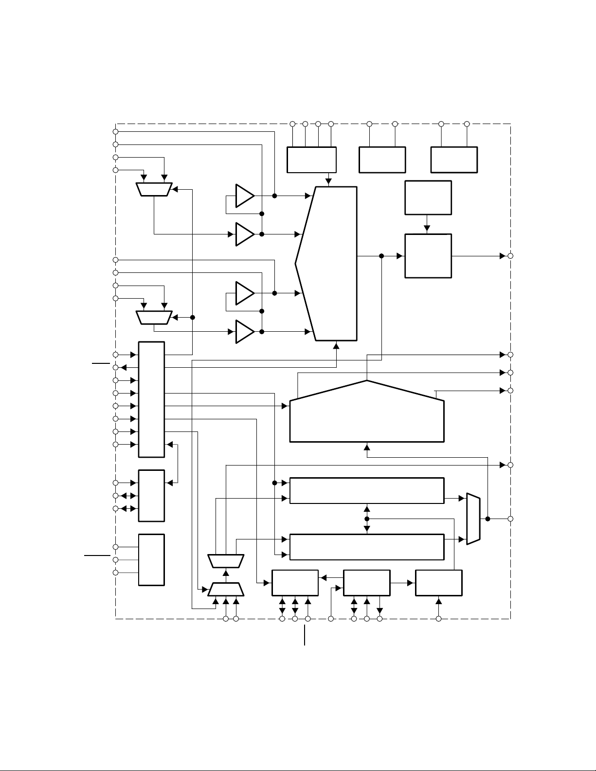
1.3 Functional Block Diagram
AINRP
AINRM
RINA
RINB
AINLP
AINLM
LINA
LINB
ALLPASS
INPA
GPI5
GPI4
GPI3
GPI2
GPI1
GPI0
Controller
L+R
SS(REF)
REFM
REFP
V
V
AV
Voltage
Reference
AINRP
AINRM
24-Bit
Stereo
ADC
AINLP
AINLM
RFILT
V
Stereo DAC
DD
AV
Analog
Supplies
24-Bit
SS
AV
Analog
Control
Register
Output
Format
Control
Logic
DD
DV
Digital
Supplies
SS
DV
SDOUT0
VCOM
AOUTL
AOUTR
L+R
SDOUT2
CS1
SDA
SCL
PWR_DN
RESET
TEST
C
2
I
Control
Control
32-Bit Audio Signal
L
R
SDIN2
SDIN1
SDATA
Control
SCLK/O
LRCLK/O
32-Bit Audio Signal
IFM/S
CLKSEL
Figure 1–1. TAS3004 Block Diagram
Processor
Processor
OSC/CLK
Select
MCLK
XTALI/
XTALO
MCLKO
SDOUT1
PLL
CAP_PLL
1–3
Page 12
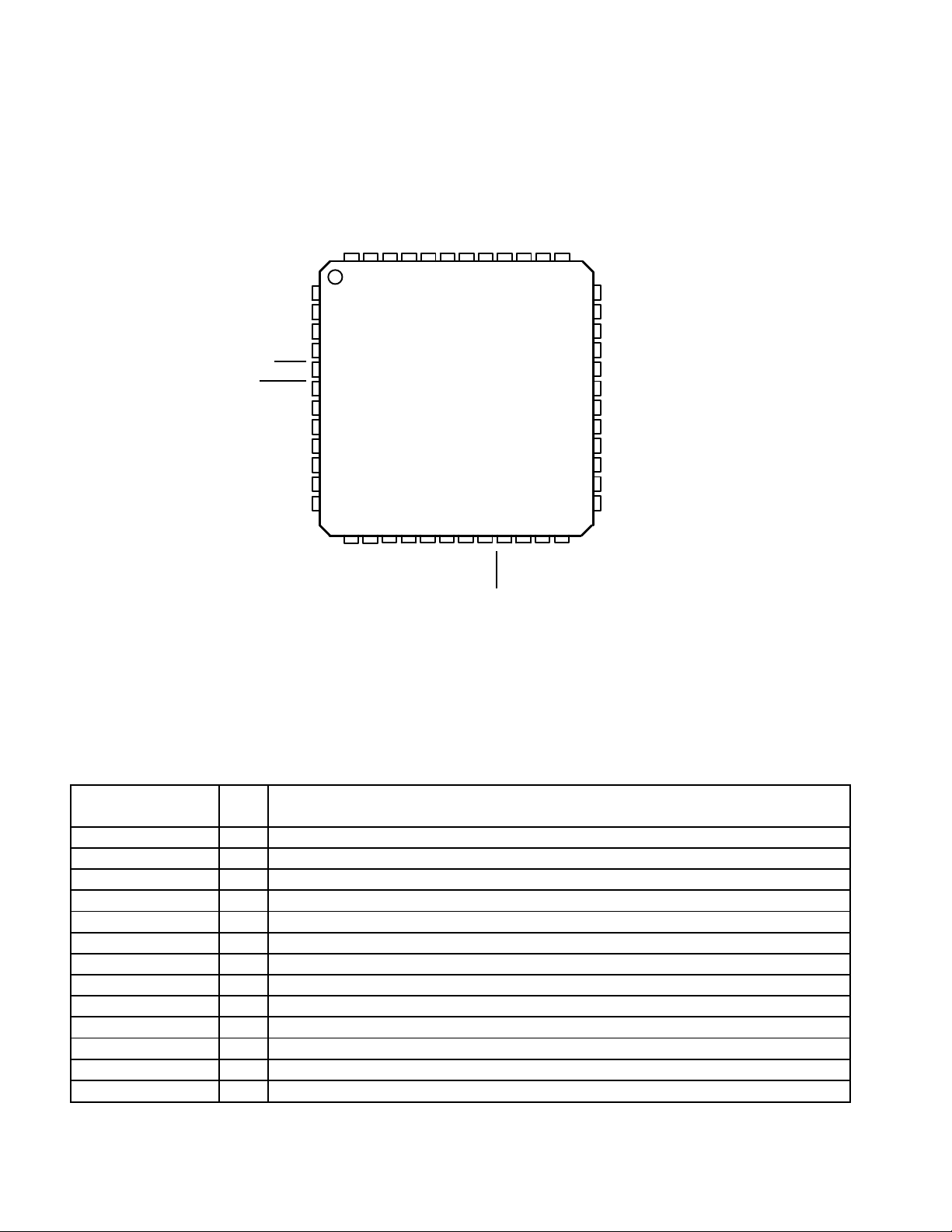
1.4 Terminal Assignments
LINB
AINLP
REFMVREFP
AINLM
V
PACKAGE
(TOP VIEW)
AINRM
AINRP
RINA
RINB
VCOM
AOUTL
AOUTR
V
RFILT
AV
SS(REF)
AV
RESET
PWR_DN
TEST
CAP_PLL
CLKSEL
MCLKO
1.5 Terminal Functions
LINA
SS
INPA
CS1
47 46 45 44 4348 42
1
2
3
4
5
6
7
8
9
10
11
12
14 15
13
XTALO
17 18 19 20
16
SCL
SDA
DD
DV
SS
DV
LRCLK/O
40 39 3841
22 23 24
21
IFM/S
SCLK/O
37
SDIN1
SDIN2
XTALI/MCLK
Figure 1–2. TAS3004 Terminal Assignments
NC
36
AV
35
NC
34
33
GPI5
32
GPI4
GPI3
31
GPI2
30
GPI1
29
GPI0
28
ALLPASS
27
SDOUT1
26
SDOUT0
25
SDOUT2
DD
Table 1–1. TAS3004 Terminal Functions
TERMINAL
NAME NO.
AINLM 46 I ADC left channel analog input (anti-alias capacitor)
AINLP 47 I ADC left channel analog input (anti-alias capacitor)
AINRM 43 I ADC right channel analog input (anti-alias capacitor)
AINRP 42 I ADC right channel analog input (anti-alias capacitor)
ALLPASS 27 I Logic high bypasses equalization filters
AOUTL 39 O Left channel analog output
AOUTR 37 O Right channel analog output
AV
DD
AV
SS
AV
SS(REF)
CAP_PLL 10 I Loop filter for internal phase-locked loop (PLL)
CLKSEL 11 I Logic low selects 256fS; logic high selects 512fS MCLK
CS1 7 I I2C address bit A0; low = 68h, high = 6Ah
1–4
I/O
35 I Analog power supply (3.3 V)
4 I Analog voltage ground
3 I Analog ground voltage reference
DESCRIPTION
Page 13

Table 1–1. TAS3004 Terminal Functions (Continued)
TERMINAL
NAME NO.
DV
DD
DV
SS
GPI0
GPI1
GPI2
GPI3
GPI4
GPI5
IFM/S 21 I Digital audio I/O control (low = input; high = output)
INPA 5 O Low when analog input A is selected (will sink 4 mA)
LINA 1 I Left channel analog input 1
LINB 48 I Left channel analog input 2
LRCLK/O 19 I/O Left/right clock input/output (output when IFM/S is high)
MCLKO 12 O MCLK output for slave devices
NC 34 No connection; Can be used as a printed circuit board routing channel
NC 36 No connection; Can be used as a printed circuit board routing channel
PWR_DN 8 I Logic high places the TAS3004 device in power-down mode
RESET 6 I Logic low resets the TAS3004 device to the initial state
RINA 40 I Right channel analog input 1
RINB 41 I Right channel analog input 2
SCL 15 I/O I2C clock connection
SCLK/O 20 I/O Shift (bit) clock input (output when IFM/S is high)
SDA 16 I/O I2C data connection
SDIN1 22 I Serial data input 1
SDIN2 23 I Serial data input 2
SDOUT1 26 O Serial data output (from internal audio processing)
SDOUT2 24 O Serial data output (a monaural mix of left and right, before processing)
SDOUT0 25 O Serial data output from ADC
TEST 9 I Reserved manufacturing test terminal; connect to DV
VCOM 38 O Digital-to-analog converter mid-rail supply (decouple with parallel combination of 10-µF and 0.1-µF
V
REFM
V
REFP
V
RFILT
XTALI/MCLK 13 I Crystal or external MCLK input
XTALO 14 I Crystal input (crystal is connected between terminals 13 and 14)
I/O
17 I Digital power supply (3.3 V)
18 I Digital ground
28
29
30
31
32
33
45 I ADC minus voltage reference
44 I ADC plus voltage reference
I Switch input terminals
capacitors)
2 O Voltage reference low pass filter
DESCRIPTION
SS
1–5
Page 14

1–6
Page 15

2 Audio Data Formats
2.1 Serial Interface Formats
The TAS3004 device works in master or slave mode.
In the master mode, terminal 21 (IFM/S
) is tied high. This activates the master clock (MCLK) circuitry. A crystal can
be connected across terminals 13 (XTALI/MCLK) and 14 (XTALO), or an external, TTL-compatible MCLK can be
connected to X TALI/MCLK. In that case, MCLK outputs from terminal 12 (MCLKO) with terminals 19 (LRCLK/O) and
20 (SCLK/O) becoming outputs to drive slave devices.
In the slave mode, IFM/S
is tied low. LRCLK/O and SCLK/O are inputs and the interface operates as a slave device
requiring externally supplied MCLK, LRCLK (left/right clock), and SCLK (shift clock) inputs. There are two options
for selecting the clock rates. If the 512f
of 512f
must be supplied. If the 256fS MCLK is selected, CLKSEL is tied low and an MCLK of 256fS must be supplied.
S
MCLK rate is selected, terminal 1 1 (CLKSEL) is tied high and an MCLK rate
S
In both cases, an LRCLK of 64SCLK must be supplied.
• MCLK and SCLK must be synchronous and their edges must be at least 3 ns apart.
• If the LRCLK phase changes more than 10MCLK, the codec automatically resets.
2
The TAS3004 device is compatible with 13 different serial interfaces. Available interface options are I
and left justified. Table 2–1 indicates how the 13 options are selected using the I
(MCR, I
Additionally, the 16-bit mode operates at 32f
2
C address x01h). All serial interface options at either 16, 18, 20, or 24 bits operate with SCLK at 64fS.
.
S
2
C bus and the main control register
S, right justified,
Table 2–1. Serial Interface Options
MODE MCR BIT (6) MCR BIT (5–4) MCR BIT (1–0)
0 0 00 00 16-bit, left justified, 32f
1 1 00 00 16-bit, left justified, 64f
2 1 01 00 16-bit, right justified, 64f
3 1 10 00 16-bit, I2S, 64f
4 1 00 01 18-bit, left justified, 64f
5 1 01 01 18-bit, right justified, 64f
6 1 10 01 18-bit, I2S, 64f
7 1 00 10 20-bit, left justified, 64f
8 1 01 10 20-bit, right justified, 64f
9 1 10 10 20-bit, I2S, 64f
10 1 00 11 24-bit, left justified, 64f
11 1 01 11 24-bit, right justified, 64f
12 1 10 11 24-bit, I2S, 64f
SDIN1, SDIN2, SDOUT1, SDOUT2, AND SDOUT0
S
S
S
S
SERIAL INTERFACE
S
S
S
S
S
S
S
S
S
Figure 2–1 through Figure 2–9 illustrate the relationship between the SCLK, LRCLK, and the serial data I/O for the
different interface protocols.
2–1
Page 16
2.2 ADC Digital Output Modes
ADC digital output mode (SDOUT0) has two operational modes, normal and monaural. In the normal mode, the
output of the ADC conforms to the output modes described in Sections 2.2.1 through 2.2.3. To enter the normal output
mode, bit 7 (ADM) in the analog control register must be cleared to 0. In the monaural output mode, the digital output
of the ADC conforms to the output modes described in Sections 2.3.1 through 2.3.6. To enter the monaural mode,
bit 7 (ADM) in the analog control register must be set to 1.
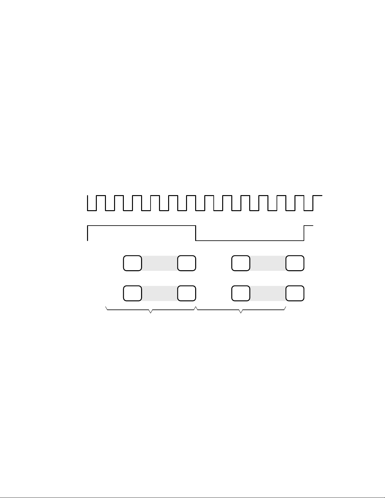
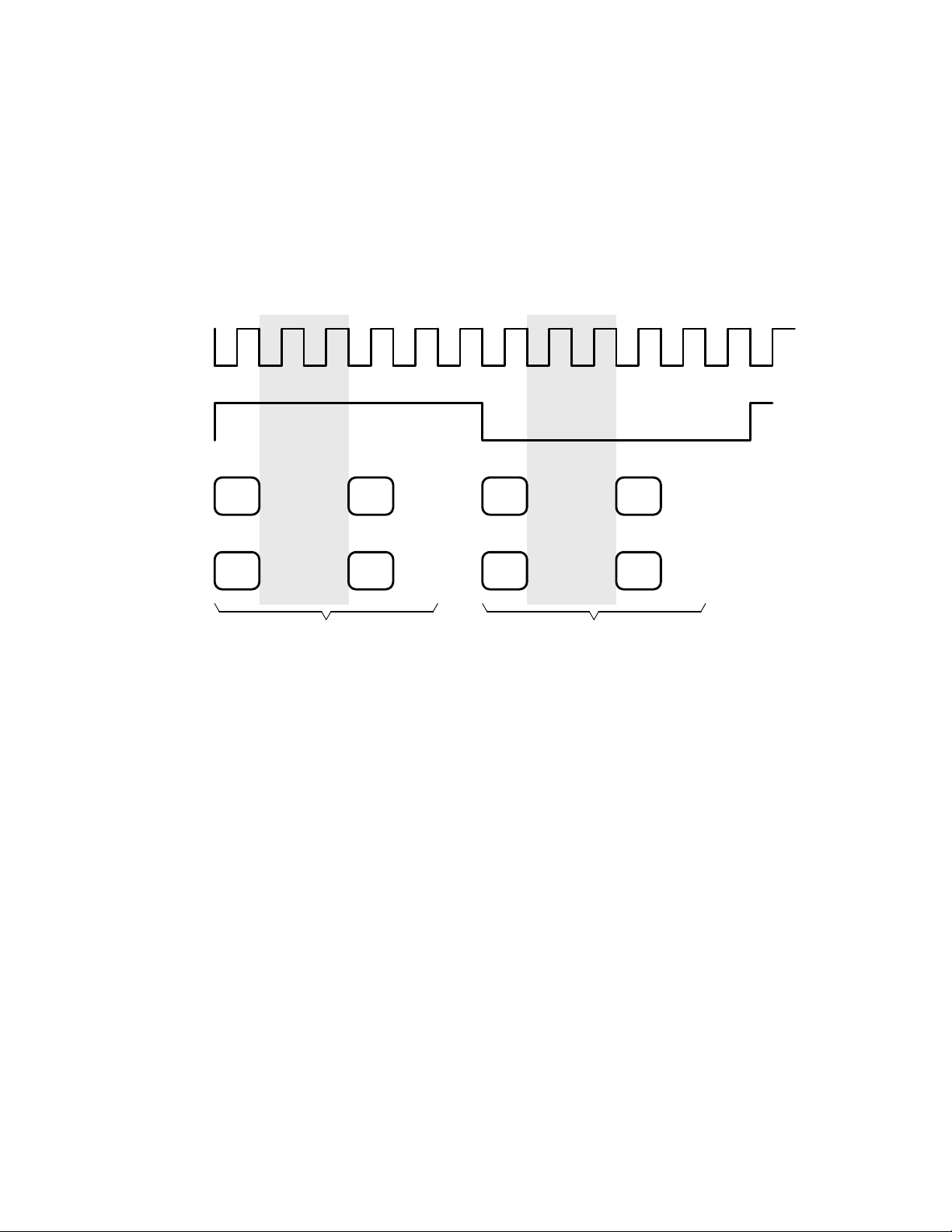
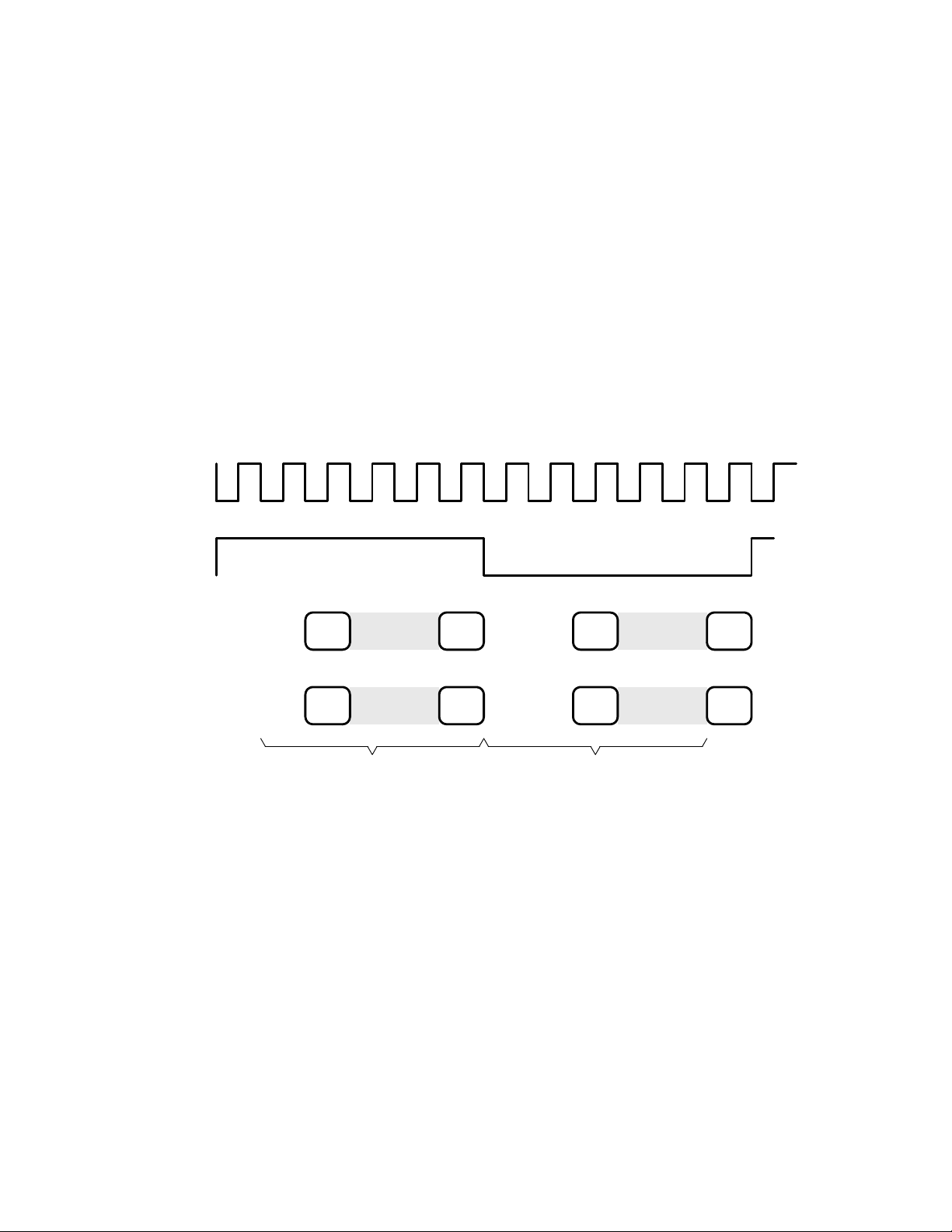
2.2.1 MSB First, Right-Justified Serial Interface Format—Normal Mode
The normal output mode for the MSB first, right-justified serial interface format is for 16, 18, 20, and 24 bits with bit 7
(ADM) in the analog control register cleared to 0. Figure 2–1 shows the following characteristics of this protocol:
• Left channel is transmitted when LRCLK is high.
• The SDIN(s) (recorded) data is justified to the trailing edge of the LRCLK.
• The SDOUT(s) MSB (playback) data is transmitted at the same time as LRCLK edge and captured at the
next rising edge of SCLK.
• If LRCLK phase changes by more than 10MCLK, the codec automatically resets.
SCLK
LRCLK = f
S
SDIN
SDOUT
Figure 2–1. MSB First, Right-Justified Serial Interface Format—Normal Mode
……
MSB LSB
MSB LSB
………… ……
…… ……
Left Channel Right Channel
MSB LSB
MSB LSB
……
……
2–2
Page 17
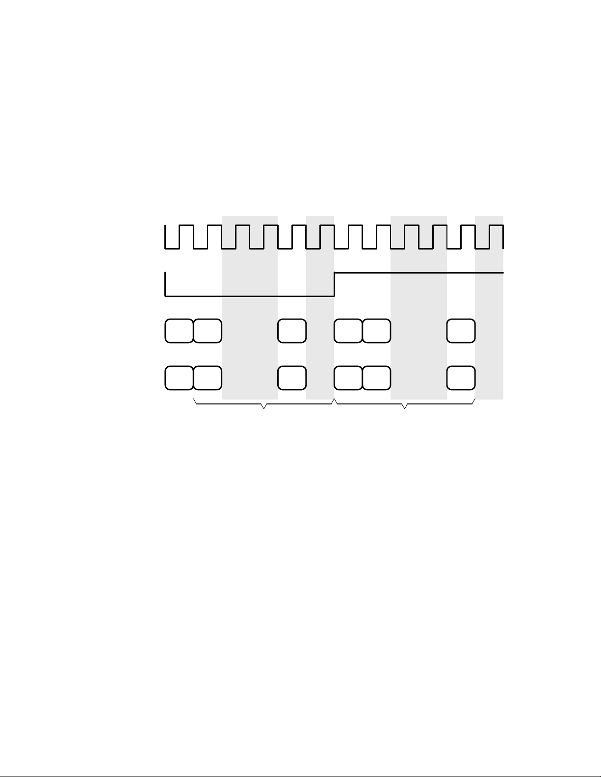
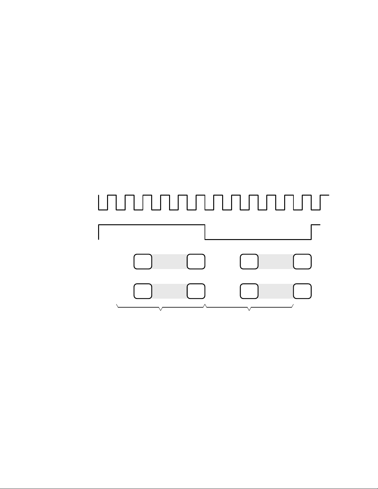
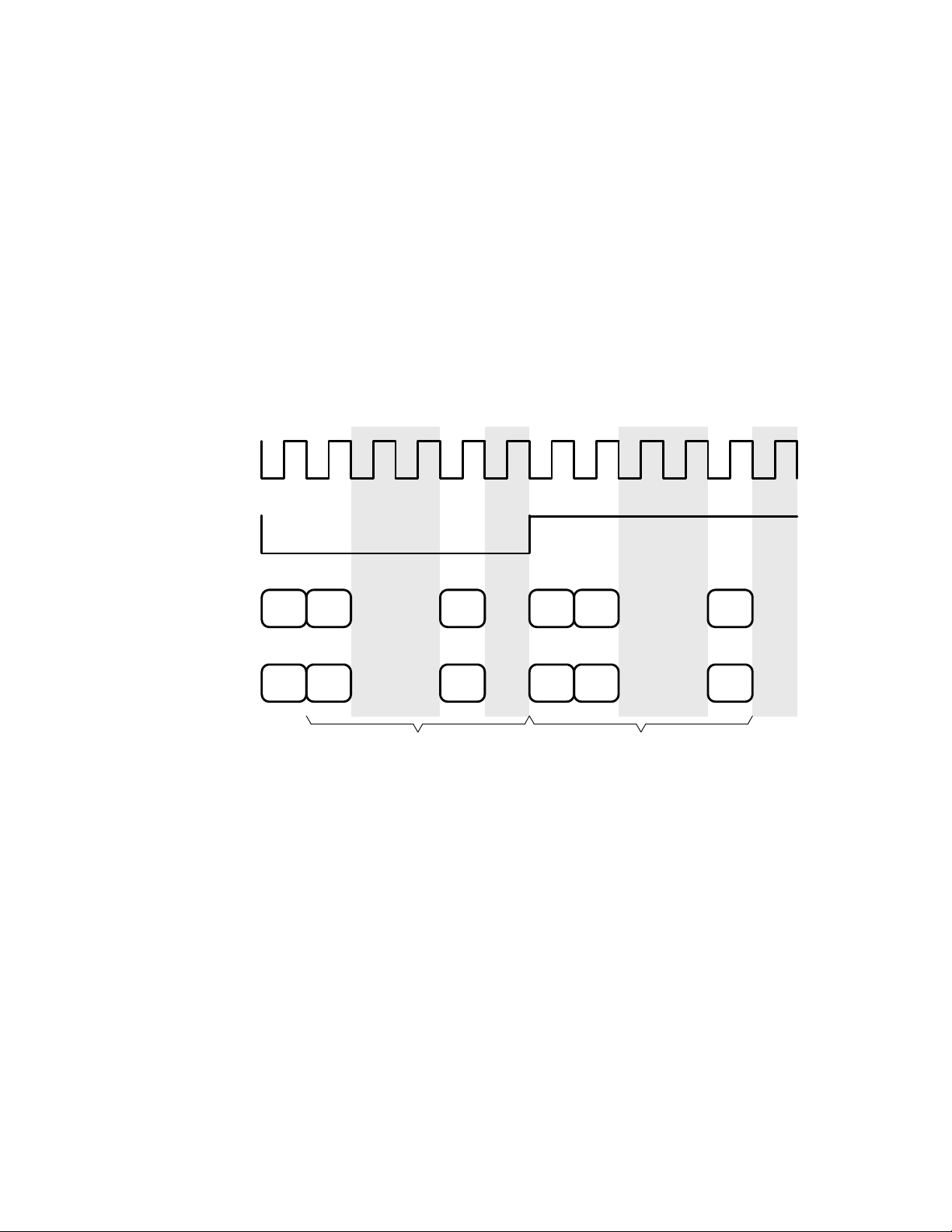
2.2.2 I2S Serial Interface Format—Normal Mode
The normal output mode for the I2S serial interface format is for 16, 18, 20, and 24 bits with bit 7 (ADM) in the analog
control register cleared to 0.
Figure 2–2 shows the following characteristics of this protocol:
• Left channel is transmitted when LRCLK is low.
• SDIN is sampled with the rising edge of SCLK.
• SDOUT is transmitted on the falling edge of SCLK.
• If LRCLK phase changes by more than 10MCLK, the codec automatically resets.
SCLK
LRCLK = f
SDIN
SDOUT
S
X LSB
MSB
X LSB
MSB
Figure 2–2. I2S Serial Interface Format—Normal Mode
……
……
Left Channel Right Channel
…
…
X LSB
MSB
X LSB
MSB
……
……
…
…
2–3
Page 18
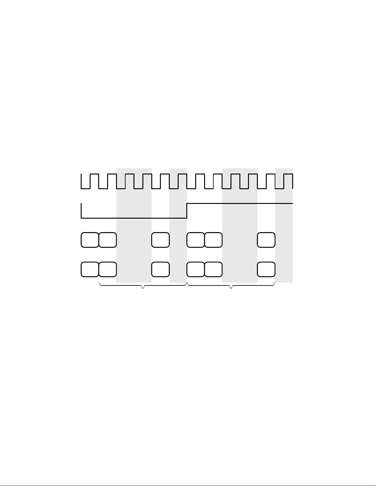
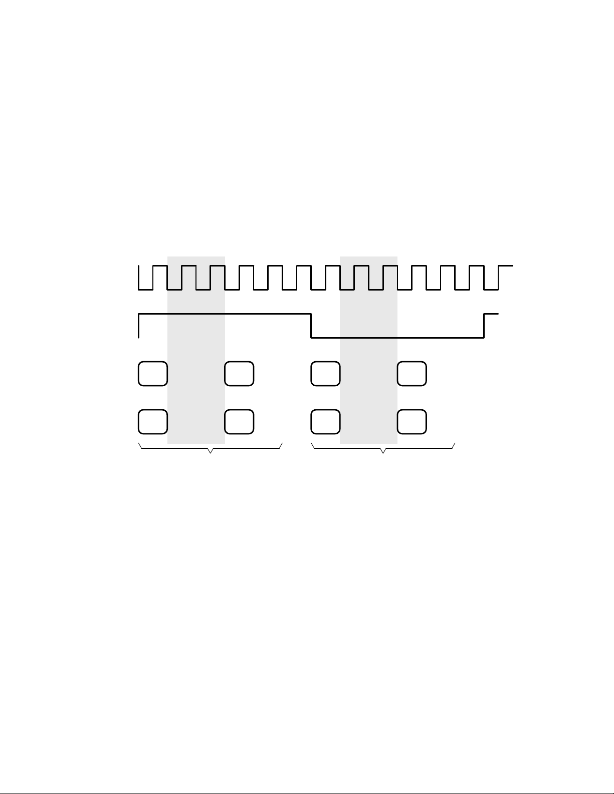
2.2.3 MSB Left-Justified Serial Interface Format—Normal Mode
The normal output mode for the MSB left-justified serial interface format is for 16, 18, 20, and 24 bits with bit 7 (ADM)
in the analog control register cleared to 0.
Figure 2–3 shows the following characteristics of this protocol:
• Left channel is transmitted when LRCLK is high.
• The SDIN data is justified to the leading edge of the LRCLK.
• The MSBs are transmitted at the same time as LRCLK edge and captured at the next rising edge of SCLK.
SCLK
LRCLK = f
SDIN
SDOUT
S
MSB LSB
MSB LSB
Figure 2–3. MSB Left-Justified Serial Interface Format—Normal Mode
……
……
Left Channel Right Channel
……
……
MSB LSB
MSB LSB
……
……
……
……
2.3 ADC Digital Output Mode—Monaural
For the monaural ADC digital output mode, bit 7 (ADM) is set to 1, and bit 6 (LRB) and bit 1 (INP) in the analog control
register (see Section 4.8, Analog Control Register Operation) control the operation of the monaural output mode. All
interface formats are for 16, 18, 20, and 24 bits.
2–4
Page 19
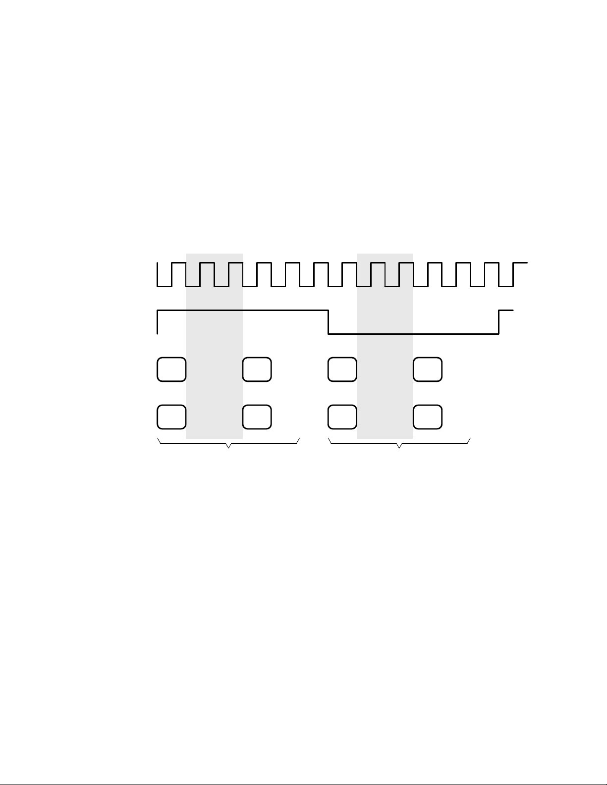
2.3.1 MSB First, Right-Justified Serial Interface Format—Monaural ADC Mode, B Left Input
Selected
The monaural output mode for the MSB first, right-justified serial interface format is for 16, 18, 20, and 24 bits with
the following bits in the analog control register set as shown:
• Bit 7 (ADM) is set to 1.
• Bit 6 (LRB) is cleared to 0.
• Bit 1 (INP) is set to 1.
Figure 2–4 shows the following characteristics of this protocol:
• Left channel is transmitted when LRCLK is either high or low.
• The SDIN(s) (recorded) data is justified to the trailing edge of the LRCLK.
• The SDOUT(s) MSB (playback) data is transmitted at the same time as LRCLK edge and captured at the
next rising edge of SCLK.
• If LRCLK phase changes by more than 10MCLK, the codec automatically resets.
SCLK
LRCLK = f
Figure 2–4. MSB First, Right-Justified Serial Interface Format—Monaural ADC Mode, B Left Input
SDIN
SDOUT0
S
……
MSB LSB
MSB LSB
………… ……
…… ……
Left Channel Left Channel
Selected
MSB LSB
MSB LSB
……
……
2–5
Page 20
2.3.2 I2S Serial Interface Format—Monaural ADC Mode, B Left Input Selected
The monaural output mode for the I2S serial interface format is for 16, 18, 20, and 24 bits with the following bits in
the analog control register set as shown:
• Bit 7 (ADM) is set to 1.
• Bit 6 (LRB) is cleared to 0.
• Bit 1 (INP) is set to 1.
Figure 2–5 shows the following characteristics of this protocol:
• Left channel is transmitted when LRCLK is either high or low.
• SDIN is sampled with the rising edge of SCLK.
• SDOUT is transmitted on the falling edge of SCLK.
• If LRCLK phase changes by more than 10MCLK, the codec automatically resets.
SCLK
LRCLK = f
S
X LSB
SDIN
SDOUT0
Figure 2–5. I2S Serial Interface Format—Monaural ADC Mode, B Left Input Selected
MSB
MSB
X LSB
……
……
Left Channel Left Channel
…
…
X LSB
MSB
X LSB
MSB
……
……
…
…
2–6
Page 21
2.3.3 MSB Left-Justified Serial Interface Format—Monaural ADC Mode, B Left Input Selected
The monaural output mode for the MSB left-justified serial interface format is for 16, 18, 20, and 24 bits with the
following bits in the analog control register set as shown:
• Bit 7 (ADM) is set to 1.
• Bit 6 (LRB) is cleared to 0.
• Bit 1 (INP) is set to 1.
Figure 2–6 shows the following characteristics of this protocol:
• Left channel is transmitted when LRCLK is either high or low.
• The SDIN data is justified to the leading edge of the LRCLK.
• The MSBs are transmitted at the same time as LRCLK edge and captured at the next rising edge of SCLK.
SCLK
LRCLK = f
Figure 2–6. MSB Left-Justified Serial Interface Format—Monaural ADC Mode, B Left Input Selected
SDIN
SDOUT0
S
MSB LSB
MSB LSB
……
……
Left Channel Left Channel
……
……
MSB LSB
MSB LSB
……
……
……
……
2–7
Page 22
2.3.4 MSB First, Right-Justified Serial Interface Format—Monaural ADC Mode, B Right Input
Selected
The monaural output mode for the MSB first, right-justified serial interface format is for 16, 18, 20, and 24 bits with
the following bits in the analog control register set as shown:
• Bit 7 (ADM) is set to 1.
• Bit 6 (LRB) is set to 1.
• Bit 1 (INP) is set to 1.
Figure 2–7 shows the following characteristics of this protocol:
• Right channel is transmitted when LRCLK is either high or low.
• The SDIN(s) (recorded) data is justified to the trailing edge of the LRCLK.
• The SDOUT(s) MSB (playback) data is transmitted at the same time as LRCLK edge and captured at the
next rising edge of SCLK.
• If LRCLK phase changes by more than 10MCLK, the codec automatically resets.
SCLK
LRCLK = f
Figure 2–7. MSB First, Right-Justified Serial Interface Format—Monaural ADC Mode, B Right Input
SDIN
SDOUT0
S
……
MSB LSB
MSB LSB
………… ……
…… ……
Right Channel
Selected
MSB LSB
MSB LSB
Right Channel
……
……
2–8
Page 23
2.3.5 I2S Serial Interface Format—Monaural ADC Mode, B Right Input Selected
The monaural output mode for the I2S serial interface format is for 16, 18, 20, and 24 bits with the following bits in
the analog control register set as shown:
• Bit 7 (ADM) is set to 1.
• Bit 6 (LRB) is set to 1.
• Bit 1 (INP) is set to 1.
Figure 2–8 shows the following characteristics of this protocol:
• Right channel is transmitted when LRCLK is either high or low.
• SDIN is sampled with the rising edge of SCLK.
• SDOUT is transmitted on the falling edge of SCLK.
• If LRCLK phase changes by more than 10MCLK, the codec automatically resets.
SCLK
LRCLK = f
Figure 2–8. I2S Serial Interface Format—Monaural ADC Mode, B Right Input Selected
SDIN
SDOUT0
S
X LSB
MSB
X LSB
MSB
……
……
X LSB
…
…
Right Channel Right Channel
MSB
X LSB
MSB
……
……
…
…
2–9
Page 24
2.3.6 MSB Left-Justified Serial Interface Format—Monaural ADC Mode, B Right Input Selected
The monaural output mode for the MSB left-justified serial interface format is for 16, 18, 20, and 24 bits with the
following bits in the analog control register set as shown:
• Bit 7 (ADM) is set to 1.
• Bit 6 (LRB) is set to 1.
• Bit 1 (INP) is set to 1.
Figure 2–9 shows the following characteristics of this protocol:
• Right channel is transmitted when LRCLK is either high or low.
• The SDIN data is justified to the leading edge of the LRCLK.
• The MSBs are transmitted at the same time as LRCLK edge and captured at the next rising edge of SCLK.
SCLK
LRCLK = f
Figure 2–9. MSB Left-Justified Serial Interface Format—Monaural ADC Mode, B Right Input Selected
SDIN
SDOUT0
S
MSB LSB
MSB LSB
……
……
Right Channel Right Channel
……
……
MSB LSB
MSB LSB
……
……
……
……
2–10
Page 25

2.4 Switching Characteristics
PARAMETER MIN TYP MAX UNIT
t
c(SCLK)
t
d(SLR)
t
d(SDOUT)
t
su(SDIN)
t
h(SDIN)
LRCLK 32 44.1 48 kHz
NOTE 1: Maximum of 50-pF external load on SDOUT.
SCLK frequency 3.072 MHz
SCLK rising to LRCLK edge 20 ns
SDOUT valid from SCLK falling (see Note 1) (1/256fS) + 10 ns
SDIN setup before SCLK rising edge 20 ns
SDIN hold after SCLK rising edge 100 ns
Duty cycle 50 %
t
SCLK
LRCLK
c(SCLK)
t
d(SLR)
t
f(SCLK)
t
r(SCLK)
t
h(SDIN)
t
d(SLR)
SDOUT1
SDOUT2
SDOUT0
SDIN1
SDIN2
t
su(SDIN)
t
d(SDOUT)
Figure 2–10. For Right-/Left-Justified, I2S, and Left-/Left-Justified Serial Protocols
2–11
Page 26

2–12
Page 27

3 Analog Input/Output
The TAS3004 device contains a stereo 24-bit ADC with two single-ended inputs per channel. Selection of the A or
B analog input is accomplished by setting a bit in the analog control register (ACR) by an I
2
C command. Additionally,
the TAS3004 device has a stereo 24-bit digital-to-analog converter (DAC).
3.1 Analog Input
Figure 3–1 shows the technique and components required for analog input to the TAS3004 device. The maximum
input signal must not exceed 0.7 V
20 Hz to 20 kHz at a sampling frequency of 48 kHz without alias frequency problems.
0.47 µF
1
1
0.47 µF
0.47 µF
1
1
0.47 µF
. Selection of the above component values gives a frequency response from
rms
2
1200 pF
2
1200 pF
AINRP
AINRM
RINA
RINB
AINLP
AINLM
LINA
LINB
Voltage
Reference
AINRP
AINRM
24-Bit
Stereo
ADC
AINLP
1 Analog Inputs – Use 0.47 µF for 20-Hz Cutoff
2
Anti-Alias Capacitors for fS = 48 kHz
3 Tie unused analog inputs to analog ground through 0.1-µF capacitors.
Figure 3–1. Analog Input to the TAS3004 Device
3.2 Analog Output
3.2.1 Analog Output
The full scale analog output from the TAS3004 device is 0.7 V
1.5 Vdc. VCOM must be decoupled with the network as shown in Figure 3–2.
. It is referenced to VCOM which is approximately
rms
AINLM
Input Select Command
From Internal Controller
3–1
Page 28

AOUTR
(Adjust Capacitors for Desired
Analog Output
Low Frequency Response)
24-Bit
DAC
VCOM
10 µF
AOUTL
+
0.1 µF
AGND
Figure 3–2. VCOM Decoupling Network
3.2.2 Analog Output With Gain
Since the analog output from the TAS3004 device is 0.7 V
amplifier. The circuit shown in Figure 3–3 boosts the output level to 1 V
improved signal-to-noise ratio (SNR). Since this circuit lowers the noise floor, THD + N is improved also.
AOUTR
C1
24-Bit
DAC
VCOM
+
10 µF
C3
0.1 µF
, the output level can be increased by using an external
rms
–
+
(when it has a gain of 1.414) and provides
rms
C4
Analog Output
(Adjust Capacitors for Desired
Low Frequency Response)
TLV2362
or Equilvalent
3–2
C1 = C2 = C
C4 = C
5
3
AOUTL
C2
AGND
+5 Op Amp/2
+5 Op Amp/2
C5C5
–
+
TLV2362
or Equilvalent
Figure 3–3. Analog Output With External Amplifier
Page 29

3.2.3 Reference Voltage Filter
Figure 3–4 shows the TAS3004 reference voltage filter.
0.1 µF
15 µF
+
0.1 µF
4 23 45
SS
AV
SS(REF)
AV
RFILT
V
REFM
V
1 µF
0.1 µF
REFP
+
44V
TAS3004
Figure 3–4. TAS3004 Reference Voltage Filter
3–3
Page 30

3–4
Page 31

4 Audio Control/Enhancement Functions
4.1 Soft Volume Update
The TAS3004 device implements a TI proprietary soft volume update. This feature allows a smooth and
pleasant-sounding change from one volume level to another over the entire range of volume control (18 dB to mute).
2
The volume is adjustable by downloading a 4.16 gain coefficient through the I
coefficients converted into dB for the range of –70 dB to 18 dB with 0.5-dB step resolution.
Right and left channel volumes can be unganged and set to different values. This feature implements a balance
control.
Volume is changed by writing the desired value into the volume control registers. This is done by asserting the GPI
terminals for volume-up or volume-down for a limited range of volume control. Alternately, volume control settings
can be sent to the TAS3004 device over the I
2
C bus.
4.2 Software Soft Mute
Mute is implemented by loading all zeros in the volume control register. This causes the volume to ramp down over
a duration of 2048f
Soft mute can be enabled by either asserting the mute GPI terminal or sending a mute command over the I
samples to a final output of 0 (– infinity dB).
S
4.3 Input Mixer Control
C interface. Table A –5 lists the 4.16
2
C bus.
The TAS3004 device is capable of mixing and multiplexing three channels of serial audio data. The mixing is
controlled through three mixer control registers. This is accomplished by loading values into the corresponding bytes
of the mixer left gain (07h) and mixer right gain (08h) control registers.
The values loaded into these registers are in 4.20 format—4 bits for the integer and 20 bits for the fractional part.
T able A–8 lists the 4.20 numbers converted into dB for the range of –70 dB to 18 dB, although any positive 4.20
number may be used.
To mute any of the channels, 0s are loaded into the respective mixer control register.
Mixer controls are updated instantly and can cause audible artifacts for large changes in setting when updated
dynamically outside of the fast load mode; therefore, it is desirable to use fast load in conjunction with the soft-volume
mode.
SDIN1, SDIN2, and the ADC output can be mixed with a user-selectable gain for each channel. The gain control
registers are represented in 4.20 format.
4–1
Page 32

SDIN1_L
Left Channel Mix Coefficients
I2C Register Address 08h
SDIN1 ^ SDIN2 ^ ADC
= (3) 24-Bit Left Mix Coefficient
SDIN2_L
ADC_L
SDIN1_R
SDIN2_R
ADC_R
L_SUM
R_SUM
Right Channel Mix Coefficients
I2C Register Address 07h
7 Biquad
Filters
7 Biquad
Filters
1/2
1/2
Tone
Tone
Soft
Volume
DRCE
Soft
Volume
DRCE
L + R_SUM
SDIN1 ^ SDIN2 ^ ADC
= (3) 24-Bit Right Mix Coefficient
SDOUT1
SDOUT2
Figure 4–1. TAS3004 Mix Function
4.4 Mono Mixer Control
The TAS3004 device contains a second mixer that performs the function of mixing left and right channel digital audio
data from the input mixer in order to derive a monaural channel. This mixer has a fixed gain of –6 dB so that full scale
inputs on L_sum and R_sum do not produce clipping on the resulting L+R_sum.
The output of this mixer is present on terminal 24 (SDOUT2) and is generally used for a digitally-mixed subwoofer
or center channel application.
4.5 Treble Control
The treble gain level may be adjusted within the range of 15 dB to –15 dB with 0.5-dB step resolution. The level
changes are accomplished by downloading treble codes (shown in Appendix A) into the treble gain register.
Alternately, a limited range of treble control is available by asserting the GPI terminals.
The treble control has a corner frequency of 6 kHz at a 48-kHz sample rate.
The gain values for treble control can be found in Section A.3.
4–2
Page 33

4.6 Bass Control
The bass gain level can be adjusted within the range of 15 dB to –15 dB with 0.5-dB step resolution. The level changes
are accomplished by downloading bass codes (shown in Appendix A) into the bass frequency control register.
Alternately, a limited range of bass control is available by asserting the GPI terminals.
Bass control is a shelf filter with a corner frequency of 250 Hz at a 48-kHz sample rate.
The gain values for bass control can be found in Section A.4.
4.7 De-Emphasis (DM)
De-emphasis is implemented in the DAC and is software controlled. De-emphasis is valid at 44.1 kHz and 48 kHz.
2
To enable de-emphasis, values are written into the analog control register via the I
analog control register operation.
Figure 4–2 illustrates the frequency response of the de-emphasis mode.
C command. See Section 4.8 for
Response (dB)
De-Emphasis
3.18
(50 µs)
Frequency (kHz)
10.6
(15 µs)
Figure 4–2. De-Emphasis Mode Frequency Response
4–3
Page 34

4.8 Analog Control Register Operation
The analog control register (ACR) allows control of de-emphasis, selection of the analog input channel to the ADC,
and analog power down.
2
C master is required to write the appropriate command into the ACR. The ACR subaddress is 0x40.
An I
Bit 7 6 5 4 3 2 1 0
Type R/W R/W R/W R/W R/W R/W R/W R/W
Default 0 0 0 0 0 0 0 0
Table 4–1. Analog Control Register Description
BIT FIELD NAME TYPE DESCRIPTION
7 ADM R/W ADC output mode.
0 = Normal operation
1 = A inputs are normal; B inputs are monaural.
6 LRB R/W Selects left or right B input for monaural output.
0 = B left input selected for monaural ADC output when bit 7 (ADM) is set to 1
1 = B right input selected for monaural ADC output when bit 7 (ADM) is set to 1.
5–4 RSVD R/W Reserved. Bits 5 and 4 return 0s when read.
3–2 DM(1–0) R/W De-emphasis control.
00 = De-emphasis off (initial condition after reset)
01 = 48 kHz sample rate de-emphasis selected
10 = 44.1 kHz sample rate de-emphasis selected
11 = Reserved
1 INP R/W Analog input select.
0 = LINA and RINA selected (initial condition after reset)
1 = LINB and RINB selected
0 APD R/W Analog powerdown.
0 = Normal operation (initial condition after reset)
1 = Powerdown
.
4–4
Page 35

4.9 Dynamic Loudness Contour
The necessity for applying loudness compensation to playback systems to compensate for the fact that the ear
perceives bass and treble less audibly at low levels than at high ones has been established with the first data
published by Fletcher and Munson in 1933.
There are ma n y equal-loudness contours in publication, like Steven’s contours, Robinson and Dadson contours even
reached the acceptance level of ISO recommendation.
The TAS3004 device has a simplified loudness contour algorithm that diminishes the effect of weak bass at low
listening levels. Since contour has volume level dependency, the user must define the relation between the gain of
the contour circuit and the volume level.
Figure 4–3 is a block diagram of this circuit.
Volume
Biquad Gain
Figure 4–3. Block Diagram
2
The loudness contour is activated by sending an activation command via I
contour gain command can be sent by an external device to provide tracking with the system’s volume control.
C from an external device. Optionally, a
4.9.1 Loudness Biquads
Loudness biquad filters for the left and right channels are independently programmable via I2C. Their subaddresses
are 0x21 and 0x22, respectively . The digital filters are written as five 24-bit (4.20) hex coefficients for each channel.
4.9.2 Loudness Gain
Loudness gain values for the left and right channels are independently programmable via I2C. Their subaddresses
are 0x23 and 0x24, respectively. The gain values are written as one 4.20 hex coefficient for each channel.
4.9.3 Loudness Contour Operation
When the frequency of the loudness contour is determined, a digital filter must be developed. Then, the gain of the
filter is determined. These values are placed in the storage area of the system controller (microcontroller) and sent
to the TAS3004 device when it is desired to activate the loudness contour.
If it is necessary to change the frequency or gain of the contour, new gain and filter coefficients are sent by the system
controller. This function is performed normally when the volume control is changed (that is, more volume, less
contour). The gain of the loudness contour filter then tracks the volume control.
The loudness contour biquad filters are provided in addition to the seven equalization biquad filters.
See Section A.6 for programming instructions.
4–5
Page 36

4.10 Dynamic Range Compression/Expansion
The TAS3004 device provides the user with the ability to manage the dynamic range of the audio system. The DRCE
receives data, and affects scaling after the volume/loudness block. As shown in Figure 4–4, the DRCE is applied after
the volume/loudness control block as a DRCE scale factor. The DRCE must be adjusted such that the signal does
not reach the hard limit value. However, if the signal does reach the maximum digital value, the saturation logic serves
as a hard limiter that does not allow the signal to extend beyond the available range.
Loudness
(Left Channel Mixer)
SDIN1_L
LEFT_SUM
SDIN2_L
ANALOGIN_L
(Parametric
Equalization)
(7)
2nd Order
IIR Filters
(Tone)
Bass/
Treble
Soft
Volume/
(DRCE Scaling)
Saturation
Logic
LEFT_OUT
(Analog in From ADC)
ANALOGIN_R
SDIN1_R
SDIN2_R
(Right Channel Mixer)
RIGHT_SUM
(7)
2nd Order
IIR Filters
(Parametric
Equalization)
Bass/
Treble
(Tone)
Dynamic
Range
Control
Soft
Volume/
Loudness
(DRCE Scaling)
Saturation
Logic
RIGHT_OUT
Figure 4–4. TAS3004 Digital Signal Processing Block Diagram
The DRCE instruction consists of eight bytes that must be sent each time in the order shown in the example code
of Table A–9. Each instruction downloaded must be eight bytes. If only one byte is changed, all eight bytes must be
transmitted. The first two bytes remain the same for every instruction, however the last six bytes can be programmed
using hexadecimal values from the corresponding tables referred to in Section A.7.
With high compression ratios and fast attack times available, this function is suited for a commercial killer in a
television set application.
4.11 AllPass Function
This function is enabled by setting terminal 27 (ALLP ASS) on the TAS3004 device to 1. When asserted, the internal
equalization filters are set into AllPass (flat) mode. When this terminal is reset to 0, the equalization filters are returned
to the equalization that was in use before the terminal was asserted.
In AllPass mode, the bass and treble controls are still functional.
This function is frequently used for headphones. When the headphone plug is inserted into its jack, a switched contact
in the jack enables the AllPass function.
The AllPass function also can be activated by writing a 1 to bit 2 of the analog control register.
4–6
Page 37

4.12 Main Control Register 2 (43h)
The TAS3004 device contains two main control registers: main control register 1 (MCR1) and main control register 2
(MCR2). The MCR2 contains the bits associated with the AllPass function and the download of bass and treble control
information, and it is accessed via I
MCR2 (43h)
Bit b7 b6 b5 b4 b3 b2 b1 b0
Type R/W R R R R R R/W R
Default 0 0 0 x x x 0 0
BIT TYPE DESCRIPTION
b7 R/W 0 = Normal operation (initial condition after reset)
1 = Download bass and treble
b6–b5 R Reserved. Bits b6 and b5 return 0s when read.
b4–b2 R Undefined.
b1 R/W 0 = Normal operation (initial condition after reset)
1 = AllPass mode (bass and treble are still functional)
b0 R Reserved. Bit b0 returns 0 when read.
2
C with the address 43h.
Table 4–2. Main Control Register 2 Description
4–7
Page 38

4–8
Page 39

5 Filter Processor
5.1 Biquad Block
The biquad block consists of seven digital biquad filters per channel organized in a cascade structure, as shown in
Figure 5–1. Each of these biquad filters has five downloadable 24-bit (4.20) coefficients. Each stereo channel has
independent coefficients.
Biquad 2 ...Biquad 1 Biquad N
Figure 5–1. Biquad Cascade Configuration
5.1.1 Filter Coefficients
The filter coefficients for the TAS3004 device are downloaded through the I2C port and loaded into the biquad memory
space. Each biquad filter memory space has an independent address. Digital audio data coming into the device is
processed by the biquad block and then converted into analog waveforms by the DAC. Alternately, filters can be
loaded by asserting terminals on the GPI port.
5.1.2 Biquad Structure
The biquad structure that is used for the parametric equalization filters is as follows:
H(z) +
b0) b1z*1) b2z
a0) a1z*1) a2z
NOTE: a0 is fixed at value 1 and is not downloadable.
The coefficients for these filters are represented in 4.20 format—4 bits for the integer part and 20 bits for the fractional
part. In order to transmit them over I
of byte 2 is the integer part, and the second nibble of byte 2, byte 1, and byte 0 are the fractional parts.
The filters can be designed using the automatic loudspeaker equalization program (ALE) or a script running under
MatLab named Filtermaker. Both of these tools are available from Texas Instruments.
*2
*2
2
C, it is necessary to separate each coefficient into three bytes. The upper 4 bits
(1)
5–1
Page 40

5–2
Page 41

6I2C Serial Control Interface
6.1 Introduction
Control parameters for the TAS3004 device can be loaded from an I2C serial EPROM by using the T AS3004 master
interface mode. If no EPROM is found, the TAS3004 device becomes a slave device and loads from another I
2
master interface. Information loaded into the TAS3004 registers is defined in Appendix A.
2
C bus uses terminals 16 (SDA for data) and 15 (SCL for clock) to communicate between integrated circuits in
The I
a system. These devices can be addressed by sending a unique 7-bit slave address plus R/W
bit (1 byte). All
compatible devices share the same terminals via a bidirectional bus using a wired-AND connection. An external
pullup resistor must be used to set the high level on the bus. The TAS3004 device operates in standard mode up to
100 kbps with as many devices on the bus as desired up to the capacitance load limit of 400 pF.
Furthermore, the TAS3004 device supports a subset of the SMBus protocol. When it is attached to the SMBUS, then
byte, word, and block transfers are supported. The SMBus NAK function is not supported and care must be taken
with the sequence of the instructions sent to the TAS3004 device.
Additionally, the TAS3004 device operates in either master or slave mode; therefore, at least one device connected
to the I
2
C bus must operate in master mode.
6.2 I2C Protocol
The bus standard uses transitions on SDA while the clock is high to indicate start and stop conditions. A high-to-low
transition on SDA indicates a start and a low-to-high transition indicates a stop. Normal data bit transitions must occur
within the low time of the clock period. Figure 6–1 shows these conditions. These start and stop conditions for the
2
I
C bus are required by standard protocol to be generated by the master. The master must also generate the 7-bit
slave address and the read/write (R/W
acknowledge condition. The slave holds SDA low during acknowledge clock period to indicate an acknowledgment.
When this occurs, the master transmits the next byte of the sequence.
) bit to open communication with another device and then wait for an
C
After each 8-bit word, an acknowledgment must be transmitted by the receiving device. There is no limit on the
number of bytes that can be transmitted between start and stop conditions. When the last word transfers, the master
generates a stop condition to release the bus. Figure 6–1 shows a generic data transfer sequence.
SDA
SCL
Start
7-Bit
Slave Address
R/
W
0
167
8-Bit Register Data
A
for Address (N)
0
167
8-Bit Register Data
A
for Address (N)
0
167
8-Bit Register Data
A
for Address (N+1)
A
0
167
Stop
Figure 6–1. Typical I2C Data Transfer Sequence
6–1
Page 42

Table 6–1 lists the definitions used by the I2C protocol.
2
Table 6–1. I
DEFINITION DESCRIPTION
Transmitter The device that sends data
Receiver The device that receives data
Master The device that initiates a transfer, generates clock signals, and terminates the transfer
Slave The device addressed by the master
Multimaster More than one master can attempt to control the bus at the same time without corrupting the message.
Arbitration Procedure to ensure the message is not corrupted when two masters attempt to control the bus.
Synchronization Procedure to synchronize the clock signals of two or more devices
C Protocol Definitions
6.3 Operation
The 7-bit address for the TAS3004 device is 0 11010X R/W where X is a programmable address bit, set by terminal 7
(CS1). Combining CS1 and the R/W
and two write). These two addresses are licensed I
devices. In addition to the 7-bit device address, subaddresses direct communication to the proper memory location
within the device. A complete table of subaddresses and control registers is provided in Appendix A. For example,
to change bass to 10-dB gain, Section 6.3.1 shows the data that is written to the I
I2C ADDRESS BYTE A6–A1 CS1 (A0) R/W
0x68 011010 0 0
0x69 011010 0 1
0x6A 011010 1 0
0x6B 011010 1 1
bit, the TAS3004 device can respond to four different I2C addresses (two read
2
C addresses that do not conflict with other licensed I2C audio
2
C port:
2
Table 6–2. I
C Address Byte Table
6.3.1 Write Cycle Example
Start Slave Address R/W A Subaddress A Data A Stop
FUNCTION DESCRIPTION
Start Start condition as defined in I2C
Slave address 0110100 (CS1 = 0)
R/W 0 (write)
A Acknowledgement as defined in I2C (slave)
Subaddress 00000110 (see Appendix A)
Data 00011100 (see Appendix A)
Stop Stop condition as defined in I2C
NOTE: Table is for serial data (SDA); serial clock (SCL) is not shown but conditions apply as well.
Whenever writing to a subaddress, the correct number of data bytes must follow in order to complete the write cycle.
For example, if the volume control register with subaddress 04 (hex) is written to, six bytes of data must follow;
otherwise, the cycle is incomplete and errors occur.
6–2
Page 43

6.3.2 TAS3004 I2C Readback Example
The T AS3004 will save in a Stack or First-In First-Out (FIFO) buf fer the last 7 bytes that were sent to it. When an I2C
read command is sent to the device (LSB=high), it answers by popping the first byte off the stack. The TAS3004 will
then expect either a SendAck command or an I
the host then the TAS3004 will pop another byte off the stack. If an I
transaction. The proper sequence for reading is described as follows:
I2C Start
Send I2C address byte with read Bit Set to 1 (LSB set equal to 1)
receive Byte 0
Send Ack
receive Byte 1
Send Ack
receive Byte 2
Send Ack
receive Byte 3
Send Ack
receive Byte 4
Send Ack
receive Byte 5
Send Ack
receive Byte 6 (if you send an ACK after Byte 6 it will lock up the TAS3004)
I2C Stop
2
C Stop command from the host. If a SendAck command is sent from
2
C Stop is sent then the TAS3004 will end this
Where:
2
C Start is a valid I2C Start Command
• I
• Receive Byte is a valid I
• SendAck is a avalid I
2
C Stop is a valid I2C Stop Command
• I
NOTES: 1. The TAS3004 will appear to be locked up, if a SendACK is issued after the last byte read. It is required to send an I2C Stop Condition
after the last byte and not a SendACK.
2. The I2Cstart and I2Cstop commands are the same for both I2C read and I2C write.
2
C Command which reads a byte from the TAS3004.
2
C Command that informs the TAS3004 that a byte has been read.
6.3.3 I2C Wait States
The TAS3004 device performs interpolation algorithms for its volume and tone controls. If a volume or tone change
is sent to the part via I
state to occur. This wait state lasts from 41 ms to 231 ms, depending on the system clock rate, the command sent,
and, in the case of bass or treble, the amount of the change.
Secondly, if a long series of commands are sent to the TAS3004 device, it may occasionally create a short wait state
on the order of 150 µs to 300 µs while it loads and processes the commands.
When a sample rate of 32 kHz is used, longer wait states can occur, occasionally up to 15 ms.
The preferred way to take care of wait states is to use an I
state period, it stops sending data over I
be implemented in the system software to ensure that the controller is not trying to send more data while the TAS3004
device is busy . Sending I
then be reset.
2
C, the command sent after the volume or tone (bass and treble) change causes an I2C wait
2
2
C. If this function is not available on the system controller, fixed delays can
2
C data while the TAS3004 device is busy causes errors and locks up the device, which must
C controller that recognizes wait states. During the wait
6–3
Page 44

Table 6–3 gives typical values of the wait states that can be expected with the various functions of the part:
2
Table 6–3. I
SYSTEM SAMPLING FREQUENCY
32 kHz 44.1 kHz 48 kHz
Volume 62 ms 49 ms 41 ms Not dependent on size of change
Bass 231 ms 167 ms 153 ms 0 to –18 dB, –1 dB = 0.055 T @ f
Treble 231 ms 167 ms 153 ms 0 to –18 dB, –1 dB = 0.055 T @ f
DRC On 300 µs 300 µs 300 µs
Mixer None None None
Loudness None None None
Equalization 15 ms 190 µs 300 µs Can occur with each filter
C Wait States
Comment
S
S
6.4 SMBus Operation
The TAS3004 device supports a subset of the SMBus protocol. With proper programming techniques, it is possible
to use the SMBus to set up the TAS3004 device.
6.4.1 Block Write Protocol
The TAS3004 device supports the block write protocol that allows up to 32 bytes to be sent as a block. To send a
command using this format, the most significant bit (MSB) of the TAS3004 subaddress must be set high and the
subaddress (also with MSB set high) must be programmed into the SMBus command byte. This operation signals
the TAS3004 device to realize that the next byte is the SMBus byte count byte. The next byte after the byte count is
then entered into the device as the first byte of data.
SMBus
Command Byte
68h 8rh xx dd dd dd
TAS3004
Address
Subaddress
(r = subaddress)
Byte Count
(Don’t Care)
Data Data Data
6.4.2 Write Byte Protocol
The TAS3004 device also supports the SMBus write byte protocol. Writing to the main control register (MCR), bass,
and treble registers require using the byte write protocol. To send a command using this format, the most significant
bit (MSB) of the TAS3004 subaddress must be set high and the subaddress (also with MSB set high) must be
programmed into the SMBus command byte. The next byte after the command byte is then entered into the device
as the first byte of data.
SMBus
Command Byte
68h
TAS3004
Address
8rh dd
Subaddress
(r = subaddress)
Data
6–4
Page 45

6.4.3 Wait States
If separate I2C/SMBus commands are sent too frequently, the TAS3004 device can generate a bus wait state. This
happens when the device is busy while performing smoothing operations and changing volume, bass, and treble.
The wait occurs after the bus acknowledge on the first data byte and can exceed the maximum allowable time allowed
according to the SMBus specification (worst case 200 ms).
The following is a possible bus wait state scenario:
CODE Start 68 84 06 01 00 00 01 00 00 Stop
ACTUAL Start 68 84 06 01 Wait
†
If the master does not recognize bus waiting or if the master times out on a long wait, the master must not send consecutive I2C/SMBus commands
without a time interval of 200 ms between transactions.
†
00 00 01 00 00 Stop
6.4.4 TAS3004 SMBus Readback
The TAS3004 device supports a subset of SMBus readback. When an SMBus read command is sent to the device
(LSB = high), it answers with the subaddress and the last six bytes written.
SMBus
Command
Byte
SENT
RECEIVED Start 07h aah ddh ddh ddh ddh ddh ddh Stop
Start 69h xxh 07h Stop
Byte
Count
Byte
Count
Where:
xxh = Command byte, it is a don’t care because the response contains only the subaddress and the
last six bytes of data written to the TAS3004 device
aah = The last subaddress accessed in the device
ddh = Data bytes from the TAS3004 device
NOTE: Use read sequence defined in 6.3.2
6–5
Page 46

6–6
Page 47

7 Microcontroller Operation
The TAS3004 device contains an internal microcontroller programmed by Texas Instruments to perform
housekeeping and interface functions. Additionally, it handles I
2
C communication and general purpose input
functions.
7.1 General Description
The microcontroller uses a 256fS system clock and can access up to 8K bytes of memory . It interfaces with the digital
audio interface I
transferring coefficients and other information.
The TAS3004 coefficients are loaded through I
(volume, bass, and treble) can be controlled/activated through external switches connected to the six GPI terminals.
Upon reset, the internal microcontroller sets all coefficients and audio parameters to the default values. See
Section 7.2.2 for default values.
If the TAS3004 address is 68h (ADDR_SEL=0), it becomes the bus master device and attempts to load parameters
and coefficients from the external EPROM. If no EPROM is present, the TAS3004 device remains in its default
condition. If addresses other than 68h/69h are set, the TAS3004 device only operates as an I
If the microcontroller determines the TAS3004 device has an I
microcontroller downloads coefficients from the EPROM. Once the download is complete, it enables the serial audio
in the mode defined by an I
the serial audio port defaults to I
The TAS3004 device allows the user to update volume, bass, and treble dynamically by an I
by a simple GPI switch input. The GPI can select volume up and down, bass/treble up and down, or digital
equalizations. Up to five different equalizations (that is, flat, jazz, rock, voice, etc.) can be stored in the external
EPROM. Also, DRCE, MCR1, MCR2, and loudness contour are enabled and disabled by I
When the TAS3004 device operates in the I
addresses that are defined in its external EPROM. If no addresses are defined, it does not echo.
2
C master/slave for downloading data and coefficients. It also interfaces with two internal DSPs for
2
C in the master or slave mode. Standard audio processing functions
2
C slave device.
2
C address of 68h/69h and the EPROM is present, the
2
C write to the MCR to transfer data into and out of the device. Before reading the EPROM,
2
S mode.
2
C slave command or
2
C.
2
C master mode, it echoes changes to all of its functions to other I2C
7.2 Power-Up/Power-Down Reset
7.2.1 Power-Up Sequence
An active low on terminal 6 (RESET) while MCLK is running, resets the internal microcontroller and DSP(s). RESET
synchronizes internally and can be asserted asynchronously or with the simple RC circuit in Figure 7–1. On reset,
SCL and SDA go to a high-impedance state. If the I
returns to a 1, the device sends a one-byte query via I2C to look for an EPROM. If an EPROM is found, it becomes
2
an I
C master; otherwise, it becomes an I2C slave. When using address 68h in the slave mode, an external master
must wait until after the EPROM query or else bus contention and improper operation occurs.
2
I
C address x6Ah does not query the bus for an EPROM. The address for the EPROM is xA0h.
7.2.2 Reset
The TAS3004 device has an asynchronous reset terminal (RESET). This reset is synchronized with various clocks
used in this device to generate a synchronous internal reset. Upon reset, the TAS3004 device goes through the
following process:
• Clears all the RAM memory content
2
C address is set to 68h, approximately 400 µs after RESET
7–1
Page 48

• Clears all the registers in the circuits
• Purges the codec
• Selects analog input A (RINA and LINA) and sets the input A active indicator (INPA
) low.
• Initializes the equalization parameters to AllPass filters
• Sets the digital audio interface to I
2
S—18-bit mode
• Sets the bass/treble to 0 dB
• Sets the mixer gain to 0 dB SDIN1 and mutes both SDIN2 and analog-in
• Sets the volume to –40 dB
• Turns off all enhancement features (DRCE, etc.).
• Reads the I
2
C address. If the address is 68h, the device reads its EPROM. It is possible to load the
user-defined bass/treble data and break points (optional). If there is no data, the device loads default
bass/treble delta and break points from ROM.
• If the address is 6Ah, the device puts the I
2
C interface in slave mode and waits for input.
7.2.3 Reset Circuit
Since the TAS3004 device has an internal power-on reset (POR), in many cases, additional components are not
needed to reset the device. It resets internally at approximately 80% of V
In the case where the system’s power supplies are slow in reaching their final voltage or where there is a difference
in the time the system power supplies take to become stable, the TAS3004 reset can be delayed by a simple RC
circuit.
DD
.
DV
DD
10 kΩ
TAS3004
6
RESET
0.1 µF
DV
SS
Figure 7–1. TAS3004 Reset Circuit
The values for the above circuit can be calculated by the simple equation:
t
= 0.8RC + 400 µs
rd
Where: t
= The delay before the TAS3004 device comes out of reset
rd
C = Value of the capacitance from RESET
R = Value of the resistance from RESET (pin 6) to DV
(pin 6) to DV
DD
SS
The circuit described in Figure 7–1 delays the start-up of the TAS3004 device approximately 1.2 ms.
When it is necessary to control the reset of the TAS3004 device with an external device, such as a microcontroller,
RESET
(pin 6) can be treated as a logic signal. It then brings the device out of reset when the voltage on RESET
reaches VDD/2.
7.2.4 Fast Load Mode
While in fast load mode, it is possible to update the parametric equalization without any audio processing delay. The
audio processor pauses while the RAM is updated in this mode. Bass and treble cannot download in this mode. Mixer1
and Mixer2 registers can download in this mode or normal mode (FL bit = 0).
7–2
Page 49

Once the download is complete, the fast load bit must be cleared by writing a 0 into bit 7 of the main control register
(MCR). This puts the TAS3004 device into normal mode.
7.2.5 Codec Reset
During initialization, the output of the CODEC is disabled. Throughout reset and initialization, the output of the DAC
is muted to prevent extraneous noise being sent to the system output.
Data from the ADC and other internal processing is purged so that when reset/initialization is complete, only valid
inputs are sent to the system output.
7.3 Power-Down Mode
The TAS3004 device has an asynchronous power-down mode. In the power-down mode, the internal control
registers and equalization programming of the device are stored in the device.
To enter power-down mode:
• Assert the power-down control signal (1)
• Set the serial audio input clocks to 0
The TAS3004 device goes into power-down mode.
To exit the power-down mode:
• Assert RESET
• Restart the serial audio clocks
• Wait for a delay of 1.0 ms (to allow the PLL to lock)
• Negate the power-down control signal (logic 0)
• Negate RESET
The device then returns to the state it was in before power down (resumes normal operation).
(logic 0)
(logic 1)
7.3.1 Power-Down Timing Sequence
PWR_DN
RESET
MCLK
SCLK
LRCLK
SDATA
Power-Down Mode
Figure 7–2. Power-Down Timing Sequence
In power-down mode, the TAS3004 device consumes typically less than 1 mA.
Normal Operation
1 ms
7–3
Page 50

7.4 Test Mode
Terminal 9 (TEST) is tied low in normal operation. This function is reserved for factory test and must not be asserted.
7.5 Internal Interface
Figure 7–3 shows the block diagram of the interface between the microcontroller and its peripheral blocks.
7.6 GPI Terminal Programming
During initialization, the microcontroller fetches a control byte from its EPROM or receives a command from I2C.
7.6.1 Switch Interface
The six GPI terminals are programmed to operate in the following manner:
Table 7–1. GPI Terminal Programming
GPI5 GPI4 GPI3 GPI2 GPI1 GPI0
VOL_UP, +1 dB x
VOL_DN, –1 dB x
BASS_UP, +1 dB x
BASS_DN, –1 dB x
TREB_UP, +1 dB x
TREB_DN, –1 dB x
Shift 1 x x
Mute x
EQ1 x
EQ2 x
EQ3 x
EQ4 x
EQ5 x
Shift 2 x x
NOTE: x = Logic low
Initially (after reset), the TAS3004 GPI is set to control volume, bass, and treble. Simultaneously setting GPI bits 1
and 5 low for 1 second changes the function of the GPI terminals to control mute and equalization.
To return to volume, bass, and treble control, simultaneously set GPI terminals 2 and 3 low for 1 second.
2
When a GPI switch is activated, the TAS3004 device echoes its function over I
C to a TAS3001 device mapped to
address x6Ah. Therefore, a system with two audio equalization chips can be implemented without the need for a
microcontroller.
7.6.2 GPI Architecture
The GPI provides simple but flexible input port to activate the input parameters. Each terminal input is an active logic
low.
7–4
Page 51

Start
Power Up
Restore Volume
and MCR
Initialize Default
EPROM
Slave Write
GPI
Power Down
Initialize TAS3004
TAS3001
Load Parameters
and Coefficients
to DSP
Volume/Bass/Treble Up/Down
Echo to TAS3001
Switch BQ Set
Save Volume, Mute
Save PWR_DN
Stop PLL
DRC_OFF
Stop
DRC
Figure 7–3. Internal Interface Block Diagram
7–5
Page 52

7.7 External EPROM Memory Maps
Left channel
Right channel
Table 7–2 through Table 7–5 show the 512-byte and 2048-byte EPROM memory maps.
Table 7–2. 512-Byte EPROM Memory Map 2.0 Channels
ADDRESS BYTE NUMBER FUNCTION
000h 1 Signature (2Ah)
001h 1 ID byte = 0000 0000
002h 1 MCR
003h–00Bh 9 Mixer left gain
00Ch–014h 9 Mixer right gain
015h–01Ah 6 DRC (ratio, threshold, energyα, attackα, decayα)
01Bh 1 Bass
01Ch 1 Treble
01Dh–022h 6 Volume
031h–03Fh 15 Biquad 0
040h–04Eh 15 Biquad 1
04Fh–05Dh 15 Biquad 2
05Eh–06Ch 15 Biquad 3
06Dh–07Bh 15 Biquad 4
07Ch–08Ah 15 Biquad 5
08Bh–099h 15 Biquad 6
09Ah 1 0 dB/bass
09Bh 1 0 dB/treble
09Ch–0A1h 6 Bass break
0A2h–0A7h 6 Treble break
0A8h–110h 105 Bass delta
111h–179h 105 Treble delta
17Ah–17Fh 6 Bass set point
180h–185h 6 Treble set point
186h–194h 15 Biquad 0
195h–1A3h 15 Biquad 1
1A4h–1B2h 15 Biquad 2
1B3h–1C1h 15 Biquad 3
1C2h–1D0h 15 Biquad 4
1D1h–1DFh 15 Biquad 5
1E0h–1EEh 15 Biquad 6
NOTE: Bytes are in the same order as they appear in the I2C register map. The EPROM address is xA0h.
Left channel
Right channel
7–6
Page 53

Table 7–3. 512-Byte EPROM Memory Map 2.1 Channels (with TAS3001)
TAS3004
right and left
TAS3001
right and left
ADDRESS BYTE NUMBER FUNCTION
000h 1 Signature (2Ah)
001h 1 ID byte = 0000 0011
TAS3004 AD81 TAS3004 TAS3001
002h 1 1 MCR 1EFh
003h–00Bh 9 9 Mixer left gain 1F0h–1F2h
00Ch–014h 9 9 Mixer right gain 1F3h–1F5h
015h–01Ah 6 6 DRC (ratio, threshold, energyα, attackα, decayα) 1F6h–1F7h
01Bh 1 1 Bass 1F8h
01Ch 1 1 Treble 1F9h
01Dh–022h 6 6 Volume 1FAh–1FFh
031h–03Fh 15 Biquad 0
040h–04Eh 15 Biquad 1
04Fh–05Dh 15 Biquad 2
05Eh–06Ch 15 Biquad 3
06Dh–07Bh 15 Biquad 4
07Ch–08Ah 15 Biquad 5
08Bh–099h 15 Biquad 6
09Ah 1 0 dB/bass
09Bh 1 0 dB/treble
09Ch–0A1h 6 Bass break
0A2h–0A7h 6 Treble break
0A8h–110h 105 Bass delta
111h–179h 105 Treble delta
17Ah–17Fh 6 Bass set point
180h–185h 6 Treble set point
186h–194h 15 Biquad 0
195h–1A3h 15 Biquad 1
1A4h–1B2h 15 Biquad 2
1B3h–1C1h 15 Biquad 3
1C2h–1D0h 15 Biquad 4
1D1h–1DFh 15 Biquad 5
1E0h–1EEh 15 Biquad 6
NOTE: In this mode, the TAS3004 and the TAS3001 devices both use the same equalization coefficients for their right and left channels.
Bytes are in the same order as they appear in the I2C register map. The EPROM address is xA0h.
right and left
channel
right and left
channel
7–7
Page 54

Table 7–4. 2048-Byte EPROM Memory Map—2.0 Speakers With Multiple Equalizations
Set 0
Set 1
Set 2
Set 3
Set 4
TAS3004 ADDRESS
LEFT BIQUAD
000h 1 Signature (2Ah)
001h 1 1 0 0 0 0 0 1 0
002h 1 MCR 1EFh
003h–00Bh 9/3 Mixer left gain 1F0h–1F2h
00Ch–014h 9/3 Mixer right gain 1F3h–1F5h
015h–019h 5/2 DRC (ratio, threshold, energyα, attackα, decayα) 1F6h–1F7h
01Ah 1 Bass 1F8h
01Bh 1 Treble 1F9h
01Ch–021h 6 Volume 1FAh–1FFh
031h–03Fh 15 Biquad 0 3A4h–3B2h 186h–194h
040h–04Eh 15 Biquad 1 3B3h–3C1h 195h–1A3h
04Fh–05Dh 15 Biquad 2 3C2h–3D0h 1A4h–1B2h
05Eh–06Ch 15 Biquad 3
06Dh–07Bh 15 Biquad 4
07Ch–08Ah 15 Biquad 5 3EFh–3FDh 1D1h–1DFh
08Bh–099h 15 Biquad 6 3FEh–40Ch 1E0h–1EEh
09Ah–185h 236 Bass treble table
200h–20Eh 15 Biquad 0 40Dh–41Bh 5B1h–5BFh
20Fh–21Dh 15 Biquad 1 41Ch–42Ah 5C0h–5CEh
21Eh–22Ch 15 Biquad 2 42Bh–439h 5CFh–5DDh
22Dh–23Bh 15 Biquad 3
23Ch–24Ah 15 Biquad 4
24Bh–259h 15 Biquad 5 458h–466h 5FCh–60Ah
25Ah–268h 15 Biquad 6 467h–475h 60Bh–619h
269h–277h 15 Biquad 0 476h–484h 61Ah–628h
278h–286h 15 Biquad 1 485h–493h 629h–637h
287h–295h 15 Biquad 2 494h–4A2h 638h–646h
296h–2A4h 15 Biquad 3
2A5h–2B3h 15 Biquad 4
2B4h–2C2h 15 Biquad 5 4C1h–4CFh 665h–673h
2C3h–2D1h 15 Biquad 6 4D0h–4DEh 674h–682h
2D2h–2E0h 15 Biquad 0 4DFh–4EDh 683h–691h
2E1h–2EFh 15 Biquad 1 4EEh–4FCh 692h–6A0h
2F0h–2FEh 15 Biquad 2 4FDh–50Bh 6A1h–6AFh
2FFh–30Dh 15 Biquad 3
30Eh–31Ch 15 Biquad 4
31Dh–32Bh 15 Biquad 5 52Ah–538h 6CEh–6DCh
32Ch–33Ah 15 Biquad 6 539h–547h 6DDh–6EBh
33Bh–349h 15 Biquad 0 548h–556h 6ECh–6FAh
34Ah–358h 15 Biquad 1 557h–565h 6FBh–709h
359h–367h 15 Biquad 2 566h–574h 70Ah–718h
368h–376h 15 Biquad 3
377h–385h 15 Biquad 4
386h–394h 15 Biquad 5 593h–5A1h 737h–745h
395h–3A3h 15 Biquad 6 5A2h–5B0h 746h–754h
NUMBER
OF BYTES
FUNCTION CATEGORY
Set 0
Set 1
Set 2
Set 3
Set 4
TAS3004 ADDRESS
RIGHT BIQUAD
3D1h–3DFh 1B3h–1C1h
3E0h–3EEh 1C2h–1D0h
43Ah–448h 5DEh–5ECh
449h–457h 5EDh–5FBh
4A3h–4B1h 647h–655h
4B2h–4C0h 656h–664h
50Ch–51Ah 6B0h–6BEh
51Bh–529h 6BFh–6CDh
575h–583h 719h–727h
584h–592h 728h–736h
TAS3001
NOTE: Bytes are in the same order as they appear in the I2C register map. The EPROM address is xA0h.
7–8
Page 55

Table 7–5. 2048-Byte EPROM Memory Map—2.1 Speakers With Multiple Equalizations
Set 0
Set 1
Set 2
Set 3
Set 4
TAS3004 ADDRESS
000h 1 Signature (2Ah)
001h 1 1 0 0 0 0 0 0 1
002h 1 MCR 1EFh
003h–00Bh 9/3 Mixer left gain 1F0h–1F2h
00Ch–014h 9/3 Mixer right gain 1F3h–1F5h
015h–019h 5/2 DRC (ratio, threshold, energyα, attackα, decayα) 1F6h–1F7h
01Ah 1 Bass 1F8h
01Bh 1 Treble 1F9h
01Ch–021h 6 Volume 1FAh–1FFh
031h–03Fh 15 Biquad 0 186h–194h 3A4h–3B2h
040h–04Eh 15 Biquad 1 195h–1A3h 3B3h–3C1h
04Fh–05Dh 15 Biquad 2 1A4h–1B2h 3C2h–3D0h
05Eh–06Ch 15 Biquad 3
06Dh–07Bh 15 Biquad 4
07Ch–08Ah 15 Biquad 5 1D1h–1DFh 3EFh–3FDh
08Bh–099h 15 Biquad 6 1E0h–1EEh 3FEh–40Ch
09Ah–185h 236 Bass treble table
200h–20Eh 15 Biquad 0 5B1h–5BFh 40Dh–41Bh
20Fh–21Dh 15 Biquad 1 5C0h–5CEh 41Ch–42Ah
21Eh–22Ch 15 Biquad 2 5CFh–5DDh 42Bh–439h
22Dh–23Bh 15 Biquad 3
23Ch–24Ah 15 Biquad 4
24Bh–259h 15 Biquad 5 5FCh–60Ah 458h–466h
25Ah–268h 15 Biquad 6 60Bh–619h 467h–475h
269h–277h 15 Biquad 0 61Ah–628h 476h–484h
278h–286h 15 Biquad 1 629h–637h 485h–493h
287h–295h 15 Biquad 2 638h–646h 494h–4A2h
296h–2A4h 15 Biquad 3
2A5h–2B3h 15 Biquad 4
2B4h–2C2h 15 Biquad 5 665h–673h 4C1h–4CFh
2C3h–2D1h 15 Biquad 6 674h–682h 4D0h–4DEh
2D2h–2E0h 15 Biquad 0 683h–691h 4DFh–4EDh
2E1h–2EFh 15 Biquad 1 692h–6A0h 4EEh–4FCh
2F0h–2FEh 15 Biquad 2 6A1h–6AFh 4FDh–50Bh
2FFh–30Dh 15 Biquad 3
30Eh–31Ch 15 Biquad 4
31Dh–32Bh 15 Biquad 5 6CEh–6DCh 52Ah–538h
32Ch–33Ah 15 Biquad 6 6DDh–6EBh 539h–547h
33Bh–349h 15 Biquad 0 6ECh–6FAh 548h–556h
34Ah–358h 15 Biquad 1 6FBh–709h 557h–565h
359h–367h 15 Biquad 2 70Ah–718h 566h–574h
368h–376h 15 Biquad 3
377h–385h 15 Biquad 4
386h–394h 15 Biquad 5 737h–745h 593h–5A1h
395h–3A3h 15 Biquad 6 746h–754h 5A2h–5B0h
NUMBER
OF BYTES
FUNCTION CATEGORY
Set 0
Set 1
Set 2
Set 3
Set 4
TAS3001 ADDRESS
LEFT CHANNEL
1B3h–1C1h 3D1h–3DFh
1C2h–1D0h 3E0h–3EEh
5DEh–5ECh 43Ah–448h
5EDh–5FBh 449h–457h
647h–655h 4A3h–4B1h
656h–664h 4B2h–4C0h
6B0h–6BEh 50Ch–51Ah
6BFh–6CDh 51Bh–529h
719h–727h 575h–583h
728h–736h 584h–592h
TAS3001 ADDRESS
RIGHT CHANNEL
NOTE: Bytes are in the same order as they appear in the I2C register map. The EPROM address is xA0h.
7–9
Page 56

7–10
Page 57

8 Electrical Characteristics
8.1 Absolute Maximum Ratings Over Operating Temperature Ranges
Supply voltage range: AV
DD_PLL
DV
DD
Digital input voltage range: –0.3 to V
Operating free-air temperature, T
Storage temperature range, T
–0.3 V to 3.6 V. . . . . . . . . . . . . . . . . . . . . . . . . . . . . . . . . . . . . . . . . . . . . . . . . .
–0.3 V to 3.6 V. . . . . . . . . . . . . . . . . . . . . . . . . . . . . . . . . . . . . . . . . . . . . . . . . . . . . .
0°C to 70°C. . . . . . . . . . . . . . . . . . . . . . . . . . . . . . . . . . . . . . . . . . . . . . . . . . . .
A
–65°C to 150°C. . . . . . . . . . . . . . . . . . . . . . . . . . . . . . . . . . . . . . . . . . . . . . . . . . .
stg
†
+ 0.3 V. . . . . . . . . . . . . . . . . . . . . . . . . . . . . . . . . . . . . . . . . . . . . . . . . . . .
DD
Case temperature for 10 seconds +122°C. . . . . . . . . . . . . . . . . . . . . . . . . . . . . . . . . . . . . . . . . . . . . . . . . . . . . . . . .
Lead temperature from case for 10 seconds +97.8°C. . . . . . . . . . . . . . . . . . . . . . . . . . . . . . . . . . . . . . . . . . . . . . . .
Electrostatic discharge (see Note 1) 2000 V. . . . . . . . . . . . . . . . . . . . . . . . . . . . . . . . . . . . . . . . . . . . . . . . . . . . . . . .
†
Stresses beyond those listed under absolute maximum ratings may cause permanent damage to the device. These are stress ratings only, and
functional operation of the device at these or any other conditions beyond those indicated under recommended operating conditions is not implied.
Exposure to absolute-maximum-rated conditions for extended periods may affect device reliability.
NOTE 1: Human body model per Method 3015.2 of MIL-STD-833B.
8.2 Recommended Operating Conditions
TA = 25°C, AVDD = 3.3 V, DVDD = 3.3 V
Voltages at analog inputs and outputs and at AV
Supply voltage, AV
Supply voltage, DV
Supply current, analog
Supply current, digital
Power dissipation
NOTE 2: If the clocks are turned off.
DD
DD
p
are with respect to ground.
DD
MIN NOM MAX UNIT
3.0 3.3 3.6 V
3.0 3.3 3.6 V
Operating 34 mA
Power down (see Note 2) 88 µA
Operating 47 mA
Power down (see Note 2) 942 µA
Operating 267 mW
Power down (see Note 2) 0.35 W
8.3 Static Digital Specifications
TA = 25°C, AVDD = 3.3 V, DVDD = 3.3 V
PARAMETER TEST CONDITIONS MIN MAX UNIT
V
V
V
V
High-level input voltage 2.0 3.6 V
IH
Low-level output voltage –0.3 0.8 V
IL
High-level output voltage IO = –1 mA 2.4 V
OH
Low-level output voltage IO = +4 mA 0.4 V
OL
Input leakage current –10 10 µA
Output load capacitance 50 pF
8–1
Page 58

8.4 ADC Digital Filter
TA = 25°C, AVDD = 3.3 V, DVDD = 3.3 V, fS = 48 kHz, 20-bit I2S mode
All terms characterized by frequency are scaled with the chosen sampling frequency, f
Figure 8–4 for performance curves of the ADC digital filter.
PARAMETER TEST CONDITIONS MIN TYP MAX UNIT
ADC decimation filter (LPF)
Pass band 0.0 20.0 kHz
Pass band ripple ±0.01 dB
Stop band 24.1 kHz
Stop band attenuation 80 dB
Group delay 720 µs
ADC high-pass filter (HPF)
Pass band (–3 dB) 0.87 Hz
Deviation from linear phase 20 Hz to 20 kHz 1.23 degrees
50
0
–50
–100
Amplitude – dB
–150
. See Figure 8–1 through
S
–200
02 fs4 f
Figure 8–1. ADC Digital Filter Characteristics
0
–20
–40
–60
Amplitude – dB
–80
–100
0
Figure 8–2. ADC Digital Filter Stopband Characteristics
0.2 f
s
f – Frequency – Hz
s
6 f
s
0.4 f
s
f – Frequency – Hz
0.6 f
8 f
s
s
10 f
0.8 f
s
s
12 f
s
1 f
s
8–2
Page 59

0.008
0.006
0.004
0.002
Amplitude – dB
–0.002
–0.2
–0.4
–0.6
Amplitude – dB
–0.8
0
0
0.1 f
s
0.2 f
s
f – Frequency – Hz
0.3 f
s
Figure 8–3. ADC Digital Filter Passband Characteristics
0.2
0
0.4 f
s
0.5 f
s
–1
0
1 f
s
2 f
f – Frequency – Hz
s
3 f
s
4 f
s
Figure 8–4. ADC High Pass Filter Characteristics
8.5 Analog-to-Digital Converter
TA = 25°C, AVDD = 3.3 V, DVDD = 3.3 V, fS = 48 kHz, 20-bit I2S mode
All terms characterized by frequency are scaled with the chosen sampling frequency, f
PARAMETER TEST CONDITIONS MIN TYP MAX UNIT
SNR (EIAJ) A weighted 93 dB
Dynamic range –60 dB, 1 kHz 88 dB
Signal to (noise + distortion) ratio –1 dB, 1 kHz, 20 Hz to 20 kHz 82 dB
Power supply rejection ratio 1 kHz (see Note 3) 50 dB
Idle channel tone rejection +110 dB
Intermodulation distortion –80 dB
ADC crosstalk 93 dB
Overall ADC frequency response 20 Hz to 20 kHz ±0.1 dB
Gain error 5%
Gain matching ±0.02 dB
NOTE 3: Measured with a 50-mV peak sine curve.
.
S
8–3
Page 60

8.6 Input Multiplexer
TA = 25°C, AVDD = 3.3 V, DVDD = 3.3 V, fS = 48 kHz, 20-bit I2S mode
All terms characterized by frequency are scaled with the chosen sampling frequency, f
PARAMETER TEST CONDITIONS MIN TYP MAX UNIT
Input impedance 20 kΩ
Crosstalk 85 dB
Full scale input voltage range 1.7 V
.
S
8.7 DAC Interpolation Filter
TA = 25°C, AVDD = 3.3 V, DVDD = 3.3 V, fS = 48 kHz, 20-bit I2S mode
All terms characterized by frequency are scaled with the normal mode sampling frequency, f
Figure 8–6 for performance curves of the DAC digital filter.
PARAMETER TEST CONDITIONS MIN TYP MAX UNIT
Pass band 0.0 20.0 kHz
Pass band ripple ±0.005 dB
Stop band 24.1 kHz
Stop band attenuation 28.8 kHz to 3 MHz 75 dB
Group delay 700 µs
0
R
–20
. See Figure 8–5 and
S
PP
Amplitude – dB
Amplitude – dB
–40
–60
–80
–100
0f
0.1
0.05
0
–0.05
–0.1
0
s/2
1 f
s
2 f
s
f – Frequency – Hz
3 f
s
4 f
s
Figure 8–5. DAC Filter Overall Frequency Characteristics
0.1 f
s
0.2 f
s
f – Frequency – Hz
0.3 f
s
0.4 f
s
5 f
0.5 f
s
s
8–4
Figure 8–6. DAC Digital Filter Passband Ripple Characteristics
Page 61

8.8 Digital-to-Analog Converter
TA = 25°C, AVDD = 3.3 V, DVDD = 3.3 V, fS = 48 kHz, input = 0 dB-fS sine wave at 1 kHz
All terms characterized by frequency are scaled with the chosen sampling frequency, f
PARAMETER TEST CONDITIONS MIN TYP MAX UNIT
SNR (EIAJ) A weighted 94 99 dB
Dynamic range –60 dB, 1 kHz 92 96 dB
Signal to (noise + distortion) ratio 0 dB, 1 kHz, 20 Hz to 20 kHz 83 dB
Power supply rejection ratio 1 kHz 50 dB
Idle channel tone rejection +118 dB
Intermodulation distortion –75 dB
Frequency response –0.5 +0.5 dB
Deviation from linear phase ±1.4 degree
DAC crosstalk –96 dB
Jitter tolerance 150 ps
Full scale, single-ended, output voltage range 1.9 V
DC offset –7.0 7.0 mV
.
S
8.9 DAC Output Performance Data
TA = 25°C, AVDD = 3.3 V, DVDD = 3.3 V
The output load resistance is connected through a dc blocking capacitor.
PARAMETER TEST CONDITIONS MIN TYP MAX UNIT
Output load resistance 10 kΩ
Output load capacitance 25 pF
VCOM internal resistance (see Note 4) 1 kΩ
VCOM output CLOAD 10 100 µF
VRFILT internal resistance (see Note 5) 1 kΩ
NOTES: 4. VCOM may vary during power down.
5. VRFILT must never be used as a voltage reference.
PP
8–5
Page 62

8.10 I2C Serial Port Timing Characteristics
MIN MAX UNIT
f
scl
t
buf
t
low
t
high
t
hdsta
t
susta
t
hddat
t
sudat
t
r
t
f
t
susto
C
NOTE 6: A device must internally provide a hold time of at least 300 ns for the SDA signal to bridge the undefined region of the falling edge of
SCL clock frequency 0 100 kHz
Bus free time between start and stop 4.7 µs
Low period of SCL clock 4.7 µs
High period of SCL clock 4.0 µs
Hold time repeated start 4.0 µs
Setup time repeated start 4.7 20 µs
Data hold time (See Note 6) 0 µs
Data setup time 250 ns
Rise time for SDA and SCL 1000 ns
Fall time for SDA and SCL 300 ns
Setup time for stop condition 4.0 µs
Capacitive load for each bus line 400 pF
b
SCL.
PS
P
NOTE: t
SDA
t
BUF
SCL
is measured from the end of tf to the beginning of tr.
low
t
is measured from the end of tr to the beginning of tf.
high
Valid
Data
Line
Stable
t
HD(STA)
t
r
Figure 8–7. I2C Bus Timing
t
Change
of Data
Allowed
HD(DAT)
t
su(DAT)
t
f
t
su(STA)
t
HD(STA)
t
su(STO)
8–6
Page 63

9 System Diagrams
Figure 9–1 and Figure 9–2 show the TAS3004 stereo and 2.1-channel applications, respectively.
+3.3 V
DD
RESET
Analog Out
Analog In
SPDIF
or
USB
EPROM
NOTE: Items such as the PLL network and power supplies are omitted for clarity.
I2S
I2C
Master
TAS3004
Clock Select Logic
B-T-V-EQ Switches
Figure 9–1. Stereo Application
9–1
Page 64

Analog In
+3.3 V
DD
RESET
Analog Out (To Satellite Amplifiers)
SPDIF
or
USB
EPROM
Echos
Switches
on GPIO
NOTE: Items such as the PLL network and power supplies are omitted for clarity.
I2S
I2C
Master
TAS3004
Clock Select Logic
B-T-V-EQ-Sub Vol
SDOUT2
L+R Mix
I2C
Figure 9–2. TAS3004 Device, 2.1 Channels
I2S_OUT
Slave
TAS3001
Address = 6Ah
I2S
PCM1744
Analog Out
9–2
Page 65

10 Mechanical Information
The TAS3004 device is packaged in a 48-terminal PFB package. The following illustration shows the mechanical
dimensions for the PFB package.
PFB (S-PQFP-G48) PLASTIC QUAD FLATPACK
37
48
1,05
0,95
0,50
36
0,27
0,17
25
24
13
1
5,50 TYP
7,20
SQ
6,80
9,20
SQ
8,80
12
M
0,08
0,05 MIN
Seating Plane
0,13 NOM
Gage Plane
0,25
0°–ā7°
0,75
0,45
1,20 MAX
NOTES: A. All linear dimensions are in millimeters.
B. This drawing is subject to change without notice.
C. Falls within JEDEC MS-026
0,08
4073176/B 10/96
10–1
Page 66

10–2
Page 67

Appendix A
Software Interface
T able A–1. I2C Register Map
REGISTER ADDRESS
Reserved 0x00
Main control 0x01 1 C(7–0)
DRC 0x02 5 Ratio(7–0), Threshold(7–0), Energy(7–0), Attack(7–0), Decay(7–0)
Reserved 0x03
Volume 0x04 6 VL(23–16), VL(15–8), VL(7–0)
Treble 0x05 1 T(7–0)
Bass 0x06 1 B(7–0)
Mixer left gain 0x07 9 S1L(23–16), S1L(15–8), S1L(7–0)
Mixer right gain 0x08 9 S1R(23–16), S1R(15–8), S1R(7–0)
Reserved 0x09
Left biquad 0 0x0A 15 B0(23–16), B0(15–8), B0(7–0)
Left biquad 1 0x0B 15 B0(23–16), B0(15–8), B0(7–0)
Left biquad 2 0x0C 15 B0(23–16), B0(15–8), B0(7–0)
Left biquad 3 0x0D 15 B0(23–16), B0(15–8), B0(7–0)
Left biquad 4 0x0E 15 B0(23–16), B0(15–8), B0(7–0)
Left biquad 5 0x0F 15 B0(23–16), B0(15–8), B0(7–0)
NUMBER OF
BYTES
BYTE DESCRIPTION
VR(23–16), VR(15–8), VR(7–0)
S2L(23–16), S2L(15–8), S2L(7–0)
AIL(23–16), AIL(15–8), AIL(7–0)
S2R(23–16), S2R(15–8), S2R(7–0)
AIR(23–16), AIR(15–8), AIR(7–0)
B1(23–16), B1(15–8), B1(7–0)
B2(23–16), B2(15–8), B2(7–0)
A1(23–16), A1(15–8), A1(7–0)
A2(23–16), A2(15–8), A2(7–0)
B1(23–16), B1(15–8), B1(7–0)
B2(23–16), B2(15–8), B2(7–0)
A1(23–16), A1(15–8), A1(7–0)
A2(23–16), A2(15–8), A2(7–0)
B1(23–16), B1(15–8), B1(7–0)
B2(23–16), B2(15–8), B2(7–0)
A1(23–16), A1(15–8), A1(7–0)
A2(23–16), A2(15–8), A2(7–0)
B1(23–16), B1(15–8), B1(7–0)
B2(23–16), B2(15–8), B2(7–0)
A1(23–16), A1(15–8), A1(7–0)
A2(23–16), A2(15–8), A2(7–0)
B1(23–16), B1(15–8), B1(7–0)
B2(23–16), B2(15–8), B2(7–0)
A1(23–16), A1(15–8), A1(7–0)
A2(23–16), A2(15–8), A2(7–0)
B1(23–16), B1(15–8), B1(7–0)
B2(23–16), B2(15–8), B2(7–0)
A1(23–16), A1(15–8), A1(7–0)
A2(23–16), A2(15–8), A2(7–0)
A–1
Page 68

T able A–1. I2C Register Map (Continued)
REGISTER ADDRESS
Left biquad 6 0x10 15 B0(23–16), B0(15–8), B0(7–0)
Reserved 0x11
Reserved 0x12
Right biquad 0 0x13 15 B0(23–16), B0(15–8), B0(7–0)
Right biquad 1 0x14 15 B0(23–16), B0(15–8), B0(7–0)
Right biquad 2 0x15 15 B0(23–16), B0(15–8), B0(7–0)
Right biquad 3 0x16 15 B0(23–16), B0(15–8), B0(7–0)
Right biquad 4 0x17 15 B0(23–16), B0(15–8), B0(7–0)
Right biquad 5 0x18 15 B0(23–16), B0(15–8), B0(7–0)
Right biquad 6 0x19 15 B0(23–16), B0(15–8), B0(7–0)
Reserved 0x20
Left loudness
biquad
Right loudness
biquad
0x21 15 B0(23–16), B0(15–8), B0(7–0)
0x22 15 B0(23–16), B0(15–8), B0(7–0)
NUMBER OF
BYTES
B1(23–16), B1(15–8), B1(7–0)
B2(23–16), B2(15–8), B2(7–0)
A1(23–16), A1(15–8), A1(7–0)
A2(23–16), A2(15–8), A2(7–0)
B1(23–16), B1(15–8), B1(7–0)
B2(23–16), B2(15–8), B2(7–0)
A1(23–16), A1(15–8), A1(7–0)
A2(23–16), A2(15–8), A2(7–0)
B1(23–16), B1(15–8), B1(7–0)
B2(23–16), B2(15–8), B2(7–0)
A1(23–16), A1(15–8), A1(7–0)
A2(23–16), A2(15–8), A2(7–0)
B1(23–16), B1(15–8), B1(7–0)
B2(23–16), B2(15–8), B2(7–0)
A1(23–16), A1(15–8), A1(7–0)
A2(23–16), A2(15–8), A2(7–0)
B1(23–16), B1(15–8), B1(7–0)
B2(23–16), B2(15–8), B2(7–0)
A1(23–16), A1(15–8), A1(7–0)
A2(23–16), A2(15–8), A2(7–0)
B1(23–16), B1(15–8), B1(7–0)
B2(23–16), B2(15–8), B2(7–0)
A1(23–16), A1(15–8), A1(7–0)
A2(23–16), A2(15–8), A2(7–0)
B1(23–16), B1(15–8), B1(7–0)
B2(23–16), B2(15–8), B2(7–0)
A1(23–16), A1(15–8), A1(7–0)
A2(23–16), A2(15–8), A2(7–0)
B1(23–16), B1(15–8), B1(7–0)
B2(23–16), B2(15–8), B2(7–0)
A1(23–16), A1(15–8), A1(7–0)
A2(23–16), A2(15–8), A2(7–0)
B1(23–16), B1(15–8), B1(7–0)
B2(23–16), B2(15–8), B2(7–0)
A1(23–16), A1(15–8), A1(7–0)
A2(23–16), A2(15–8), A2(7–0)
B1(23–16), B1(15–8), B1(7–0)
B2(23–16), B2(15–8), B2(7–0)
A1(23–16), A1(15–8), A1(7–0)
A2(23–16), A2(15–8), A2(7–0)
BYTE DESCRIPTION
A–2
Page 69

T able A–1. I2C Register Map (Continued)
()
()
qy
( )
( )
( )
( )
REGISTER ADDRESS
Left loudness
biquad gain
Right loudness
biquad gain
Test 0x29 10 Reserved
Reserved 0x30 to 0xFF
Analog control 0x40 1 Anal_ctrl(7–0)
Test 0x41 1
Test 0x42 1
Main control 2 0x43 1 MCR2(7–0)
0x23 3 LBG(23–16), LBG(15–8), LBG(7–0)
0x24 3 RBG(23–16), RBG(15–8), RBG(7–0)
NUMBER OF
BYTES
BYTE DESCRIPTION
A.1 Main Control Register Map
A.1.1 Main Control Register 1
MCR 0X01
C(7) C(6) C(5) C(4) C(3) C(2) C(1) C(0)
FL SC E1 E0 F1 F0 W1 W0
1 x x x x x x x
T able A–2. Main Control Register 1 Description
REGISTER DESCRIPTOR FUNCTION VALUE DESCRIPTION
C(7) FL Fast load
C(6) SC SCLK frequency
C(5–4) E(1–0) Serial port mode
C(3) XX 1 Reserved
C(2) 0 Download
C(1–0) W(1–0) Serial port word
length
0 Normal operation mode
1 Fast load mode
0 SCLK = 32f
1 SCLK = 64f
00 Left justified
01 Right justified
10 I2S
11 Reserved
00 16-bit
01 18-bit
10 20-bit
11 24-bit
S
S
A.1.2 Main Control Register 2
MCR2 0X43
C2(7) C2(6) C2(5) C2(4) C2(3) C2(2) C2(1) C2(0)
DL XX XX XX XX XX AP XX
1 0 0 0 0 0 1 0
A–3
Page 70

T able A–3. Main Control Register 2 Description
()
()
()
()
()
()
()
()
()
g
()
()
( )
( )
()
g
()
g
REGISTER DESCRIPTOR FUNCTION VALUE DESCRIPTION
C2(7) DL Bass and treble
load
C2(6) XX Reserved
C2(5) XX Reserved
C2(4) XX Reserved
C2(3) XX Reserved
C2(2) XX Reserved
C2(1) AP Allpass mode
C2(0) XX Reserved
0 Normal operation mode
1 Downloaded values
0
1
0
1
0
1
0
1
0
1
0 Normal operation
1 Sets equalization filters to all pass
0
1
A.1.3 Analog Control Register
ANA 0X40
A(7) A(6) A(5) A(4) A(3) A(2) A(1) A(0)
ADM LRB XX XX DM1 DM0 INP APD
0 0 0 0 1 1 1 1
T able A–4. Analog Control Register Description
REGISTER DESCRIPTOR FUNCTION VALUE DESCRIPTION
A(7) ADM ADC output mode
A(6) LRB Selects left or
right B input for
monaural output
A(5) XX Reserved
A(4) XX Reserved
A(3–2) DM(1–0) De-emphasis
control
A(1) INP Analog input
select
A(0) APD Analog power
down
0 Normal operation
1 B inputs are monaural
0 B left input selected for monaural ADC output when bit 7 (ADM)
is set to 1
1 B right input selected for monaural ADC output when bit 7 (ADM)
is set to 1
0
1
0
1
00 De-emphasis off, normal operation
01 De-emphasis for fS = 48 kHz
10 De-emphasis for fS = 44.1 kHz
11 Reserved
0 A inputs selected
1 B inputs selected
1 Powers down analog section
0 Normal operation
A–4
Page 71

A.2 Volume Gain Command
The gain error is less than 0.12 dB (exclusive mute).
Device ID Subaddress VL(23–16) VL(15–8) VL(7–0) VR(23–16) VR(15–8) VR(7–0)
For example, if left volume = 6 dB and right volume = –6 dB, then the command is:
68 04 01 FE CA 00 80 4E
T able A–5. Volume Versus Gain Values
VOLUME
GAIN (dB)
18.0 07, F1, 7B 3.0 01, 69, 9C –12.0 00, 40, 4E –27.0 00, 0B, 6F –42.0 00, 02, 09
17.5 07, 7F, BB 2.5 01, 55, 62 –12.5 00, 3C, B5 –27.5 00, 0A, CC –42.5 00, 01, EB
17.0 07, 14, 57 2.0 01, 42, 49 –13.0 00, 39, 50 –28.0 00, 0A, 31 –43.0 00, 01, D0
16.5 06, AE, F6 1.5 01, 30, 42 –13.5 00, 36, 1B –28.5 00, 09, 9F –43.5 00, 01, B6
16.0 06, 4F, 40 1.0 01, 1F, 3D –14.0 00, 33, 14 –29.0 00, 09, 15 –44.0 00, 01, 9E
15.5 05, F4, E5 0.5 01, 0F, 2B –14.5 00, 30, 39 –29.5 00, 08, 93 –44.5 00, 01, 86
15.0 05, 9F, 98 0.0 01, 00, 00 –15.0 00, 2D, 86 –30.0 00, 08, 18 –45.0 00, 01, 71
14.5 05, 4F, 10 –0.5 00, F1, AE –15.5 00, 2A, FA –30.5 00, 07, A5 –45.5 00, 01, 5C
14.0 05, 03, 0A –1.0 00, E4, 29 –16.0 00, 28, 93 –31.0 00, 07, 37 –46.0 00, 01, 48
13.5 04, BB, 44 –1.5 00, D7, 66 –16.5 00, 26, 4E –31.5 00, 06, D0 –46.5 00, 01, 36
13.0 04, 77, 83 –2.0 00, CB, 59 –17.0 00, 24, 29 –32.0 00, 06, 6E –47.0 00, 01, 25
12.5 04, 37, 8B –2.5 00, BF, F9 –17.5 00, 22, 23 –32.5 00, 06, 12 –47.5 00, 01, 14
12.0 03, FB, 28 –3.0 00, B5, 3C –18.0 00, 20, 3A –33.0 00, 05, BB –48.0 00, 01, 05
11.5 03, C2, 25 –3.5 00, AB, 19 –18.5 00, 1E, 6D –33.5 00, 05, 69 –48.5 00, 00, F6
11.0 03, 8C, 53 –4.0 00, A1, 86 –19.0 00, 1C, B9 –34.0 00, 05, 1C –49.0 00, 00, E9
10.5 03, 59, 83 –4.5 00, 98, 7D –19.5 00, 1B, 1E –34.5 00, 04, D2 –49.5 00, 00, DC
10.0 03, 29, 8B –5.0 00, 8F, F6 –20.0 00, 19, 9A –35.0 00, 04, 8D –50.0 00, 00, CF
9.5 02, FC, 42 –5.5 00, 87, E8 –20.5 00, 18, 2B –35.5 00, 04, 4C –50.5 00, 00, C4
9.0 02, D1, 82 –6.0 00, 80, 4E –21.0 00, 16, D1 –36.0 00, 04, 0F –51.0 00, 00, B9
8.5 02, A9, 25 –6.5 00, 79, 20 –21.5 00, 15, 8A –36.5 00, 03, D5 –51.5 00, 00, AE
8.0 02, 83, 0B –7.0 00, 72, 5A –22.0 00, 14, 56 –37.0 00, 03, 9E –52.0 00, 00, A5
7.5 02, 5F, 12 –7.5 00, 6B, F4 –22.5 00, 13, 33 –37.5 00, 03, 6A –52.5 00, 00, 9B
7.0 02, 3D, 1D –8.0 00, 65, EA –23.0 00, 12, 20 –38.0 00, 03, 39 –53.0 00, 00, 93
6.5 02, 1D, 0E –8.5 00, 60, 37 –23.5 00, 11, 1C –38.5 00, 03, 0B –53.5 00, 00, 8B
6.0 01, FE, CA –9.0 00, 5A, D5 –24.0 00, 10, 27 –39.0 00, 02, DF –54.0 00, 00, 83
5.5 01, E2, 37 –9.5 00, 55, C0 –24.5 00, 0F, 40 –39.5 00, 02, B6 –54.5 00, 00, 7B
5.0 01, C7, 3D –10.0 00, 50, F4 –25.0 00, 0E, 65 –40.0 00, 02, 8F –55.0 00, 00, 75
4.5 01, AD, C6 –10.5 00, 4C, 6D –25.5 00, 0D, 97 –40.5 00, 02, 6B –55.5 00, 00, 6E
4.0 01, 95, BC –11.0 00, 48, 27 –26.0 00, 0C, D5 –41.0 00, 02, 48 –56.0 00, 00, 68
3.5 01, 7F, 09 –11.5 00, 44, 1D –26.5 00, 0C, 1D –41.5 00, 02, 27 –56.5 00, 00, 62
V(23–16),
V(15–8),
V(7–0)
GAIN (dB)
VOLUME
V(23–16),
V(15–8),
V(7–0)
GAIN (dB)
VOLUME
V(23–16),
V(15–8),
V(7–0)
GAIN (dB)
VOLUME
V(23–16),
V(15–8),
V(7–0)
GAIN (dB)
VOLUME
V(23–16),
V(15–8),
V(7–0)
A–5
Page 72

T able A–5. Volume Versus Gain Values (Continued)
VOLUME
GAIN (dB)
–57.0 00, 00, 5D –60.0 00, 00, 42 –63.0 00, 00, 2E –66.0 00, 00, 21 –69.0 00, 00, 17
–57.5 00, 00, 57 –60.5 00, 00, 3E –63.5 00, 00, 2C –66.5 00, 00, 1F –69.5 00, 00, 16
–58.0 00, 00, 53 –61.0 00, 00, 3A –64.0 00, 00, 29 –67.0 00, 00, 1D –70.0 00, 00, 15
–58.5 00, 00, 4E –61.5 00, 00, 37 –64.5 00, 00, 27 –67.5 00, 00, 1C mute 00, 00, 00
–59.0 00, 00, 4A –62.0 00, 00, 34 –65.0 00, 00, 25 –68.0 00, 00, 1A
–59.5 00, 00, 45 –62.5 00, 00, 31 –65.5 00, 00, 23 –68.5 00, 00, 19
V(23–16),
V(15–8),
V(7–0)
GAIN (dB)
VOLUME
V(23–16),
V(15–8),
V(7–0)
GAIN (dB)
VOLUME
V(23–16),
V(15–8),
V(7–0)
GAIN (dB)
VOLUME
V(23–16),
V(15–8),
V(7–0)
GAIN (dB)
A.3 Treble Control Register Command
Both left and right channel are given the same treble gain setting.
Device ID Subaddress T(7–0)
For example, if treble gain = 5 dB, then the command is:
68 05 65
T able A–6. Treble Control Register
GAIN (dB)
18.0 0x01 10.5 0x4A 3.0 0x6B –4.5 0x7B –12.0 0x8A
17.5 0x01 10.0 0x4D 2.5 0x6C –5.0 0x7C –12.5 0x8B
17.0 0x04 9.5 0x51 2.0 0x6D –5.5 0x7D –13.0 0x8C
16.5 0x08 9.0 0x53 1.5 0x3F –6.0 0x7E –13.5 0x8D
16.0 0x13 8.5 0x56 1.0 0x70 –6.5 0x7F –14.0 0x8E
15.5 0x1A 8.0 0x59 0.5 0x71 –7.0 0x80 –14.5 0x8F
15.0 0x20 7.5 0x5B 0.0 0x72 –7.5 0x81 –15.0 0x90
14.5 0x26 7.0 0x5D –0.5 0x73 –8.0 0x82 –15.5 0x91
14.0 0x2C 6.5 0x60 –1.0 0x74 –8.5 0x83 –16.0 0x92
13.5 0x31 6.0 0x62 –1.5 0x75 –9.0 0x84 –16.5 0x93
13.0 0x36 5.5 0x63 –2.0 0x76 –9.5 0x85 –17.0 0x94
12.5 0x3B 5.0 0x65 –2.5 0x77 –10.0 0x86 –17.5 0x95
12.0 0x3F 4.5 0x67 –3.0 0x78 –10.5 0x87 –18.0 0x96
11.5 0x43 4.0 0x68 –3.5 0x79 –11.0 0x88
11.0 0x47 3.5 0x69 –4.0 0x7A –11.5 0x89
T(7–0)
(hex)
GAIN (dB)
T(7–0)
(hex)
GAIN (dB)
T(7–0)
(hex)
GAIN (dB)
T(7–0)
(hex)
GAIN (dB)
VOLUME
V(23–16),
V(15–8),
V(7–0)
T(7–0)
(hex)
A–6
Page 73

A.4 Bass Control Register Command
Both left and right channel are given the same bass gain setting.
Device ID Subaddress B(7–0)
For example, if bass gain = 5 dB, then the command is:
68 06 2B
T able A–7. Bass Control Register
GAIN (dB)
18.0 0x01 10.5 0x4C 3.0 0x6A –4.5 0x7B –12.0 0x8A
17.5 0x0A 10.0 0x4F 2.5 0x6B –5.0 0x7C –12.5 0x8B
17.0 0x11 9.5 0x52 2.0 0x6D –5.5 0x7D –13.0 0x8C
16.5 0x18 9.0 0x55 1.5 0x6E –6.0 0x7E –13.5 0x8D
16.0 0x1E 8.5 0x58 1.0 0x6F –6.5 0x7F –14.0 0x8E
15.5 0x24 8.0 0x5B 0.5 0x71 –7.0 0x80 –14.5 0x8F
15.0 0x29 7.5 0x5D 0.0 0x72 –7.5 0x81 –15.0 0x90
14.5 0x2E 7.0 0x5F –0.5 0x73 –8.0 0x82 –15.5 0x91
14.0 0x33 6.5 0x61 –1.0 0x74 –8.5 0x83 –16.0 0x92
13.5 0x37 6.0 0x62 –1.5 0x75 –9.0 0x84 –16.5 0x93
13.0 0x3B 5.5 0x63 –2.0 0x76 –9.5 0x85 –17.0 0x94
12.5 0x3F 5.0 0x65 –2.5 0x77 –10.0 0x86 –17.5 0x95
12.0 0x43 4.5 0x66 –3.0 0x78 –10.5 0x87 –18.0 0x96
11.5 0x46 4.0 0x67 –3.5 0x79 –11.0 0x88
11.0 0x49 3.5 0x69 –4.0 0x7A –11.5 0x89
B(7–0)
(hex)
GAIN (dB)
B(7–0)
(hex)
GAIN (dB)
B(7–0)
(hex)
GAIN (dB)
B(7–0)
(hex)
GAIN (dB)
B(7–0)
(hex)
A.5 I2C Mixer Register Command
The gain error is less than 0.12 dB, excluding mute.
Device ID Subaddress Mixer1 Mixer2 ADC Mixer
For example, if Sdin1 Mix = +6dB, Sdin2 Mix = 0dB, and ADC Mix = Mute, then the command is:
Left
68 07 1F EC 98 10 00 00 00 00 00
Right
68 08 1F EC 98 10 00 00 00 00 00
Even if only one of the mixers needs to be changed, the whole command must be sent.
A–7
Page 74

T able A–8. Mixer1 and Mixer2 Gain Values
GAIN
GAIN (dB)
18.0 7F, 17, AF 0.0 10, 00, 00 –18.0 02, 03, A7 –36.0 00, 40, EA –54.0 00, 08, 2C
17.5 77, FB, AA –0.5 0F, 1A, DF –18.5 01, E6, CF –36.5 00, 3D, 49 –54.5 00, 07, B7
17.0 71, 45, 75 –1.0 0E, 42, 90 –19.0 01, CB, 94 –37.0 00, 39, DB –55.0 00, 07, 48
16.5 6A, EF, 5D –1.5 0D, 76, 5A –19.5 01, B1, DE –37.5 00, 36, 9E –55.5 00, 06, E0
16.0 64, F4, 03 –2.0 0C, B5, 91 –20.0 01, 99, 99 –38.0 00, 33, 90 –56.0 00, 06, 7D
15.5 5F, 4E, 52 –2.5 0B, FF, 91 –20.5 01, 82, AF –38.5 00, 30, AE –56.5 00, 06, 20
15.0 59, F9, 80 –3.0 0B, 53, BE –21.0 01, 6D, 0E –39.0 00, 2D, F5 –57.0 00, 05, C9
14.5 54, F1, 06 –3.5 0A, B1, 89 –21.5 01, 58, A2 –39.5 00, 2B, 63 –57.5 00, 05, 76
14.0 50, 30, A1 –4.0 0A, 18, 66 –22.0 01, 45, 5B –40.0 00, 28, F5 –58.0 00, 05, 28
13.5 4B, B4, 46 –4.5 09, 87, D5 –22.5 01, 33, 28 –40.5 00, 26, AB –58.5 00, 04, DE
13.0 47, 78, 28 –5.0 08, FF, 59 –23.0 01, 21, F9 –41.0 00, 24, 81 –59.0 00, 04, 98
12.5 43, 78, B0 –5.5 08, 7E, 80 –23.5 01, 11, C0 –41.5 00, 22, 76 –59.5 00, 04, 56
12.0 3F, B2, 78 –6.0 08, 04, DC –24.0 01, 02, 70 –42.0 00, 20, 89 –60.0 00, 04, 18
11.5 3C, 22, 4C –6.5 07, 92, 07 –24.5 00, F3, FB –42.5 00, 1E, B7 –60.5 00, 03, DD
11.0 38, C5, 28 –7.0 07, 25, 9D –25.0 00, E6, 55 –43.0 00, 1C, FF –61.0 00, 03, A6
10.5 35, 98, 2F –7.5 06, BF, 44 –25.5 00, D9, 73 –43.5 00, 1B, 60 –61.5 00, 03, 72
10.0 32, 98, B0 –8.0 06, 5E, A5 –26.0 00, CD, 49 –44.0 00, 19, D8 –62.0 00, 03, 40
9.5 2F, C4, 20 –8.5 06, 03, 6E –26.5 00, C1, CD –44.5 00, 18, 65 –62.5 00, 03, 12
9.0 2D, 18, 18 –9.0 05, AD, 50 –27.0 00, B6, F6 –45.0 00, 17, 08 –63.0 00, 02, E6
8.5 2A, 92, 54 –9.5 05, 5C, 04 –27.5 00, AC, BA –45.5 00, 15, BE –63.5 00, 02, BC
8.0 28, 30, AF –10.0 05, 0F, 44 –28.0 00, A3, 10 –46.0 00, 14, 87 –64.0 00, 02, 95
7.5 25, F1, 25 –10.5 04, C6, D0 –28.5 00, 99, F1 –46.5 00, 13, 61 –64.5 00, 02, 70
7.0 23, D1, CD –11.0 04, 82, 68 –29.0 00, 91, 54 –47.0 00, 12, 4B –65.0 00, 02, 4D
6.5 21, D0, D9 –11.5 04, 41, D5 –29.5 00, 89, 33 –47.5 00, 11, 45 –65.5 00, 02, 2C
6.0 1F, EC, 98 –12.0 04, 04, DE –30.0 00, 81, 86 –48.0 00, 10, 4E –66.0 00, 02, 0D
5.5 1E, 23, 6D –12.5 03, CB, 50 –30.5 00, 7A, 48 –48.5 00, 0F, 64 –66.5 00, 01, F0
5.0 1C, 73, D5 –13.0 03, 94, FA –31.0 00, 73, 70 –49.0 00, 0E, 88 –67.0 00, 01, D4
4.5 1A, DC, 61 –13.5 03, 61, AF –31.5 00, 6C, FB –49.5 00, 0D, B8 –67.5 00, 01, BA
4.0 19, 5B, B8 –14.0 03, 31, 42 –32.0 00, 66, E3 –50.0 00, 0C, F3 –68.0 00, 01, A1
3.5 17, F0, 94 –14.5 03, 03, 8A –32.5 00, 61, 21 –50.5 00, 0C, 3A –68.5 00, 01, 8A
3.0 16, 99, C0 –15.0 02, D8, 62 –33.0 00, 5B, B2 –51.0 00, 0B, 8B –69.0 00, 01, 74
2.5 15, 56, 1A –15.5 02, AF, A3 –33.5 00, 56, 91 –51.5 00, 0A, E5 –69.5 00, 01, 5F
2.0 14, 24, 8E –16.0 02, 89, 2C –34.0 00, 51, B9 –52.0 00, 0A, 49 –70.0 00, 01, 4B
1.5 13, 04, 1A –16.5 02, 64, DB –34.5 00, 4D, 27 –52.5 00, 09, B6 Mute 00, 00, 00
1.0 11, F3, C9 –17.0 02, 42, 93 –35.0 00, 48, D6 –53.0 00, 09, 2B
0.5 10, F2, B4 –17.5 02, 22, 35 –35.5 00, 44, C3 –53.5 00, 08, A8
S(23–16),
S(15–8),
S(7–0)
GAIN (dB)
GAIN
S(23–16),
S(15–8),
S(7–0)
GAIN (dB)
GAIN
S(23–16),
S(15–8),
S(7–0)
GAIN (dB)
GAIN
S(23–16),
S(15–8),
S(7–0)
GAIN (dB)
S(23–16),
S(15–8),
GAIN
S(7–0)
A–8
Page 75

A.6 Programming Instruction for the Loudness Contour
The gain error is less than 0.12 dB, excluding mute.
Device ID Subaddress B0(23–0) B1(23–0) B2(23–0) A1(23–0) A2(23–0)
For example:
Left Loudness Biquad
68 21 001A82 000000 FFE57E E03550 0FCABB
Right Loudness Biquad
68 22 001A82 000000 FFE57E E03550 0FCABB
Left Loudness Biquad Gain Sub G(23–0)
68 23 04C6D0
Right Loudness Biquad Gain
68 24 04C6D0
A.7 Examples of DRCE
The gain error is less than 0.12 dB (excluding mute).
2
T able A–9. Example of a DRCE I
BYTE
NUMBER
1 68 TAS3004 device identification
2 02 DRC subaddress
3 68 Above-threshold ratio of 5.33:1 with DRCE on See Table A–11 and Table A–12
4 22 Below-threshold ratio of 1.33:1 See Table A–13 and Table A–14
5 9F Threshold of –30 dB See Table A–15
6 B0 Integration interval for energy level detection of 212 ms See Table A–16
7 60 Attack time constant 6.7 ms
8 A0 Decay time constant 106 ms
INSTRUCTION
(HEX)
INSTRUCTION DEFINITION TABLE
C Instruction With DRCE On
A.7.1 DRCE On/Off
The DRCE default mode in the TAS3004 device is off.
The DRCE turns on if all eight bytes in Table A–9 are transmitted and the LSB of the above threshold ratio byte is
0.
The DRCE turns off if all eight bytes in Table A–10 are transmitted and the LSB of the above threshold ratio byte is
1. Table A–10 is identical to Table A–9 except for this third byte.
2
T able A–10. Example of a DRCE I
BYTE
NUMBER
1 68 TAS3004 device identification
2 02 DRC subaddress
3 69 Above threshold ratio of 5.33:1 with DRCE off See Table A–11 and Table A–12
4 22 Below threshold ratio of 1.33:1 See Table A–13 and Table A–14
5 9F Threshold of –30 dB See Table A–15
6 B0 Integration interval for energy level detection of 212 ms See Table A–16
7 60 Attack time constant 6.7 ms
8 A0 Decay time constant 106 ms
INSTRUCTION
(HEX)
INSTRUCTION DEFINITION TABLE
C Instruction With DRCE Off
A–9
Page 76

A.7.2 Above Threshold Ratios
The above threshold ratios are applied when the energy level of the incoming signal is detected anywhere between
the threshold (from Table A–15) and 0 dB. See Figure A–1.
Output (dB)
0 dB
Ratio = 1:1
Compression
Input (dB)
–89.625 dB
–89.625 dB
Expansion
Below Threshold
Threshold 0 dB
Above Threshold
Figure A–1. TAS3004 DRCE Characteristics in the dB Domain
T able A–11. Above Threshold Ratios for Compression
HEXADECIMAL VALUE RATIO (IN:OUT)
02 1.00 : 1
08 1.07 : 1
10 1.14 : 1
18 1.23 : 1
20 1.33 : 1
28 1.45 : 1
30 1.60 : 1
38 1.78 : 1
40 2.00 : 1
48 2.29 : 1
50 2.67 : 1
58 3.20 : 1
60 4.00 : 1
68 5.33 : 1
70 8.00 : 1
78 16.0 : 1
A–10
Page 77

T able A–12. Above Threshold Ratios for Expansion
HEXADECIMAL VALUE RATIO (IN:OUT)
02 1 : 1.00
0A 1 : 1.06
12 1 : 1.13
1A 1 : 1.19
22 1 : 1.25
2A 1 : 1.31
32 1 : 1.38
3A 1 : 1.44
42 1 : 1.50
A.7.3 Below Threshold Ratios
The below threshold ratios are applied when the energy level of the incoming signal is detected as being anywhere
between the threshold (from Table A–15) and –89.625 dB. See Figure A–1.
T able A–13. Below Threshold Ratios for Expansion
HEXADECIMAL VALUE RATIO (IN:OUT)
02 1 : 1.00
08 1 : 1.06
10 1 : 1.13
18 1 : 1.19
20 1 : 1.25
28 1 : 1.31
30 1 : 1.38
38 1 : 1.44
40 1 : 1.50
48 1 : 1.56
50 1 : 1.63
58 1 : 1.69
60 1 : 1.75
68 1 : 1.81
70 1 : 1.88
78 1 : 1.94
80 1 : 2.00
T able A–14. Below Threshold Ratios for Compression
HEXADECIMAL VALUE RATIO (IN:OUT)
02 1.00 : 1
0A 1.07 : 1
12 1.14 : 1
1A 1.23 : 1
22 1.33 : 1
2A 1.45 : 1
32 1.60 : 1
3A 1.78 : 1
42 2.00 : 1
A–11
Page 78

A.7.4 Threshold
T able A–15 lists a range of threshold values from 0 dB to –89.625 dB in 0.75-dB decrements.
NOTE: The TAS3004 device is capable of 0.375-dB increments. The associated hexidecimal
value can be determined by interpolating between the existing hexidecimal values in
T able A–15.
T able A–15. Threshold Values
HEX
VALUE
EF 0 BD –18.75 8B –37.50 59 –56.25 27 –75.00
ED –0.75 BB –19.50 89 –38.25 57 –57.00 25 –75.75
EB –1.50 B9 –20.25 87 –39.00 55 –57.75 23 –76.50
E9 –2.25 B7 –21.00 85 –39.75 53 –58.50 21 –77.25
E7 –3.00 B5 –21.75 83 –40.50 51 –59.25 1F –78.00
E5 –3.75 B3 –22.50 81 –41.25 4F –60.00 1D –78.75
E3 –4.50 B1 –23.25 7F –42.00 4D –60.75 1B –79.50
E1 –5.25 AF –24.00 7D –42.75 4B –61.50 19 –80.25
DF –6.00 AD –24.75 7B –43.50 49 –62.25 17 –80.00
DD –6.75 AB –25.50 79 –44.25 47 –63.00 15 –81.75
DB –7.50 A9 –26.25 77 –45.00 45 –63.75 13 –82.50
D9 –8.25 A7 –27.00 75 –45.75 43 –64.50 11 –83.25
D7 –9.00 A5 –27.75 73 –46.50 41 –65.25 0F –84.00
D5 –9.75 A3 –28.50 71 –47.25 3F –66.00 0D –84.75
D3 –10.50 A1 –29.25 6F –48.00 3D –66.75 0B –85.50
D1 –11.25 9F –30.00 6D –48.75 3B –67.50 09 –86.25
CF –12.00 9D –30.75 6B –49.50 39 –68.25 07 –87.00
CD –12.75 9B –31.50 69 –50.25 37 –69.00 05 –87.75
CB –13.50 99 –32.25 67 –51.00 35 –69.75 03 –88.50
C9 –14.25 97 –33.00 65 –51.75 33 –70.50 01 –89.25
C7 –15.00 95 –33.75 63 –52.50 31 –71.25 00 –89.625
C5 –15.75 93 –34.50 61 –53.25 2F –72.00
C3 –16.50 91 –35.25 5F –54.00 2D –72.75
C1 –17.25 8F –36.00 5D –54.75 2B –73.50
BF –18.00 8D –36.75 5B –55.50 29 –74.25
dB
HEX
VALUE
dB
HEX
VALUE
dB
HEX
VALUE
dB
HEX
VALUE
dB
A.7.5 Time Constants
Use Table A–16 to program the attack time, the decay time, and the integration interval for energy level detection.
Level detection is performed by using an alpha filter at the input of the DRCE, which functions as an energy-level
detection block for the DRCE. The time constant for level detection can be thought of as an integration interval. Use
a time constant from Table A–16 as an integration interval for energy level detection.
T able A–16 lists the time constants used for
decay time constant. All values represent the time required to reach 63% of maximum value from zero.
A–12
integration interval for energy level detection, attack time constant, an d
Page 79

T able A–16. Time Constants
HEXADECIMAL VALUE TIME DELAY
40 1.7 ms
50 3.5 ms
60 6.7 ms
70 13 ms
80 26 ms
90 53 ms
A0 106 ms
B0 212 ms
C0 425 ms
D0 850 ms
E0 1.7 s
F0 2.4 s
A.7.6 DRCE Example With Threshold at –12 dB
From the DRCE example shown in Figure A–2, the threshold is set at –12 dB. The input energy E, has a value of
–6 dB.
Output (dB) = [T(dB) + ( E(dB) – T(dB) ) x (1/CR)]
= [–12 + (–6 – (–12)) x (1/3)] dB
= –12 + 2 = –10 dB
Where:
CR = Compression Ratio
T = Threshold (dB)
E = Energy estimate of current input
Note: Energy of sine wave is approximately 3 dB lower than peak.
Output (dB)
Final Output = –10 dB
Threshold = –12 dB
1:1 Below Threshold
Ratio for Compression
Figure A–2. DRCE Example With Threshold at –12 dB
0 dB
Threshold = –12 dB 0 dB
E = –6 dB
3:1 Above Threshold
Ratio for Compression
Input (dB)
A–13
Page 80

A–14
 Loading...