

TAS3001C
Stereo Audio Digital Equalizer
Data Manual
1999 Mixed Signal Linear Products

Printed in U.S.A.
09/99
SLAS226

TAS3001C
Stereo Audio Digital Equalizer
SLAS226
September 1999
Printed on Recycled Paper

IMPORTANT NOTICE
T exas Instruments and its subsidiaries (TI) reserve the right to make changes to their products or to discontinue
any product or service without notice, and advise customers to obtain the latest version of relevant information
to verify, before placing orders, that information being relied on is current and complete. All products are sold
subject to the terms and conditions of sale supplied at the time of order acknowledgement, including those
pertaining to warranty, patent infringement, and limitation of liability.
TI warrants performance of its semiconductor products to the specifications applicable at the time of sale in
accordance with TI’s standard warranty. Testing and other quality control techniques are utilized to the extent
TI deems necessary to support this warranty . Specific testing of all parameters of each device is not necessarily
performed, except those mandated by government requirements.
CERTAIN APPLICATIONS USING SEMICONDUCTOR PRODUCTS MAY INVOLVE POTENTIAL RISKS OF
DEATH, PERSONAL INJURY, OR SEVERE PROPERTY OR ENVIRONMENTAL DAMAGE (“CRITICAL
APPLICATIONS”). TI SEMICONDUCTOR PRODUCTS ARE NOT DESIGNED, AUTHORIZED, OR
WARRANTED TO BE SUITABLE FOR USE IN LIFE-SUPPORT DEVICES OR SYSTEMS OR OTHER
CRITICAL APPLICA TIONS. INCLUSION OF TI PRODUCTS IN SUCH APPLICATIONS IS UNDERST OOD TO
BE FULLY AT THE CUSTOMER’S RISK.
In order to minimize risks associated with the customer’s applications, adequate design and operating
safeguards must be provided by the customer to minimize inherent or procedural hazards.
TI assumes no liability for applications assistance or customer product design. TI does not warrant or represent
that any license, either express or implied, is granted under any patent right, copyright, mask work right, or other
intellectual property right of TI covering or relating to any combination, machine, or process in which such
semiconductor products or services might be or are used. TI’s publication of information regarding any third
party’s products or services does not constitute TI’s approval, warranty or endorsement thereof.
Copyright 1999, Texas Instruments Incorporated

Contents
Section Title Page
1 Introduction 1–1. . . . . . . . . . . . . . . . . . . . . . . . . . . . . . . . . . . . . . . . . . . . . . . . . . . . . . . . . . . . . . .
1.1 Features 1–2. . . . . . . . . . . . . . . . . . . . . . . . . . . . . . . . . . . . . . . . . . . . . . . . . . . . . . . . . . . . . .
1.2 Functional Block Diagram 1–2. . . . . . . . . . . . . . . . . . . . . . . . . . . . . . . . . . . . . . . . . . . . . . .
1.3 Terminal Assignments 1–3. . . . . . . . . . . . . . . . . . . . . . . . . . . . . . . . . . . . . . . . . . . . . . . . . .
1.4 Ordering Information 1–3. . . . . . . . . . . . . . . . . . . . . . . . . . . . . . . . . . . . . . . . . . . . . . . . . . .
1.5 Terminal Functions 1–4. . . . . . . . . . . . . . . . . . . . . . . . . . . . . . . . . . . . . . . . . . . . . . . . . . . . .
2 Description 2–1. . . . . . . . . . . . . . . . . . . . . . . . . . . . . . . . . . . . . . . . . . . . . . . . . . . . . . . . . . . . . . .
2.1 Serial Audio Interface 2–1. . . . . . . . . . . . . . . . . . . . . . . . . . . . . . . . . . . . . . . . . . . . . . . . . .
2.2 Serial Control Interface 2–1. . . . . . . . . . . . . . . . . . . . . . . . . . . . . . . . . . . . . . . . . . . . . . . . .
2.3 Audio Processing 2–1. . . . . . . . . . . . . . . . . . . . . . . . . . . . . . . . . . . . . . . . . . . . . . . . . . . . . .
2.4 Power Supply 2–1. . . . . . . . . . . . . . . . . . . . . . . . . . . . . . . . . . . . . . . . . . . . . . . . . . . . . . . . .
2.5 Serial Audio Interface 2–2. . . . . . . . . . . . . . . . . . . . . . . . . . . . . . . . . . . . . . . . . . . . . . . . . .
2.5.1 I
2.5.2 Protocol 2–2. . . . . . . . . . . . . . . . . . . . . . . . . . . . . . . . . . . . . . . . . . . . . . . . . . . . . . . .
2.5.3 Implementation 2–2. . . . . . . . . . . . . . . . . . . . . . . . . . . . . . . . . . . . . . . . . . . . . . . . . .
2.5.4 Timing 2–2. . . . . . . . . . . . . . . . . . . . . . . . . . . . . . . . . . . . . . . . . . . . . . . . . . . . . . . . . .
2.6 Left-Justified Serial Format 2–3. . . . . . . . . . . . . . . . . . . . . . . . . . . . . . . . . . . . . . . . . . . . . .
2.6.1 Protocol 2–3. . . . . . . . . . . . . . . . . . . . . . . . . . . . . . . . . . . . . . . . . . . . . . . . . . . . . . . .
2.6.2 Implementation 2–3. . . . . . . . . . . . . . . . . . . . . . . . . . . . . . . . . . . . . . . . . . . . . . . . . .
2.6.3 Timing 2–3. . . . . . . . . . . . . . . . . . . . . . . . . . . . . . . . . . . . . . . . . . . . . . . . . . . . . . . . . .
2.7 Right-Justified Serial Format 2–4. . . . . . . . . . . . . . . . . . . . . . . . . . . . . . . . . . . . . . . . . . . .
2.7.1 Protocol 2–4. . . . . . . . . . . . . . . . . . . . . . . . . . . . . . . . . . . . . . . . . . . . . . . . . . . . . . . .
2.7.2 Implementation 2–4. . . . . . . . . . . . . . . . . . . . . . . . . . . . . . . . . . . . . . . . . . . . . . . . . .
2.7.3 Timing 2–4. . . . . . . . . . . . . . . . . . . . . . . . . . . . . . . . . . . . . . . . . . . . . . . . . . . . . . . . . .
2.8 System Clocks – Master Mode and Slave Mode 2–5. . . . . . . . . . . . . . . . . . . . . . . . . . .
2.9 Serial Control Interface 2–5. . . . . . . . . . . . . . . . . . . . . . . . . . . . . . . . . . . . . . . . . . . . . . . . .
2.9.1 I
2.9.2 Operation 2–6. . . . . . . . . . . . . . . . . . . . . . . . . . . . . . . . . . . . . . . . . . . . . . . . . . . . . . .
2.10 Filter Processor 2–7. . . . . . . . . . . . . . . . . . . . . . . . . . . . . . . . . . . . . . . . . . . . . . . . . . . . . . . .
2.10.1 Biquad Block 2–7. . . . . . . . . . . . . . . . . . . . . . . . . . . . . . . . . . . . . . . . . . . . . . . . . . .
2.10.2 Filter Coefficients 2–7. . . . . . . . . . . . . . . . . . . . . . . . . . . . . . . . . . . . . . . . . . . . . . .
2.11 Volume Control Functions 2–7. . . . . . . . . . . . . . . . . . . . . . . . . . . . . . . . . . . . . . . . . . . . . . .
2.11.1 Soft Volume Update 2–7. . . . . . . . . . . . . . . . . . . . . . . . . . . . . . . . . . . . . . . . . . . . .
2.11.2 Software Soft Mute 2–8. . . . . . . . . . . . . . . . . . . . . . . . . . . . . . . . . . . . . . . . . . . . .
2.11.3 Mixer Control 2–8. . . . . . . . . . . . . . . . . . . . . . . . . . . . . . . . . . . . . . . . . . . . . . . . . . .
2.11.4 Treble Control 2–8. . . . . . . . . . . . . . . . . . . . . . . . . . . . . . . . . . . . . . . . . . . . . . . . . .
2.11.5 Bass Control 2–8. . . . . . . . . . . . . . . . . . . . . . . . . . . . . . . . . . . . . . . . . . . . . . . . . . .
2.11.6 Dynamic Range Compression 2–8. . . . . . . . . . . . . . . . . . . . . . . . . . . . . . . . . . . .
2.12 Device Initialization 2–9. . . . . . . . . . . . . . . . . . . . . . . . . . . . . . . . . . . . . . . . . . . . . . . . . . . .
2.12.1 Reset 2–9. . . . . . . . . . . . . . . . . . . . . . . . . . . . . . . . . . . . . . . . . . . . . . . . . . . . . . . . .
2
S Serial Format 2–2. . . . . . . . . . . . . . . . . . . . . . . . . . . . . . . . . . . . . . . . . . . . . . . .
2
C Protocol 2–5. . . . . . . . . . . . . . . . . . . . . . . . . . . . . . . . . . . . . . . . . . . . . . . . . . . . .
iii

2.12.2 Device Power On Plus Reset 2–9. . . . . . . . . . . . . . . . . . . . . . . . . . . . . . . . . . . . .
2.12.3 Fast Load 2–10. . . . . . . . . . . . . . . . . . . . . . . . . . . . . . . . . . . . . . . . . . . . . . . . . . . . .
3 Specifications 3–1. . . . . . . . . . . . . . . . . . . . . . . . . . . . . . . . . . . . . . . . . . . . . . . . . . . . . . . . . . . . .
3.1 Absolute Maximum Ratings Over Operating Free-Air Temperature Range 3–1. . . . .
3.2 Recommended Operating Conditions 3–1. . . . . . . . . . . . . . . . . . . . . . . . . . . . . . . . . . . . .
3.3 Static Digital Specifications, T
3.4 Audio Serial Port Timing Requirements 3–2. . . . . . . . . . . . . . . . . . . . . . . . . . . . . . . . . . .
3.5 I2C Serial Port Timing Requirements 3–2. . . . . . . . . . . . . . . . . . . . . . . . . . . . . . . . . . . . .
4 Parameter Measurement Information 4–1. . . . . . . . . . . . . . . . . . . . . . . . . . . . . . . . . . . . . . . .
5 Application Information 5–1. . . . . . . . . . . . . . . . . . . . . . . . . . . . . . . . . . . . . . . . . . . . . . . . . . . .
Appendix A Software Interface A–1. . . . . . . . . . . . . . . . . . . . . . . . . . . . . . . . . . . . . . . . . . . . . . . .
Appendix B Mechanical Data B–1. . . . . . . . . . . . . . . . . . . . . . . . . . . . . . . . . . . . . . . . . . . . . . . . . .
= 0°C to 70°C, all VDD = 3.3 V ± 0.3 V 3–1. . . . . . . .
A
List of Illustrations
Figure Title Page
2–1 I2S Compatible Serial Format 2–2. . . . . . . . . . . . . . . . . . . . . . . . . . . . . . . . . . . . . . . . . . . . . . .
2–2 Left-Justified Serial Format 2–3. . . . . . . . . . . . . . . . . . . . . . . . . . . . . . . . . . . . . . . . . . . . . . . . . .
2–3 Right-Justified Serial Format 2–4. . . . . . . . . . . . . . . . . . . . . . . . . . . . . . . . . . . . . . . . . . . . . . . .
2–4 Master Mode 2–5. . . . . . . . . . . . . . . . . . . . . . . . . . . . . . . . . . . . . . . . . . . . . . . . . . . . . . . . . . . . . .
2–5 Slave Mode 2–5. . . . . . . . . . . . . . . . . . . . . . . . . . . . . . . . . . . . . . . . . . . . . . . . . . . . . . . . . . . . . . .
2–6 Typical I
2–7 Biquad Cascade Configuration 2–7. . . . . . . . . . . . . . . . . . . . . . . . . . . . . . . . . . . . . . . . . . . . . .
2–8 TAS3001C Digital Signal Processing Block Diagram 2–8. . . . . . . . . . . . . . . . . . . . . . . . . . . .
2–9 DRC Example With Threshold = –12 dB 2–9. . . . . . . . . . . . . . . . . . . . . . . . . . . . . . . . . . . . . .
2–10 Main Control Register (MCR) 2–10. . . . . . . . . . . . . . . . . . . . . . . . . . . . . . . . . . . . . . . . . . . . . .
2
4–1 I
4–2 I2C Timing 4–1. . . . . . . . . . . . . . . . . . . . . . . . . . . . . . . . . . . . . . . . . . . . . . . . . . . . . . . . . . . . . . . .
2
C Data Transfer Sequence 2–6. . . . . . . . . . . . . . . . . . . . . . . . . . . . . . . . . . . . . . . . . .
S Timing 4–1. . . . . . . . . . . . . . . . . . . . . . . . . . . . . . . . . . . . . . . . . . . . . . . . . . . . . . . . . . . . . . . .
List of Tables
Table Title Page
2–1 I2C Address Byte 2–6. . . . . . . . . . . . . . . . . . . . . . . . . . . . . . . . . . . . . . . . . . . . . . . . . . . . . . . . . .
iv

1 Introduction
The TAS3001C is a 32-bit processor that performs digital audio signal processing providing parametric
equalization, bass, treble, and volume control, as well as dynamic range compression. This results in
superior audio quality normally not available in a low-cost solution. Applications for this technology are
speaker equalization, microphone equalization, and any audio application where tone, volume, and
dynamic range management are important functions.
The TAS3001C provides two digital stereo audio inputs, which are scaled and mixed prior to processing.
The parametric EQ consists of multiple cascaded independent biquad filters per left/right channel. Each
biquad is composed of five 24-bit coefficients. The user may dynamically adjust the volume, bass, and treble
controls without causing the output signal to degrade. The audio control functions (mixer, volume, treble,
and bass), dynamic range compression controls, and parametric EQ coefficients are downloaded via the
2
I
C control port.
2
The T AS3001C supports three serial audio formats: I
of 16, 18, and 20 bits are supported. See section 2.5
sampling frequency (fs) is 44.1 kHz or 48 kHz.
The digital audio processor and on-chip logic are sequenced via an internal system clock that is derived from
an external MCLK (master clock). Also derived from MCLK are LRCLKOUT and SCLKOUT signals that
provide clocks to the TAS3001C and other devices in the system.
Two address-select pins are provided to allow multiple TAS3001Cs to be cascaded on the I
allows speaker EQ to be provided to 3-channel systems consisting of left, right, and subwoofer speakers
as well as 6-channel systems consisting of left, right, center, rear left, rear right, and subwoofer speakers.
S, left justified, and right justified. Data word lengths
Serial Audio Interface
for more details. The typical
2
C bus. This
1–1
1.1 Features
• Programmable Serial Audio Port
• Two Input Data Channels (SDIN1 and SDIN2)
• Single Digital Output Data Channel (SDOUT)
• Programmable Digital Mixer
• Programmable Multiband Digital Parametric EQ
• Programmable Digital Bass and Treble Control (dynamically updateable)
• Programmable Digital Volume Control (dynamically updateable)
• Dynamic Range Compression (DRC)
2
• Serial I
• Two I
• Supports 2 Speaker, 3 Speaker
C Slave Port Allows Downloading of Control Data to the Device
2
C Address Pins Allow Cascading of Multiple Devices on the I2C Bus
†
, and 6 (5.1) Speaker† Systems
• Soft Mute via Software Control
• Single 3.3-V Power Supply Operation
• 28-Pin PW Package
†
Requires multiple TAS3001C devices
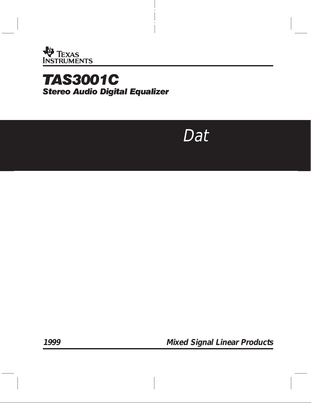
1.2 Functional Block Diagram
Scale
SDIN1
SDIN1
Σ
Parametric EQ
Order IIR Filters)
(Multiple 2
nd
Treble/Bass Volume
Dynamic Range
Compressor
SDIN2
LRCLK
SCLK
Serial Audio
Input Port
Scale
SDIN2
DRC Scale
Factor
SDOUT
1–2
MCLK
CAP_PLL
SDA
SCL
CS1
CS2
Clock
Generator
PLL
12C
Slave
SCLKOUT
LRCLKOUT
Internal Clocks
Internal Control
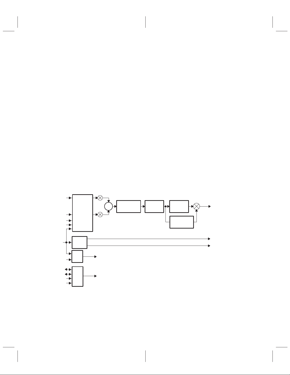
1.3 Terminal Assignments
PW PACKAGE
(TOP VIEW)
AV
AV
NC – No internal connection
1.4 Ordering Information
CS2
1
DV
DV
SDA
SDIN1
SDIN2
SDOUT
MCLK
LRCLK
SCLK
_PLL
SS
_PLL
DD
CAP_PLL
0°C to 70°C TAS3001CPW
SS
DD
SCL
T
2
3
4
5
6
7
8
9
10
11
12
13
14
A
CS1
28
RESERVED
27
NC
26
NC
25
SCLKOUT
24
LRCLKOUT
23
NC
22
NC
21
NC
20
RESET
19
NC
18
NC
17
RESERVED
16
15
RESERVED
PACKAGE
SMALL OUTLINE
(PW)
1–3
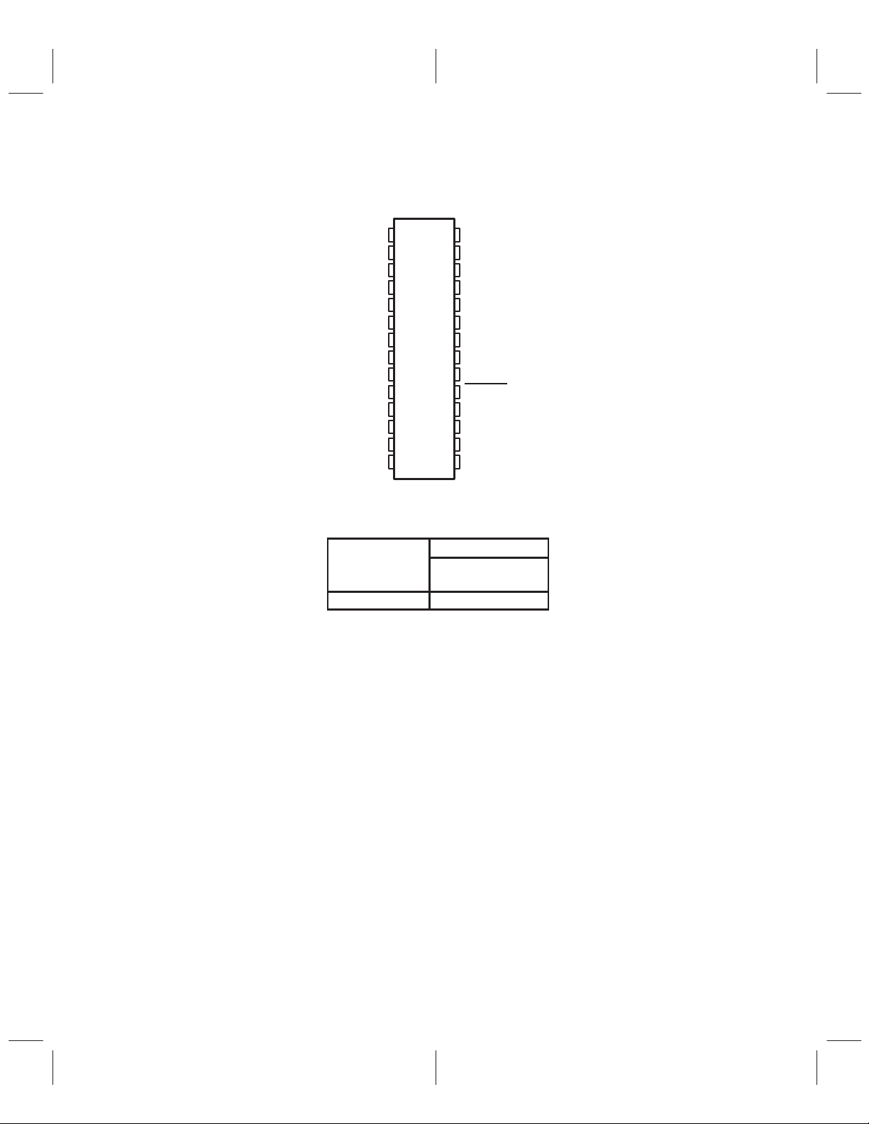
1.5 Terminal Functions
I/O
DESCRIPTION
TERMINAL
NAME NO.
AVDD_PLL 13 I Analog power supply for the PLL
AVSS_PLL 12 I Analog ground for the PLL
CAP_PLL 14 I C1 = 1500 pF // R1 = 27 Ω + C2 = 0.068 µF (recommended)
CS1 28 I I2C address bit A0; low = 0, high = 1
CS2 1 I I2C address bit A1; low = 0, high = 1
DV
DD
DV
SS
LRCLK 10 I I2S left/right clock sampling frequency (fs)
LRCLKOUT 23 O
MCLK 9 I Master clock
NC
RESET 19 I Reset, high = normal operation, low = reinitialize the device
RESERVED 15, 16, 27 Reserved – digital ground for normal operation
SCL 5 I/O Slave serial I2C clock
SCLK 11 I Shift clock (bit clock)
SCLKOUT 24 O
SDA 4 I/O Slave serial I2C data
SDIN1 6 I Serial audio data input one
SDIN2 7 I Serial audio data input two
SDOUT 8 O Serial audio data output
3 I Digital power supply
2 I Digital ground
LRCLK generated from input MCLK (usually 256 fs) – normally routed on
PCB to pin 10 (LRCLK) as input fs sample clock.
17, 18, 20–22,
25, 26
Reserved – No connection for normal operation
SCLK generated from input MCLK (usually 256 fs) – normally routed on
PCB to pin 11 (SCLK) as input 64 fs bit clock.
1–4

2 Description
2.1 Serial Audio Interface
• Programmable serial audio port
2
S, left justified, and right justified
–I
• Dual input data channels (SDIN1 and SDIN2)
– 16-,18-, or 20-bit resolution (see Section 6.1,
• Single output data channel (SDOUT)
Audio Data
)
– 16-,18-, or 20-bit resolution (see Section 6.1,
• Accepts 32 f
• Two I2C programmable address pins (CS1 and CS2)
or 64 fs (SCLK)
s
†
Audio Data
2.2 Serial Control Interface
• I2C slave port
• Downloads EQ coefficients
• Volume, bass, treble, and mixer control
• DRC control
• Write only
2.3 Audio Processing
• Programmable multiband digital parametric EQ (dynamically updateable)
• Programmable volume control (dynamically updateable)
• Soft mute software controlled
• Digital mixing of SDIN1 and SDIN2 with independent gain control
• Programmable bass and treble tone control (dynamically updateable)
• Dynamic range compression (DRC)
2.4 Power Supply
• Digital supply voltage – DVDD, DVSS of 3.3 V
• Analog supply voltage – A V
†
32 fs serial input mode is left justified 16 bit only
_PLL, A VSS_PLL of 3.3 V
DD
)
2–1
2.5 Serial Audio Interface
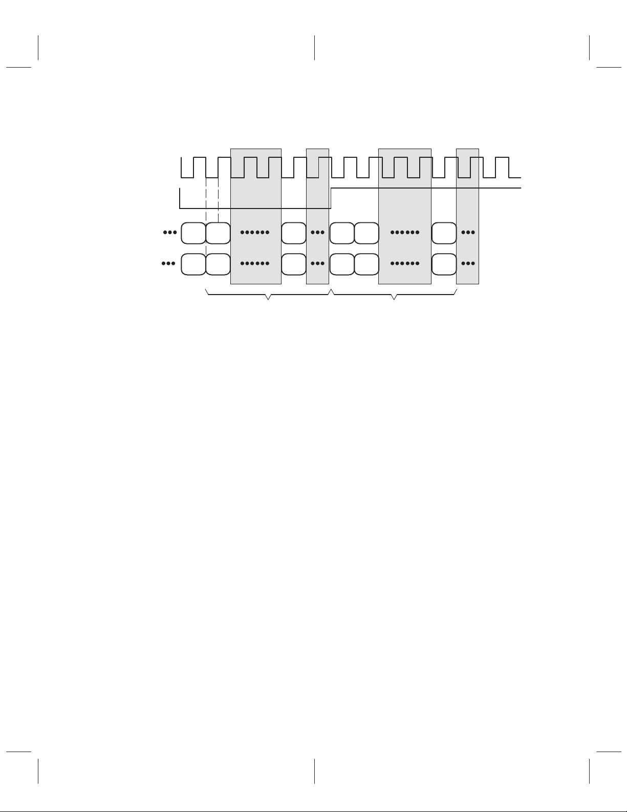
2.5.1 I
2
S Serial Format
SCLK
LRCLK = f
SDOUT
SDIN
s
MSB
X
MSBX
Left Channel Right Channel
LSB
LSB
MSBX
MSBX
Figure 2–1. I2S Compatible Serial Format
2.5.2 Protocol
1. LRCLK = Sampling frequency (fs)
2. Left channel is transmitted when LRCLK is low.
3. SCLK = 64 × LRCLK. SCLK is sometimes referred to as the bit clock.
4. Serial data is sampled with the rising edge of SCLK.
5. Serial data is transmitted on the falling edge of SCLK.
6. LRCLK must have a 50% duty cycle.
2.5.3 Implementation
1. LRCLK and SCLK are both inputs.
2.5.4 Timing
See Figure 4–1 for I2S timing.
LSB
LSB
2–2
 Loading...