

Page 1

l
Data M anua
March 2004 DAV−Audio Products
SLAS226B
Page 2

IMPORTANT NOTICE
Texas Instruments Incorporated and its subsidiaries (TI) reserve the right to make corrections, modifications,
enhancements, improvements, and other changes to its products and services at any time and to discontinue
any product or service without notice. Customers should obtain the latest relevant information before placing
orders and should verify that such information is current and complete. All products are sold subject to TI’s terms
and conditions of sale supplied at the time of order acknowledgment.
TI warrants performance of its hardware products to the specifications applicable at the time of sale in
accordance with TI’s standard warranty. Testing and other quality control techniques are used to the extent TI
deems necessary to support this warranty . Except where mandated by government requirements, testing of all
parameters of each product is not necessarily performed.
TI assumes no liability for applications assistance or customer product design. Customers are responsible for
their products and applications using TI components. To minimize the risks associated with customer products
and applications, customers should provide adequate design and operating safeguards.
TI does not warrant or represent that any license, either express or implied, is granted under any TI patent right,
copyright, mask work right, or other TI intellectual property right relating to any combination, machine, or process
in which TI products or services are used. Information published by TI regarding third-party products or services
does not constitute a license from TI to use such products or services or a warranty or endorsement thereof.
Use of such information may require a license from a third party under the patents or other intellectual property
of the third party, or a license from TI under the patents or other intellectual property of TI.
Reproduction of information in TI data books or data sheets is permissible only if reproduction is without
alteration and is accompanied by all associated warranties, conditions, limitations, and notices. Reproduction
of this information with alteration is an unfair and deceptive business practice. TI is not responsible or liable for
such altered documentation.
Resale of TI products or services with statements different from or beyond the parameters stated by TI for that
product or service voids all express and any implied warranties for the associated TI product or service and
is an unfair and deceptive business practice. TI is not responsible or liable for any such statements.
Following are URLs where you can obtain information on other Texas Instruments products and application
solutions:
Products Applications
Amplifiers amplifier.ti.com Audio www.ti.com/audio
Data Converters dataconverter.ti.com Automotive www.ti.com/automotive
DSP dsp.ti.com Broadband www.ti.com/broadband
Interface interface.ti.com Digital Control www.ti.com/digitalcontrol
Logic logic.ti.com Military www.ti.com/military
Power Mgmt power.ti.com Optical Networking www.ti.com/opticalnetwork
Microcontrollers microcontroller.ti.com Security www.ti.com/security
Telephony www.ti.com/telephony
Video & Imaging www.ti.com/video
Wireless www.ti.com/wireless
Mailing Address: Texas Instruments
Post Office Box 655303 Dallas, Texas 75265
Copyright 2004, Texas Instruments Incorporated
Page 3

Contents
Section Title Page
1 Introduction 1−1. . . . . . . . . . . . . . . . . . . . . . . . . . . . . . . . . . . . . . . . . . . . . . . . . . . . . .
1.1 Description 1−1. . . . . . . . . . . . . . . . . . . . . . . . . . . . . . . . . . . . . . . . . . . . . . . . .
1.2 Overview 1−1. . . . . . . . . . . . . . . . . . . . . . . . . . . . . . . . . . . . . . . . . . . . . . . . . . .
1.3 Features 1−1. . . . . . . . . . . . . . . . . . . . . . . . . . . . . . . . . . . . . . . . . . . . . . . . . . .
1.3.1 Stereo Digital Audio Processing 1−1. . . . . . . . . . . . . . . . . . . . . .
1.3.2 Interfaces 1−2. . . . . . . . . . . . . . . . . . . . . . . . . . . . . . . . . . . . . . . . . .
1.3.3 Electrical and Physical 1−2. . . . . . . . . . . . . . . . . . . . . . . . . . . . . .
1.4 Applications 1−2. . . . . . . . . . . . . . . . . . . . . . . . . . . . . . . . . . . . . . . . . . . . . . . .
1.4.1 Digital Audio Controls 1−2. . . . . . . . . . . . . . . . . . . . . . . . . . . . . . .
1.4.2 Equalization 1−2. . . . . . . . . . . . . . . . . . . . . . . . . . . . . . . . . . . . . . . .
1.4.3 Loudspeaker Active Crossovers 1−2. . . . . . . . . . . . . . . . . . . . . .
1.5 Functional Block Diagram 1−3. . . . . . . . . . . . . . . . . . . . . . . . . . . . . . . . . . . .
1.6 Mixing/Input Scaling 1−3. . . . . . . . . . . . . . . . . . . . . . . . . . . . . . . . . . . . . . . . .
1.7 High-Precision, Second-Order Biquad Filter Structure 1−4. . . . . . . . . . . .
1.8 Bass and Treble Controls 1−6. . . . . . . . . . . . . . . . . . . . . . . . . . . . . . . . . . . . .
1.9 Soft Volume and True Soft Mute 1−6. . . . . . . . . . . . . . . . . . . . . . . . . . . . . . .
1.10 Reliability and Flexibility of Digital Filtering 1−7. . . . . . . . . . . . . . . . . . . . . .
1.11 Pin Assignments 1−7. . . . . . . . . . . . . . . . . . . . . . . . . . . . . . . . . . . . . . . . . . . .
1.12 Pin Functions 1−8. . . . . . . . . . . . . . . . . . . . . . . . . . . . . . . . . . . . . . . . . . . . . . .
1.13 Ordering Information 1−8. . . . . . . . . . . . . . . . . . . . . . . . . . . . . . . . . . . . . . . . .
1.14 Power Supply 1−8. . . . . . . . . . . . . . . . . . . . . . . . . . . . . . . . . . . . . . . . . . . . . . .
2 Audio Data Formats 2−1. . . . . . . . . . . . . . . . . . . . . . . . . . . . . . . . . . . . . . . . . . . . . . .
2.1 Serial Audio Interface 2−1. . . . . . . . . . . . . . . . . . . . . . . . . . . . . . . . . . . . . . . .
2.1.1 I
2.1.2 Left-Justified Serial Format 2−3. . . . . . . . . . . . . . . . . . . . . . . . . . .
2.1.3 Right-Justified Serial Format 2−4. . . . . . . . . . . . . . . . . . . . . . . . .
2.2 LRCLKOUT and SCLKOUT 2−4. . . . . . . . . . . . . . . . . . . . . . . . . . . . . . . . . . .
3 Serial Control Interface (I
3.1 I
2
C Protocol 3−1. . . . . . . . . . . . . . . . . . . . . . . . . . . . . . . . . . . . . . . . . . . . . . . .
3.2 Operation 3−2. . . . . . . . . . . . . . . . . . . . . . . . . . . . . . . . . . . . . . . . . . . . . . . . . .
3.2.1 Write Cycle Example 3−2. . . . . . . . . . . . . . . . . . . . . . . . . . . . . . . .
3.2.2 I
3.2.3 Resetting the TAS3001 I
3.2.4 Power-Up Conditions 3−3. . . . . . . . . . . . . . . . . . . . . . . . . . . . . . . .
3.2.5 I
4 Digital Audio Processor 4−1. . . . . . . . . . . . . . . . . . . . . . . . . . . . . . . . . . . . . . . . . . .
4.1 Input Mixer Control 4−1. . . . . . . . . . . . . . . . . . . . . . . . . . . . . . . . . . . . . . . . . .
2
S Serial Format 2−2. . . . . . . . . . . . . . . . . . . . . . . . . . . . . . . . . . .
2
C) 3−1. . . . . . . . . . . . . . . . . . . . . . . . . . . . . . . . . . . . . . .
2
C Timing and Wait Cycles 3−2. . . . . . . . . . . . . . . . . . . . . . . . . .
2
C Interface 3−3. . . . . . . . . . . . . . . . . .
2
C Serial Port Timing 3−4. . . . . . . . . . . . . . . . . . . . . . . . . . . . . . .
iii
Page 4

4.2 Biquad Block 4−1. . . . . . . . . . . . . . . . . . . . . . . . . . . . . . . . . . . . . . . . . . . . . . . .
4.2.1 Filter Coefficients 4−1. . . . . . . . . . . . . . . . . . . . . . . . . . . . . . . . . . .
4.3 Volume Control Functions 4−1. . . . . . . . . . . . . . . . . . . . . . . . . . . . . . . . . . . .
4.3.1 Soft Volume Update 4−1. . . . . . . . . . . . . . . . . . . . . . . . . . . . . . . . .
4.3.2 Software Soft Mute 4−2. . . . . . . . . . . . . . . . . . . . . . . . . . . . . . . . .
4.4 Tone Controls 4−2. . . . . . . . . . . . . . . . . . . . . . . . . . . . . . . . . . . . . . . . . . . . . . .
4.4.1 Treble Control 4−2. . . . . . . . . . . . . . . . . . . . . . . . . . . . . . . . . . . . . .
4.4.2 Bass Control 4−2. . . . . . . . . . . . . . . . . . . . . . . . . . . . . . . . . . . . . . .
4.4.3 Frequency Dependence of Treble and Bass Controls 4−2. . . .
5 Device Operation 5−1. . . . . . . . . . . . . . . . . . . . . . . . . . . . . . . . . . . . . . . . . . . . . . . . .
5.1 Device Initialization 5−1. . . . . . . . . . . . . . . . . . . . . . . . . . . . . . . . . . . . . . . . . .
5.1.1 Reset 5−1. . . . . . . . . . . . . . . . . . . . . . . . . . . . . . . . . . . . . . . . . . . . .
5.1.2 Device Power On and System Reset 5−1. . . . . . . . . . . . . . . . . .
5.1.3 Fast Load 5−1. . . . . . . . . . . . . . . . . . . . . . . . . . . . . . . . . . . . . . . . . .
5.2 Power Consumption 5−2. . . . . . . . . . . . . . . . . . . . . . . . . . . . . . . . . . . . . . . . .
5.3 Power Down and Start-Up 5−2. . . . . . . . . . . . . . . . . . . . . . . . . . . . . . . . . . . .
6 Electrical Characteristics 6−1. . . . . . . . . . . . . . . . . . . . . . . . . . . . . . . . . . . . . . . . . .
6.1 Absolute Maximum Ratings Over Operating Free-Air
Temperature Range 6−1. . . . . . . . . . . . . . . . . . . . . . . . . . . . . . . . . . . . . . . . .
6.2 Recommended Operating Conditions 6−1. . . . . . . . . . . . . . . . . . . . . . . . . .
6.3 Power Consumption 6−1. . . . . . . . . . . . . . . . . . . . . . . . . . . . . . . . . . . . . . . . .
6.4 Static Digital Specifications 6−1. . . . . . . . . . . . . . . . . . . . . . . . . . . . . . . . . . .
7 Measured Audio Performance for Some Typical Examples 7−1. . . . . . . . . . .
8 Using the TAS3001 in a System 8−1. . . . . . . . . . . . . . . . . . . . . . . . . . . . . . . . . . . .
8.1 TAS3001 Applications 8−1. . . . . . . . . . . . . . . . . . . . . . . . . . . . . . . . . . . . . . . .
8.2 Measurement-Based Speaker Correction 8−2. . . . . . . . . . . . . . . . . . . . . . .
8.3 Sound-Based Speaker Correction 8−3. . . . . . . . . . . . . . . . . . . . . . . . . . . . .
8.4 Loudspeaker Equalization Example 8−3. . . . . . . . . . . . . . . . . . . . . . . . . . . .
8.5 Speaker Correction and Equalization 8−5. . . . . . . . . . . . . . . . . . . . . . . . . . .
8.6 The TAS3001 Can Implement Nearly Any Second-Order IIR Filter 8−5.
8.7 Converting Analog Filters to Digital 8−7. . . . . . . . . . . . . . . . . . . . . . . . . . . .
9 Automatic Loudspeaker Equalizer (ALE) 9−1. . . . . . . . . . . . . . . . . . . . . . . . . . . .
9.1 Automatic Generation of Equalization Filters Given a Measurement 9−1
9.2 Automatic Approximation of an Equalization Curve 9−1. . . . . . . . . . . . . . .
9.3 Manual Filter Design 9−1. . . . . . . . . . . . . . . . . . . . . . . . . . . . . . . . . . . . . . . . .
9.4 Conversion of Decimal Filter Coefficients to the TAS3001 Format 9−1. .
9.5 Editing of TAS3001 File Format 9−1. . . . . . . . . . . . . . . . . . . . . . . . . . . . . . .
9.6 Examples of the Filter Types Available From ALE 2.1 9−1. . . . . . . . . . . .
10 FilterBuilder and FilterMaker 10−1. . . . . . . . . . . . . . . . . . . . . . . . . . . . . . . . . . . . . . .
A Software Interface A−1. . . . . . . . . . . . . . . . . . . . . . . . . . . . . . . . . . . . . . . . . . . . . . . .
A.1 Main Control Register (MCR) A−2. . . . . . . . . . . . . . . . . . . . . . . . . . . . . . . . .
B Mechanical Information B−1. . . . . . . . . . . . . . . . . . . . . . . . . . . . . . . . . . . . . . . . . . .
iv
Page 5

List of Illustrations
Figure Title Page
1−1 TAS3001 Signal Flow 1−3. . . . . . . . . . . . . . . . . . . . . . . . . . . . . . . . . . . . . . . . . . .
1−2 Examples of High-Pass Filters 1−4. . . . . . . . . . . . . . . . . . . . . . . . . . . . . . . . . . . .
1−3 Examples of Equalization Filters 1−4. . . . . . . . . . . . . . . . . . . . . . . . . . . . . . . . . .
1−4 Bass and Treble Shelves 1−5. . . . . . . . . . . . . . . . . . . . . . . . . . . . . . . . . . . . . . . .
1−5 Multiple Filter Response 1−5. . . . . . . . . . . . . . . . . . . . . . . . . . . . . . . . . . . . . . . . .
1−6 Combed Response of the Multiple Filters 1−5. . . . . . . . . . . . . . . . . . . . . . . . . .
1−7 Bass and Treble Filters 1−6. . . . . . . . . . . . . . . . . . . . . . . . . . . . . . . . . . . . . . . . . .
1−8 TAS3001 Pin Location Diagram 1−7. . . . . . . . . . . . . . . . . . . . . . . . . . . . . . . . . . .
2−1 I
2−2 For Right/Left Justified, I
2−3 Left-Justified Serial Format 2−3. . . . . . . . . . . . . . . . . . . . . . . . . . . . . . . . . . . . . . .
2−4 Right-Justified Serial Format 2−4. . . . . . . . . . . . . . . . . . . . . . . . . . . . . . . . . . . . .
2−5 Master Mode 2−4. . . . . . . . . . . . . . . . . . . . . . . . . . . . . . . . . . . . . . . . . . . . . . . . . . .
2−6 Slave Mode 2−5. . . . . . . . . . . . . . . . . . . . . . . . . . . . . . . . . . . . . . . . . . . . . . . . . . . .
3−1 Typical I
3−2 Write Cycle Example 3−2. . . . . . . . . . . . . . . . . . . . . . . . . . . . . . . . . . . . . . . . . . . .
3−3 Wait Cycle Example 3−2. . . . . . . . . . . . . . . . . . . . . . . . . . . . . . . . . . . . . . . . . . . . .
3−4 I2C Serial Port Timing 3−4. . . . . . . . . . . . . . . . . . . . . . . . . . . . . . . . . . . . . . . . . . .
4−1 Cascaded Biquad Filters 4−1. . . . . . . . . . . . . . . . . . . . . . . . . . . . . . . . . . . . . . . . .
4−2 Audio Processing Architecture 4−2. . . . . . . . . . . . . . . . . . . . . . . . . . . . . . . . . . . .
5−1 Main Control Register (MCR) 5−1. . . . . . . . . . . . . . . . . . . . . . . . . . . . . . . . . . . . .
5−2 Power-Down Timing 5−2. . . . . . . . . . . . . . . . . . . . . . . . . . . . . . . . . . . . . . . . . . . . .
5−3 Start-Up Timing 5−2. . . . . . . . . . . . . . . . . . . . . . . . . . . . . . . . . . . . . . . . . . . . . . . . .
6−1 Typical TAS3001 Connection 6−2. . . . . . . . . . . . . . . . . . . . . . . . . . . . . . . . . . . . .
7−1 Audio Performance Measurement System 7−1. . . . . . . . . . . . . . . . . . . . . . . . .
7−2 Audio Performance Test Filters 7−2. . . . . . . . . . . . . . . . . . . . . . . . . . . . . . . . . . .
8−1 TAS3001 as a System Equalizer 8−1. . . . . . . . . . . . . . . . . . . . . . . . . . . . . . . . . .
8−2 TAS3001 as a Crossover and Equalizer 8−2. . . . . . . . . . . . . . . . . . . . . . . . . . .
8−3 Typical Small Loudspeaker Response 8−3. . . . . . . . . . . . . . . . . . . . . . . . . . . . .
8−4 Preparation for Equalization 8−4. . . . . . . . . . . . . . . . . . . . . . . . . . . . . . . . . . . . . .
8−5 After Equalization 8−4. . . . . . . . . . . . . . . . . . . . . . . . . . . . . . . . . . . . . . . . . . . . . . .
8−7 Equalization Filters 8−5. . . . . . . . . . . . . . . . . . . . . . . . . . . . . . . . . . . . . . . . . . . . . .
8−8 Individual Filters 8−6. . . . . . . . . . . . . . . . . . . . . . . . . . . . . . . . . . . . . . . . . . . . . . . .
2
S-Compatible Serial Format 2−2. . . . . . . . . . . . . . . . . . . . . . . . . . . . . . . . . . . .
2
S, Left/Left Justified Serial Protocols 2−3. . . . . . . .
2
C Data Transfer Sequence 3−1. . . . . . . . . . . . . . . . . . . . . . . . . . . . . .
v
Page 6

List of Illustrations (Continued)
8−9 Combined Response 8−6. . . . . . . . . . . . . . . . . . . . . . . . . . . . . . . . . . . . . . . . . . . .
9−1 Equalization Filters 9−2. . . . . . . . . . . . . . . . . . . . . . . . . . . . . . . . . . . . . . . . . . . . . .
9−2 High- and Low-Pass Filters 9−2. . . . . . . . . . . . . . . . . . . . . . . . . . . . . . . . . . . . . .
9−3 Treble and Bass Shelf Filters 9−3. . . . . . . . . . . . . . . . . . . . . . . . . . . . . . . . . . . . .
9−4 Notch Filters 9−3. . . . . . . . . . . . . . . . . . . . . . . . . . . . . . . . . . . . . . . . . . . . . . . . . . .
List of Tables
Table Title Page
2−1 Serial Interface Input Options 2−1. . . . . . . . . . . . . . . . . . . . . . . . . . . . . . . . . . . . .
2−2 Serial Interface Output Options 2−1. . . . . . . . . . . . . . . . . . . . . . . . . . . . . . . . . . .
2
3−1 I
3−2 TAS3001 I
3−3 Write Cycle Example 3−2. . . . . . . . . . . . . . . . . . . . . . . . . . . . . . . . . . . . . . . . . . . .
3−4 I
4−1 Bass Control Corner Frequencies 4−2. . . . . . . . . . . . . . . . . . . . . . . . . . . . . . . . .
4−2 Treble Control Corner Frequencies 4−2. . . . . . . . . . . . . . . . . . . . . . . . . . . . . . . .
7−1 Audio Filter Performance 7−1. . . . . . . . . . . . . . . . . . . . . . . . . . . . . . . . . . . . . . . .
A−1 Register Map A−1. . . . . . . . . . . . . . . . . . . . . . . . . . . . . . . . . . . . . . . . . . . . . . . . . . .
A−2 Main Control Register (MCR) A−2. . . . . . . . . . . . . . . . . . . . . . . . . . . . . . . . . . . . .
A−3 Main Control Register (MCR) Description A−2. . . . . . . . . . . . . . . . . . . . . . . . . .
A−4 Volume Gain Values A−3. . . . . . . . . . . . . . . . . . . . . . . . . . . . . . . . . . . . . . . . . . . .
A−5 Treble Control Register A−4. . . . . . . . . . . . . . . . . . . . . . . . . . . . . . . . . . . . . . . . . .
A−6 Bass Control Register A−4. . . . . . . . . . . . . . . . . . . . . . . . . . . . . . . . . . . . . . . . . . .
A−7 Mixer1 and Mixer2 Gain Values A−5. . . . . . . . . . . . . . . . . . . . . . . . . . . . . . . . . . .
C Protocol Definitions 3−1. . . . . . . . . . . . . . . . . . . . . . . . . . . . . . . . . . . . . . . . . .
2
C Address 3−2. . . . . . . . . . . . . . . . . . . . . . . . . . . . . . . . . . . . . . . . . . .
2
C Wait States 3−3. . . . . . . . . . . . . . . . . . . . . . . . . . . . . . . . . . . . . . . . . . . . . . . . .
vi
Page 7

1 Introduction
1.1 Description
The TAS3001 is a high-quality, fixed-function, 32-bit digital audio processor. This device contains a number of built-in
processing functions including mixing/scaling of two digital inputs, bass and treble controls, six cascaded stereo
high-precision, limit-cycle-free, second-order IIR filters, soft volume, and soft mute.
These functions can be controlled by specifying the desired operating parameters using the I
The TAS3001 architecture preserves high-quality audio by using a 32-bit data path, 24 × 32-bit multiplies, and up to
56 bits of precision for some internal calculations. By using 24-bit filter coefficients, the TAS3001 can implement
practically any second-order IIR filter with outstanding fidelity.
1.2 Overview
The TAS3001 is a 32-bit audio signal processor that provides mixing of two digital inputs and digital parametric
equalization. In addition, this device provides high-quality, soft digital volume, bass, and treble controls. All control
parameters are uploaded through the I
The TAS3001 has four audio processing blocks as shown in Figure 1−1.
• Two digital stereo audio inputs that can be scaled and mixed prior to processing.
• Parametric EQ that consists of six cascaded independent second-order IIR filters for each of the left and
right independent channels. Each filter has five 24-bit coefficients that can be configured into many different
filter functions, such as band-pass, high-pass, low-pass, shelves, notch, all-pass, high-/low-pass with shelf,
etc.
2
C port from an outside MCU.
2
C interface.
• Digital bass and treble controls
• Digital soft volume and mute
The TAS3001 device uses a system clock that is generated by the internal phase-locked loop (PLL). An external
master clock (MCLK) of 256 times the sampling frequency provides the reference clock for the PLL.
The TAS3001 device supports several serial data formats (I
16, 18, or 20. The sampling frequencies (f
) that are supported include 32 kHz, 44.1 kHz, 48 kHz and 96 kHz.
s
2
S, left justified, right justified) with data word lengths of
1.3 Features
1.3.1 Stereo Digital Audio Processing
• Supports nine serial data formats. Receive and transmit serial data formats may be different.
• Programmable two-input digital mixer
• Programmable six-band digital parametric EQ
• Programmable digital bass and treble controls
• Programmable digital volume control with soft mute
• 108-dB dynamic range
• Sample rates from 32 kHz to 96 kHz
1.3.2 Interfaces
• Two serial digital input channels
• Single serial digital output channel
2
• Serial I
C control channel
1−1
Page 8

1.3.3 Electrical and Physical
• Single 3.3-V power supply
• 28-pin PW package
• Low-power standby
1.4 Applications
1.4.1 Digital Audio Controls
The TAS3001 can be used to provide a high-quality digital system control of volume, bass, treble, and parametric
equalization.
1.4.2 Equalization
The TAS3001 can be used to perform parametric equalization to correct the frequency response of loudspeakers or
microphones. The TAS3001 corrects the response by applying filters to compensate for the response irregularities
of the transducers.
1.4.3 Loudspeaker Active Crossovers
The TAS3001 can be used to implement an active crossover for multi-way loudspeaker systems.
1−2
Page 9
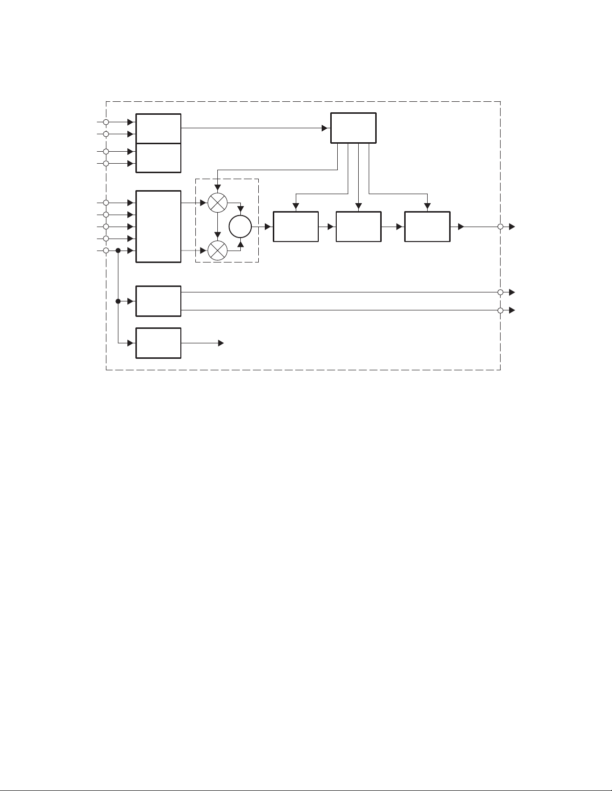
1.5 Functional Block Diagram
SDA
SCL
CS1
CS2
SDIN1
SDIN2
LRCLK
SCLK
MCLK
4
5
28
1
6
7
10
11
9
I2C
Slave
Address
Select
Serial
Audio
Input
Port
Clock
Generator
PLL
Σ
2-Channel
Stereo Mixer
Internal Clocks
6 Biquad
Filters
System
Control
Treble/
Bass
Volume
23
24
8
SDOUT
LRCLKOUT
SCLKOUT
Figure 1−1. TAS3001 Signal Flow
Figure 1−1 shows the signal flow from the inputs (SDIN1 and SDIN2) though each processing stage to the output
(SDOUT) where it is passed to an external DAC, digital amplifier, or other subsequent digital data processing stage.
Each of these audio processing functions is discussed in more detail in the following sections.
1.6 Mixing/Input Scaling
The TAS3001 is equipped with a dual-input stereo digital mixer. Thi s m ixe r pe rmi ts eac h i nput to sc ale d ( −∞ to +18 dB)
independently. A stereo sum of the scaled results is produced.
1−3
Page 10
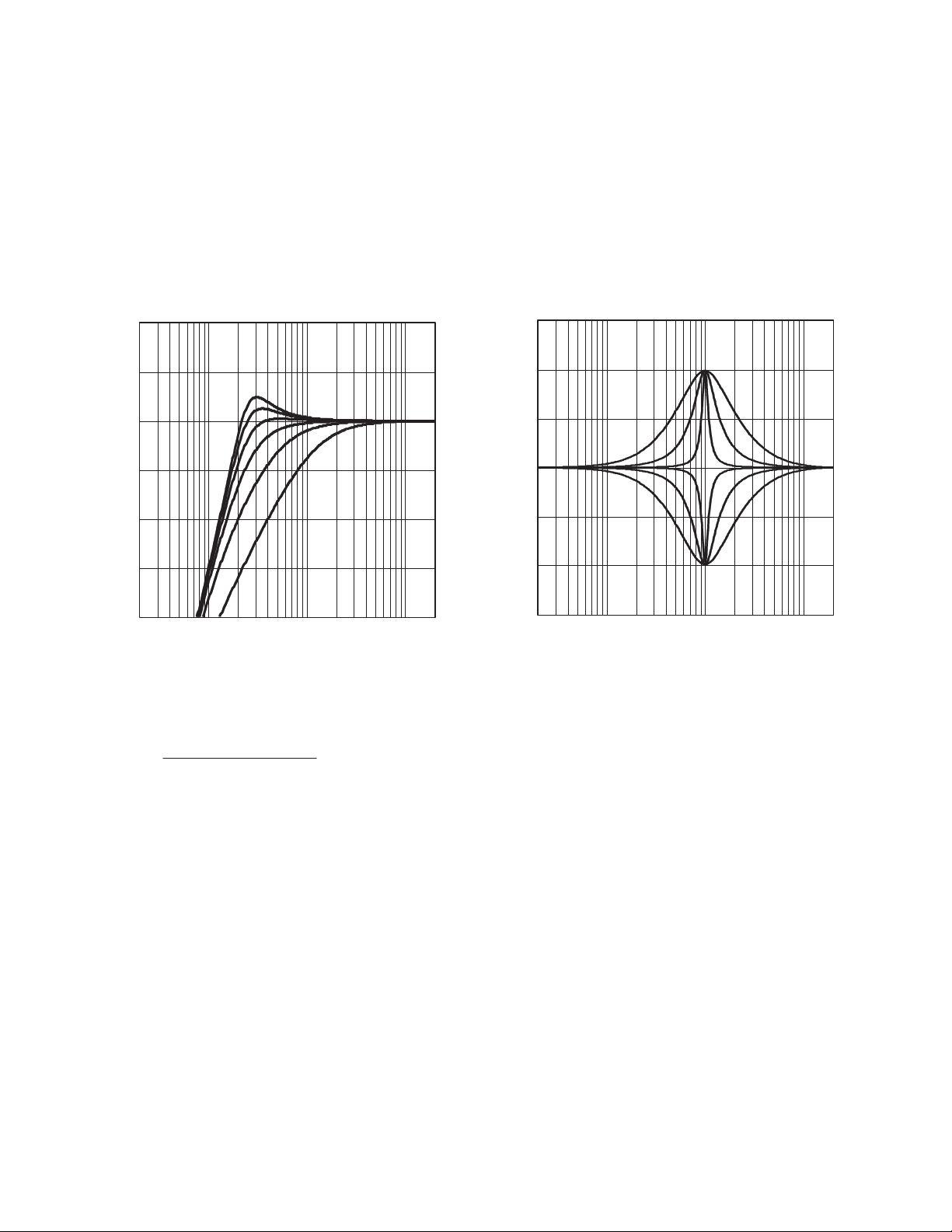
1.7 High-Precision, Second-Order Biquad Filter Structure
The TAS3001 has six cascaded biquad filters for the left and right channels to permit parametric equalization and
filtering of the input signal. Each biquad is able to specify a wide variety of first- and second-order filter types, including
high-pass, low-pass, band-pass, band-block, notch, and all-pass filter types. Examples of a few of the filters that can
be implemented by the TAS3001 shapes are illustrated in Figure 1−2 though Figure 1−6.
ATTENUATION
vs
FREQUENCY
10
5
0
−5
Attenuation − dB
−10
−15
−20
100 1k 10k
f − Frequency − Hz
Figure 1−2. Examples of High-Pass Filters
The biquad structure is of the form:
ATTENUATION
vs
FREQUENCY
15
10
5
0
Attenuation − dB
−5
−10
−15
100 1k 10k
f − Frequency − Hz
Figure 1−3. Examples of Equalization Filters
H(z) +
b0) b1Z–1) b2Z
1 ) a1Z–1) a2Z
–2
–2
Coefficients are downloaded to the TAS3001 registers in 4.20 format.
1−4
Page 11
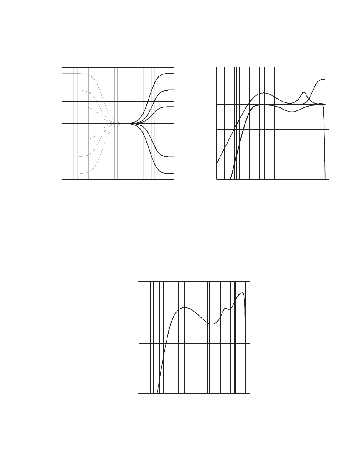
10
ATTENUATION
ATTENUATION
vs
FREQUENCY
vs
FREQUENCY
15
8
6
4
2
0
−2
Attenuation − dB
−4
−6
−8
−10
100 1k 10k
f − Frequency − Hz
10
5
0
−5
−10
Attenuation − dB
−15
−20
−25
−30
10 1k 10k1 100
f − Frequency − Hz
Figure 1−4. Bass and Treble Shelves Figure 1−5. Multiple Filter Response
The TAS3001 provides a zero-input limit-cycle-free second-order IIR filtering structure that implements a direct form
I filter structure. This architecture preserves high-quality audio by using a 32-bit data path, 24 × 32-bit multiplies, and
56 bits of precision for some internal calculations. By using 24-bit filter coefficients, the TAS3001 can implement
practically any second-order IIR filter with outstanding fidelity.
Texas Instruments has several tools that provide a powerful and flexible means to develop applications using the
TAS3001. Chapter 8 provides examples of how the TAS3001 can be used to meet various system needs.
ATTENUATION
vs
15
FREQUENCY
10
5
0
−5
−10
Attenuation − dB
−15
−20
−25
−30
10 1k 10k1 100
f − Frequency − Hz
Figure 1−6. Combed Response of the Multiple Filters
1−5
Page 12
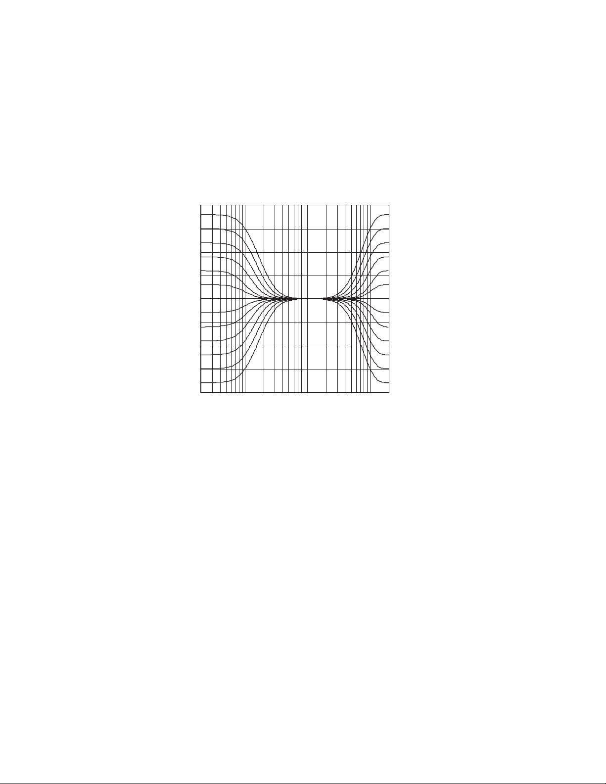
1.8 Bass and Treble Controls
The TAS3001 has bass and treble controls that can be adjusted dynamically. These controls can be adjusted
throughout their entire range of 18 dB to –18 dB without experiencing any pops, clicks, or other audible artifacts. This
permits the user to have a listening experience much like what is experienced when adjusting high-quality analog
controls.
Figure 1−7 shows the response for the bass and treble filters plotted at 3-dB intervals for 44.1-kHz sample-rate data.
ATTENUATION
vs
FREQUENCY
20
15
10
5
0
−5
Attenuation − dB
−10
−15
−20
100 1k 10k
f − Frequency − Hz
Figure 1−7. Bass and Treble Filters
1.9 Soft Volume and True Soft Mute
The TAS3001 contains a Texas Instruments proprietary soft volume update. This allows a smooth and
pleasant-sounding change from one volume level to another over the entire range of volume (18 dB to mute). The
2
volume is adjustable by downloading a 4.20 gain coefficient through the I
C interface.
Mute is implemented by loading all zeros in the volume control register. This causes the volume to ramp down over
2048 samples to a final output of zero (−∞ dB).
1.10 Reliability and Flexibility of Digital Filtering
Digital filtering provides outstanding consistency, reliability, and flexibility. Once a digital filter is designed and tested
in the system, it continues to perform in the same manner without change. Because digital filters are computed, their
performance is exceedingly consistent and does not change due to variations in component matching, tolerances,
environmental conditions, aging, or the effects of moisture and dust. Analog filters, however, are affected by all of
these. The performance of analog filters can be improved, in part, by using high-quality precision components but
this comes with a higher comparable cost.
One of the greatest strengths of a digital filter is its flexibility. Each filter is completely specified by five 24-bit
coefficients. By modifying the value of one or more of the filter coefficients, both the filter value and filter type are
changed. In a system, these modifications produce different crossover curves, different equalization curves, different
sound effects (by changing the relative phase of the left and right loudspeakers) or different user graphical
equalization settings.
1−6
Page 13
Attempting similar changes in an analog filter would require component changes and potentially a new circuit layout.
The flexibility of digital filtering provides a particular advantage to digital equalization. Because of its programmability,
a single design using digital filtering can provide a wide range of filtering functions. As a result, this one design can
span a number of applications.
For a product that is in production, digital filtering can permit equalization changes with minimal cost impact because
of this programmability.
One concern about digital filters is that some implementations have been prone to zero-input limit cycles. This is a
condition where the filter oscillates at a low level when no signal is presented. In a digital audio system, this condition
may present itself as a tone or low-level noise. The TAS3001 has a patent-pending technique to combat this problem.
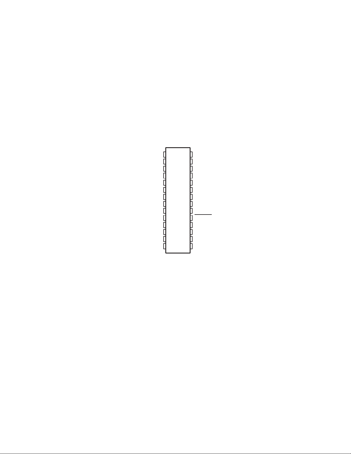
1.11 Pin Assignments
PW PACKAGE
(TOP VIEW)
CS2
1
DV
DV
SDIN1
SDIN2
SDOUT
MCLK
LRCLK
SCLK
AV
_PLL
SS
AV
_PLL
DD
CAP_PLL
NC − No internal connection
SS
DD
SDA
SCL
2
3
4
5
6
7
8
9
10
11
12
13
14
CS1
28
RESERVED
27
NC
26
NC
25
SCLKOUT
24
LRCLKOUT
23
NC
22
NC
21
NC
20
RESET
19
NC
18
NC
17
POWERDOWN
16
15
RESERVED
Figure 1−8. TAS3001 Pin Location Diagram
1−7
Page 14
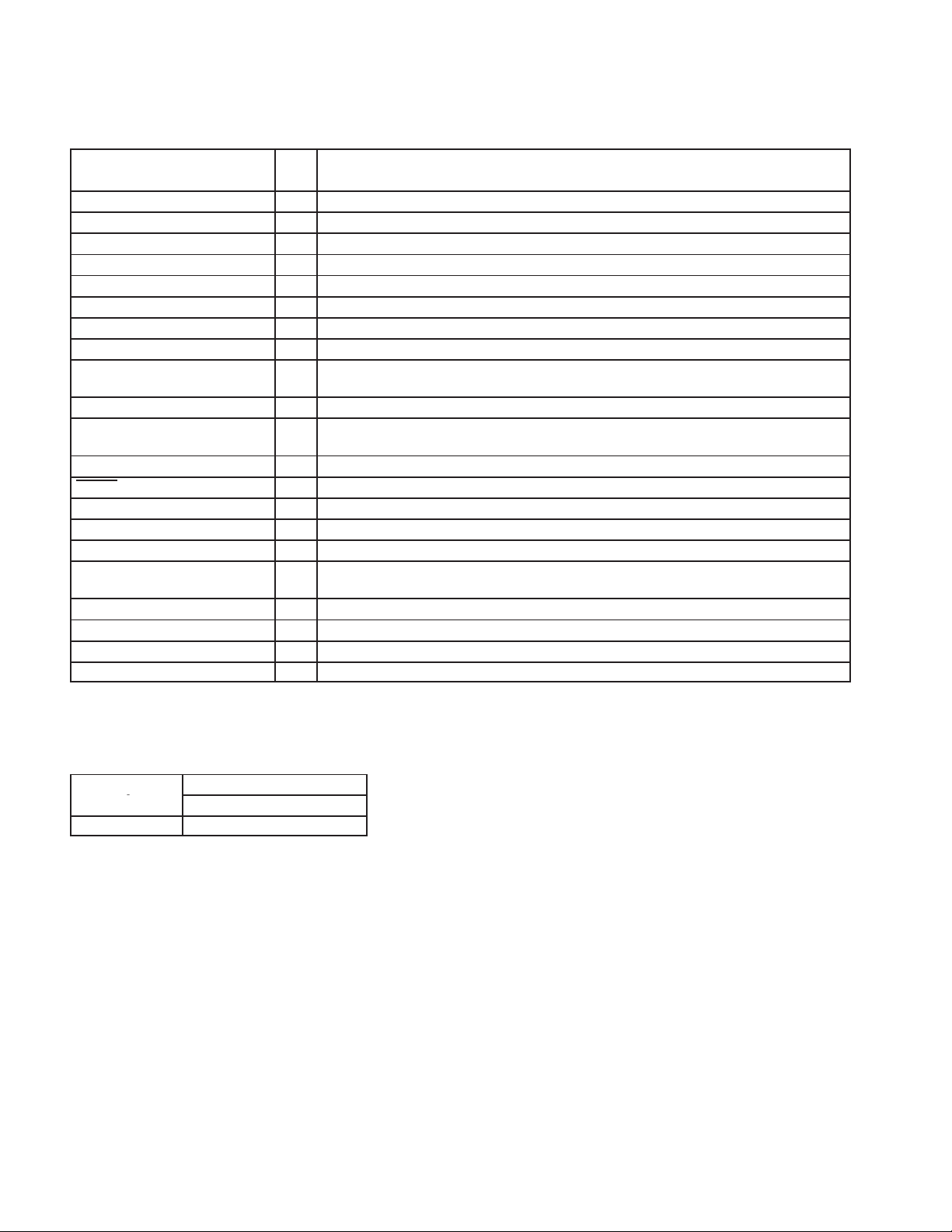
1.12 Pin Functions
I/O
DESCRIPTION
T
TERMINAL
NAME NO.
AVDD_PLL 13 I Analog power supply for the PLL
AVSS_PLL 12 I Analog ground for the PLL
CAP_PLL 14 I C1 = 1500 pF // R1 = 27 Ω + C2 = 0.068 µF (recommended)
CS1 28 I I2C address bit A0; low = 0, high = 1
CS2 1 I I2C address bit A1; low = 0, high = 1
DV
DD
DV
SS
LRCLK 10 I I2S left/right clock sampling frequency (fs)
LRCLKOUT 23 O
MCLK 9 I Master clock (256 x fs)
NC
POWERDOWN 16 I Powerdown input
RESET 19 I Reset, high = normal operation, low = reinitialize the device
RESERVED 15, 27 Reserved − digital ground for normal operation
SCL 5 I/O Slave serial I2C clock
SCLK 11 I Shift clock (bit clock)
SCLKOUT 24 O
SDA 4 I/O Slave serial I2C data
SDIN1 6 I Serial audio data input one
SDIN2 7 I Serial audio data input two
SDOUT 8 O Serial audio data output
NOTE: Reset and other control functions require MCLK to be running. The system reset operation is a synchronous operation and requires a
minimum of four MCLK cycles to reset the device.
3 I Digital power supply
2 I Digital ground
LRCLK generated from input MCLK (usually 256 fs) − normally routed on PCB to pin 10
(LRCLK) as input fs sample clock.
17, 18, 20−22,
25, 26
Reserved − No connection for normal operation
SCLK generated from input MCLK (usually 256 fs) − normally routed on PCB to pin 11 (SCLK)
as input 64 fs bit clock.
1.13 Ordering Information
A
0°C to 70°C TAS3001CPW
PACKAGE
SMALL OUTLINE (PW)
1.14 Power Supply
• Digital supply voltage—DVDD, DVSS of 3.3 V
• Analog supply voltage—AV
NOTE: AV
1−8
DD
and AVSS for the PLL are derived from the digital supply and digital ground.
DD−
PLL, AV
PLL of 3.3 V
SS−
Page 15
2 Audio Data Formats
2.1 Serial Audio Interface
The TAS3001 operates in digital audio slave mode only. The TAS3001 supports three serial audio data formats: I2S,
left-justified, and right-justified. Data word lengths of 16, 18, and 20 bits are supported.
Data is input into SDIN1 and SDIN2 under the influence of the master clock (MCLK), left/right clock (LRCLK), and
shift clock (SCLK) inputs.
Data is output on the SDOUT pin under the influence of the master clock (MCLK) input plus the left/right clock
(LRCLKOUT) and shift clock (SCLKOUT) outputs. LRCLKOUT and SCLKOUT are generated from the MCLK input
(usually at 256 × f
the input 64 × f
The TAS3001 device is compatible with 10 different serial interfaces. Available interface options are I
right-justified, and left-justified. Table 2−1 and Table 2−2 indicate how the 10 options are selected using the I
and the main control register (MCR, I
with SCLK at 64 × f
Figure 2−1 through Figure 2−4 illustrate the relationship between the SCLK, LRCLK, and the serial data input and
output protocol options.
). Typically these are routed on the PCB to LRCLK (as the input fs sample clock) and SCLK (as
s
bit clock).
s
2
C address 01h). All serial interface options at either 16, 18, or 20 bits operate
. The 16-bit mode, left-justified, can operate at 32 × fs or 64 × fs.
s
Table 2−1. Serial Interface Input Options
MODE
0 0 00 00 16-bit, left-justified, 32 × f
1 1 00 00 16-bit, left-justified, 64 × f
2 1 01 00 16-bit, right-justified, 64 × f
3 1 10 00 16-bit, I2S, 64 × f
4 1 00 01 18-bit, left-justified, 64 × f
5 1 01 01 18-bit, right-justified, 64 × f
6 1 10 01 18-bit, I2S, 64 × f
7 1 00 10 20-bit, left-justified, 64 × f
8 1 01 10 20-bit, right-justified, 64 × f
9 1 10 10 20-bit, I2S, 64 × f
MCR BIT 6SCMCR BITS 3−2
F(1,0)
MCR BITS 1−0
W(1,0)
SERIAL INTERFACE
SDIN1, SDIN2
s
s
s
s
s
s
s
s
s
s
Table 2−2. Serial Interface Output Options
MODE
0 0 00 00 16-bit, left-justified, 32 × f
1 1 00 00 16-bit, left-justified, 64 × f
2 1 01 00 16-bit, right-justified, 64 × f
3 1 10 00 16-bit, I2S, 64 × f
4 1 00 01 18-bit, left-justified, 64 × f
5 1 01 01 18-bit, right-justified, 64 × f
6 1 10 01 18-bit, I2S, 64 × f
7 1 00 10 20-bit, left-justified, 64 × f
8 1 01 10 20-bit, right-justified, 64 × f
9 1 10 10 20-bit, I2S, 64 × f
MCR BIT 6SCMCR BITS 5−4
E(1,0)
MCR BITS 1−0
W(1,0)
SERIAL INTERFACE
SDOUT
s
s
s
s
s
s
s
s
s
s
2
C bus
2
S,
2−1
Page 16
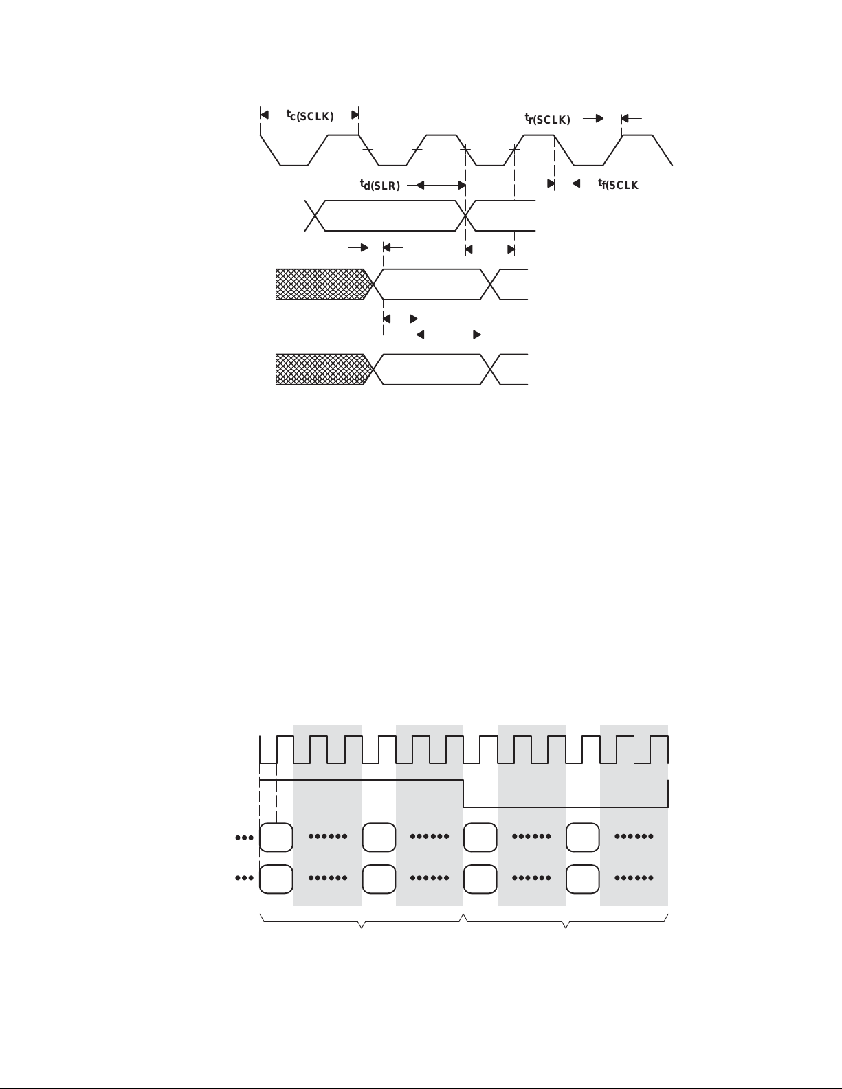
2.1.1 I2S Serial Format
The following are characteristics of this protocol:
• LRCLK is the left/right clock. The left channel is transmitted when LRCLK is low. The right channel is
transmitted when LRCLK is high.
• SDIN is sampled with the rising edge of SCLK.
• SDOUT is transmitted on the falling edge of SCLK.
• LRCK must have a 50% duty cycle.
SCLK
LRCLK = f
SDIN
SDOUT
s
MSB
X
MSBX
Left Channel Right Channel
Figure 2−1. I2S-Compatible Serial Format
2.1.1.1 I2S Signal Timing
PARAMETER MIN TYP MAX UNIT
t
c(SCLK)
t
d(SLR)
t
d(SDOUT)
t
su(SDIN)
t
h(SDIN)
NOTE 1: Maximum of 50-pF external load on SDOUT.
SCLK frequency 6.144 MHz
SCLK rising to LRCLK edge 20 ns
SDOUT valid from SCLK falling (see Note 1) 1/(256 × fs) +10 ns
SDIN setup before SCLK rising edge 20 ns
SDIN hold after SCLK rising edge 100 ns
LRCLK 32 44.1/48 96 kHz
Duty cycle 50%
LSB
LSB
MSBX
MSBX
LSB
LSB
2−2
Page 17
SCLK
t
c(SCLK)
t
r(SCLK)
t
f(SCLK)
LRCLK
SDOUT1
SDOUT2
SDOUT0
SDIN1
SDIN2
t
d(SDOUT)
t
su(SDIN)
t
d(SLR)
t
h(SDIN)
t
d(SLR)
Figure 2−2. For Right/Left Justified, I2S, Left/Left Justified Serial Protocols
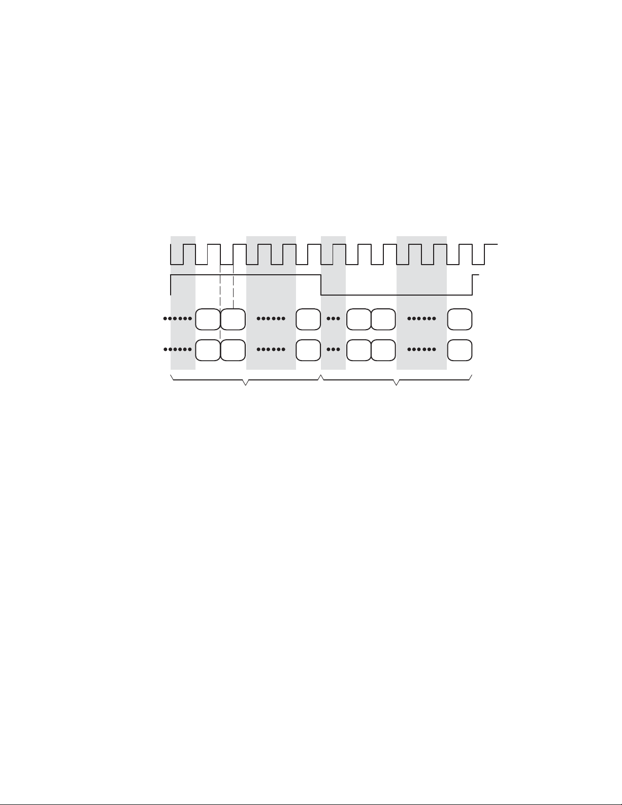
2.1.2 Left-Justified Serial Format
The following are characteristics of this protocol:
• LRCLK is the left/right clock. The left channel is transmitted when LRCLK is high. The right channel is
transmitted when LRCLK is low.
• The SDIN data is justified to the leading edge of LRCLK.
• The MSBs are transmitted at the same time as the LRCLK edge and captured at the very next rising edge
of SCLK.
• Serial data is sampled into the device on the rising edge of SCLK.
• Serial data is transmitted out of the device on the falling edge of SCLK.
• SCLK = 32 × LRCLK (32 × fs SCLK is only supported for 16-bit data) or 64 × LRCLK
• In this mode, LRCLK does not have to be a 50% duty-cycle clock. The number of bits used in the interface
sets the minimum duty cycle. There must be enough SCLK pulses to shift all of the data.
SCLK
LRCLK = f
SDIN
SDOUT
s
MSB
MSB
LSB
LSB
Left Channel Right Channel
MSB
MSB
LSB
LSB
Figure 2−3. Left-Justified Serial Format
2−3
Page 18
2.1.3 Right-Justified Serial Format
The following are characteristics of this protocol:
• LRCLK is the left/right clock. The left channel is transmitted when LRCLK is high. The right channel is
transmitted when LRCLK is low.
• The SDIN data (recorded data) is justified to the trailing edge of the LRCLK.
• Serial data is sampled on the rising edge of SCLK.
• Serial data is transmitted on the falling edge of SCLK.
• In this mode, LRCLK does not have to be a 50% duty-cycle clock. The number of bits used in the interface
sets the minimum duty cycle. There must be enough SCLK pulses to shift all of the data.
SCLK
LRCLK = f
SDIN1
SDOUT
s
MSBX
MSBX
Left Channel Right Channel
LSB
LSB
MSBX
MSBX
LSB
LSB
Figure 2−4. Right-Justified Serial Format
2.2 LRCLKOUT and SCLKOUT
The digital audio processor and on-chip logic are sequenced using an internal system clock that is derived from MCLK
(master clock). Also derived from MCLK are the LRCLKOUT and SCLKOUT signals that provide clocks to the
TAS3001 and other devices in the system.
The TAS3001 allows multiple system clocking schemes. In Figure 2−5, the TAS3001 provides system clocks (LRCLK
and SCLK) to other parts of the system. In Figure 2−6, a system master other than the TAS3001, provides system
clocks (LRCLK and SCLK) to the TAS3001.
2−4
Page 19

MCLK
Crystal
Oscillator
S/PDIF
Receiver
TAS3001
LRCLKOUT
SCLKOUT
SCLK
LRCLK
10
11
9
MCLK
LRCLK
SCLK
Figure 2−5. Master Mode
MCLK
9
MCLK
10
11
LRCLK
SCLK
TAS3001
SCLK
LRCLK
Figure 2−6. Slave Mode
23
24
TLC320AD77
(Codec)
TLC320AD77
(Codec)
2−5
Page 20

2−6
Page 21

3 Serial Control Interface (I2C)
The TAS3001 operation is controlled using the RESET signal and the serial control interface. Control information is
downloaded into the TAS3001 control registers by an I
2
C master device, such as a microprocessor, microcontroller,
or DSP. These registers control the settings for volume, bass, treble, mixing, and filtering. A description of the register
addresses and control formats is given in Appendix A.
2
The I
C bus employs two signals, SDA (data) and SCL (clock), to communicate between integrated circuits in a
system. Each device is addressed by sending a unique 7-bit slave address plus an R/W
2
C compatible devices are controlled using the SDA and SCL signals using a wire-ANDed connection. A pullup
All I
resistor must be used to set the high level on the bus. The TAS3001 operates in standard I
bit (1 byte).
2
C mode up to 100 kbps
with as many devices on the bus as desired up to the capacitance load limit of 400 pF.
2
The TAS3001 is an I
must operate in master mode. The pullup resistor is generally 4.99 kΩ. Upon power up, the I
C slave-only device; therefore, at least one device connected to the I2C bus with this device
2
C is in an unknown state
until the master clock has been applied and the T AS3001 has been reset. Prior to reset, the TAS3001 may hold the
SDA and/or SCL lines low. This creates I
2
C communication errors for any other device that attempts to use the bus.
3.1 I2C Protocol
The bus standard uses transitions on the data pin (SDA) while the clock is high to indicate start and stop conditions.
A high-to-low transition on SDA indicates a start and a low-to-high transition indicates a stop. Normal data-bit
transitions must occur within the low time of the clock period. These conditions are shown in Figure 3−1. These start
and stop conditions for the I
also generate the 7-bit slave address and the read/write (R/W
then wait for an acknowledge condition. The slave holds SDA low during acknowledge clock period to indicate an
acknowledgment. When this occurs, the master transmits the next byte of the sequence.
2
C bus are required by standard protocol to be generated by the master. The master must
) bit to open communication with another device and
After each 8-bit word, an acknowledgment must be transmitted by the receiving device. There is no limit on the
number of bytes that can be transmitted between start and stop conditions. When the last word transfers, the master
generates a stop condition to release the bus. A generic data transfer sequence is shown in Figure 3−1. Definitions
for the I
2
C protocol terms are listed in Table 3−1.
SDA
SCL
7 Bit Slave Address
76543210 76543210 76543210 76543210
Start Stop
R/W
8 Bit Subaddress (N)AA
8 Bit Data For
Address (N)
A
8 Bit Data For
Address (N)
A
Figure 3−1. Typical I2C Data Transfer Sequence
T able 3−1. I
DEFINITION DESCRIPTION
Master The device that initiates a transfer, generates clock signals, and terminates the transfer
Receiver The device that receives data
Slave The device addressed by the master
2
C Protocol Definitions
3−1
Page 22

3.2 Operation
To permit multiple devices to be controlled via the I2C bus, each slave device has an address. The TAS3001 has been
assigned four unique addresses to permit multiple TAS3001s to be used in a system. The addresses are selected
using the CS1 and CS2 pins. These four addresses, listed in Table 3−2, are licensed I
with other licensed I
2
C audio devices. To communicate with the TAS3001, the I2C master must use the address
01101XX. In addition to the 7-bit device address, subaddresses are used to direct communication to the proper
memory location within the device. A complete table of subaddresses and control registers is provided in Appendix A,
Software Interface.
Table 3−2. TAS3001 I
I2C ADDRESS BYTE A6−A2 CS2(A1) CS1(A0) R/W
68h 01101 0 0 0
6Ah 01101 0 1 0
6Ch 01101 1 0 0
6Eh 01101 1 1 0
2
C Address
3.2.1 Write Cycle Example
An example write cycle is demonstrated in Figure 3−2 and Table 3−3.
Start Slave Address R/W A Subaddress A Data Byte 1 A Data Byte 1 A Data Byte 2 A Data Byte N A Stop
Figure 3−2. Write Cycle Example
Table 3−3. Write Cycle Example
FUNCTION DESCRIPTION
Start Start condition as defined in I2C
Slave address 0110100 (CS1 = CS2 = 0)
R/W 0 (write)
A Acknowledgement as defined in I2C (slave)
Subaddress 00000110 (see Appendix A, Software Interface)
Data 00011100 (see Appendix A, Software Interface)
Stop Stop condition as defined in I2C
2
C addresses and do not conflict
Whenever writing to a subaddress, the correct number of data bytes must follow in order to complete the write cycle.
For example, if the volume control register with subaddress 04h is written to, six bytes of data must follow; otherwise,
the cycle will be incomplete and errors will occur.
3.2.2 I2C Timing and Wait Cycles
The TAS3001 issues I2C wait cycles to regulate the flow of command information. The T AS3001 can issue wait cycles
for each instruction. For any instruction, the TAS3001 can issue up to a one sample (23 µs) wait between data bytes
and between the last data byte and the I
this wait cycle is slightly longer than a sample interval, on the order of 1.1 x 1 ÷ F
cycle is illustrated in Figure 3−3.
Start Slave Address R/W A Subaddress A Data Byte 1 A Wait Data Byte 1 A Wait Data Byte 2 A Wait Data Byte N A Wait Stop
The TAS3001 can also issue an I
produces these wait cycles while it executes the interpolation algorithms from the present setting to the new setting.
The volume command always takes the same amount of time to process for a given sample rate. The treble and bass
commands vary depending upon the current index and the destination index. E.g., moving from −18 dB to 18 dB or
vice versa produces the longest wait.
3−2
2
C stop. This wait is generated after the acknowledgement. The duration of
( or 25 µs at 44.1 kHz). This wait
s
Figure 3−3. Wait Cycle Example
2
C wait state after receiving an entire volume or tone command. The TAS3001
Page 23

However, this wait cycle does not occur during the volume or tone change command, instead it occurs during the next
COMMENT
command after the acknowledgement of the first data byte.
Table 3−4 gives typical values of the wait states of the T AS3001 commands.
T able 3−4. I
SYSTEM SAMPLING FREQUENCY
32 kHz 44.1 kHz 48 kHz 96 kHz
Volume 62 ms 49 ms 41 ms 21 ms Not dependent on size of change
Bass 231 ms 167 ms 153 ms 77 ms
Treble 231 ms 167 ms 153 ms 77 ms
Mixer None None None None
Equalization None None None None
2
C Wait States
18 dB to −18 dB (proportional to step
change)
18 dB to −18 dB (proportional to step
change)
The I2C operation sequence that the TAS3001 uses to assert an I2C wait cycle is:
1. The TAS3001 detects a valid start condition and correct device ID. At this point the TAS3001 issues an ACK.
2. The TAS3001 decodes the eight-bit subaddress and issues another ACK.
3. The TAS3001 decodes the first data byte and issues a third ACK.
4. At this point, the TAS3001 device can hold the SCL clock line low until the internal controller is ready to
accept more data. This is an I
There are two ways a master can handle the I
• The preferred way to handle wait states is to use an I
wait-state period, the master stops sending data over I
2
C slave wait state.
2
C slave wait.
2
C master that recognizes wait states. During the
2
C. In this case, when the master releases the clock
to go high after a slave ACK (to latch in the next bit of data), the master monitors the SCL line and ensures
that the slave has released SCL. Once SCL has been released the master can start the next transmission.
• Alternatively, if this function is not available on the system controller, fixed delays can be implemented in
the system software to ensure that the TAS3001 is ready to receive additional data. Sending I
2
C data while
the TAS3002 device is busy causes errors and the device locks up and have to be reset.
Issuing a stop command in the middle of an I
2
C transaction puts the T AS3001 I2C slave block into an unknown state,
possibly locking up the controller or causing it to send incorrect data to the signal processing block.
3.2.3 Resetting the TAS3001 I2C Interface
To put the TAS3001 back into a known state, an I2C transaction with a subaddress of 00h and followed by 16 bytes
of zeros clears out the I
During normal operation, the TAS3001 should never issue a NACK. If the TAS3001 issues a NACK, this is an
indication of an I
2
2
C slave block buffer. Resetting the device also puts it into a known state.
C protocol discrepancy.
3.2.4 Power-Up Conditions
Upon system power up, the I2C bus SCL can initialize in a mode in which the line is held low. This prevents any I2C
operations from being performed. To prevent this from occurring, always hold RESET
low for a minimum of 10 MCLK
clock cycles after applying power.
Upon reset, the TAS3001 goes through an initialization sequence with a duration of 5 ms.
Before a reset, the SDA and SCL lines may be held low by the device.
3−3
Page 24

3.2.5 I2C Serial Port Timing
PARAMETER MIN MAX UNIT
f
(scl)
t
BUF
t
w(low)
t
w(high)
t
h(STA)
t
su(STA)
t
h(DAT)
t
su(DAT)
t
r
t
f
t
su(STO)
†
A device must internally provide a hold time of at least 300 ns for the SDA signal to bridge the undefined region of the falling edge of SCL.
NOTES: 1. t
SCL clock frequency 0 100 kHz
Bus free time between start and stop 4.7 µs
Pulse duration, SCL clock low (see Note 1) 4.7 µs
Pulse duration, SCL clock high (see Note 2) 4 µs
Hold time, repeated start 4 µs
Setup time, repeated start 4.7 20 µs
Hold time, data 0
Setup time, data 250 ns
Rise time for SDA and SCL 1000 ns
Fall time for SDA and SCL 300 ns
Setup time for stop condition 4 µs
is measured from the end of tf to the beginning of t
2. t
w(low)
is measured from the end of tr to the beginning of t
w(high)
r.
f.
†
µs
SDA
t
BUF
SCL
PS
t
h(STA)
Data Line
Valid
t
t
r
Stable
h(DAT)
Change of Data
Allowed
t
f
t
su(DAT)
Figure 3−4. I2C Serial Port Timing
t
su(STA)
t
h(STA)
t
su(STO)
P
3−4
Page 25

4 Digital Audio Processor
4.1 Input Mixer Control
The TAS3001 is capable of mixing two channels of serial audio data. The mixer permits each input to scaled (−∞ to
+18 dB) independently and then a stereo summation is performed. One important function of this circuit is to scale
the input signals down to compensate for gains in the equalization settings and the bass and treble controls. This
prevents the system from exceeding the maximum digital signal output.
The mixer operation is controlled by loading values into the MIXER1 (07h) and MIXER2 (08h) control registers. The
mixer control values are in 4.20 format—4 bits for the integer and 20 bits for the fraction. The formula for converting
a 4.N number to dB is: dB = 20 log(X), where X is a positive 4.N number. To mute a mixer channel, 0s are loaded into
its respective mixer control register.
In order to transmit mixer control values over I
nibble of byte 2 is the integer; the second nibble of byte 2 and bytes 1 and 0 are the fraction.
T able A−7 contains dB converted into 4.20 numbers for the range –70 dB to 18 dB, although any positive 4.20 number
can be used.
The mixer operation is updated instantly in response to a control register change. This may cause audible artifacts
when changing mixer settings outside of fast load mode.
4.2 Biquad Block
The biquad block consists of six digital biquad filters per channel organized in a cascade structure as shown in
Figure 4−1. Each of these biquad filters has five downloadable 24-bit (4.20) coefficients. Each stereo channel has
independent coefficients.
2
C, it is necessary to separate each value into three bytes. The first
Biquad 1 Biquad 2 Biquad N
Figure 4−1. Cascaded Biquad Filters
4.2.1 Filter Coefficients
The filter coefficients for the TAS3001 are downloaded through the I2C port and loaded into the biquad memory space.
Digital audio data coming into the device is processed by the biquad filters and then output from the device, usually
to an external DAC. Any biquad filter may be downloaded and processed by the TAS3001. The biquad structure that
is used for the parametric equalization filters is:
H(z) +
b0) b1Z–1) b2Z
1 ) a1Z–1) a2Z
The coefficients for these filters are quantized and represented in 4.20 format—4 bits for the integer part and 20 bits
for the fractional part. Each biquad uses five coefficients to define the operation.
–2
–2
4.3 Volume Control Functions
4.3.1 Soft Volume Update
The TAS3001 implements a Texas Instruments proprietary soft volume update. This update allows a smooth and
pleasant-sounding change from one volume level to another over the entire range of volume (18 dB to mute).
4−1
Page 26

The volume is adjustable by downloading a 4.20 gain coefficient through the I2C interface to register (04h). Table A−4
in the Appendix lists the 4.20 coefficient values for 0.5-dB volume steps for the range of –70 dB to 18 dB. However,
positive 4.20 values other than those listed in Table A−4 are allowed.
Right and left channel volumes can be unganged and set to different values to implement balance control.
4.3.2 Software Soft Mute
Mute is implemented by loading all zeros in the volume control register. This causes the volume to ramp down
automatically over a maximum of 2048 samples to a final output of zero (–∞ dB).
4.4 Tone Controls
4.4.1 Treble Control
The treble gain level may be adjusted within the range of 18 dB to –18 dB with 0.5 dB step resolution. The level
changes are accomplished by downloading the one byte treble control codes into the treble control register (05h).
The bass control codes are shown in Table A−5.
4.4.2 Bass Control
The bass gain level may be adjusted within the range of 18 dB to –18 dB with 0.5 dB step resolution. The level changes
are accomplished by downloading the one byte bass control codes into the bass control register (06h). The treble
control codes are shown in Table A−6.
4.4.3 Frequency Dependence of Treble and Bass Controls
The bass and treble controls are based upon fixed filter coefficients. The coefficients define a response that is a based
upon the data sample rate. As a result, if the sample rate is increased or decreased by a factor, the filter frequency
response will increase or decrease in frequency by an equal factor. Table 4−1 and Table 4−2 show the relationship
between the sample frequency and corner frequency for the bass and treble controls.
Table 4−1. Bass Control Corner Frequencies
Sampling Rate 32,000 44,100 48,000 96,000
Corner Frequency 72.6 100.0 108.8 217.7
Table 4−2. Treble Control Corner Frequencies
Sampling Rate 32,000 44,100 48,000 96,000
Corner Frequency 7,256 10,000 10,884 21,769
4−2
Page 27

5 Device Operation
5.1 Device Initialization
5.1.1 Reset
The reset pin allows the device to be reset. The reset operation is a synchronous operation requiring MCLK to perform
the sequence of reset operations. During reset, the TAS3001 returns to the default state as described in this section
and goes through the initialization process. The T AS3001 does not reset automatically when power is applied to the
device.
A reset is required after power is applied to any of the power pins.
Required conditions for a successful reset:
• MCLK is running.
• RESET
is low for a minimum of 10 MCLK cycles.
The reset operation typically takes 5 ms to complete.
Once reset has completed, the master control register (MCR) should be set. The MCR sets the serial mode and fast
load. It is recommended that the MCR be set only once, following reset.
5.1.2 Device Power On and System Reset
When power is applied to the TAS3001, the device powers up in an unknown state. It must be reset before the device
will be in a known state. It is recommended that RESET
internal reset operations in 5 ms and is then ready for operation. Following the reset, the TAS3001 initializes to its
default state (fast load mode). The main control register is configured to 1XXX XXXX, where X is not initialized, as
shown in Figure 5−1 (see Appendix A for a complete description of the MCR). Only the fast load bit set to a 1 in the
main control register. This puts the device into fast load mode (see the Initialization section). All random access
memory (RAM) will be initialized (previous data will be overwritten).
Bit 7 Bit 0
1
X X X X X X X
Figure 5−1. Main Control Register (MCR)
2
The I
C address pins (CS1 and CS2) should be driven or biased to set the TAS3001 to a known I2C address. This
also ensures the I
2
C port is active immediately after the reset initialization phase. Furthermore, when implementing
a three- or six-speaker system, the CS1 and CS2 pins must always be driven or set to unique addresses on all
devices. The I
2
C port is powered up but does not acknowledge any I2C bus activity until the entire device has been
initialized. This initialization typically takes 5 ms.
be applied following power up. The TAS3001 performs its
5.1.3 Initialization
After reset, the system enters fast-load mode and the following occur as part of initialization:
• All of the parametric EQ is initialized to 0 dB (all-pass).
• The tone (bass/treble) is set to 0 dB.
• The mix function sets SDIN1 to 0 dB and SDIN2 to mute (no-pass).
• The volume is set to mute.
5−1
Page 28

While in fast-load mode, it is possible to update the parametric EQ without any audio processing delay. The audio
N
P
processor pauses while the RAM is being updated in this mode. It is recommended that parametric EQ be
downloaded in this mode. Bass and treble cannot be downloaded in this mode. Mixer1 and Mixer2 registers can be
downloaded in this mode or normal mode (FL bit = 0). It is not recommended to download the volume control register
and mixer registers in this mode. Once the download is complete, the fast-load bit needs to be cleared by writing a
0 into bit 7 of the main control register. This puts the TAS3001 into normal mode.
NOTE: While in the fast-load mode, the TAS3001 does not accept audio. The device must be
set to the normal mode before it can accept and process audio data.
When coming out of fast-load mode, it is good practice to be sure that the system is muted. This prevents the system
from producing spurious pops and clicks. Once back in normal mode, treble, bass, and volume controls can be
downloaded to complete device setup.
5.2 Power Consumption
During normal operation the average power consumption is 20 mA.
When RESET
is held low, asserted, the TAS3001 draws an average current of 35 mA.
5.3 Power Down and Restart
The TAS3001 can be placed in a low-power mode. It is entered synchronously by asserting the POWERDOWN pin
high, logic 1, followed by asserting the RESET
down. MCLK must be present for the TAS3001 to enter the power-down mode.
pin low, logic 1, 1 µs later. Figure 5−2 illustrates the timing for power
1 µs
MCLK
RESET
POWERDOWN
OTE: RESET and POWERDOWN do not have to be synchronized with MCLK.
Figure 5−2. Power-Down Timing
To recover from the power-down state, the POWERDOWN pin is set low, logic 0, followed by asserting the RESET
pin high, logic 0, 1 µs later. Figure 5−3 illustrates the timing for start-up. MCLK must be present for the TAS3001 to
exit the power-down mode.
1 µs
MCLK
RESET
OWERDOWN
NOTE: RESET
and POWERDOWN do not have to be synchronized with MCLK.
Figure 5−3. Start-Up Timing
5−2
Page 29

6 Electrical Characteristics
DD
PLL and digital IC supply current, I
DD
mA
6.1 Absolute Maximum Ratings Over Operating Free-Air Temperature Range
(Unless Otherwise Noted)
Supply voltage range, AVDD_PLL, DVDD −0.3 V to 4.2 V. . . . . . . . . . . . . . . . . . . . . . . . . . . . . . . . . . . . . . . . . . .
Digital input voltage range −0.3 V to V
Operating free-air temperature range, T
Storage temperature range, T
Case temperature for 10 seconds, T
Lead temperature from case for 10 seconds 97.8°C. . . . . . . . . . . . . . . . . . . . . . . . . . . . . . . . . . . . . . . . . . . . . . . .
ESD tolerance
†
Stresses beyond those listed under “absolute maximum ratings” may cause permanent damage to the device. These are stress ratings only , a nd
functional operation of the device at these or any other conditions beyond those indicated under “recommended operating conditions” is not
implied. Exposure to absolute-maximum-rated conditions for extended periods may affect device reliability.
‡
Human body model per method 3015.2 of MIL-STD-883B.
‡
2000 V. . . . . . . . . . . . . . . . . . . . . . . . . . . . . . . . . . . . . . . . . . . . . . . . . . . . . . . . . . . . . . . . . . . . . . . . .
†
0°C to 70°C. . . . . . . . . . . . . . . . . . . . . . . . . . . . . . . . . . . . . . . . . . . . . .
−65°C to 150°C. . . . . . . . . . . . . . . . . . . . . . . . . . . . . . . . . . . . . . . . . . . . . . . . . .
stg
A
122.3°C. . . . . . . . . . . . . . . . . . . . . . . . . . . . . . . . . . . . . . . . . . . . . . . . . . . .
C
DD
+ 0.3 V. . . . . . . . . . . . . . . . . . . . . . . . . . . . . . . . . . . . . . . . . . . . . . . . . .
6.2 Recommended Operating Conditions
MIN NOM MAX UNIT
PLL supply voltage, AV
Digital IC supply voltage, DV
Capacitive load for each bus line C
Operating free-air temperature, T
DD
DD
(SDA, SCL) 400 pF
L(bus)
A
3 3.3 3.6 V
3 3.3 3.6 V
0 25 70 °C
6.3 Power Consumption
PARAMETER TEST CONDITIONS
PLL and digital IC supply current, I
6.4 Static Digital Specifications
PARAMETER TEST CONDITIONS MIN TYP MAX UNIT
V
V
V
V
I
IH
I
IL
I
OZ(H)
I
OZ(L)
High-level input voltage 2 VDD +0.3 V
IH
Low-level input voltage −0.3 0.8 V
IL
High-level output voltage IO = −1 mA 2.4 V
OH
Low-level output voltage IO = 4 mA 0.4 V
OL
High-level input leakage current −10 10 µA
Low-level input leakage current −10 10 µA
High-level output leakage current SCL, SDA −10 10 µA
Low-level output leakage current SCL, SDA −10 10 µA
32−48 kHz
SAMPLE
RATE
TYP TYP
VDD = 3.3 V, No load 20 40
VDD = 3.3 V, No load, Reset active 35 70
VDD = 3.3 V, No load, Standby 2 4
96 kHz
SAMPLE
RATE
DD
UNIT
mA
V
6−1
Page 30

Digital
Amplifier
Digital Amplifier Control
CS1 28
TAS3001
1 CS2
NC 26
NC 25
SCLKOUT 24
RESERVED 27
2 DVSS3 DVDD4 SDA
5 SCL
19
NC 22
NC 20
NC 21
RESET
LRCLKOUT 23
6 SDIN1
7 SDIN2
8 SDOUT
9 MCLK
10 LRCLK
Dig Gnd
NC 17
NC 18
RESERVED 15
POWERDOWN 16
_PLL
_PLL
DD
SS
11 SCLK
12 A V
13 AV
14 CAP_PLL
Serial Data Out
68 nF
27 W
Clocks
Serial Data In
S/PDIF Receiver
Dig Gnd
27 W
4.99 kW
4.99 kW
2.7 W
C Control
2
Initialization &
I
Power Down
Micro controller
3.3 V Digital
Figure 6−1. Typical TAS3001 Connection
100 nF
10 uF
100 nF
10 mF
1500 pF
Dig Gnd
Dig Gnd
Dig Gnd
6−2
Page 31

7 Measured Audio Performance for Some Typical Examples
To illustrate the performance of the TAS3001, a series of measurements was performed on a system shown in
Figure 7−1.
Measurement
System
S/PDIF
Receiver
TAS3001
Control
Interface
S/PDIF
Transmitter
TAS3001 Test System
Figure 7−1. Audio Performance Measurement System
The system performance was measured for three filter types at 48 kHz.
• Butterworth high-pass filter at 1 kHz
• Butterworth low-pass filter at 1 kHz
• EQ filter at 1 kHz with a gain of 8 dB and a bandwidth of 500 Hz
The audio performance that was measured is shown in Table 7−1. The response shapes of the three test filters are
shown in Figure 7−2.
Table 7−1. Audio Filter Performance
PARAMETER FILTER CONDITIONS MEASURED
All-pass Vol = 0, mixer –0 dB, 48-kHz f
THD+N
SNR All filters > 110 dB
IM All filters
1-kHz second-order Butterworth high- and low-pass filters Vol = 0, mixer –0 dB, 48-kHz f
1-kHz EQ +8 dB, 500-Hz bandwidth Vol = 0, mixer –8 dB, 48 kHz f
s
s
s
< −1 10 dB
< 0.0003%
< −106 dB
< 0.0005%
< −108 dB
< 0.0004%
< −98 dB
< 0.001%
7−1
Page 32

10
5
0
−5
Attenuation − dB
−10
−15
ATTENUATION
vs
FREQUENCY
−20
100 1k 10k
f − Frequency − Hz
Figure 7−2. Audio Performance Test Filters
7−2
Page 33

8 Using the TAS3001 in a System
8.1 TAS3001 Applications
The TAS3001 can be used to perform a number of audio processing functions.
The TAS3001 can be used to perform parametric equalization to correct the frequency response of a pair of
loudspeakers and microphones as shown in Figure 8−1. In this case, the TAS3001 is used to shape the frequency
response of the transducers by applying filters to compensate for the response irregularities of each transducer
(peaks and valleys of the microphone and loudspeaker response).
USB Interface
TUSB3200
or TAS1020
Streaming
USB Controller
TAS3001
TAS3001 Preamplifier
TLC320AD77
DAC Section
TLC320AD77
ADC Section
Conventional
Amplifier
Figure 8−1. TAS3001 as a System Equalizer
The filters can be developed and evaluated using a personal computer, the TAS3001 EVM, a speaker analysis
package, and the automatic loudspeaker equalization program. The next section demonstrates the use of the Texas
Instruments automatic loudspeaker equalization program that automates many of the steps in developing filters for
loudspeaker equalization.
A second application of the TAS3001 is to perform both the crossover and frequency equalization of individual
loudspeaker drivers in a two- or multi-way loudspeaker design as in Figure 8−2. In this case, the TAS3001 provides
two functions: the crossover band-pass and band-limiting functions for each speaker and the compensation for the
response irregularities of each loudspeaker driver.
8−1
Page 34

DIR1703
S/PDIF Receiver
S/PDIF Interface
% TAS3001
Digital
Amplifier
TAS5100
H − Bridge
TAS5100
PWM
Tweeter
Woofer
% TAS3001
TAS5100
H − Bridge
Figure 8−2. TAS3001 as a Crossover and Equalizer
8.2 Measurement-Based Speaker Correction
Although loudspeakers ideally should be designed for a uniform sound pressure response as a function of frequency,
cost and physical constraints usually result in speakers that are less than ideal. To correct large nonlinearities in the
response or to shape the response to listener preferences, speaker equalization can be performed.
In the example speaker response shown in Figure 8−3, it is seen that the sound pressure level (y-axis) varies
significantly as a function of frequency (x-axis). For speakers such as this typical loudspeaker, equalization can
improve performance and enhance the listening experience.
8−2
Page 35

Figure 8−3. Typical Small Loudspeaker Response
In addition to equalization of the frequency response, the TAS3001 can be used to notch out specific frequencies that
excite mechanical resonances in the speaker. The removal of mechanical resonances improves the temporal
response of the loudspeaker, so that it more accurately reproduces a recorded signal. For small and ported
loudspeakers, a high-pass filter eliminates signal energy that is lower than the speaker can reproduce. This filtering
improves the loudspeaker power handling and intelligibility by eliminating large cone excursions produced by signals
that are below the loudspeaker resonant frequency.
The kinds of corrections being discussed here begin with a thorough understanding of the inherent operation of the
particular loudspeaker. This information can best be obtained by means of a measurement such as that shown in
Figure 8−3. The measurement information allows the equalization designer to find the resonances and other
problems associated with the speaker and to correct them.
8.3 Sound-Based Speaker Correction
While a high-quality speaker measurement can be extremely valuable to the equalization designer, many good
equalization designers also rely upon their own perception of the sound from the speaker. Based upon what they
measure and hear, designers are able to design filters to achieve a specific frequency response and desired sonic
character. Digital filters can be used to provide these corrections and shape the produced sound.
8.4 Loudspeaker Equalization Example
An example of loudspeaker equalization follows. In Figure 8−3, a loudspeaker has the frequency response shown.
In Figure 8−5 the designer specifies the desired response that is the center of the three new lines. The lines above
and below the center line are the + and − tolerances. The tolerances can be adjusted.
8−3
Page 36

Figure 8−4. Preparation for Equalization
Figure 8−5 shows the corrected loudspeaker response that has been developed by the ALE program.
Figure 8−5. After Equalization
8−4
Page 37

Figure 8−6 shows the filters that were used to equalize the loudspeaker response.
Figure 8−6. Equalization Filters
8.5 Speaker Correction and Equalization
Digital filters are able to provide a fairly broad range of filter types and responses.
The TAS3001 contains six programmable filters. The system designer has the choice of using one to all six of these
filters. The filters can be used to equalize response peaks and dips from a desired response. They can also be used
to shape the loudspeaker phase response. Because of their available precision and temperature insensitivity, not only
can the filters be used to equalize the frequency and phase response of a loudspeaker closely, but they also can be
used to remove resonances or other small deviations in the response of a loudspeaker surgically. This permits the
system designer a greater degree of flexibility in the design of both the individual loudspeaker drivers and the cabinet.
If additional filtering is needed, multiple TAS3001s can be cascaded.
This enables greater freedom in the design of acoustical systems. The TAS3001 permits additional flexibility in
transducer design. Overall flatness of a transducer response is no longer an overriding concern with the
low-cost/high-performance frequency correction of the TAS3001. The constraints on the transducer design can be
relaxed so that they provide optimum performance after correction. This, in turn, allows the transducer and its
equalization to be designed as a system, providing wide flexibility in the design and achieving outstanding sound
presentation.
8.6 The TAS3001 Can Implement Nearly Any Second-Order IIR Filter
Filter designs can tax computational resources, so it is not uncommon to see simplified filter implementations that
must limit either the number of or the nature of the filters that can be implemented. For example, a particular
architecture might impose limits on the gains, Qs, and/or center frequencies that can be implemented. This, however ,
is not the case with the TAS3001. Its high-precision, patent-pending structure allows implementation of almost any
second-order IIR filter. These are implemented in an almost limitless range of filter functions without fear of
degradation due to limit cycles or increased system noise.
Additionally, higher order filters can be developed by factoring the desired filter into consecutive multiple
second-order sections. Similarly, any filter that has been designed in analog can be converted and implemented as
a digital filter.
8−5
Page 38

10
5
0
Attenuation − dB
−5
ATTENUATION
vs
FREQUENCY
−10
100 1k 10k
f − Frequency − Hz
Figure 8−7. Individual Filters
From left to right the filters that are shown in Figure 8−7 are:
• Variable Q high-pass filter with a Q = 1.3 to emphasize the bass and prevent distortion by cutting of
frequencies below the cabinet resonance
• Equalization filters of various amplitudes, center frequencies, and bandwidths
• A treble shelf
• A Chebychev low-pass filter with a ripple of 1 dB to attenuate high frequencies
The combined response of these filters is shown in Figure 8−8.
ATTENUATION
vs
10
5
0
FREQUENCY
8−6
Attenuation − dB
−5
−10
100 1k 10k
f − Frequency − Hz
Figure 8−8. Combined Response
Page 39

8.7 Converting Analog Filters to Digital
Many audio engineers may already be using analog equalization. If a satisfactory set of analog filters has already
been defined, the user can convert those analog filters to digital. This is perhaps the easiest way to get started. For
converting analog filters to digital, refer to Digital Signal Processing, A. V. Oppenheim, R. W. Schafer, Prentice-Hall,
1975, pp. 197–211. This information is also available in almost any digital signal processing textbook. Users of Matlab
can perform these manipulations easily using the BILINEAR or IMPINVAR commands available in the Matlab signal
processing toolbox.
8−7
Page 40

8−8
Page 41

9 Automatic Loudspeaker Equalizer
To simplify the process of designing digital filters for implementation in the T AS3001, Texas Instruments provides a
filter design tool called the Automatic Loudspeaker Equalizer or ALE. Details of this tool are provided in this section.
9.1 Automatic Generation of Equalization Filters Given a Measurement
ALE has the capability of reading in a speaker or environment measurement. The user can then provide the desired
speaker response. From these two inputs, ALE can automatically produce an optimized set of filters to equalize the
speaker. T h e p a t ent-pending optimization algorithm was developed at Texas Instruments. An example of its operation
is shown in Figure 8−3 through Figure 8−6.
9.2 Automatic Approximation of an Equalization Curve
When the desired equalization transfer function is known, the problem becomes one of finding a set of digital
second-order IIR filters to implement it. In the case where H(s) is known, it can be converted to a digital filter using
a bilinear or impulse invariant method. The resulting transfer function (H(z) can then be factored and implemented
as a combination of second- and first-order sections using the TAS3001. (This factoring capability is not included in
ALE, but can be accomplished simply in Matlab.) However, in many cases the desired transfer function can be
specified as a curve. In this case, the curve can be read by ALE. Then an approximation to it can be generated
manually (see the Manual Filter Generation section below) or automatically. In the automatic mode, ALE again uses
the patent-pending optimization technique developed at Texas Instruments.
9.3 Manual Filter Design
In many cases, the user already has filter specifications and just needs a way of designing such filters. In such cases,
ordinary filter parameters, such as gain, bandwidth, and center frequency can be entered into ALE, which then
provides coefficients for the desired filters. As filters are generated, ALE displays the responses of individual filters
and the composite filter response. In addition, the manual filter generation capability can be used in conjunction with
the automatic capability (see Section 9.2, Automatic Approximation of an Equalization Curve). The user can specify
filters manually and allow ALE to optimize them and generate additional filters automatically as needed. The user
can also specify manual filters and let ALE automatically generate additional filters as needed but without disturbing
the manually-generated filters. In addition, the user can manually modify the filters created by ALE. A graphical user
interface allows easy manipulation of filters and movement between automatic and manual filter generation modes.
9.4 Conversion of Decimal Filter Coefficients to the TAS3001 Format
The filters generated in ALE can be saved in the TAS3001 hexadecimal format (4 integer bits, 20 fraction bits, 2’s
complement). ALE can read in filters in decimal and convert them to the hexadecimal format needed for
implementation in the TAS3001.
9.5 Editing of TAS3001 File Format
ALE can read and write filter files in the TAS3001 format. This allows the filters generated to be stored in the format
used by the TAS3001 control software. In addition, ALE can read TAS3001 filter files and display the filters.
9.6 Examples of the Filter Types Available From ALE 2.1
At the current time the following filter types can be designed by ALE:
Equalization (bell-shaped) filters with a variety of center frequencies (Qs) and gains, as shown in Figure 9−1.
9−1
Page 42

Figure 9−1. Equalization Filters
Similarly, the system can design a variety of high- and low-pass filters such as Butterworth, Linkwitz-Riley, and Type 1
Chebychev. Examples of Butterworth, Linkwitz-Riley, high- and low-pass filters with equal cut frequencies (and a
pass-band ripple specification of 1 dB for the Chebychev filters), are shown in Figure 9−2.
9−2
Figure 9−2. High- and Low-Pass Filters
Page 43

Treble and bass shelf filters can be employed with various gains and corner frequencies as shown in Figure 9−3.
Figure 9−3. Treble and Bass Shelf Filters
Notch filters can be employed to remove energy that excites mechanical resonances in loudspeakers as shown in
Figure 9−4.
Figure 9−4. Notch Filters
ALE 3.2 also supports a number of filters which are not shown here, including Chebychev I, high/low plateau,
Linkwitz-Riley, and variable Q. As new versions of ALE are developed, more filter types will be added. In addition,
Texas Instruments filtering engineers are available to help TAS3001 users design any needed filter type.
9−3
Page 44

9−4
Page 45

10 FilterBuilder and FilterMaker
To make filter creation as simple as possible for everyone, Texas Instruments can provide two tools in addition to ALE
(previous section). FilterBuilder is an Excel spreadsheet based manual filter creation tool. While not nearly as capable
as ALE, it is a simple and effective way to get started quickly with filter creation.
FilterMaker is another manual filter creation tool created by Texas Instruments. It runs in the Matlab environment. This
might be the choice of those who prefer to work in Matlab or who would like to add additional capabilities to their filter
generation tool. In addition, Texas Instruments engineers can add additional filter types in either one of these two
tools.
10−1
Page 46

10−2
Page 47

Appendix A
Software Interface
T able A−1. Register Map
REGISTER ADDRESS
Reserved 00h
MCR 01h 1 C(7−0)
Reserved 02h 2 Reserved
Reserved 03h
†
Volume
Treble 05h 1 T(7−0)
Bass 06h 1 B(7−0)
‡
Mixer 1
‡
Mixer 2
Reserved 09h
Left
Biquad 0
Left
Biquad 1
Left
Biquad 2
Left
Biquad 3
Left
Biquad 4
Left
Biquad 5
Reserved 10h−12h
Right
Biquad 0
Right
Biquad 1
Right
Biquad 2
Right
Biquad 3
Right
Biquad 4
Right
Biquad 5
Reserved 19h−FFh
†
‡
‡
‡
‡
‡
‡
‡
‡
‡
‡
‡
‡
The volume value is a 4.16 coefficient. In order to transmit it over I2C, it is necessary to separate the value into three bytes. Byte 2 (MSB) is the
integer part and bytes 1 and 0 are the fractional part.
The mixer gain values and biquad coefficients are 4.20 coefficients. In order to transmit them over I2C, it is necessary to separate the value into
three bytes. The first nibble of byte 2 (MSB) is the integer part; the second nibble of byte 2 and bytes 1 and 0 are the fractional part.
04h 6 VL(23−16), VL(15−8), VL(7−0), VR(23−16), VR(15−8), VR(7−0)
07h 3 S(23−16), S(15−8), S(7−0)
08h 3 S(23−16), S(15−8), S(7−0)
0Ah 15 B0(23−16), B0(15−8), B0(7−0), B1(23−16), B1(15−8), B1(7−0), B2(23−16), B2(15−8), B2(7−0),
0Bh 15 B0(23−16), B0(15−8), B0(7−0), B1(23−16), B1(15−8), B1(7−0), B2(23−16), B2(15−8), B2(7−0),
0Ch 15 B0(23−16), B0(15−8), B0(7−0), B1(23−16), B1(15−8), B1(7−0), B2(23−16), B2(15−8), B2(7−0),
0Dh 15 B0(23−16), B0(15−8), B0(7−0), B1(23−16), B1(15−8), B1(7−0), B2(23−16), B2(15−8), B2(7−0),
0Eh 15 B0(23−16), B0(15−8), B0(7−0), B1(23−16), B1(15−8), B1(7−0), B2(23−16), B2(15−8), B2(7−0),
0Fh 15 B0(23−16), B0(15−8), B0(7−0), B1(23−16), B1(15−8), B1(7−0), B2(23−16), B2(15−8), B2(7−0),
13h 15 B0(23−16), B0(15−8), B0(7−0), B1(23−16), B1(15−8), B1(7−0), B2(23−16), B2(15−8), B2(7−0),
14h 15 B0(23−16), B0(15−8), B0(7−0), B1(23−16), B1(15−8), B1(7−0), B2(23−16), B2(15−8), B2(7−0),
15h 15 B0(23−16), B0(15−8), B0(7−0), B1(23−16), B1(15−8), B1(7−0), B2(23−16), B2(15−8), B2(7−0),
16h 15 B0(23−16), B0(15−8), B0(7−0), B1(23−16), B1(15−8), B1(7−0), B2(23−16), B2(15−8), B2(7−0),
17h 15 B0(23−16), B0(15−8), B0(7−0), B1(23−16), B1(15−8), B1(7−0), B2(23−16), B2(15−8), B2(7−0),
18h 15 B0(23−16), B0(15−8), B0(7−0), B1(23−16), B1(15−8), B1(7−0), B2(23−16), B2(15−8), B2(7−0),
NO. OF
BYTES
BYTE DESCRIPTION
A1(23−16), A1(15−8), A1(7−0), A2(23−16), A2(15−8), A2(7−0)
A1(23−16), A1(15−8), A1(7−0), A2(23−16), A2(15−8), A2(7−0)
A1(23−16), A1(15−8), A1(7−0), A2(23−16), A2(15−8), A2(7−0)
A1(23−16), A1(15−8), A1(7−0), A2(23−16), A2(15−8), A2(7−0)
A1(23−16), A1(15−8), A1(7−0), A2(23−16), A2(15−8), A2(7−0)
A1(23−16), A1(15−8), A1(7−0) A2(23−16), A2(15−8), A2(7−0)
A1(23−16), A1(15−8), A1(7−0), A2(23−16), A2(15−8), A2(7−0)
A1(23−16), A1(15−8), A1(7−0), A2(23−16), A2(15−8), A2(7−0)
A1(23−16), A1(15−8), A1(7−0), A2(23−16), A2(15−8), A2(7−0)
A1(23−16), A1(15−8), A1(7−0), A2(23−16), A2(15−8), A2(7−0)
A1(23−16), A1(15−8), A1(7−0), A2(23−16), A2(15−8), A2(7−0)
A1(23−16), A1(15−8), A1(7−0), A2(23−16), A2(15−8), A2(7−0)
A−1
Page 48

A.1 Main Control Register (MCR)
C(7)FLFast load
C(6)SCSCLK frequency
C(5,4)
E(1,0)
Output serial port mode
C(3,2)
F(1,0)
Input serial port mode
C(1,0)
W(1,0)
Serial port word length
Configuration of the digital serial audio interface is set up through the main control register as shown in Table A−2
and Table A−3. Bits F0 and F1 allow selection between three different serial data formats (left justified = 00, right
justified = 01, and I
as the input serial port mode set by F0 and F1. Bits W0 and W1 allow selection between three different word widths
(16-bit word = 00, 18-bit word = 01, and 20-bit word = 10). The SC bit selects 32f
bit is primarily for use during initialization and is defined in Device Initialization (see Section 5.1). See Section 3, Serial
Control Interface, for additional information on how to address the main control register.
2
S standard = 10). The output serial port mode set by E0 and E1 must be set to the same value
(0) or 64fs (1) bit clock. The FL
s
Table A−2. Main Control Register (MCR)
C7 C6 C5 C4 C3 C2 C1 C0
FL SC E1 E0 F1 F0 W1 W0
1 x x x x x x x
Table A−3. Main Control Register (MCR) Description
BIT DESCRIPTOR FUNCTION VALUE FUNCTION
C(7) FL Fast load
C(6) SC SCLK frequency
C(5,4) E(1,0) Output serial port mode
C(3,2) F(1,0) Input serial port mode
C(1,0) W(1,0) Serial port word length
0 Normal operating mode
1 (default) Fast load mode
0 SCLK = 32 × f
1 SCLK = 64 × f
00 Left justified
01 Right justified
10 I2S
11 Reserved
00 Left justified
01 Right justified
10 I2S
11 Reserved
00 16 bit
01 18 bit
10 20 bit
11 Reserved
s
s
A−2
Page 49

Table A−4. Volume Gain Values
[The gain error is less than 0.12 dB (excluding mute)]
GAIN
(dB)
18.0 07, F1, 7B
17.5 07, 7F, BB −0.5 00, F1, AE −18.5 00, 1E, 6D −36.5 00, 03, D5 −54.5 00, 00, 7B
17.0 07, 14, 57 −1.0 00, E4, 29 −19.0 00, 1C, B9 −37.0 00, 03, 9E −55.0 00, 00, 75
16.5 06, AE, F6 −1.5 00, D7, 66 −19.5 00, 1B, 1E −37.5 00, 03, 6A −55.5 00, 00, 6E
16.0 06, 4F, 40 −2.0 00, CB, 59 −20.0 00, 19, 9A −38.0 00, 03, 39 −56.0 00, 00, 68
15.5 05, F4, E5 −2.5 00, BF, F9 −20.5 00, 18, 2B −38.5 00, 03, 0B −56.5 00, 00, 62
15.0 05, 9F, 98 −3.0 00, B5, 3C −21.0 00, 16, D1 −39.0 00, 02, DF −57.0 00, 00, 5D
14.5 05, 4F, 10 −3.5 00, AB, 19 −21.5 00, 15, 8A −39.5 00, 02, B6 −57.5 00, 00, 57
14.0 05, 03, 0A −4.0 00, A1, 86 −22.0 00, 14, 56 −40.0 00, 02, 8F −58.0 00, 00, 53
13.5 04, BB, 44 −4.5 00, 98, 7D −22.5 00, 13, 33 −40.5 00, 02, 6B −58.5 00, 00, 4E
13.0 04, 77, 83 −5.0 00, 8F, F6 −23.0 00, 12, 20 −41.0 00, 02, 48 −59.0 00, 00, 4A
12.5 04, 37, 8B −5.5 00, 87, E8 −23.5 00, 11, 1C −41.5 00, 02, 27 −59.5 00, 00, 45
12.0 03, FB, 28 −6.0 00, 80, 4E −24.0 00, 10, 27 −42.0 00, 02, 09 −60.0 00, 00, 42
11.5 03, C2, 25 −6.5 00, 79, 20 −24.5 00, 0F, 40 −42.5 00, 01, EB −60.5 00, 00, 3E
11.0 03, 8C, 53 −7.0 00, 72, 5A −25.0 00, 0E, 65 −43.0 00, 01, D0 −61.0 00, 00, 3A
10.5 03, 59, 83 −7.5 00, 6B, F4 −25.5 00, 0D, 97 −43.5 00, 01, B6 −61.5 00, 00, 37
10.0 03, 29, 8B −8.0 00, 65, EA −26.0 00, 0C, D5 −44.0 00, 01, 9E −62.0 00, 00, 34
VOLUME
V(23−16),
V(15−8),
V(7−0)
9.5 02, FC, 42 −8.5 00, 60, 37 −26.5 00, 0C, 1D −44.5 00, 01, 86 −62.5 00, 00, 31
9.0 02, D1, 82 −9.0 00, 5A, D5 −27.0 00, 0B, 6F −45.0 00, 01, 71 −63.0 00, 00, 2E
8.5 02, A9, 25 −9.5 00, 55, C0 −27.5 00, 0A, CC −45.5 00, 01, 5C −63.5 00, 00, 2C
8.0 02, 83, 0B −10.0 00, 50, F4 −28.0 00, 0A, 31 −46.0 00, 01, 48 −64.0 00, 00, 29
7.5 02, 5F, 12 −10.5 00, 4C, 6D −28.5 00, 09, 9F −46.5 00, 01, 36 −64.5 00, 00, 27
7.0 02, 3D, 1D −11.0 00, 48, 27 −29.0 00, 09, 15 −47.0 00, 01, 25 −65.0 00, 00, 25
6.5 02, 1D, 0E −11.5 00, 44, 1D −29.5 00, 08, 93 −47.5 00, 01, 14 −65.5 00, 00, 23
6.0 01, FE, CA −12.0 00, 40, 4E −30.0 00, 08, 18 −48.0 00, 01, 05 −66.0 00, 00, 21
5.5 01, E2, 37 −12.5 00, 3C, B5 −30.5 00, 07, A5 −48.5 00, 00, F6 −66.5 00, 00, 1F
5.0 01, C7, 3D −13.0 00, 39, 50 −31.0 00, 07, 37 −49.0 00, 00, E9 −67.0 00, 00, 1D
4.5 01, AD, C6 −13.5 00, 36, 1B −31.5 00, 06, D0 −49.5 00, 00, DC −67.5 00, 00, 1C
4.0 01, 95, BC −14.0 00, 33, 14 −32.0 00, 06, 6E −50.0 00, 00, CF −68.0 00, 00, 1A
3.5 01, 7F, 09 −14.5 00, 30, 39 −32.5 00, 06, 12 −50.5 00, 00, C4 −68.5 00, 00, 19
3.0 01, 69, 9C −15.0 00, 2D, 86 −33.0 00, 05, BB −51.0 00, 00, B9 −69.0 00, 00, 17
2.5 01, 55, 62 −15.5 00, 2A, FA −33.5 00, 05, 69 −51.5 00, 00, AE −69.5 00, 00, 16
2.0 01, 42, 49 −16.0 00, 28, 93 −34.0 00, 05, 1C −52.0 00, 00, A5 −70.0 00, 00, 15
1.5 01, 30, 42 −16.5 00, 26, 4E −34.5 00, 04, D2 −52.5 00, 00, 9B Mute 00, 00, 00
1.0 01, 1F, 3D −17.0 00, 24, 29 −35.0 00, 04, 8D −53.0 00, 00, 93
0.5 01, 0F, 2B −17.5 00, 22, 23 −35.5 00, 04, 4C −53.5 00, 00, 8B
GAIN
(dB)
VOLUME
V(23−16),
V(15−8),
V(7−0)
0.0 01, 00, 00 −18.0 00, 20, 3A −36.0 00, 04, 0F −54.0 00, 00, 83
GAIN
(dB)
VOLUME
V(23−16),
V(15−8),
V(7−0)
GAIN
(dB)
VOLUME
V(23−16),
V(15−8),
V(7−0)
GAIN
(dB)
VOLUME
V(23−16),
V(15−8),
V(7−0)
A−3
Page 50

Table A−5. Treble Control Register
(Both left and right channel will be given the same treble gain setting)
Gain
(dB)
18.0 01h
17.5 09h 10.0 4Fh 2.5 6Ch −5.0 7Ch −12.5 8Bh
17.0 10h 9.5 52h 2.0 6Dh −5.5 7Dh −13.0 8Ch
16.5 16h 9.0 55h 1.5 6Eh −6.0 7Eh −13.5 8Dh
16.0 1Ch 8.5 57h 1.0 70h −6.5 7Fh −14.0 8Eh
15.5 22h 8.0 5Ah 0.5 71h −7.0 80h −14.5 8Fh
15.0 28h 7.5 5Ch 0.0 72h −7.5 81h −15.0 90h
14.5 2Dh 7.0 5Eh −0.5 73h −8.0 82h −15.5 91h
14.0 32h 6.5 60h −1.0 74h −8.5 83h −16.0 92h
13.5 36h 6.0 62h −1.5 75h −9.0 84h −16.5 93h
13.0 3Ah 5.5 63h −2.0 76h −9.5 85h −17.0 94h
12.5 3Eh 5.0 65h −2.5 77h −10.0 86h −17.5 95h
12.0 42h 4.5 66h −3.0 78h −10.5 87h −18.0 96h
11.5 45h 4.0 68h −3.5 79h −11.0 88h
11.0 49h 3.5 69h −4.0 7Ah −11.5 89h
T(7−0)
(hex)
Gain
(dB)
10.5 4Ch 3.0 6Bh −4.5 7Bh −12.0 8Ah
T(7−0)
(hex)
Gain
(dB)
T(7−0)
(hex)
Gain
(dB)
T(7−0)
(hex)
Gain
(dB)
T(7−0)
(hex)
Table A−6. Bass Control Register
(Both left and right channel will be given the same bass setting)
Gain
(dB)
18.0 01h
17.5 03h 10.0 1Ch 2.5 36h −5.0 53h −12.5 6Dh
17.0 06h 9.5 1Fh 2.0 38h −5.5 54h −13.0 6Eh
16.5 08h 9.0 21h 1.5 39h −6.0 55h −13.5 70h
16.0 0Ah 8.5 23h 1.0 3Bh −6.5 56h −14.0 72h
15.5 0Bh 8.0 25h 0.5 3Ch −7.0 58h −14.5 74h
15.0 0Dh 7.5 26h 0.0 3E −7.5 59h −15.0 76h
14.5 0Fh 7.0 28h −0.5 40h −8.0 5Ah −15.5 78h
14.0 10h 6.5 29h −1.0 42h −8.5 5Ch −16.0 7Ah
13.5 12h 6.0 2Bh −1.5 44h −9.0 5Dh −16.5 7Dh
13.0 13h 5.5 2Ch −2.0 46h −9.5 5Fh −17.0 7Fh
12.5 14h 5.0 2Eh −2.5 49h −10.0 61h −17.5 82h
12.0 16h 4.5 30h −3.0 4Bh −10.5 64h −18.0 86h
11.5 17h 4.0 31h −3.5 4Dh −11.0 66h
11.0 18h 3.5 33h −4.0 4Fh −11.5 69h
B(7−0)
(hex)
Gain
(dB)
10.5 19h 3.0 35h −4.5 51h −12.0 6Bh
B(7−0)
(hex)
Gain
(dB)
B(7−0)
(hex)
Gain
(dB)
B(7−0)
(hex)
Gain
(dB)
B(7−0)
(hex)
A−4
Page 51

Table A−7. Mixer1 and Mixer2 Gain Values
[The gain error is less than 0.12 dB (excluding mute)]
Gain
(dB)
18.0 7F, 17, AF
17.5 77, FB, AA −0.5 0F, 1A, DF −18.5 01, E6, CF −36.5 00, 3D, 49 −54.5 00, 07, B7
17.0 71, 45, 75 −1.0 0E, 42, 90 −19.0 01, CB, 94 −37.0 00, 39, DB −55.0 00, 07, 48
16.5 6A, EF, 5D −1.5 0D, 76, 5A −19.5 01, B1, DE −37.5 00, 36, 9E −55.5 00, 06, E0
16.0 64, F4, 03 −2.0 0C, B5, 91 −20.0 01, 99, 99 −38.0 00, 33, 90 −56.0 00, 06, 7D
15.5 5F, 4E, 52 −2.5 0B, FF, 91 −20.5 01, 82, AF −38.5 00, 30, AE −56.5 00, 06, 20
15.0 59, F9, 80 −3.0 0B, 53, BE −21.0 01, 6D, 0E −39.0 00, 2D, F5 −57.0 00, 05, C9
14.5 54, F1, 06 −3.5 0A, B1, 89 −21.5 01, 58, A2 −39.5 00, 2B, 63 −57.5 00, 05, 76
14.0 50, 30, A1 −4.0 0A, 18, 66 −22.0 01, 45, 5B −40.0 00, 28, F5 −58.0 00, 05, 28
13.5 4B, B4, 46 −4.5 09, 87, D5 −22.5 01, 33, 28 −40.5 00, 26, AB −58.5 00, 04, DE
13.0 47, 78, 28 −5.0 08, FF, 59 −23.0 01, 21, F9 −41.0 00, 24, 81 −59.0 00, 04, 98
12.5 43, 78, B0 −5.5 08, 7E, 80 −23.5 01, 11, C0 −41.5 00, 22, 76 −59.5 00, 04, 56
12.0 3F, B2, 78 −6.0 08, 04, DC −24.0 01, 02, 70 −42.0 00, 20, 89 −60.0 00, 04, 18
11.5 3C, 22, 4C −6.5 07, 92, 07 −24.5 00, F3, FB −42.5 00, 1E, B7 −60.5 00, 03, DD
11.0 38, C5, 28 −7.0 07, 25, 9D −25.0 00, E6, 55 −43.0 00, 1C, FF −61.0 00, 03, A6
10.5 35, 98, 2F −7.5 06, BF, 44 −25.5 00, D9, 73 −43.5 00, 1B, 60 −61.5 00, 03, 72
10.0 32, 98, B0 −8.0 06, 5E, A5 −26.0 00, CD, 49 −44.0 00, 19, D8 −62.0 00, 03, 40
9.5 2F, C4, 20 −8.5 06, 03, 6E −26.5 00, C1, CD −44.5 00, 18, 65 −62.5 00, 03, 12
9.0 2D, 18, 18 −9.0 05, AD, 50 −27.0 00, B6, F6 −45.0 00, 17, 08 −63.0 00, 02, E6
8.5 2A, 92, 54 −9.5 05, 5C, 04 −27.5 00, AC, BA −45.5 00, 15, BE −63.5 00, 02, BC
8.0 28, 30, AF −10.0 05, 0F, 44 −28.0 00, A3, 10 −46.0 00, 14, 87 −64.0 00, 02, 95
7.5 25, F1, 25 −10.5 04, C6, D0 −28.5 00, 99, F1 −46.5 00, 13, 61 −64.5 00, 02, 70
7.0 23, D1, CD −11.0 04, 82, 68 −29.0 00, 91, 54 −47.0 00, 12, 4B −65.0 00, 02, 4D
6.5 21, D0, D9 −11.5 04, 41, D5 −29.5 00, 89, 33 −47.5 00, 1 1, 45 −65.5 00, 02, 2C
6.0 1F, EC, 98 −12.0 04, 04, DE −30.0 00, 81, 86 −48.0 00, 10, 4E −66.0 00, 02, 0D
5.5 1E, 23, 6D −12.5 03, CB, 50 −30.5 00, 7A, 48 −48.5 00, 0F, 64 −66.5 00, 01, F0
5.0 1C, 73, D5 −13.0 03, 94, FA −31.0 00, 73, 70 −49.0 00, 0E, 88 −67.0 00, 01, D4
4.5 1A, DC, 61 −13.5 03, 61, AF −31.5 00, 6C, FB −49.5 00, 0D, B8 −67.5 00, 01, BA
4.0 19, 5B, B8 −14.0 03, 31, 42 −32.0 00, 66, E3 −50.0 00, 0C, F3 −68.0 00, 01, A1
3.5 17, F0, 94 −14.5 03, 03, 8A −32.5 00, 61, 21 −50.5 00, 0C, 3A −68.5 00, 01, 8A
3.0 16, 99, C0 −15.0 02, D8, 62 −33.0 00, 5B, B2 −51.0 00, 0B, 8B −69.0 00, 01, 74
2.5 15, 56, 1A −15.5 02, AF, A3 −33.5 00, 56, 91 −51.5 00, 0A, E5 −69.5 00, 01, 5F
2.0 14, 24, 8E −16.0 02, 89, 2C −34.0 00, 51, B9 −52.0 00, 0A, 49 −70.0 00, 01, 4B
1.5 13, 04, 1A −16.5 02, 64, DB −34.5 00, 4D, 27 −52.5 00, 09, B6 Mute 00, 00, 00
1.0 11, F3, C9 −17.0 02, 42, 93 −35.0 00, 48, D6 −53.0 00, 09, 2B
0.5 10, F2, B4 −17.5 02, 22, 35 −35.5 00, 44, C3 −53.5 00, 08, A8
Gain
S(23−16),
S(15−8),
S(7−0)
Gain
(dB)
0.0 10, 00, 00 −18.0 02, 03, A7 −36.0 00, 40, EA −54.0 00, 08, 2C
Gain
S(23−16),
S(15−8),
S(7−0)
Gain
(dB)
Gain
S(23−16),
S(15−8),
S(7−0)
Gain
(dB)
Gain
S(23−16),
S(15−8),
S(7−0)
Gain
(dB)
Gain
S(23−16),
S(15−8),
S(7−0)
A−5
Page 52

A−6
Page 53

Appendix B
Mechanical Information
PW (R-PDSO-G**) PLASTIC SMALL-OUTLINE PACKAGE
14 PINS SHOWN
0,65
1,20 MAX
14
0,30
0,19
8
4,50
4,30
PINS **
7
Seating Plane
0,15
0,05
8
1
A
DIM
6,60
6,20
14
0,10
M
0,10
0,15 NOM
0°−ā 8°
2016
Gage Plane
24
0,25
0,75
0,50
28
A MAX
A MIN
NOTES: A. All linear dimensions are in millimeters.
B. This drawing is subject to change without notice.
C. Body dimensions do not include mold flash or protrusion not to exceed 0,15.
D. Falls within JEDEC MO-153
3,10
2,90
5,10
4,90
5,10
4,90
6,60
6,40
7,90
7,70
9,80
9,60
4040064/F 01/97
B−1
Page 54

B−2
Page 55

PACKAGE OPTION ADDENDUM
www.ti.com
18-Feb-2005
PACKAGING INFORMATION
Orderable Device Status
(1)
Package
Type
Package
Drawing
Pins Package
Qty
Eco Plan
TAS3001CPW NRND TSSOP PW 28 50 None CU NIPDAU Level-2-220C-1 YEAR
TAS3001CPWR NRND TSSOP PW 28 2000 None CU NIPDAU Level-2-220C-1 YEAR
(1)
The marketing status values are defined as follows:
ACTIVE: Product device recommended for new designs.
LIFEBUY: TI has announced that the device will be discontinued, and a lifetime-buy period is in effect.
NRND: Not recommended for new designs. Device is in production to support existing customers, but TI does not recommend using this part in
a new design.
PREVIEW: Device has been announced but is not in production. Samples may or may not be available.
OBSOLETE: TI has discontinued the production of the device.
(2)
Eco Plan - May not be currently available - please check http://www.ti.com/productcontent for the latest availability information and additional
product content details.
None: Not yet available Lead (Pb-Free).
Pb-Free (RoHS): TI's terms "Lead-Free" or "Pb-Free" mean semiconductor products that are compatible with the current RoHS requirements
for all 6 substances, including the requirement that lead not exceed 0.1% by weight in homogeneous materials. Where designed to be soldered
at high temperatures, TI Pb-Free products are suitable for use in specified lead-free processes.
Green (RoHS & no Sb/Br): TI defines "Green" to mean "Pb-Free" and in addition, uses package materials that do not contain halogens,
including bromine (Br) or antimony (Sb) above 0.1% of total product weight.
(3)
MSL, Peak Temp. -- The Moisture Sensitivity Level rating according to the JEDECindustry standard classifications, and peak solder
temperature.
(2)
Lead/Ball Finish MSL Peak Temp
(3)
Important Information and Disclaimer:The information provided on this page represents TI's knowledge and belief as of the date that it is
provided. TI bases its knowledge and belief on information provided by third parties, and makes no representation or warranty as to the
accuracy of such information. Efforts are underway to better integrate information from third parties. TI has taken and continues to take
reasonable steps to provide representative and accurate information but may not have conducted destructive testing or chemical analysis on
incoming materials and chemicals. TI and TI suppliers consider certain information to be proprietary, and thus CAS numbers and other limited
information may not be available for release.
In no event shall TI's liability arising out of such information exceed the total purchase price of the TI part(s) at issue in this document sold by TI
to Customer on an annual basis.
Addendum-Page 1
Page 56

MECHANICAL DATA
MTSS001C – JANUARY 1995 – REVISED FEBRUARY 1999
PW (R-PDSO-G**) PLASTIC SMALL-OUTLINE PACKAGE
14 PINS SHOWN
0,65
1,20 MAX
14
0,30
0,19
8
4,50
4,30
PINS **
7
Seating Plane
0,15
0,05
8
1
A
DIM
6,60
6,20
14
0,10
M
0,10
0,15 NOM
0°–8°
2016
Gage Plane
24
0,25
0,75
0,50
28
A MAX
A MIN
NOTES: A. All linear dimensions are in millimeters.
B. This drawing is subject to change without notice.
C. Body dimensions do not include mold flash or protrusion not to exceed 0,15.
D. Falls within JEDEC MO-153
3,10
2,90
5,10
4,90
5,10
4,90
6,60
6,40
7,90
7,70
9,80
9,60
4040064/F 01/97
POST OFFICE BOX 655303 • DALLAS, TEXAS 75265
Page 57

WWW.ALLDATASHEET.COM
Copyright © Each Manufacturing Company.
All Datasheets cannot be modified without permission.
This datasheet has been download from :
www.AllDataSheet.com
100% Free DataSheet Search Site.
Free Download.
No Register.
Fast Search System.
www.AllDataSheet.com
 Loading...