

Page 1

User's Guide
SLOU497–October 2017
TAS2770 Stereo Evaluation Module
This user’s guide describes the characteristics, operation, and use of the TAS2770EVM-STEREO
Reference Board. A complete schematic diagram, printed-circuit board layouts, and bill of materials are
included in this document.
Contents
1 Description ................................................................................................................... 2
2 Specifications ................................................................................................................ 2
3 Software ...................................................................................................................... 2
4 Stereo Setup ................................................................................................................. 2
5 Mono Setup .................................................................................................................. 4
6 Multi-Channel Setup ........................................................................................................ 5
7 Digital Audio Interfaces ..................................................................................................... 6
8 Hardware Documentation .................................................................................................. 9
List of Figures
1 TAS2770EVM-STEREO Stereo Configuration .......................................................................... 3
2 Playback Device Settings................................................................................................... 3
3 Thesycon Driver Control Panel ........................................................................................... 4
4 TAS2770EVM-STEREO Mono Configuration............................................................................ 5
5 Multi-Channel Setup ........................................................................................................ 6
6 USB Audio Input Configuration ........................................................................................... 7
7 AP/PSIA Input Configuration .............................................................................................. 8
8 Schematic: XMOS USB Controller ........................................................................................ 9
9 Schematic: Input Multiplexing and Level Shift.......................................................................... 10
10 Schematic: External Input / Output Routing ............................................................................ 11
11 Schematic: TAS2770 Channel 1 Control................................................................................ 12
12 TAS2770 Channel 2 Control.............................................................................................. 13
13 On-Board Power............................................................................................................ 14
14 PCB: Top Silkscreen....................................................................................................... 15
15 PCB: Top Solder Mask .................................................................................................... 16
16 PCB: Top Copper .......................................................................................................... 17
17 PCB: Copper Layer 2...................................................................................................... 18
18 PCB: Copper Layer 3...................................................................................................... 19
19 PCB: Bottom Copper ...................................................................................................... 20
20 PCB: Bottom Solder Mask ................................................................................................ 21
21 PCB: Bottom Silk Screen.................................................................................................. 22
1 Reference Board Specifications .......................................................................................... 2
2 TAS2770 Reference Board Bill of Materials ........................................................................... 23
SLOU497–October 2017
Submit Documentation Feedback
List of Tables
Copyright © 2017, Texas Instruments Incorporated
TAS2770 Stereo Evaluation Module
1
Page 2
Description
Trademarks
1 Description
The TAS2770 is a mono digital input Class-D audio amplifier optimized for efficiently driving high
peak power into small loudspeakers. The Class-D amplifier is capable of delivering 18.3 W of peak
power into a 4 Ω load while sustaining 1 % THD+N at a battery voltage of 13.8 V. Integrated
speaker voltage and current sense provides for real time monitoring of loudspeaker behavior. Up to
eight devices can share a common bus via either I2S/TDM + I2C or SoundwireSM interfaces. Two
PDM inputs are provided for low latency playback or sensor aggregation.
The TAS2770EVM-STEREO supports evaluation and development with the TAS2770 device
through the following interfaces:
• USB interface
– TAS2770 control through PurePath™ Console 3 (PPC3) GUI, USB-HID
– USB-class audio device, compatible with Microsoft® Windows® 7+
• Digital audio AP and PSIA interface through 100-mil headers
• I2C interface for TAS2770 control
• SoundwireSMinterface for TAS2770 control
2 Specifications
www.ti.com
Table 1. Reference Board Specifications
Amplifier power supply (VBAT) 4.5 V to 16 V
EVM power supply 4.5 V to 16 V
IO power supply (IOVDD) 1.65 V to 1.95 V
Output Power 18.3 W
USB, USB class-audio Micro-USB B
3 Software
The TAS2770EVM-STEREO can be easily configured with PurePath ™ Console 3 running the
TAS2770 plug-in.
Please refer to the TAS2770 PurePath Console User’s guide for detailed descriptions of the software
features.
NOTE: The evaluation driver currently distributed for use with this EVM will periodically inject a tone
into the data stream. This behavior is intentional for this version of the driver. Legal
procurement of the full release version of this driver is in process which will resolve this
issue. As soon as it is available it will be provided to the end user.
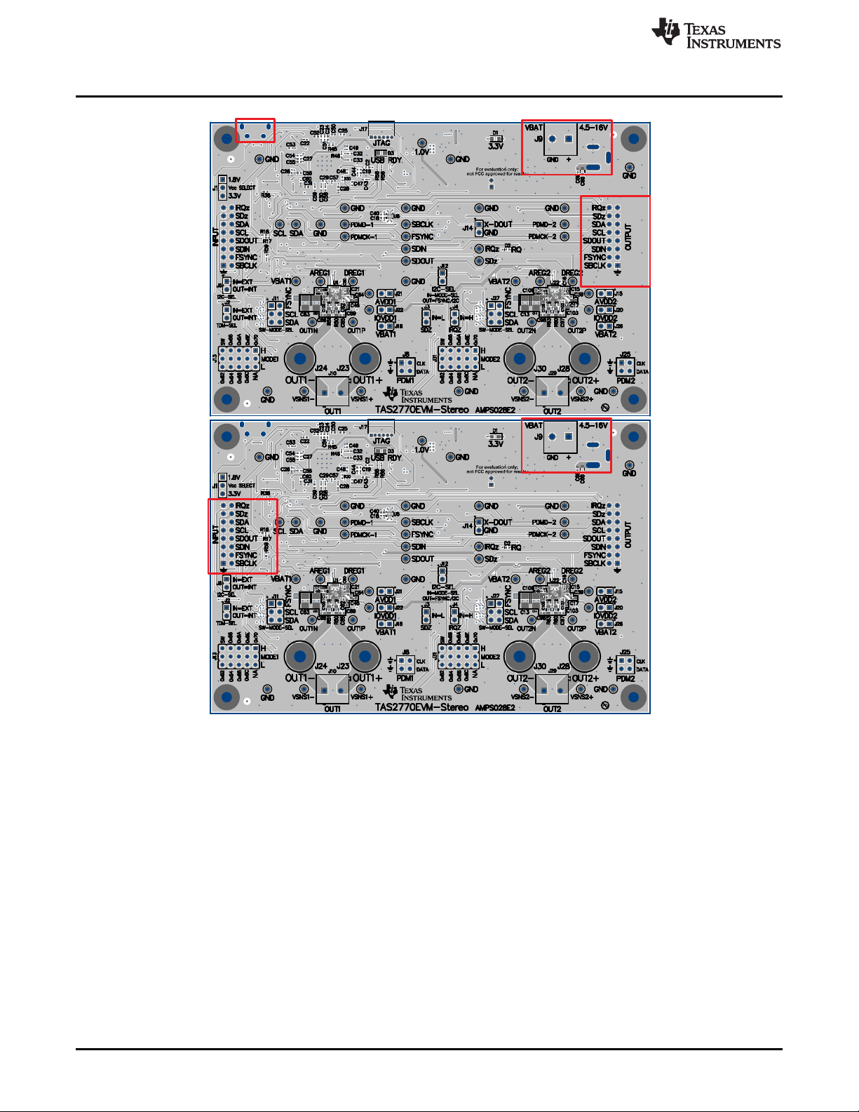
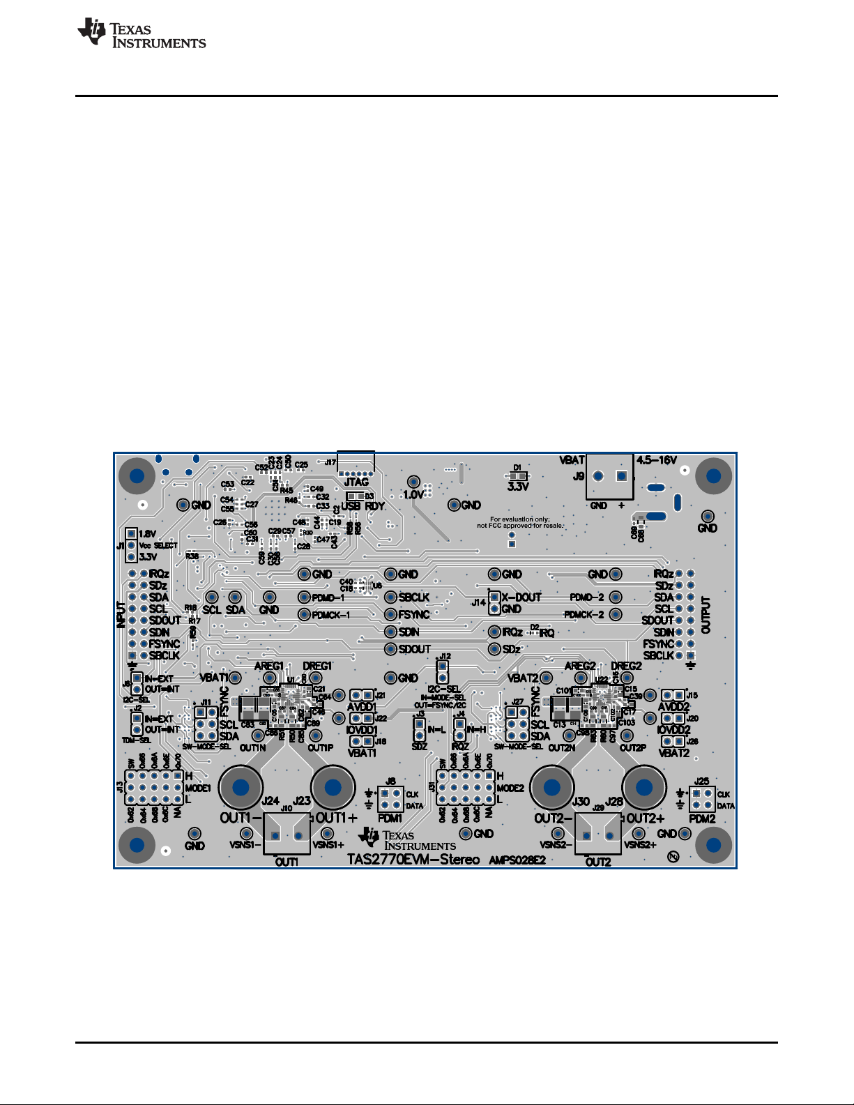
4 Stereo Setup
1. Install PurePath™ Console 3 with the TAS2770EVM-STEREO plug-in
2. Connect the first speaker to J10 on the EVM. Alternatively, J23 and J24 can be used for speaker
connections.
3. Connect a second speaker to J29 on the EVM. Alternatively, J28 and J30 can be used for speaker
connections.
4. Attach a power supply to connector J9. There is also an alternate barrel jack connector (J19) adjacent
to this connector.
5. Set jumper J13 to select the desired I2C address for channel 1.
6. Set jumper J31 to select the desired I2C address for channel 2.
2
TAS2770 Stereo Evaluation Module
Copyright © 2017, Texas Instruments Incorporated
SLOU497–October 2017
Submit Documentation Feedback
Page 3
www.ti.com
7. Connect the EVM to a Windows® 7+ PC with a micro-USB cable (J16).
Stereo Setup
Figure 1. TAS2770EVM-STEREO Stereo Configuration
8. Verify that the EVM is the default playback device by opening the sound dialog from the Windows®
Control Panel as shown in Figure 2.
Figure 2. Playback Device Settings
9. Set the sampling rate using the Windows® setting by opening Properties > Advanced. The
TAS2770EVM-STEREO supports 44.1 KHz and 48KHz sampling rates.
SLOU497–October 2017
Submit Documentation Feedback
Copyright © 2017, Texas Instruments Incorporated
TAS2770 Stereo Evaluation Module
3
Page 4
Mono Setup
10. Set the bit depth as desired using the Thesycon Control Panel accessible from the system tray shown
11. Proceed to configure the device using PPC3.
www.ti.com
in Figure 3.
Figure 3. Thesycon Driver Control Panel
Please refer to Figure 8 for default jumper settings.
5 Mono Setup
1. Install PurePath™ Console 3 with the TAS2770EVM-STEREO plug-in
2. Connect the first speaker to J10 on the EVM. Alternatively, J23 and J24 can be used for speaker
connections.
3. Attach a power supply to connector J9. There is also an alternate barrel jack connector (J19) adjacent
to this connector.
4. Set jumper J13 to select the desired I2C address for channel 1.
5. Connect the EVM to a Windows® 7+ PC with a micro-USB cable (J16).
4
TAS2770 Stereo Evaluation Module
Copyright © 2017, Texas Instruments Incorporated
SLOU497–October 2017
Submit Documentation Feedback
Page 5
www.ti.com
Multi-Channel Setup
Figure 4. TAS2770EVM-STEREO Mono Configuration
6. Verify that the EVM is the default playback device by opening the sound dialog from the Windows®
Control Panel as shown in Figure 2.
7. Set the sampling rate using the Windows® setting by opening Properties > Advanced. The
TAS2770EVM-STEREO supports 44.1 KHz and 48KHz sampling rates.
8. Set the bit depth as desired using the Thesycon Control Panel accessible from the system tray shown
in Figure 3.
9. Proceed to configure the device using PPC3.
6 Multi-Channel Setup
1. Install PurePath™ Console 3 with the TAS2770EVM-STEREO plug-in
2. Connect up to 4 TAS2770EVM-STEREOs together using connectors J5 and J7.
3. Attach a power supply to each board.
4. The leftmost board should have jumpers set to match the Stereo configuration. On all other boards
insert a jumper on J2 and J6. See Figure 5 for details.
5. Set Jumpers J13 and J31 on each board to a unique address.
6. Configure the sampling rate and bit depth as discussed in Mono Setup steps 6-8.
7. Proceed to configure the device using PPC3.
8. Connect the leftmost EVM to a Windows® 7+ PC with a micro-USB cable (J16).
SLOU497–October 2017
Submit Documentation Feedback
Copyright © 2017, Texas Instruments Incorporated
TAS2770 Stereo Evaluation Module
5
Page 6
Digital Audio Interfaces
www.ti.com
7 Digital Audio Interfaces
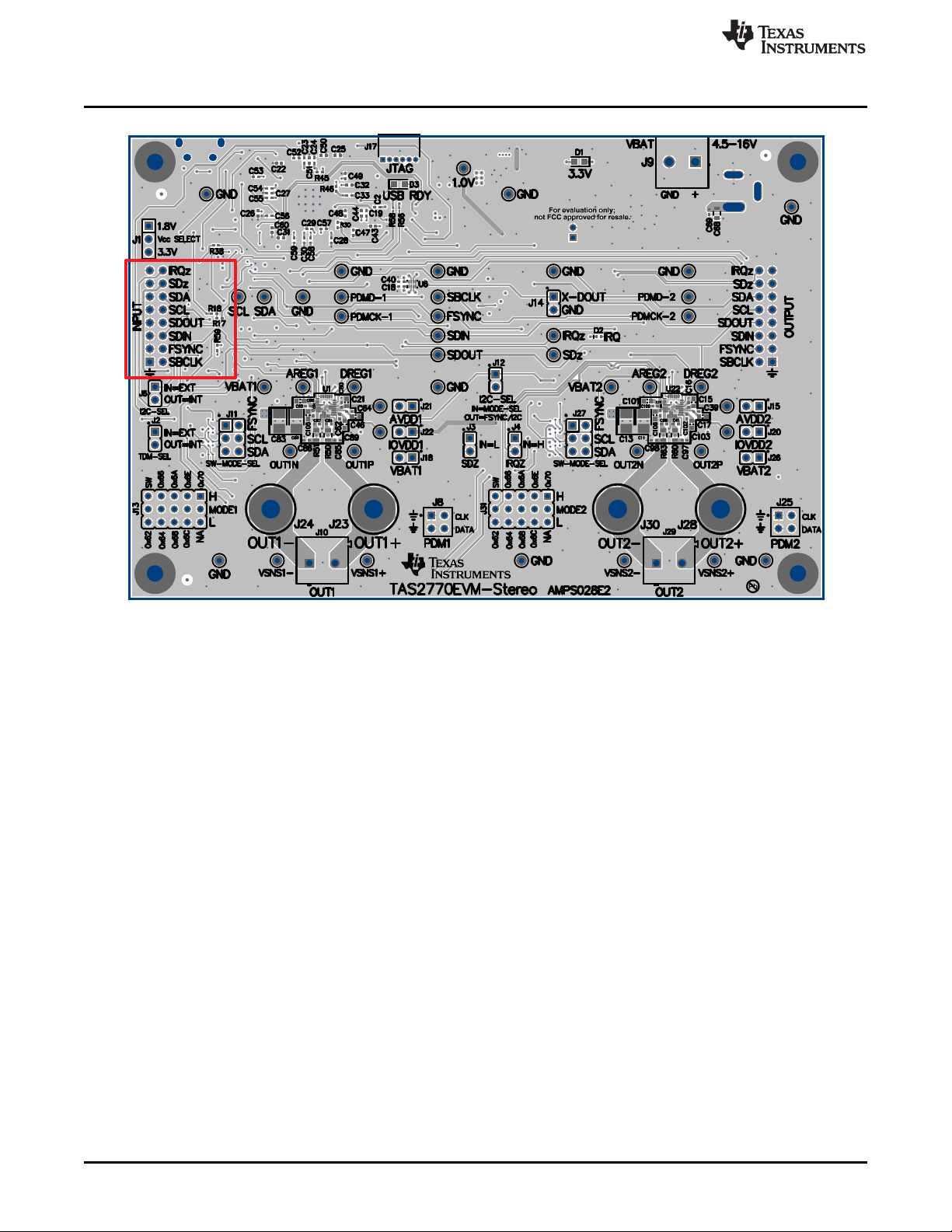
The various digital audio interfaces on the TAS2770 Reference Board can be selected through hardware
settings and software settings. Several headers close to the TAS2770 device allow access to the following
digital audio signals:
• I2S Data out(SDOUT) from the TAS2770 (for example, current and voltage sense data)
• I2S Data in(SDIN) to the TAS2770
• I2S Word clock or fram sync(FSYNC)
• I2S Bit clock(SBCLK)
• PDM Clock (PDMCLK0) – optional input source for TAS2770
• PDM Clock (PDMCLK1) – optional input source for TAS2770
• PDM Data (PDMD0) – optional input source for TAS2770
• PDM Data (PDMD1) – optional input source for TAS2770
• I2C Clock (SCLK)
6
TAS2770 Stereo Evaluation Module
Figure 5. Multi-Channel Setup
Copyright © 2017, Texas Instruments Incorporated
SLOU497–October 2017
Submit Documentation Feedback
Page 7
www.ti.com
• I2C Data (SDA)
TAS2770 can be configured for SoundwireSM Mode as well:
• SoundwireSM clock - SBCLK
• SoundwireSM data - SDOUT
• SoundwireSM address – SDA
• SoundwireSM address – FSYNC
• SoundwireSM address – SCL
A jumper inserted in the SW slot of J13 sets the TAS2770 to SoundwireSM mode. Then J11 can be
set as desired to configure the device address.
The selection between USB (internal) and External inputs is controlled by jumpers J2 and J6.
These jumpers set TDM and I2C respectively.
7.1 Digital Audio Interface Selection
7.1.1 USB
The TAS2770 Reference Board contains an XMOS microcontroller that acts as a USB HID and USBclass audio interface. To select USB, remove jumpers J6 and J2. Insert a jumper in J12. This is shown
in Figure 6.
Digital Audio Interfaces
7.1.2 Direct (AP/PSIA)
Insert a jumper on J2 and connect the external digital audio source (for example AP or PSIA) to the
external input header pin. The odd numbered pins on this header provide a ground for each signal.
This is shown in Figure 9. Note that the jumper setting for J1 must reflect the logic level of the external
source.
SLOU497–October 2017
Submit Documentation Feedback
Figure 6. USB Audio Input Configuration
Copyright © 2017, Texas Instruments Incorporated
TAS2770 Stereo Evaluation Module
7
Page 8
Digital Audio Interfaces
www.ti.com
Figure 7. AP/PSIA Input Configuration
8
TAS2770 Stereo Evaluation Module
Copyright © 2017, Texas Instruments Incorporated
SLOU497–October 2017
Submit Documentation Feedback
Page 9
GND
1.0V
0.1µF
16V
C56
GND
1.0V
0.1µF
16V
C55
GND
1.0V
0.1µF
16V
C47
GND
1.0V
0.1µF
16V
C48
GND
1.0V
0.1µF
16V
C49
GND
1.0V
0.1µF
16V
C50
GND
1.0V
0.1µF
16V
C51
GND
1.0V
0.1µF
16V
C52
GND
1.0V
0.1µF
16V
C53
GND
1.0V
0.1µF
16V
C54
GND
1.0V
0.1µF
16V
C57
GND
1.0V
0.1µF
16V
C58
GND
1.0V
0.1µF
16V
C59
GND
1.0V
0.1µF
16V
C60
3.3V 1.0V
3.3V
1.0V
GND
4.7
R23
0.1µF
C42
GND
X-SDZ_CTRL
X-SDZ
IRQZ-3.3V
X-QSPI-CS
1.0k
R16
2.2k
R17
2.2k
R18
3.3V 3.3V 3.3V
GND
0.1µF
16V
C32
3.3V
GND
0.1µF
16V
C40
3.3V
GND
0.1µF
16V
C35
3.3V
GND
0.1µF
16V
C19
1.8V
X-SDA
X-SCL
GND
0.1µF
16V
C34
3.3V
GND
0.1µF
16V
C18
1.8V
GND
0.1µF
16V
C33
3.3V
GND
0.1µF
16V
C20
1.8V
GND
0.1µF
16V
C28
3.3V
GND
0.1µF
16V
C22
3.3V
GND
0.1µF
16V
C29
3.3V
GND
0.1µF
16V
C30
3.3V
GND
0.1µF
16V
C26
3.3V
GND
0.1µF
16V
C27
3.3V
GND
0.1µF
16V
C25
3.3V
GND
0.1µF
16V
C24
3.3V
GND
0.1µF
16V
C23
3.3V
GND
0.1µF
16V
C31
3.3V
GND
0.1µF
16V
C43
3.3V
GND
0.1µF
16V
C44
3.3V
GND
0.1µF
16V
C45
3.3V
X-DOUT
X-BCLK
X-LRCK
X-SDA
X-SCL
X-SDZ
X-SDZ_CTRL
I2C
I2S
SHUTDOWN
X-DIN
TO
MUXES
AND
TRANSLATORS
VDDIOL
6
VDD
11
VDDIOL
14
VDD
16
VDD
17
VDDIOL
19
VDD
24
VDDIOL
29
VDD
36
VDD
41
VDDIOL
42
VDDIOR
52
VDD
56
VDD
60
NC
65
VDDIOR
67
VDD
73
VDDIOR
78
VDD
80
VDD
81
VDDIOR
83
VDD
87
VDDIOR
92
VDD
101
VDD
102
PLL_AVDD
103
PLL_AGND
104
OTP_VCC
105
VDDIOT
110
VDDIOT
111
VDD
120
USB_VDD33
44
USB_VDD
49
NC
50
VDD
126
PAD
129
U5E
XEF216-512-TQ128-C20
X1D35
13
X1D36
15
X1D37
18
X1D38
20
X1D18
25
X1D19
26
X1D14
51
X1D15
53
X1D20
54
X1D21
55
X1D02
72
X1D03
74
X1D04
75
X1D05
76
X1D06
77
X1D07
79
X1D08
82
X1D09
84
X1D00
85
X1D01
86
X1D41
107
X1D42
108
X1D43
109
X1D40
106
X1D26
112
X1D27
113
X1D28
114
X1D29
115
X1D30
116
X1D31
117
X1D32
118
X1D33
119
X1D39
21
X1D16
22
X1D17
23
X1D10
121
X1D11
122
U5B
XEF216-512-TQ128-C20
GND
USB-DP
USB-DM
USB-ID
VBUS-IN
L2
43.2
R29
GND
100k
R28
0.1µF
C61
GND GND
USB_ID
43
USB_VBUS
45
USB_DP
46
USB_DM
47
USB_RTUNE
48
U5C
XEF216-512-TQ128-C20
VBUS
1
D-
2
D+
3
ID
4
GND
5
678
9
J16
USB
X0D36
3
X0D37
4
X0D38
5
X0D39
7
X0D40
8
X0D41
9
X0D42
10
X0D43
12
X0D01
27
X0D10
28
X0D00
30
X0D04
31
X0D11
32
X0D05
33
X0D06
34
X0D07
35
X0D02
37
X0D03
38
X0D08
39
X0D09
40
X0D14
57
X0D15
58
X0D20
59
X0D21
61
X0D12
62
X0D13
63
X0D22
64
X0D23
66
X0D16
68
X0D17
69
X0D18
70
X0D19
71
X0D24
88
X0D25
89
X0D34
90
X0D35
91
X0D26
93
X0D27
94
X0D32
95
X0D28
96
X0D33
97
X0D29
98
X0D30
99
X0D31
100
U5A
XEF216-512-TQ128-C20
X-SPI-SS0
X-SPI-SS1
X-SPI-SS2
X-SPI-SS3
47k
R19
3.3V
47k
R20
3.3V
47k
R21
3.3V
47k
R22
3.3V
10k
R5
3.3V
10k
R46
3.3V
10k
R45
3.3V
IRQ
IRQZ-3.3V
IRQZ-3.3V
3.3V
Blue
D3
USB RDY
680
R6
10.0k
R9
GND-USB
2.2µF
C3
GND
X-TCK
X-TMS
X-TDO
X-TDI
X-TRSTN
VDD
4
OE/STANDBY1GND
2
OUT
3
24
MHz
Y1
3.3V
3.3V
1A
1
GND
2
2A32Y
4
VCC
5
1Y
6
U9
SN74LVC2G07DSFR
0
R30
TRST
123
RST
124
CLK
125
TMS
127
TCK
128
TDO
1
TDI
2
XEF216-512-TQ128-C20
U5D
X-RSTN
X-TCK
X-TMS
X-TDO
X-TDI
3.3V
GND
3.3V
GND
X-24M
XIN/CLK
1
S0
2
VDD
3
VCTRL
4
GND
5
VDDOUT
6
VDDOUT
7
Y3
8
Y2
9
GND
10
Y1
11
SCL/S2
12
SDA/S1
13
XOUT
14
U14
CDCE913PWR
GND
1.8V 3.3V
X-SDA
X-SCL
GND
VCCA
1
A1
2
A2
3
GND
5
B2
6
B1
7
OE
4
VCCB
8
U8
SN74AVC2T244DQMR
GND GND
3.3V 1.8V
ENABLE
1
GND
2
SENSE
3
SENSE_OUT
4
CT
5
VCC
6
U7
TPS3897ADRYR
3.3V
25.5k
R24
1.0V
51.0k
R31
10.0k
R25
3.3V
470pF
C4
GND
GND
GND
10.0k
R26
10.0k
R27
10.0k
R8
33.2
R57 X-24M
GND
0.1µF
16V
C1
GND
0.1µF
16V
C2
1.8V 1.8V
X-MCLK
X-BCLK
X-MCLK
X-MCLK
33.2R56
33.2R58
33.2R7
33.2R32
33.2R33
33.2R55
33.2R54
X-TCK
X-TMS
X-TDO
X-TDI
X-TRSTN
1
2
3
4
5
6
J17
JTAG
GND
GND
0.1µF
16V
C104
3.3V
www.ti.com
8 Hardware Documentation
8.1 TAS2770EVM-STEREO Schematics
Hardware Documentation
SLOU497–October 2017
Submit Documentation Feedback
Figure 8. Schematic: XMOS USB Controller
Copyright © 2017, Texas Instruments Incorporated
TAS2770 Stereo Evaluation Module
9
Page 10
FSYNC
SCL
SDA
SDZ
I2S
SDZ
33.2
R2
>
X-SCL
X-SCL
X-SDA
X-BCLK
XMOS
X-BCLK
X-LRCK
X-DOUT
FSYNC
S
1
1B1
2
1B2
3
1A
4
2B1
5
2B2
6
GND
8
3A
9
3B2
10
3B1
11
4A
12
4B2
13
4B1
14
2A
7
OE
15
VCC
16
U17
SN74CB3Q3257DGVR
3.3V
GND
GND
I2C/SHUTDOWN SOURCE SELECT
10.0k
R44
OUT=INTERNAL
IN=EXTERNAL
S
1
1B1
2
1B2
3
1A
4
2B1
5
2B2
6
GND
8
3A
9
3B2
10
3B1
11
4A
12
4B2
13
4B1
14
2A
7
OE
15
VCC
16
U12
SN74CB3Q3257DGVR
3.3V
GND
GND
TDM SOURCE SELECT
>
>
10.0k
R41
GND
OUT=INTERNAL
IN=EXTERNAL
33.2R38
33.2
R39
33.2
R40
J6
I2C-SEL
3.3V
J2
TDM-SEL
3.3V
GND
X-SDZ
>
>
>
>
>
>
3.3V-1.8V TRANSLATORS (Lev el Shifters)
FSYNC-XLTR
GND
Vcc
SDOUT-XLTR
DIR1
15
DIR2
16
A1
1
A2
2
A3
3
A4
4
DIR3
5
DIR4
6
OE
7
GND
8
B4
9
B3
10
B2
11
B1
12
VCCB
13
VCCA
14
U11
SN74AVC4T774RSVR
1.8V
GND
SBCLK-XLTR
>
>
>
>
>
>
>
>
SDZ-XTLR
1
2
3
4
5
U18
LVC1G125
1.8V
GND
XMOS
EXT-IN
SBCLK-EXTIN
SCL-EXTIN
SDA-EXTIN
SBCLK-EXTIN
FSYNC-EXTIN
SDIN-EXTIN
FSYNC-EXTIN
SDIN-EXTIN
X-SDZ
>
X-SDA
SCL-EXTIN
EXT-IN
SDA-EXTIN
I2C
I2S
X-LRCK
>
X-DOUT
>
SHUTDOWN
XMOS
EXT-IN
SDZ-EXTIN
SDZ-EXTIN
>
SDZ-XTLR
SCL-XLTR
SDA-XLTR
I2C
SHUTDOWN
>
>
> >
TO DUT
EXT-OUT
AND
TO DUT AND
EXT-OUT
TO DUT AND EXT-OUT
>
>
>
1.8V
SCL
SDA
3.3V
GND
SDA_B
1
GND
2
VCCA
3
SDA_A
4
SCL_A
5
OE
6
VCCB
7
SCL_B
8
U15
TCA9406DCUR
10k
R43
SCL-XLTR
SDA-XLTR
X-SDZ_CTRL
>
0.1µF
16V
C5
GND
Vcc
SBCLK
33.2
R1 SBCLK
SDIN
33.2
R3 SDIN
GND
0.1µF
16V
C36
GND
0.1µF
16V
C37
1.8V 1.8V
SDZ-CTRL
>
SDZ-CTRL
X-SDZ_CTRL
>
10.0k
R59
3.3V
Hardware Documentation
www.ti.com
10
TAS2770 Stereo Evaluation Module
Figure 9. Schematic: Input Multiplexing and Level Shift
Copyright © 2017, Texas Instruments Incorporated
SLOU497–October 2017
Submit Documentation Feedback
Page 11
GND
SBCLK-EXTIN
FSYNC-EXTIN
SDIN-EXTIN
SDOUT
SCL-EXTIN
SDA-EXTIN
SDZ-EXTIN
IRQZ
INPUT HEADER
0.1µF
16V
C8
GND
3.3V
0.1µF
16V
C9
GND
3.3V
0.1µF
16V
C10
GND
3.3V
(EXT)
GND
2
1
4
5
3
U16
SN74LV1T126DCKR
GND
Blue
D2
IRQ
360
R42
3.3V
IRQZ LED
SDIN-EXTOUT
SDOUT
SBCLK-EXTOUT
FSYNC-EXTOUT
SDA-EXTOUT
SDZ
IRQZ
>
<
SDZ
IRQZ
SCL-EXTOUT
<
>
0.1µF
16V
C11
GND
3.3V
1.8V
47kR34
GND
2.2kR36
1.8V
IRQZ Pullup
SDZ Control
J3
SDZ
10.0kR37
IRQZ
SDZ
>
>
>
<
CONTROL
SDZ-EXTIN
SCL-EXTIN
I2C
SDA-EXTIN
I2S
SBCLK-EXTIN
FSYNC-EXTIN
SDIN-EXTIN
OUTPUT HEADER
<
>
>
>
SCL
I2C
SDA
SBCLK
FSYNC
SDOUT
I2S
TO MUXES
FROM DUT OR
GND
DIR1
15
DIR2
16
A1
1
A2
2
A3
3
A4
4
DIR3
5
DIR4
6
OE
7
GND
8
B4
9
B3
10
B2
11
B1
12
VCCB
13
VCCA
14
U3
SN74AVC4T774RSVR
1.8V
GND
SCL
SDA
3.3V
GND
SDA_B
1
GND
2
VCCA
3
SDA_A
4
SCL_A
5
OE
6
VCCB
7
SCL_B
8
U4
TCA9406DCUR
10k
R4
SDA-EXTOUT
SCL-EXTOUT
SDIN-EXTOUT
SBCLK-EXTOUT
FSYNC-EXTOUT
>
>
>
>
SDIN
SDZ
CONTROL
>
>
>
>
IRQZ
LEVEL SHIFTERS
>
VCCA
1
A1
2
A2
3
GND
5
B2
6
B1
7
OE
4
VCCB
8
U6
SN74AVC2T244DQMR
GND
1.8V3.3V
X-DIN
IRQZ-3.3V
SDOUT
IRQZ
TO XMOS
>
GND
123
J1
Vcc SELECT
Vcc 1.8V3.3V
Vcc
1.8V
3.3V
0.1µF
16V
C6
GND
Vcc
GND
0.1µF
16V
C38
1.8V
J14
X-DOUT
X-DIN
GND
J4
IRQZ
1 2
3 4
5 6
7 8
9 10
11 12
13 14
15 16
J7
INPUT
1
3
56
4
2
7
910
8
12 11
14 13
16 15
J5
OUTPUT
www.ti.com
Hardware Documentation
SLOU497–October 2017
Submit Documentation Feedback
Figure 10. Schematic: External Input / Output Routing
Copyright © 2017, Texas Instruments Incorporated
TAS2770 Stereo Evaluation Module
11
Page 12

GND
GND GND
1.8V
SBCLK
FSYNC
SDIN
SDOUT
GND
SCL
SDZ
IRQZ
GND
GND
100pF
C85
DNP
DNP
0
R50
GND GND
PDM#1 Header
Soundwire Mode Settings #1
Mode Settings
To
0.1µF
25V
C81
GND
PDMCK0-1
PDMD0-1
PDMD1-1
PDMCK1-1
GND
TP9
VSNS1+
TP10
VSNS1-
1.8V
GND
12
34
56
J11
SW-MODE-SEL
0.1µF
25V
C80
1µF
10V
C79
0.1µF25V
C84
0.1µF25V
C87
1µF
10V
C88
1µF
10V
C89
47k
R14
10.0k
R11
2.2k
R13
470
R12
OUTPUT #1
0
R51
SDIN
SDOUT
SBCLK
FSYNC1
SCL1
SDA1
SDZ
IRQZ
MODE1
100pF
C86
DNP
DNP
22µF
20V
C82
22µF
20V
C83
GND
OUT1+
OUT1-
GND
FSYNC1
SCL1
SDA1
10.0k
R15
10.0k
R53
10.0k
R52
GND
1.8V
0.1µF
16V
C78
GND
3.3V
1 2
3 4
5 6
7 8
J8
PDM1
0.1µF
25V
C63
GND
0.1µF
25V
C62
GND
TP18
DREG1
TP19
AREG1
TP15
AVDD1
TP14
VBAT1
TP16
OUT1P
TP17
OUT1N
TP20
GND
GND
TP21
GND
GND
TP22
GND
GND
TP23
GND
GND
OUTP1
OUTN1
TP24
IOVDD1
GND
0.1µF
25V
C64
J23
OUT1+
J24
OUT1-
AVDD1
IOVDD1
DREG1
AREG1
TDM/Control
Bus
GND
2.2µF
10V
C21
GND
1µF
10V
C46
TP25
PDMD1-1
TP7
SDZ
TP8
IRQZ
TP5
SCL
TP2
FSYNC
1
2
3
4
567
8
9
10
111213
14
15
J13
MODE1
MODE1
TP12
GND
GND
TP13
GND
GND
BSTP1
BSTN1
I2C-SEL_CTRL
1A
A1
1B
B1
1C
B2
GND
D1
2A
D2
2B
C2
2C
C1
VCC
A2
U2
SN74LVC2G66YZPR
0.1µF
16V
C94
GND
3.3V
3.3V
GND
1A
A1
1B
B1
1C
B2
GND
D1
2A
D2
2B
C2
2C
C1
VCC
A2
U20
SN74LVC2G66YZPR
3.3V
GND
1A
A1
1B
B1
1C
B2
GND
D1
2A
D2
2B
C2
2C
C1
VCC
A2
U21
SN74LVC2G66YZPR
3.3V
SDA
TP6
SDA
3.3V
10.0k
R35
GND
J12
I2C-SEL
0.1µF
16V
C95
GND
3.3V
2 4
5
3
U27
LVC1G14
GND
FSYNC
SCL
SDA
I2C-SEL_CTRL
I2C-SEL_CTRL
I2C-SEL_CTRL
0.1µF
16V
C96
GND
3.3V
To
TDM/Control
Bus
3.3V
TP26
PDMCK0-1
TP27
PDMD0-1
TP28
PDMCK1-1
VBAT
VBAT1
PDMCK0-1
PDMD0-1
PDMD1-1
PDMCK1-1
TP47
SBCLK
TP46
SDOUT
TP45
SDIN
I2C-SEL_CTRL
TO TAS2772 #2
J10
OUT1
J18
VBAT1
J21
AVDD1
J22
IOVDD1
OUT1+
OUT1-
1µF
25V
C105
GND
SBCLK
13
SCL
23
SDA
22
SD
21
MODE
19
BST_P
4
VBAT
25
AVDD
9
IOVDD
8
DREG
7
OUT_P
3
OUT_N
26
VSNS_P
5
PGND
2
FSYNC
14
SDIN
11
SDOUT
12
PDMCK0
15
PDMD0
16
PDMCK1
17
PDMD1
18
IRQ
20
VSNS_N
6
BST_N
1
AREG
24
GND
10
U1
TAS2770RJQ
Hardware Documentation
www.ti.com
12
TAS2770 Stereo Evaluation Module
Figure 11. Schematic: TAS2770 Channel 1 Control
Submit Documentation Feedback
SLOU497–October 2017
Copyright © 2017, Texas Instruments Incorporated
Page 13

GND GND
1.8V
SBCLK
FSYNC
SDIN
SDOUT
SCL
SDZ
IRQZ
GND
GND
100pF
C97
0 R60
GND GND
Soundwire Mode Settings #2
Mode Settings
To
0.1µF
25V
C12
GND GND
1.8V
GND
12
34
56
J27
SW-MODE-SEL
0.1µF
25V
C16
1µF
10V
C7
0.1µF25V
C41
0.1µF25V
C99
1µF
10V
C101
1µF
10V
C103
47k
R68
10.0k
R65
2.2k
R67
470
R66
0 R63SDIN
SDOUT
SBCLK
FSYNC2
SCL2
SDA2
SDZ
IRQZ
PDMD-2
PDMCK-2
MODE2
100pF
C98
22µF
20V
C13
22µF
20V
C14
GND
GND
FSYNC2
SCL2
SDA2
10.0k
R61
10.0k
R62
10.0k
R64
GND
1.8V
0.1µF
16V
C90
GND
3.3V
0.1µF
25V
C100
GND
0.1µF
25V
C102
GND
TP3
DREG2
TP4
AREG2
TP37
AVDD2
TP31
VBAT2
TP38
OUT2P
TP1
OUT2N
TP33
GND
GND
TP34
GND
GND
TP35
GND
GND
TP36
GND
GND
TP32
IOVDD2
GND
0.1µF
25V
C39
AVDD2
IOVDD2
TDM/Control
Bus
GND
2.2µF
10V
C15
GND
1µF
10V
C17
TP42
PDMD-2
1
2
3
4
567
8
9
10
111213
14
15
J31
MODE2
MODE2
TP29
GND
GND
TP30
GND
GND
I2C-SEL_CTRL
1A
A1
1B
B1
1C
B2
GND
D1
2A
D2
2B
C2
2C
C1
VCC
A2
U23
SN74LVC2G66YZPR
0.1µF
16V
C91
GND
3.3V
3.3V
GND
1A
A1
1B
B1
1C
B2
GND
D1
2A
D2
2B
C2
2C
C1
VCC
A2
U24
SN74LVC2G66YZPR
3.3V
GND
1A
A1
1B
B1
1C
B2
GND
D1
2A
D2
2B
C2
2C
C1
VCC
A2
U25
SN74LVC2G66YZPR
3.3V
SDA
0.1µF
16V
C92
GND
3.3V
2 4
5
3
U26
LVC1G14
GND
FSYNC
SCL
SDA
I2C-SEL_CTRL
I2C-SEL_CTRL
I2C-SEL_CTRL
0.1µF
16V
C93
GND
3.3V
To
TDM/Control
Bus
3.3V
TP41
PDMCK-2
VBAT
VBAT2
OUT2+
OUT2-
OUTP2
OUTN2
DREG2
AREG2
BSTP2
BSTN2
I2C-SEL_CTRL
J26
VBAT2
J20
IOVDD2
J15
AVDD2
1µF
25V
C106
GND
SBCLK
13
SCL
23
SDA
22
SD
21
MODE
19
BST_P
4
VBAT
25
AVDD
9
IOVDD
8
DREG
7
OUT_P
3
OUT_N
26
VSNS_P
5
PGND
2
FSYNC
14
SDIN
11
SDOUT
12
GND
15
GND
16
PDMCK
17
PDMD
18
IRQ
20
VSNS_N
6
BST_N
1
AREG
24
GND
10
U22
TAS2770RJQ
GND
PDM#2 Header
PDMD-2
PDMCK-2
1 2
3 4
J25
PDM2
TP43
VSNS2+
TP44
VSNS2-
OUT2-
OUT2+
OUTPUT #2
J28
OUT2+
J30
OUT2-
J29
OUT2
GND
www.ti.com
Hardware Documentation
SLOU497–October 2017
Submit Documentation Feedback
Figure 12. TAS2770 Channel 2 Control
TAS2770 Stereo Evaluation Module
13
Copyright © 2017, Texas Instruments Incorporated
Page 14

360
R47
GND
Green
D13.3V
3.3V
10µF
C66
GND
0.1µF
50V
C70
GND GND GND
3.3V
GND
IN1OUT
3
4
U19
TL760M33QKVURQ1
GND
L1
0.1µF
16V
C65
47µF
16V
C71
VBAT
EN
1
PG
2
FB
3
VOS
4
GND
5
SW
6
VIN
7
U10
TPS62085RLTR
22µF
C73
470nH
L3
40.2k
R48
162k
R10
1.00M
R49
5V to 1V BUCK LDO
TP11
1.0V
0.1µF
C74
22µF
C72
1.0V
GND
GND
GND
GND GND
3.3V
IN
1
2
EN3NR
4
OUT
5
GND
U13
TPS73618DBVR
0.1µF
C76
0.01µF
C77
1.8V
GND
GND
GND
GND
3.3V
1µF
10V
C75
5V-VR
VBAT
GND
1µF
50V
C68
VBAT RANGE = 4.5-16V
47µF
63V
C67
0.1µF
25V
C69
1
3
2
J19
VBAT
1
2
J9
Hardware Documentation
www.ti.com
14
TAS2770 Stereo Evaluation Module
Figure 13. On-Board Power
Copyright © 2017, Texas Instruments Incorporated
SLOU497–October 2017
Submit Documentation Feedback
Page 15

www.ti.com
8.2 TAS2770 Reference Board Printed Circuit Board Layout
Hardware Documentation
SLOU497–October 2017
Submit Documentation Feedback
Figure 14. PCB: Top Silkscreen
Copyright © 2017, Texas Instruments Incorporated
TAS2770 Stereo Evaluation Module
15
Page 16

Hardware Documentation
www.ti.com
16
TAS2770 Stereo Evaluation Module
Figure 15. PCB: Top Solder Mask
SLOU497–October 2017
Submit Documentation Feedback
Copyright © 2017, Texas Instruments Incorporated
Page 17

www.ti.com
Hardware Documentation
SLOU497–October 2017
Submit Documentation Feedback
Figure 16. PCB: Top Copper
Copyright © 2017, Texas Instruments Incorporated
TAS2770 Stereo Evaluation Module
17
Page 18

Hardware Documentation
www.ti.com
18
TAS2770 Stereo Evaluation Module
Figure 17. PCB: Copper Layer 2
SLOU497–October 2017
Submit Documentation Feedback
Copyright © 2017, Texas Instruments Incorporated
Page 19

www.ti.com
Hardware Documentation
SLOU497–October 2017
Submit Documentation Feedback
Figure 18. PCB: Copper Layer 3
Copyright © 2017, Texas Instruments Incorporated
TAS2770 Stereo Evaluation Module
19
Page 20

Hardware Documentation
www.ti.com
20
TAS2770 Stereo Evaluation Module
Figure 19. PCB: Bottom Copper
SLOU497–October 2017
Submit Documentation Feedback
Copyright © 2017, Texas Instruments Incorporated
Page 21

www.ti.com
Hardware Documentation
SLOU497–October 2017
Submit Documentation Feedback
Figure 20. PCB: Bottom Solder Mask
Copyright © 2017, Texas Instruments Incorporated
TAS2770 Stereo Evaluation Module
21
Page 22

Hardware Documentation
www.ti.com
22
TAS2770 Stereo Evaluation Module
Figure 21. PCB: Bottom Silk Screen
SLOU497–October 2017
Submit Documentation Feedback
Copyright © 2017, Texas Instruments Incorporated
Page 23

www.ti.com
8.3 TAS2770 Reference Board Bill of Materials
Table 2. TAS2770 Reference Board Bill of Materials
Hardware Documentation
Designator Qty Value Description Package Reference Part Number Manufacturer Alternate Part
!PCB1 1 Printed Circuit
C1, C2, C5, C6,
C8, C9, C10,
C11, C18, C19,
C20, C22, C23,
C24, C25, C26,
C27, C28, C29,
C30, C31, C32,
C33, C34, C35,
C36, C37, C38,
C40, C43, C44,
C45, C47, C48,
C49, C50, C51,
C52, C53, C54,
C55, C56, C57,
C58, C59, C60,
C78, C90, C91,
C92, C93, C94,
C95, C96, C104
C3 1 2.2 µF CAP, CERM, 2.2
C4 1 470 pF CAP, CERM,
C7, C17, C46,
C75, C79, C88,
C89, C101, C103
C12, C16, C39,
C41, C62, C63,
C64, C69, C80,
C81, C84, C87,
C99, C100, C102
C13, C14, C82,
C83
55 0.1 µF CAP, CERM, 0.1
9 1 µF CAP, CERM, 1
15 0.1 µF CAP, CERM, 0.1
4 22 µF CAP, Tantalum
Board
µF, 16 V, ±10%,
X7R, 0402
µF, 10 V, ± 10%,
X7R, 0603
470 pF, 25 V, ±
5%, C0G/NP0,
0402
µF, 10 V, ± 10%,
X7R, 0603
µF, 25 V, ± 20%,
X7R, 0402
Polymer, 22 µF,
20 V, ± 20%,
0.09 Ω, 3528-21
SMD
0402 GRM155R71C10
0603 GRM188R71A22
0402 GRM1555C1E47
0603 GRM188R71A10
0402 C1005X7R1E104
3528-21 TCJB226M020R
NA Any - -
MuRata
4KA88D
MuRata
5KE15D
MuRata
1JA01D
MuRata
5KA61D
TDK
M050BB
AVX
0090
Number
Alternate
Manufacturer
SLOU497–October 2017
Submit Documentation Feedback
Copyright © 2017, Texas Instruments Incorporated
TAS2770 Stereo Evaluation Module
23
Page 24

Hardware Documentation
Table 2. TAS2770 Reference Board Bill of Materials (continued)
C15, C21 2 2.2 µF CAP, CERM, 2.2
C42, C61, C65,
C74
C66 1 10 µF CAP, CERM, 10
C67 1 47 µF CAP, AL, 47 µF,
C68 1 1 µF CAP, CERM, 1
C70 1 0.1 µF CAP, CERM, 0.1
C71 1 47 µF CAP, AL, 47 µF,
C72, C73 2 22 µF CAP, CERM, 22
C76 1 0.1 µF CAP, CERM, 0.1
C77 1 0.01 µF CAP, CERM,
C105, C106 2 1 µF CAP, CERM, 1
D1 1 Green LED, Green,
D2 1 Blue LED, Blue, SMD Blue LED SMLP12BC7TT86Rohm
4 0.1 µF CAP, CERM, 0.1
µF, 10 V,± 10%,
X7R, 0603
µF, 16 V, ± 10%,
X7R, 0402
µF, 35 V, ± 10%,
X7R, 1206
63 V, ± 20%,
0.65 Ω, AECQ200 Grade 2,
SMD
µF, 50 V, ± 10%,
X7R, 0805
µF, 50 V, ± 10%,
X7R, 0603
16 V, ± 20%, 0.8
Ω, AEC-Q200
Grade 2, TH
µF, 10 V, ± 20%,
X7R, 0805
µF, 10 V, ± 10%,
X7R, 0402
0.01 µF, 6.3 V, ±
10%, X7R, 0402
µF, 25 V,± 10%,
X5R, 0603
SMD
0603 C1608X7R1A225
K080AC
0402 GRM155R71C10
4KA88D
1206 GMK316AB7106KLTaiyo Yuden
SMT Radial F EEE-FK1J470P Panasonic
0805 GRM21BR71H10
5KA12L
0603 GCM188R71H10
4KA57D
D5xL11mm EEU-FC1C470 Panasonic
0805 GRM21BZ71A22
6ME15L
0402 GRM155R71A10
4KA01D
0402 GRM155R70J10
3KA01D
0603 GRM188R61E10
5KA12D
LED_0805 LTST-C171GKT Lite-On
TDK
MuRata
MuRata
MuRata
MuRata
MuRata
MuRata
MuRata
www.ti.com
D3 1 Blue LED, Blue, SMD LED_0805 LTST-C170TBKT Lite-On
24
TAS2770 Stereo Evaluation Module
Copyright © 2017, Texas Instruments Incorporated
SLOU497–October 2017
Submit Documentation Feedback
Page 25

www.ti.com
Table 2. TAS2770 Reference Board Bill of Materials (continued)
H1, H2, H3, H4 4 Machine Screw,
H5, H6, H7, H8 4 Standoff, Hex,
J1 1 Header, 100mil,
J2, J3, J4, J6,
J12, J14, J15,
J18, J20, J21,
J22, J26
J5 1 Receptacle,
J7 1 Header, 100mil,
J8, J25 2 Header, 100mil,
J9 1 Terminal Block,
J10, J29 2 Terminal Block, 5
J11, J27 2 Header, 100mil,
J13, J31 2 Header, 2.54mm,
J16 1 Connector,
J17 1 Receptacle,
J19 1 Power Jack,
12 Header, 100mil,
Round, #4-40 x
1/4, Nylon,
Philips panhead
0.5"L #4-40
Nylon
3x1, Gold, TH
2x1, Gold, TH
100mil, 8x2,
Gold, R/A, TH
8x2, Gold, R/A,
TH
4x2, Tin, TH
5.08mm, 2x1, TH
mm, 2x1, Tin, TH
3x2, Gold, TH
5x3, Gold, TH
Receptacle,
Micro-USB Type
AB, R/A, Bottom
Mount SMT
50mil, 6x1, Gold,
R/A, TH
mini, 2.5mm OD,
R/A, TH
Hardware Documentation
Screw NY PMS 440
Standoff 1902C Keystone - -
PBC03SAAN PBC03SAAN Sullins
Sullins 100 mil, 1 × 2, 230 mil above
insulator
SSQ-108-02-G-D-RA SSQ-108-02-G-
8x2 R/A Header TSW-108-08-G-
Header, 4x2, 100mil, Tin PEC04DAAN Sullins
Terminal Block, 5.08mm, 2x1, TH 0395443002 Molex
Terminal Block, 5 mm, 2x1, TH 691 101 710 002 Wurth Elektronik
Sullins 100mil, 2x3, 230 mil above
insulator
Header, 2.54mm, 5x3, TH 804-10-015-10-
Connector, USB Micro AB DX4R205JJAR1
6x1 Receptacle LPPB061NGCN-RCSullins
Jack, 14.5x11x9mm RAPC712X Switchcraft
0025 PH
PBC02SAAN Sullins
D-RA
D-RA
PBC03DAAN Sullins
002000
800
B&F Fastener
Supply
Connector
Solutions
Connector
Solutions
Samtec
Samtec
Connector
Solutions
Connector
Solutions
Mill-Max
JAE Electronics
Connector
Solutions
SLOU497–October 2017
Submit Documentation Feedback
Copyright © 2017, Texas Instruments Incorporated
TAS2770 Stereo Evaluation Module
25
Page 26

Hardware Documentation
Table 2. TAS2770 Reference Board Bill of Materials (continued)
J23, J28 2 Binding Post,
J24, J30 2 Binding Post,
L1 1 300 Ω Ferrite Bead, 300
L2 1 600 Ω Ferrite Bead, 600
L3 1 470nH Inductor,
R1, R2, R3, R38,
R39, R40
R4, R5, R43,
R45, R46
R6 1 680 RES, 680, 1%,
R7, R32, R33,
R54, R55, R56,
R57, R58
R8, R25, R26,
R27
R9 1 10.0k RES, 10.0 k, 1%,
R10 1 162k RES, 162 k, 1%,
R11, R15, R35,
R37, R52, R53,
R61, R62, R64,
R65
R12, R66 2 470 RES, 470, 1%,
R13, R17, R18,
R36, R67
R14, R19, R20,
R21, R22, R34,
R68
6 33.2 RES, 33.2, 1%,
5 10k RES, 10 k, 5%,
8 33.2 RES, 33.2, 1%,
4 10.0k RES, 10.0 k, 1%,
10 10.0k RES, 10.0 k, 1%,
5 2.2k RES, 2.2 k, 5%,
7 47k RES, 47 k, 5%,
RED, TH
BLACK, TH
Ω @ 100 MHz,
3.1 A, 0806
Ω @ 100MHz,
2A, 0805
Shielded Drum
Core, Ferrite,
470 nH, 2 A,
0.059 Ω, SMD
0.063 W, 0402
0.063 W, 0402
0.1 W, 0603
0.05 W, 0201
0.05 W, 0201
0.1 W, 0402
0.063 W, 0402
0.063 W, 0402
0.1 W, AECQ200 Grade 0,
0402
0.063 W, 0402
0.063 W, 0402
11.4x27.2mm 7006 Keystone
11.4x27.2mm 7007 Keystone
0806 NFZ2MSM301S
N10L
0805 MPZ2012S601A TDK
Inductor, 2x1.2x2mm VLS2012ET-
R47N
0402 CRCW040233R2
FKED
0402 CRCW040210K0
JNED
0603 RC0603FR-
07680RL
0201 RC0201FR-
0733R2L
0201 CRCW020110K0
FKED
0402 ERJ-2RKF1002X Panasonic
0402 CRCW0402162K
FKED
0402 CRCW040210K0
FKED
0402 ERJ-2RKF4700X Panasonic
0402 CRCW04022K20
JNED
0402 CRCW040247K0
JNED
MuRata
TDK
Vishay-Dale
Vishay-Dale
Yageo America
Yageo America
Vishay-Dale
Vishay-Dale
Vishay-Dale
Vishay-Dale
Vishay-Dale
www.ti.com
26
TAS2770 Stereo Evaluation Module
SLOU497–October 2017
Submit Documentation Feedback
Copyright © 2017, Texas Instruments Incorporated
Page 27

www.ti.com
Table 2. TAS2770 Reference Board Bill of Materials (continued)
R16 1 1.0k RES, 1.0 k, 5%,
R23 1 4.7 RES, 4.7, 5%,
R24 1 25.5k RES, 25.5 k, 1%,
R28 1 100k RES, 100 k, 5%,
R29 1 43.2 RES, 43.2, 1%,
R30 1 0 RES, 0, 5%,
R31 1 51.0k RES, 51.0 k, 1%,
R41, R44, R59 3 10.0k RES, 10.0k Ω,
R42 1 360 RES, 360 Ω, 5%,
R47 1 360 RES, 360, 5%,
R48 1 40.2k RES, 40.2 k, 1%,
R49 1 1.00Meg RES, 1.00 M,
R50, R51, R60,
R63
SH1, SH2, SH3,
SH4, SH5, SH6,
SH7, SH8, SH9,
SH10, SH11,
SH12, SH13,
SH14, SH15,
SH16
4 0 RES, 0, 5%,
16 1x2 Shunt, 100mil,
0.063 W, 0402
0.1 W, 0603
0.05 W, 0201
0.063 W, 0402
0.063 W, 0402
0.063 W, 0402
0.05 W, 0201
1%, 0.063W,
0402
0.063W, 0402
0.063 W, 0402
0.063 W, 0402
1%, 0.063 W,
0402
0.125 W, 0805
Gold plated,
Black
Hardware Documentation
0402 CRCW04021K00
JNED
0603 CRCW06034R70
JNEA
0201 RC0201FR-
0725K5L
0402 CRCW0402100K
JNED
0402 CRCW040243R2
FKED
0402 CRCW04020000
Z0ED
0201 RC0201FR-
0751KL
0402 CRCW040210K0
FKED
0402 CRCW0402360R
JNED
0402 CRCW0402360R
JNED
0402 CRCW040240K2
FKED
0402 CRCW04021M0
0FKED
0805 RC0805JR-
070RL
Shunt 969102-0000-DA 3M SNT-100-BK-G Samtec
Vishay-Dale
Vishay-Dale
Yageo America
Vishay-Dale
Vishay-Dale
Vishay-Dale
Yageo America
Vishay-Dale
Vishay-Dale
Vishay-Dale
Vishay-Dale
Vishay-Dale
Yageo America
SLOU497–October 2017
Submit Documentation Feedback
Copyright © 2017, Texas Instruments Incorporated
TAS2770 Stereo Evaluation Module
27
Page 28

Hardware Documentation
Table 2. TAS2770 Reference Board Bill of Materials (continued)
TP1, TP2, TP5,
TP6, TP7, TP8,
TP9, TP10,
TP16, TP17,
TP25, TP26,
TP27, TP28,
TP38, TP39,
TP40, TP41,
TP42, TP43,
TP44, TP45,
TP46, TP47
TP3, TP4, TP11,
TP14, TP15,
TP18, TP19,
TP24, TP31,
TP32, TP37
TP12, TP13,
TP20, TP21,
TP22, TP23,
TP29, TP30,
TP33, TP34,
TP35, TP36
U1, U22 2 TAS2770RJQ, RJQ0026A TAS2770RJQ Texas
U2, U20, U21,
U23, U24, U25
U3, U11 2 4-BIT DUAL-
24 Orange Test Point,
Miniature,
Orange, TH
11 Test Point,
Miniature, Red,
TH
12 Test Point,
Miniature, Black,
TH
6 Dual Bilateral
Analog Switch,
YZP0008ADAD
(DSBGA-8)
SUPPLY BUS
TRANSCEIVER
WITH
CONFIGURABL
E VOLTAGE
TRANSLATION
AND 3-STATE
OUTPUTS,
RSV0016A
(UQFN-16)
Orange Miniature Testpoint 5003 Keystone
Red Miniature Testpoint 5000 Keystone
Black Miniature Testpoint 5001 Keystone
Instruments
YZP0008ADAD SN74LVC2G66Y
ZPR
RSV0016A SN74AVC4T774
RSVR
Texas
Instruments
Texas
Instruments
www.ti.com
Texas
Instruments
Texas
Instruments
Texas
Instruments
28
TAS2770 Stereo Evaluation Module
SLOU497–October 2017
Submit Documentation Feedback
Copyright © 2017, Texas Instruments Incorporated
Page 29

www.ti.com
Table 2. TAS2770 Reference Board Bill of Materials (continued)
U4, U15 2 TCA9406 Dual
Bidirectional 1MHz I2C-BUS
and SMBus
Voltage LevelTranslator, 1.65
to 3.6 V, -40 to
85 degC, 8-pin
US8 (DCU),
Green (RoHS &
no Sb/Br)
U5 1 IC MCU 512KB
RAM, 128TQFP
U6 1 Dual-Bit Dual-
Supply Bus
Transceiver,
DQM0008A
(X2SON-8)
U7 1 Single-Channel,
Adjustable
Supervisory
Circuit in UltraSmall Package,
DRY0006A
(USON-6)
U8 1 2-BIT
UNDIRECTIONA
L VOLTAGELEVEL
TRANSLATOR,
DQM0008A
(X2SON-8)
U9 1 DUAL
BUFFER/DRIVE
R WITH OPEN
DRAIN
OUTPUTS,
DSF0006A
U10 1 3-A Step-Down
Converter with
Hiccup Short
Circuit Protection
in 2x2 QFN
Package,
RLT0007A
DCU0008A TCA9406DCUR Texas
TQFP-128 XEF216-512-
TQ128-C20
DQM0008A SN74AVC2T244
DQMR
DRY0006A TPS3897ADRYR Texas
DQM0008A SN74AVC2T244
DQMR
DSF0006A SN74LVC2G07D
SFR
RLT0007A TPS62085RLTR Texas
Instruments
XMOS
semiconductor
Texas
Instruments
Instruments
Texas
Instruments
Texas
Instruments
Instruments
Hardware Documentation
Equivalent Texas
Instruments
Texas
Instruments
TPS3897ADRYT Texas
Instruments
Texas
Instruments
Texas
Instruments
TPS62085RLTT Texas
Instruments
SLOU497–October 2017
Submit Documentation Feedback
Copyright © 2017, Texas Instruments Incorporated
TAS2770 Stereo Evaluation Module
29
Page 30

Hardware Documentation
Table 2. TAS2770 Reference Board Bill of Materials (continued)
U12, U17 2 4-Bit 1-of-2 FET
Multiplexer/Demu
ltiplexer 2.5V/3.3-V LowVoltage HighBandwidth Bus
Switch,
DGV0016A
U13 1 Single Output
Low Noise LDO,
400 mA, Fixed
1.8 V Output, 1.7
to 5.5 V Input,
with Reverse
Current
Protection, 5-pin
SOT-23 (DBV),
-40 to 85 degC,
Green (RoHS &
no Sb/Br)
U14 1 Programmable 1-
PLL VCXO Clock
Synthesizer With
1.8-V, 2.5-V, and
3.3-V Outputs,
PW0014A
(TSSOP-14)
U16 1 Single Power
Supply Single
Buffer Gate with
3-State Output
CMOS Logic
Level Shifter,
DCK0005A
U18 1 Single Bus Buffer
Gate With 3State Output,
DCK0005A
(SOT-5)
U19 1 Single Output
Automotive LDO,
500 mA, Fixed
3.3 V Output, 3.8
to 26 V Input, 3pin PFM (KVU),
-40 to 125 degC,
Green (RoHS &
no Sb/Br)
DGV0016A SN74CB3Q3257
DGVR
DBV0005A TPS73618DBVR Texas
PW0014A CDCE913PWR Texas
DCK0005A SN74LV1T126D
CKR
DCK0005A SN74LVC1G125
DCKR
KVU0003A TL760M33QKVU
RQ1
Texas
Instruments
Instruments
Instruments
Texas
Instruments
Texas
Instruments
Texas
Instruments
Texas
Instruments
Equivalent Texas
CDCE913PW Texas
SN74LVC1G125
DCKT
Equivalent Texas
Instruments
Instruments
Texas
Instruments
Texas
Instruments
Instruments
www.ti.com
30
TAS2770 Stereo Evaluation Module
SLOU497–October 2017
Submit Documentation Feedback
Copyright © 2017, Texas Instruments Incorporated
Page 31

www.ti.com
Table 2. TAS2770 Reference Board Bill of Materials (continued)
U26, U27 2 SINGLE
SCHMITTTRIGGER
INVERTER,
DRL0005A
(SOT-5)
Y1 1 OSC, 24 MHz,
2.25 - 3.63 V,
SMD
DRL0005A SN74LVC1G14D
RLR
2x1.6mm ASTMLPA-
24.000MHZ-EJE-T
Texas
Instruments
Abracon
Corporation
Hardware Documentation
Texas
Instruments
SLOU497–October 2017
Submit Documentation Feedback
Copyright © 2017, Texas Instruments Incorporated
TAS2770 Stereo Evaluation Module
31
Page 32

32
TAS2770 Stereo Evaluation Module
SLOU497–October 2017
Submit Documentation Feedback
Page 33

www.ti.com
Hardware Documentation
IMPORTANT NOTICE FOR TI DESIGN INFORMATION AND RESOURCES
Texas Instruments Incorporated (‘TI”) technical, application or other design advice, services or information, including, but not limited to,
reference designs and materials relating to evaluation modules, (collectively, “TI Resources”) are intended to assist designers who are
developing applications that incorporate TI products; by downloading, accessing or using any particular TI Resource in any way, you
(individually or, if you are acting on behalf of a company, your company) agree to use it solely for this purpose and subject to the terms of
this Notice.
TI’s provision of TI Resources does not expand or otherwise alter TI’s applicable published warranties or warranty disclaimers for TI
products, and no additional obligations or liabilities arise from TI providing such TI Resources. TI reserves the right to make corrections,
enhancements, improvements and other changes to its TI Resources.
You understand and agree that you remain responsible for using your independent analysis, evaluation and judgment in designing your
applications and that you have full and exclusive responsibility to assure the safety of your applications and compliance of your applications
(and of all TI products used in or for your applications) with all applicable regulations, laws and other applicable requirements. You
represent that, with respect to your applications, you have all the necessary expertise to create and implement safeguards that (1)
anticipate dangerous consequences of failures, (2) monitor failures and their consequences, and (3) lessen the likelihood of failures that
might cause harm and take appropriate actions. You agree that prior to using or distributing any applications that include TI products, you
will thoroughly test such applications and the functionality of such TI products as used in such applications. TI has not conducted any
testing other than that specifically described in the published documentation for a particular TI Resource.
You are authorized to use, copy and modify any individual TI Resource only in connection with the development of applications that include
the TI product(s) identified in such TI Resource. NO OTHER LICENSE, EXPRESS OR IMPLIED, BY ESTOPPEL OR OTHERWISE TO
ANY OTHER TI INTELLECTUAL PROPERTY RIGHT, AND NO LICENSE TO ANY TECHNOLOGY OR INTELLECTUAL PROPERTY
RIGHT OF TI OR ANY THIRD PARTY IS GRANTED HEREIN, including but not limited to any patent right, copyright, mask work right, or
other intellectual property right relating to any combination, machine, or process in which TI products or services are used. Information
regarding or referencing third-party products or services does not constitute a license to use such products or services, or a warranty or
endorsement thereof. Use of TI Resources may require a license from a third party under the patents or other intellectual property of the
third party, or a license from TI under the patents or other intellectual property of TI.
TI RESOURCES ARE PROVIDED “AS IS” AND WITH ALL FAULTS. TI DISCLAIMS ALL OTHER WARRANTIES OR
REPRESENTATIONS, EXPRESS OR IMPLIED, REGARDING TI RESOURCES OR USE THEREOF, INCLUDING BUT NOT LIMITED TO
ACCURACY OR COMPLETENESS, TITLE, ANY EPIDEMIC FAILURE WARRANTY AND ANY IMPLIED WARRANTIES OF
MERCHANTABILITY, FITNESS FOR A PARTICULAR PURPOSE, AND NON-INFRINGEMENT OF ANY THIRD PARTY INTELLECTUAL
PROPERTY RIGHTS.
TI SHALL NOT BE LIABLE FOR AND SHALL NOT DEFEND OR INDEMNIFY YOU AGAINST ANY CLAIM, INCLUDING BUT NOT
LIMITED TO ANY INFRINGEMENT CLAIM THAT RELATES TO OR IS BASED ON ANY COMBINATION OF PRODUCTS EVEN IF
DESCRIBED IN TI RESOURCES OR OTHERWISE. IN NO EVENT SHALL TI BE LIABLE FOR ANY ACTUAL, DIRECT, SPECIAL,
COLLATERAL, INDIRECT, PUNITIVE, INCIDENTAL, CONSEQUENTIAL OR EXEMPLARY DAMAGES IN CONNECTION WITH OR
ARISING OUT OF TI RESOURCES OR USE THEREOF, AND REGARDLESS OF WHETHER TI HAS BEEN ADVISED OF THE
POSSIBILITY OF SUCH DAMAGES.
You agree to fully indemnify TI and its representatives against any damages, costs, losses, and/or liabilities arising out of your noncompliance with the terms and provisions of this Notice.
This Notice applies to TI Resources. Additional terms apply to the use and purchase of certain types of materials, TI products and services.
These include; without limitation, TI’s standard terms for semiconductor products http://www.ti.com/sc/docs/stdterms.htm), evaluation
modules, and samples (http://www.ti.com/sc/docs/sampterms.htm).
Mailing Address: Texas Instruments, Post Office Box 655303, Dallas, Texas 75265
SLOU497–October 2017
Submit Documentation Feedback
Copyright © 2017, Texas Instruments Incorporated
Copyright © 2017, Texas Instruments Incorporated
TAS2770 Stereo Evaluation Module
33
Page 34

IMPORTANT NOTICE FOR TI DESIGN INFORMATION AND RESOURCES
Texas Instruments Incorporated (‘TI”) technical, application or other design advice, services or information, including, but not limited to,
reference designs and materials relating to evaluation modules, (collectively, “TI Resources”) are intended to assist designers who are
developing applications that incorporate TI products; by downloading, accessing or using any particular TI Resource in any way, you
(individually or, if you are acting on behalf of a company, your company) agree to use it solely for this purpose and subject to the terms of
this Notice.
TI’s provision of TI Resources does not expand or otherwise alter TI’s applicable published warranties or warranty disclaimers for TI
products, and no additional obligations or liabilities arise from TI providing such TI Resources. TI reserves the right to make corrections,
enhancements, improvements and other changes to its TI Resources.
You understand and agree that you remain responsible for using your independent analysis, evaluation and judgment in designing your
applications and that you have full and exclusive responsibility to assure the safety of your applications and compliance of your applications
(and of all TI products used in or for your applications) with all applicable regulations, laws and other applicable requirements. You
represent that, with respect to your applications, you have all the necessary expertise to create and implement safeguards that (1)
anticipate dangerous consequences of failures, (2) monitor failures and their consequences, and (3) lessen the likelihood of failures that
might cause harm and take appropriate actions. You agree that prior to using or distributing any applications that include TI products, you
will thoroughly test such applications and the functionality of such TI products as used in such applications. TI has not conducted any
testing other than that specifically described in the published documentation for a particular TI Resource.
You are authorized to use, copy and modify any individual TI Resource only in connection with the development of applications that include
the TI product(s) identified in such TI Resource. NO OTHER LICENSE, EXPRESS OR IMPLIED, BY ESTOPPEL OR OTHERWISE TO
ANY OTHER TI INTELLECTUAL PROPERTY RIGHT, AND NO LICENSE TO ANY TECHNOLOGY OR INTELLECTUAL PROPERTY
RIGHT OF TI OR ANY THIRD PARTY IS GRANTED HEREIN, including but not limited to any patent right, copyright, mask work right, or
other intellectual property right relating to any combination, machine, or process in which TI products or services are used. Information
regarding or referencing third-party products or services does not constitute a license to use such products or services, or a warranty or
endorsement thereof. Use of TI Resources may require a license from a third party under the patents or other intellectual property of the
third party, or a license from TI under the patents or other intellectual property of TI.
TI RESOURCES ARE PROVIDED “AS IS” AND WITH ALL FAULTS. TI DISCLAIMS ALL OTHER WARRANTIES OR
REPRESENTATIONS, EXPRESS OR IMPLIED, REGARDING TI RESOURCES OR USE THEREOF, INCLUDING BUT NOT LIMITED TO
ACCURACY OR COMPLETENESS, TITLE, ANY EPIDEMIC FAILURE WARRANTY AND ANY IMPLIED WARRANTIES OF
MERCHANTABILITY, FITNESS FOR A PARTICULAR PURPOSE, AND NON-INFRINGEMENT OF ANY THIRD PARTY INTELLECTUAL
PROPERTY RIGHTS.
TI SHALL NOT BE LIABLE FOR AND SHALL NOT DEFEND OR INDEMNIFY YOU AGAINST ANY CLAIM, INCLUDING BUT NOT
LIMITED TO ANY INFRINGEMENT CLAIM THAT RELATES TO OR IS BASED ON ANY COMBINATION OF PRODUCTS EVEN IF
DESCRIBED IN TI RESOURCES OR OTHERWISE. IN NO EVENT SHALL TI BE LIABLE FOR ANY ACTUAL, DIRECT, SPECIAL,
COLLATERAL, INDIRECT, PUNITIVE, INCIDENTAL, CONSEQUENTIAL OR EXEMPLARY DAMAGES IN CONNECTION WITH OR
ARISING OUT OF TI RESOURCES OR USE THEREOF, AND REGARDLESS OF WHETHER TI HAS BEEN ADVISED OF THE
POSSIBILITY OF SUCH DAMAGES.
You agree to fully indemnify TI and its representatives against any damages, costs, losses, and/or liabilities arising out of your noncompliance with the terms and provisions of this Notice.
This Notice applies to TI Resources. Additional terms apply to the use and purchase of certain types of materials, TI products and services.
These include; without limitation, TI’s standard terms for semiconductor products http://www.ti.com/sc/docs/stdterms.htm), evaluation
modules, and samples (http://www.ti.com/sc/docs/sampterms.htm).
Mailing Address: Texas Instruments, Post Office Box 655303, Dallas, Texas 75265
Copyright © 2017, Texas Instruments Incorporated
Page 35

Mouser Electronics
Authorized Distributor
Click to View Pricing, Inventory, Delivery & Lifecycle Information:
Texas Instruments:
TAS2770EVM-STEREO
 Loading...