

Page 1
User's Guide
SLOU462A–November 2016–Revised March 2017
TAS2559 Evaluation Module
This user’s guide describes the characteristics, operation, and use of the TAS2559 Evaluation Module
(EVM). A complete schematic diagram, printed-circuit board layouts, and bill of materials are included in
this document.
NOTE: Recipient agrees to not knowingly export or re-export, directly or indirectly, any product or
technical data (as defined by the U.S., EU, and other Export Administration Regulations)
including software, or any controlled product restricted by other applicable national
regulations, received from Disclosing party under this Agreement, or any direct product of
such technology, to any destination to which such export or re-export is restricted or
prohibited by U.S. or other applicable laws, without obtaining prior authorization from U.S.
Department of Commerce and other competent Government authorities to the extent
required by those laws. This provision shall survive termination or expiration of this
Agreement. According to our best knowledge of the state and end-use of this product or
technology, and in compliance with the export control regulations of dual-use goods in force
in the origin and exporting countries, this technology is classified as follows:
• US ECCN: 3E991
• EU ECCN: EAR99
This technology may require export or re-export license for shipping it in compliance with the
applicable regulations of certain countries.
SLOU462A–November 2016–Revised March 2017
Submit Documentation Feedback
Copyright © 2016–2017, Texas Instruments Incorporated
TAS2559 Evaluation Module
1
Page 2

www.ti.com
Contents
1 Description.................................................................................................................... 3
2 Specifications................................................................................................................. 3
3 Software....................................................................................................................... 3
4 Mono Setup................................................................................................................... 4
5 Stereo Setup ................................................................................................................. 7
6 Digital Audio Interfaces ..................................................................................................... 8
7 Hardware Documentation ................................................................................................. 11
List of Figures
1 TAS2559 EVM Mono Setup................................................................................................ 4
2 Setting Default Playback Device........................................................................................... 5
3 3-Pin Jumper ................................................................................................................. 6
4 TAS2559EVM Stereo Setup ............................................................................................... 7
5 USB Audio Selection ........................................................................................................ 9
6 Direct (AP/PSIA) Audio Selection........................................................................................ 10
7 TAS2559EVM USB Block................................................................................................. 11
8 TAS2559EVM Input Muxes and Translators ........................................................................... 12
9 TAS2559EVM Output Muxes and Translators ......................................................................... 13
10 TAS2559EVM Channel 1 Schematic.................................................................................... 14
11 TAS2559EVM Channel 2 (TAS2560) Schematic ...................................................................... 15
12 TAS2559EVM Power Supply ............................................................................................. 16
13 Top Overlay ................................................................................................................. 17
14 Top Solder Mask ........................................................................................................... 17
15 Top Layer ................................................................................................................... 18
16 Copper Layer 2 ............................................................................................................. 18
17 Copper Layer 3 ............................................................................................................. 19
18 Copper Layer 4 ............................................................................................................. 19
19 Copper Layer 5 ............................................................................................................. 20
20 Bottom Layer................................................................................................................ 20
21 Bottom Solder Mask ....................................................................................................... 21
22 Drill Drawing ................................................................................................................ 21
23 Board Dimensions.......................................................................................................... 22
1 EVM Specifications.......................................................................................................... 3
2 Default Jumper Settings .................................................................................................... 5
3 TAS2559EVM Bill of Materials ........................................................................................... 23
Trademarks
PurePath is a trademark of Texas Instruments.
Microsoft, Windows are registered trademarks of Microsoft Corporation.
All other trademarks are the property of their respective owners.
2
TAS2559 Evaluation Module
List of Tables
SLOU462A–November 2016–Revised March 2017
Copyright © 2016–2017, Texas Instruments Incorporated
Submit Documentation Feedback
Page 3
www.ti.com
1 Description
The TAS2559 device is an amplifier with integrated boost converter and programmable digital signal
processor. The output amplifier is a Class-D device that can be driven to higher output levels with the onchip Class-H boost. The on-chip voltage and current sense, together with TI’s Smart Amp algorithm,
protect the speaker against overheating and excessive excursion.
The TAS2559 EVM supports evaluation and development with the TAS2559 device through the following
interfaces:
• USB interface
– TAS2559 control through PurePath™ Console 3 (PPC3) GUI, USB-HID
– USB-class audio device, compatible with Microsoft®Windows®7+
• Digital audio AP and PSIA interface through 100-mil headers
• TI Learning Board 2 for speaker characterization
• SPI interface for TAS2559 control
• I2C interface for TAS2559 control
2 Specifications
Amplifier Power Supply (VBAT) 2.9 to 5.5 V
Description
Table 1. EVM Specifications
SOURCE REQUIREMENT
Analog Supply (AVDD) 1.65 to 1.95 V
Digital Supply (DVDD) 1.65 to 1.95 V
EVM Power Supply 5.0 V
IO Power Supply (IOVDD) 1.62 to 3.6 V
Output Power 5.7 W
USB, USB Class-Audio Micro-USB B
3 Software
The TAS2559 EVM requires PurePath Console 3 with the TAS2559 plug-in.
NOTE: The TAS2559 device needs to be configured using this software. It will not function without
this configuration.
Please refer to the Smart Amp Tuning Guide which can be found in the project folder at
MySecureSoftware for detailed information about this software and how to configure the TAS2559 device
for Smart Amp Speaker Protection.
SLOU462A–November 2016–Revised March 2017
Submit Documentation Feedback
Copyright © 2016–2017, Texas Instruments Incorporated
TAS2559 Evaluation Module
3
Page 4
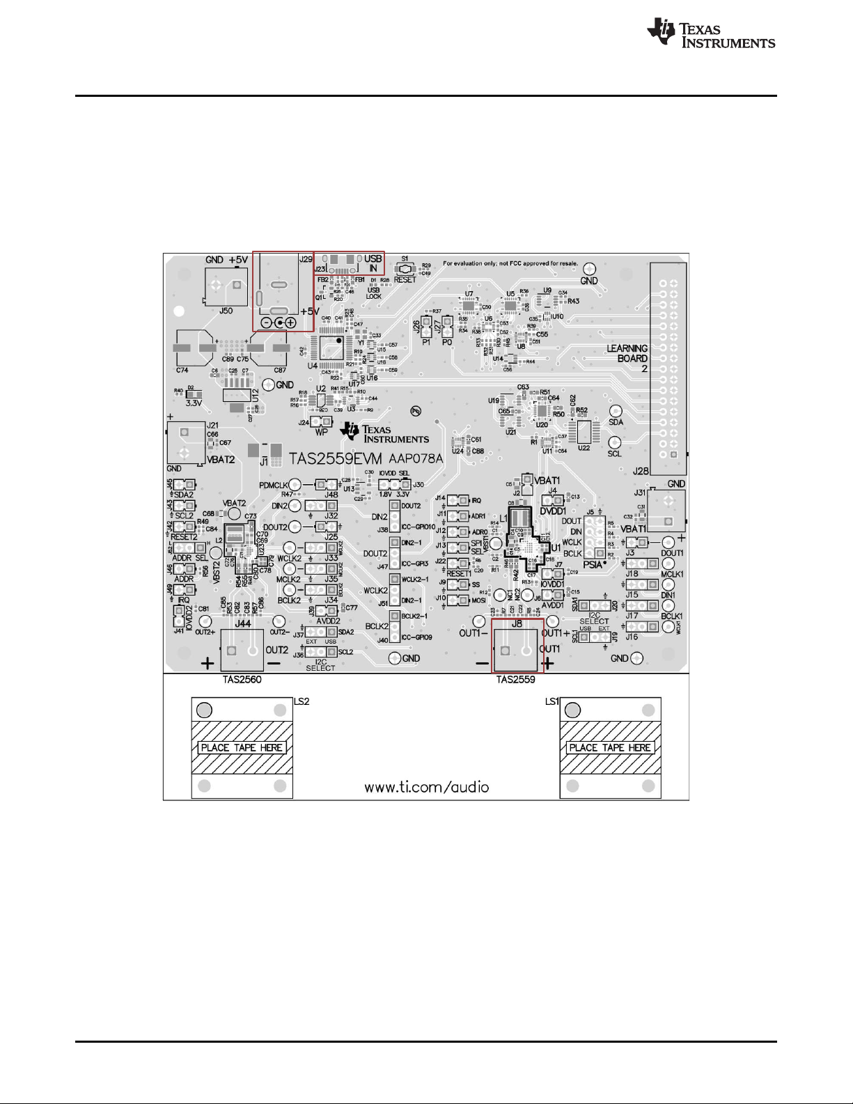
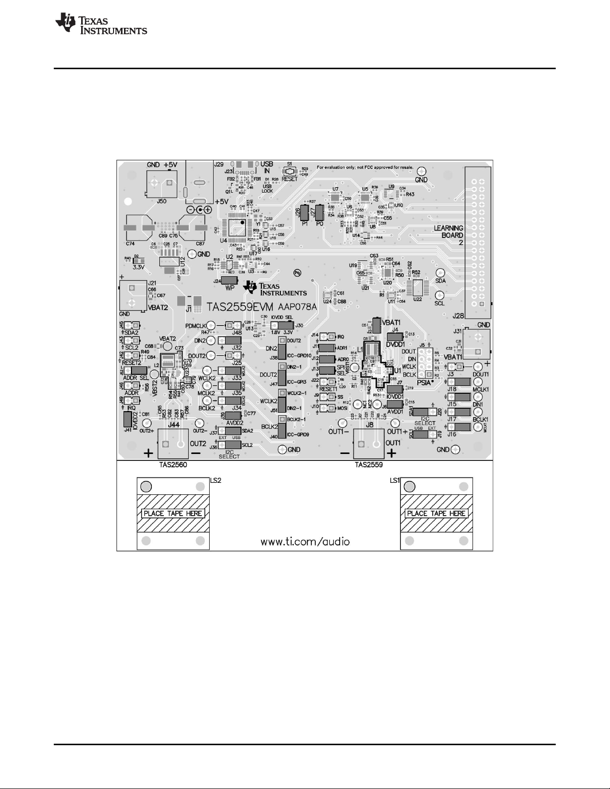
Mono Setup
4 Mono Setup
1. Install PurePath Console 3 with the TAS2559EVM plug-in.
2. Connect a speaker to J8 on the EVM.
3. Attach a 5.0 V/ 2.5 A power supply to connector J29 (inner = 5V, outer = GND).
4. Remove Jumpers J38, J47, J51, and J40.
5. Connect the EVM to a Windows 7+ PC with a micro-USB cable (J23). It will enumerate as a USBAudioEVM device (sound card).
www.ti.com
Figure 1. TAS2559 EVM Mono Setup
4
TAS2559 Evaluation Module
Copyright © 2016–2017, Texas Instruments Incorporated
SLOU462A–November 2016–Revised March 2017
Submit Documentation Feedback
Page 5
www.ti.com
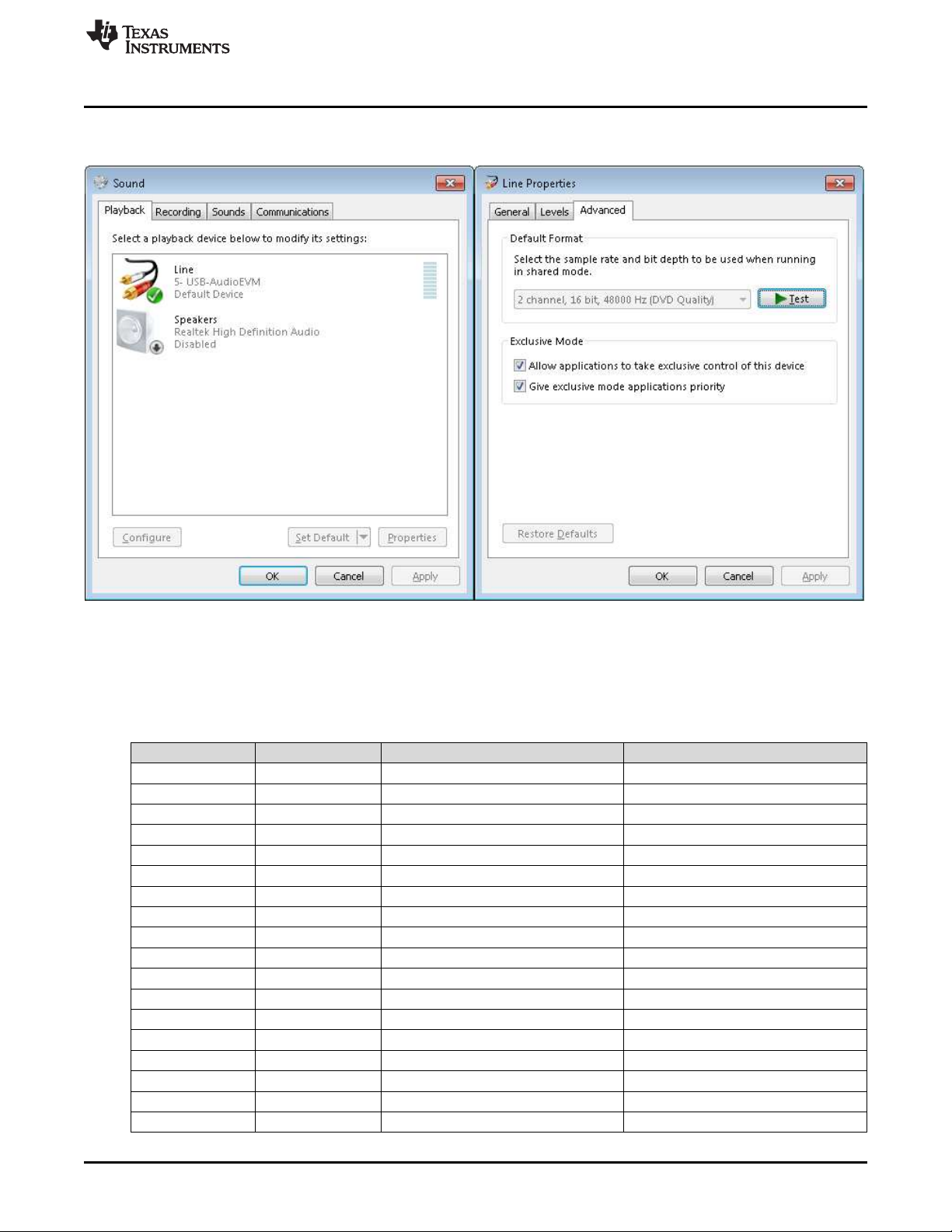
6. Verify that the EVM is the default playback device by opening the sound dialog from the Windows
Mono Setup
Control Panel as shown in Figure 2.
Figure 2. Setting Default Playback Device
7. Check if the sampling rate matches the Windows setting by opening the advanced tab in the properties
menu. The EVM firmware enumerates as a USB-AudioEVM that supports 48 kHz sampling rate by
default. This setting must match the EVM at 2-channel, 16-bit, 48000 Hz (CD Quality).
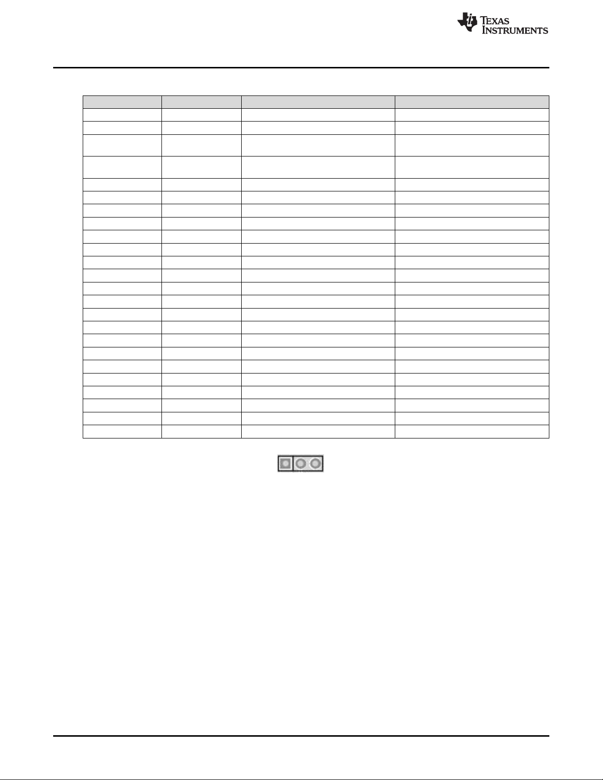
Table 2. Default Jumper Settings
JUMPER SETTING DESCRIPTION CHANNEL
J2 Insert VBAT 5V
J3 Remove DOUT 1
J4 Insert DVDD 1.8V 1
J6 Insert AVDD 1.8V 1
J7 Insert IOVDD Setting from J30 1
J9 Remove SCL / SS 1
J10 Remove SDA / MOSI 1
J11 Insert Address Select1 1
J12 Insert Address Select0 1
J13 Insert SPI Select 1
J14 Remove IRQ 1
J15 Pin 1-2 SDIN = on-board 1
J16 Pin 1-2 WCLK = on-board 1
J17 Pin 1-2 BCLK = on-board 1
J18 Pin 1-2 MCLK = on-board 1
J19 Pin 1-2 SCL = on-board 1
J20 Pin 1-2 SDA = on-board 1
J22 Remove Reset 1
SLOU462A–November 2016–Revised March 2017
Submit Documentation Feedback
Copyright © 2016–2017, Texas Instruments Incorporated
TAS2559 Evaluation Module
5
Page 6
1 2 3
Mono Setup
Table 2. Default Jumper Settings (continued)
JUMPER SETTING DESCRIPTION CHANNEL
J24 Insert WP = 1, write protect EEPROM
J25 Remove DOUT 2
J26 Insert
J27 Insert
J30 Pin 1-2 IOVDD Select = 3.3 V 2
J32 Pin 1-2 SDIN = on-board 2
J33 Pin 1-2 WCLK = on-board 2
J34 Pin 1-2 BCLK = on-board 2
J35 Pin 1-2 MCLK = on-board 2
J36 Pin 1-2 SCL = on-board 2
J37 Pin 1-2 SDA = on-board 2
J38 Pin 2-3 ICC =1, inter-chip communication 2
J39 Insert AVDD 1.8V 2
J40 Pin 2-3 ICC =1, inter-chip communication 2
J41 Insert IOVDD 2
J42 Remove Reset 2
J43 Remove SCL = on-board
J45 Remove SDA = on-board
J46 Remove Address Select0 2
J47 Pin 2-3 ICC =1, inter-chip communication 2
J48 Remove PDM CLK 2
J49 Remove IRQ 2
J51 Pin 2-3 ICC =1, inter-chip communication 2
J52 Pin 1-2 Address Select1 2
P1 = 0, select USB for on-board digital
audio
P0 = 0, select USB for on-board digital
audio
www.ti.com
Figure 3. 3-Pin Jumper
Please refer to Figure 5 for default jumper settings.
6
TAS2559 Evaluation Module
Copyright © 2016–2017, Texas Instruments Incorporated
SLOU462A–November 2016–Revised March 2017
Submit Documentation Feedback
Page 7

www.ti.com
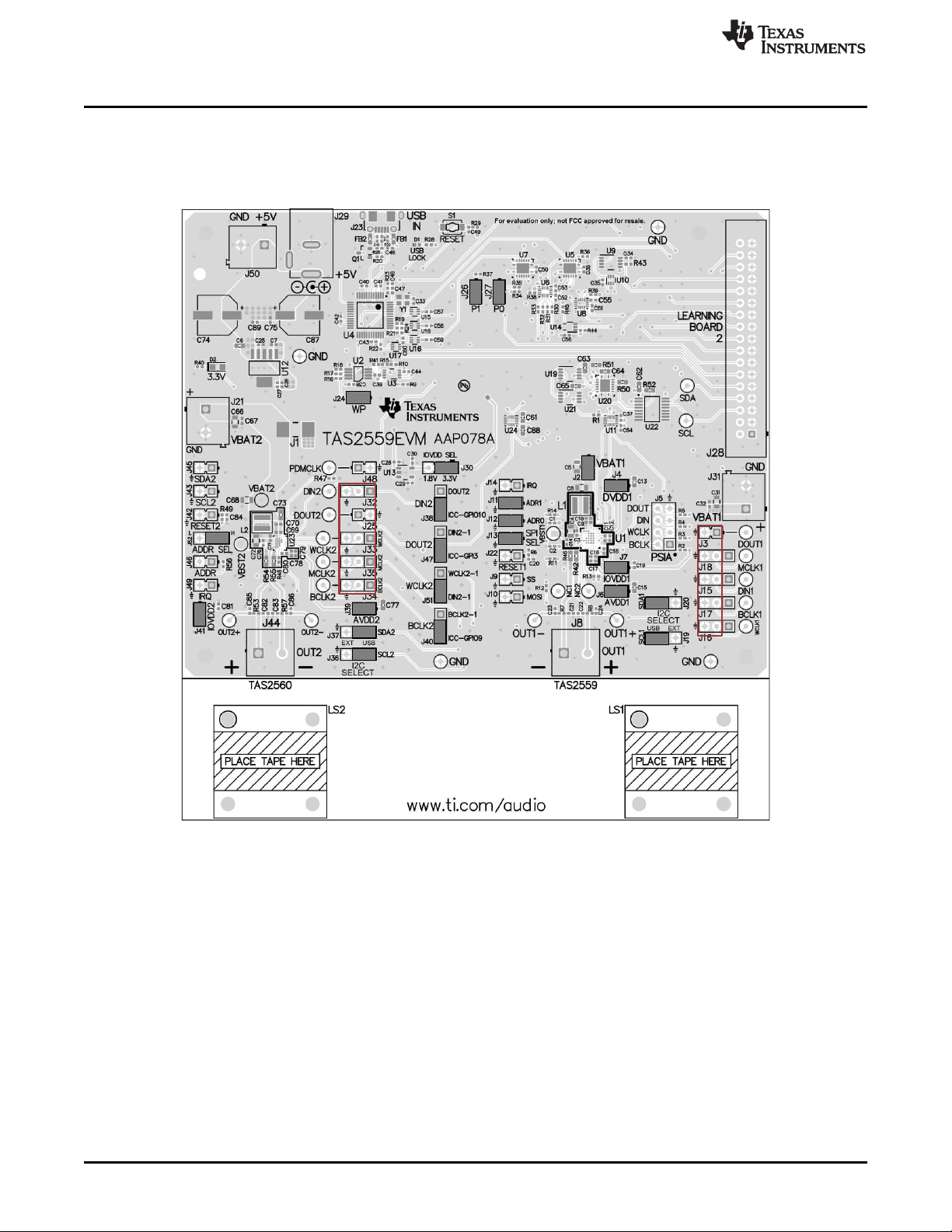
5 Stereo Setup
1. Install PurePath Console 3 with the TAS2559EVM plug-in.
2. Connect speakers to both J44 and J8 on the EVM.
3. Attach a 5.0 V/ 5.0 A power supply to connector J29 (inner = 5V, outer = GND).
4. Connect the EVM to a Windows 7+ PC with a micro-USB cable (J23). It will enumerate as a USBAudioEVM device (sound card).
Stereo Setup
Figure 4. TAS2559EVM Stereo Setup
5. Proceed with characterization per the PPC3 User’s guide.
6. Change to channel B in the device control pane and set to Right Channel.
7. Play the test tone as shown in Figure 2.
SLOU462A–November 2016–Revised March 2017
Submit Documentation Feedback
Copyright © 2016–2017, Texas Instruments Incorporated
TAS2559 Evaluation Module
7
Page 8

Digital Audio Interfaces
6 Digital Audio Interfaces
The various digital audio interfaces on the TAS2559EVM can be selected through hardware settings and
software settings. Several headers close to the TAS2559 device allow access to the following digital audio
signals:
• J3: Data Out (DOUT) from the TAS2559 (For example, current and voltage sense data.)
• J25: Data out (DOUT2) from the TAS2560
• J15: Data In (DIN) to the TAS2559
• J16: Word Clock or Frame Sync (WCLK)
• J17: Bit Clock (BCLK)
• J18: Master Clock (MCLK) (This is optional if TAS2559 PLL is not used.)
• J48: PDM Clock (PDMCLK) – optional input source for TAS2560
• J32: Data in (DIN2) to the TAS2650 – can be used for PDM input if desired
J3 has two pins:
• Digital data (for example, I and V sense data) from the TAS2559 device
• Ground
J15, J16, J17, and J18 have three pins:
• Digital audio signals from the EVM
• Digital audio signals to the TAS2559
• Ground
A jumper inserted in position 1-2 connects the TAS2559 to the digital audio signals from the board (for
example, USB or Learning Board 2). Replacing the jumper with a connector from an external source
connects the TAS2559 to the external source (for example, AP or PSIA).
The selection between the two on-board digital audio sources (USB or Learning Board 2) is controlled by:
(a) Hardware: J26,J27
• J26 = inserted, J27 = inserted; Selects USB
• J26 = inserted, J27 = removed; Selects Learning Board 2
(b) Software: The PPC3 GUI controls the digital audio routing during speaker characterization. This has
priority over the hardware settings from point a.
The secondary digital audio interface from the TAS2559 device is directly available through J5.
www.ti.com
8
TAS2559 Evaluation Module
Copyright © 2016–2017, Texas Instruments Incorporated
SLOU462A–November 2016–Revised March 2017
Submit Documentation Feedback
Page 9
www.ti.com
6.1 Digital Audio Interface Selection
6.1.1 USB
The TAS2559EVM contains a microcontroller (TAS1020B) that acts as a USB HID and USB-class audio
interface. To select USB, insert both J26 and J27 and insert J15, J16, J17, and J18 in the 1-2 position.
This is shown in Figure 5.
Digital Audio Interfaces
SLOU462A–November 2016–Revised March 2017
Submit Documentation Feedback
Copyright © 2016–2017, Texas Instruments Incorporated
Figure 5. USB Audio Selection
TAS2559 Evaluation Module
9
Page 10
Digital Audio Interfaces
6.1.2 Direct (AP/PSIA)
Remove the jumpers from J15, J16, J17 and J18 for Channel 1 (or J32, J33, J34, and J35 for Channel 2)
and connect the external digital audio source (for example AP or PSIA) to pin 2 of each head. Pin 3
provides a convenient ground connection. This is shown in Figure 6.
www.ti.com
10
TAS2559 Evaluation Module
Figure 6. Direct (AP/PSIA) Audio Selection
SLOU462A–November 2016–Revised March 2017
Copyright © 2016–2017, Texas Instruments Incorporated
Submit Documentation Feedback
Page 11

+3.3V
10.0k
R17
10.0k
R18
27.4
R27
27.4
R26
1.50k
R25
47pF
C46
47pF
C45
Q1
15.0k
R20
BlueD1
USB LOCK
360
R28
3.09k
R23
100pF
C47
1000pF C48
GND GND GND
GND
+3.3V
GND
GND
+3.3V
+3.3V
+3.3V
+3.3V +3.3V
100k
R29
GND
S1
+3.3V
USB RESET
MRESET
+3.3V
+5V-USB
PUR
DP
DM
0.1µF
16V
C35
0.1µF
16V
C36
0.1µF
16V
C37
0.1µF
16V
C38
0.1µF
16V
C39
0.1µF
16V
C49
0.1µF
16V
C43
MRESET
FB1
FB2
GND
GND
4.99k
R16
GND
+3.3V
TP12
SCL
TP13
SDA
SCL
SDA
I2C
2.00k
R9
DNP
DNP 2.00k
R10
DNP
DNP
SCL-USB
SDA-USB
0.1µF
16V
C33
0.1µF
16V
C34
0.1µF
16V
C40
0.1µF
16V
C41
0.1µF
16V
C42
IOVDD
0.1µF
16V
C44
GND
IOVDD
MCLK-USB
I2S-USB
49.9R19
49.9
R21
49.9
R22
49.9
R24
SDIN-USB
10.0k
R15
J24
WP
NC
1
NC
2
A2
3
VSS4SDA
5
SCL
6
WP
7
VCC
8
U2
24LC256-I/MS
VBUS
1
D-
2
D+
3
ID
4
GND
5
678
9
J23
USB-IN
6MHz
VCC
4
E/D
1
GND2OUT
3
Y1
SDA_B
1
GND
2
VCCA
3
SDA_A
4
SCL_A
5
OE
6
VCCB
7
SCL_B
8
U3
TCA9406DCUR
GND
USB_I2CEN
FROM LB2 CONN
+3.3V
USB_I2CEN IOVDD
IOVDD IOVDD
SCL-USB
SDA-USB
I2C-USB
0
R41
MCLK-USB
1A
1
GND
2
2A
3
2Y
4
VCC
5
1Y
6
U15
SN74LVC2G34DRLR
GND
+3.3V
1A
1
GND
2
2A
3
2Y
4
VCC
5
1Y
6
U16
SN74LVC2G34DRLR
1A
1
GND
2
2A
3
2Y
4
VCC
5
1Y
6
U17
SN74LVC2G34DRLR
1A
1
GND
2
2A
3
2Y
4
VCC
5
1Y
6
U18
SN74LVC2G34DRLR
MCLKIN-LB2
BCLKIN-LB2
LRCLKIN-LB2
SDIN0-LB2
I2S
LEARNING BOARD2
LRCLK-USB
BCLK-USB
SDOUT-USB
SDOUT-USB
BCLK-USB
LRCLK-USB
0.1µF
16V
C59
0.1µF
16V
C56
0.1µF
16V
C57
0.1µF
16V
C58
MCLKIN-LB2
SDIN0-LB2
BCLKIN-LB2
LRCLKIN-LB2
0.1µF
16V
C60
DECOUPLING
SCL-USB
SDA-USB
SDIN-USB
CSYNC
CSCLK
CDATO
MCLK01
PLLFILO
1
AVDD
2
MCLKI
3
DVSS
4
PUR
5
DP
6
DM
7
DVDD
8
MRESET
9
TEST
10
EXTEN
11
RSTO
12
P3-0
13
P3-1
14
P3-2/XINT
15
DVSS
16
P3-3
17
P3-4
18
P3-5
19
NC
20
DVDD
21
NC
22
P1-0
23
P1-1
24
P1-2
25
P1-3
26
P1-4
27
DVSS
28
P1-5
29
P1-6
30
P1-7
31
CSCHNE
32
DVDD
33
CSYNC
35
CDATI
36
CSCLK
37
CDATO
38
MCLKO1
39
MCLKO2
40
RESET
41
VREN
42
SDA
43
SCL
44
AVSS
45
XTALO
46
XTALI
47
PLLFILI
48
CRESET
34
U4
TAS1020BPFBR
GND
GND
www.ti.com
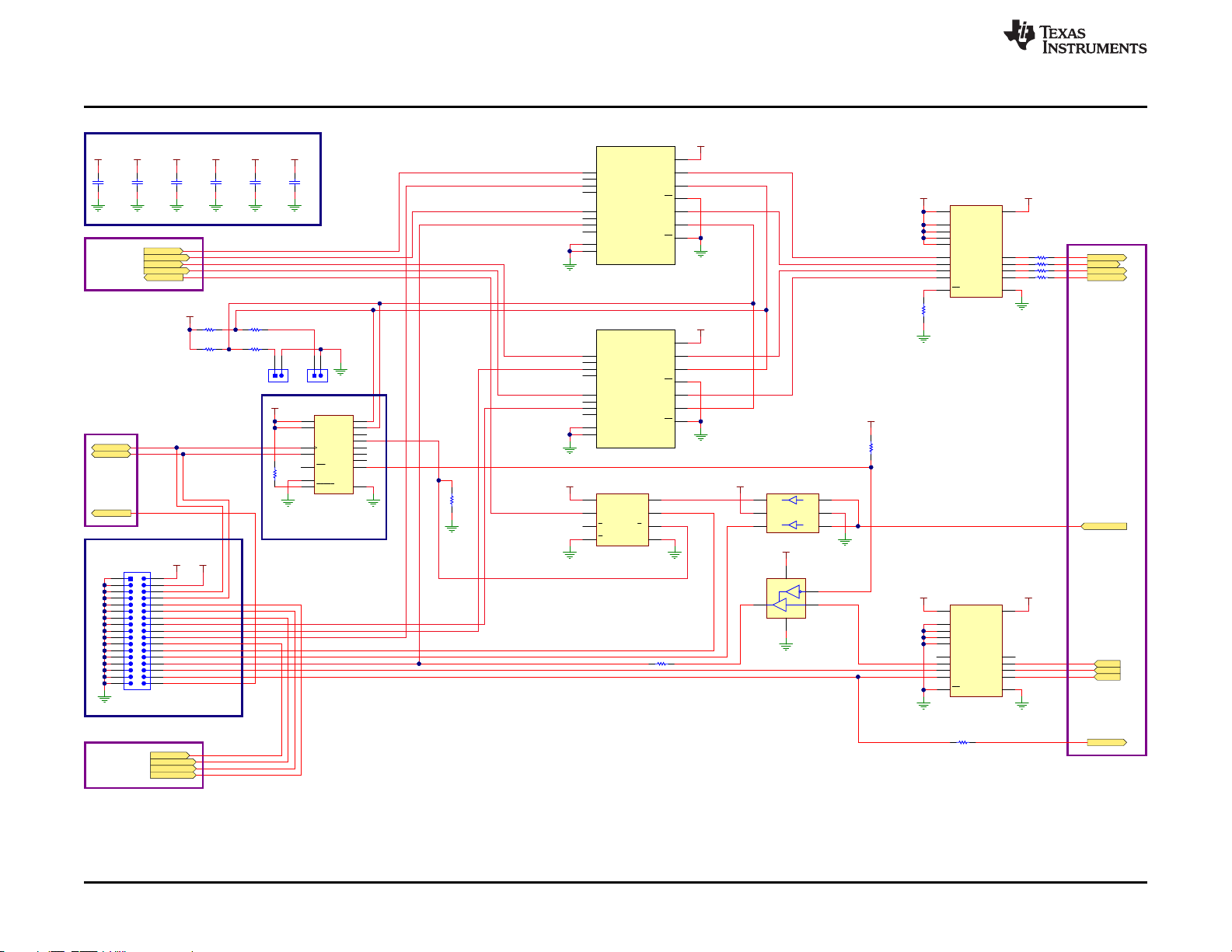
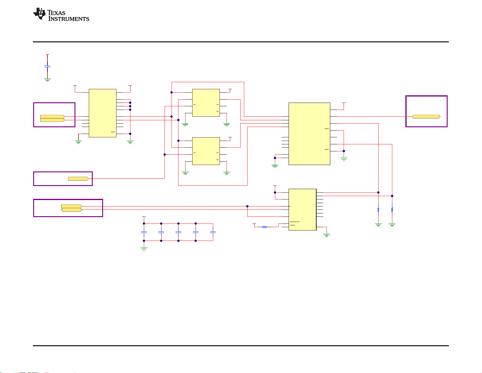
7 Hardware Documentation
7.1 TAS2559EVM Schematics
Figure 7 through Figure 12 show the schematics for the TAS2559 EVM.
Hardware Documentation
SLOU462A–November 2016–Revised March 2017
Submit Documentation Feedback
Figure 7. TAS2559EVM USB Block
Copyright © 2016–2017, Texas Instruments Incorporated
TAS2559 Evaluation Module
11
Page 12
GND
+5.0V
SCL-USB
SDA-USB
GND
GND
GND
IOVDD
10.0k
R38
0R33
0
R32
0R31
0
R30
MCLK
SCLK
LRCLK
SDIN
GND
MCLK
SDIN
SCLK
LRCLK
MCLK-USB
I2S-USB
SDOUT-USB
BCLK-USB
LRCLK-USB
MCLK-USB
SDOUT-USB
BCLK-USB
LRCLK-USB
WCLK-from-LB2
SDOUT3-from-LB2
BCLK-from-LB2
SDIN-USB
SDIN-USB
47k
R36
2.2k
R35
GND
47k
R34
2.2k
R37
GNDGND
1 2
3 4
5 6
7 8
9 10
11 12
13 14
15
17
19
21
23
25
27
29
31
16
18
20
22
24
26
28
30
32
33 34
J28
+3.3V
+3.3V
+3.3V
+3.3V
+3.3V
GND
+3.3V
GND
1A
1
GND
2
2A
3
2Y
4
VCC
5
1Y
6
U10
SN74LVC2G34DRLR
GND
+3.3V
A
1
B
2
Y
3
GND
4
Y
5
A/B
6
G
7
VCC
8
U9
SN74LVC2G157DCTR
RESET
1
P0
2
P1
3
P2
4
P3
5
GND
6
P4
7
P5
8
P6
9
P7
10
INT
11
SCL
12
SDA
13
VCCP
14
VCCI
15
ADDR
16
U8
TCA6408ARSVR
GNDGND
I2C
EXPANDER
DECOUPLING
0.1µF
C50
+3.3V
GND
0.1µF
C53
+3.3V
GND
0.1µF
C54
GND
0.1µF
C51
+3.3V
GND
0.1µF
C52
GND
IOVDD
DIR1
15
DIR2
16
A1
1
A2
2
A3
3
A4
4
DIR3
5
DIR4
6
OE7GND
8
B4
9
B3
10
B2
11
B1
12
VCCB
13
VCCA
14
U6
SN74AVC4T774RSVR
10.0k
R39
I2S/MIX-MUX
WCLK-DUT
BCLK-DUT
MCLK-DUT
DOUT-MIXMUX
DIN-DUT
I2C-USB
USB_I2CEN
USB_I2CEN
DIR1
15
DIR2
16
A1
1
A2
2
A3
3
A4
4
DIR3
5
DIR4
6
OE7GND
8
B4
9
B3
10
B2
11
B1
12
VCCB
13
VCCA
14
U11
SN74AVC4T774RSVR
GND GND
DIN1
BCLK1
WCLK1
IOVDD+3.3V
LRCLK-to-LB2
BCLK-to-LB2
LRCLK-to-LB2
BCLK-to-LB2
WCLK-from-LB2
BCLK-from-LB2
MCLK-from-LB2
SDOUT3-from-LB2
IOVDD
J26P1J27
P0
S1
2
1B1
6
1B2
5
1A
7
2B4
13
2B3
12
1B4
3
1B3
4
2B1
10
2B2
11
2A
9
GND
8
VCC
16
1OE
1
2OE
15
S0
14
EP
17
U5
SN74CB3Q3253RGYR
S1
2
1B1
6
1B2
5
1A
7
2B4
13
2B3
12
1B4
3
1B3
4
2B1
10
2B2
11
2A
9
GND
8
VCC
16
1OE
1
2OE
15
S0
14
EP
17
U7
SN74CB3Q3253RGYR
10.0k
R43
GND
0.1µF
C55
GND
IOVDD
1
2
3
4
5
U14 SN74LVC1G125DCKR
+3.3V
GND
49.9R45SDOUT3-from-LB2
10.0k
R44
+3.3V
MCLKIN-LB2
SDIN0-LB2
BCLKIN-LB2
LRCLKIN-LB2
LRCLK-to-LB2
BCLK-to-LB2
+3.3V
SCL-USB
SDA-USB
I2S
LEARNING
BOARD 2
MCLKIN-LB2
SDIN0-LB2
BCLKIN-LB2
LRCLKIN-LB2
MCLK-from-LB2
SDOUT1-from-LB2
SDIN2-to-LB2
SDOUT1-from-LB2
SDIN2-to-LB2
SDOUT1-from-LB2
49.9
R1
LRCLK-MM
Hardware Documentation
www.ti.com
Figure 8. TAS2559EVM Input Muxes and Translators
12
TAS2559 Evaluation Module
Copyright © 2016–2017, Texas Instruments Incorporated
SLOU462A–November 2016–Revised March 2017
Submit Documentation Feedback
Page 13
GND
GND
GND
10k
R50
10k
R51
0.1µF
C61
0.1µF
C62
0.1µF
C63
0.1µF
C64
GND
0.1µF
C65
GND
GND
A
1
B
2
Y
3
GND
4
Y
5
A/B
6
G
7
VCC
8
U19
SN74LVC2G157DCTR
A
1
B
2
Y
3
GND
4
Y
5
A/B
6
G
7
VCC
8
U21
SN74LVC2G157DCTR
S1
2
1B1
6
1B2
5
1A
7
2B4
13
2B3
12
1B4
3
1B3
4
2B1
10
2B2
11
2A
9
GND
8
VCC
16
1OE
1
2OE
15
S0
14
EP
17
U20
SN74CB3Q3253RGYR
GND GND
GND
+3.3V
+3.3V
+3.3V
+3.3V
+3.3V
SDATA-MM1
SDATA-MM2
SCL-USB
SDA-USB
LRCLK-MM
SCL-USB
SDA-USB
I2C-USB
DOUT-MIXMUX
RESET
3
P0
4
P1
5
P2
6
P3
7
GND
8
P4
9
P5
10
P6
11
P7
12
IRQ
13
SCL
14
SDA
15
VCCP
16
VCC
1
A0
2
U22
XRA1206IG16-F
10k
R52
+3.3V
TO
SCL-USB
GND
SDATA-MM1
SDATA-MM2
DOUT-MIXMUX
DIR1
15
DIR2
16
A1
1
A2
2
A3
3
A4
4
DIR3
5
DIR4
6
OE
7
GND
8
B4
9
B3
10
B2
11
B1
12
VCCB13VCCA
14
U24
SN74AVC4T774RSVR
GNDGND
IOVDD +3.3V
From LB2
LRCLK-MM
DOUT-DUT2
DOUT-DUT1
From DUTS LB2/USB
0.1µF
C88
GND
IOVDD
www.ti.com
Hardware Documentation
SLOU462A–November 2016–Revised March 2017
Submit Documentation Feedback
Figure 9. TAS2559EVM Output Muxes and Translators
TAS2559 Evaluation Module
Copyright © 2016–2017, Texas Instruments Incorporated
13
Page 14

INM1
GND
BCLK2-1
WCLK2-1
DIN2-1
RESET1
10.0k
R6
IOVDD
GND
ADR1-1_MISO
ADR0-1_SCLK
SPI_SELECT1
IRQ_GPIO4-1
RESET1
SPI-SEL
ADR
IRQ
IOVDD
ADR1-1_MISO
ADR0-1_SCLK
SPI_SELECT1
IRQ_GPIO4-1
GND
MOSI
SS
SCL1_SS
SDA1_MOSI
ASI2
ASI1
10.0k
R2
IOVDD
10.0k
R3
IOVDD
10.0k
R4
IOVDD
10.0k
R5
IOVDD
GND
DOUT2-1
1 2
3 4
5 6
7 8
J5
PSIA
123
J15
123
J16
123
J17
123
J18
123
J19
123
J20
ICC-GPI3
ICC-GPIO10
ICC-GPIO9
BCLK2-1
WCLK2-1
DIN2-1
DOUT2-1
GND
MCLK1
BCLK1
WCLK1
DIN1
DOUT-DUT1
SCL
SDA
I2C
I2S
TP6
GND
GND
TP7
GND
GND
LB2
CONN
DIN1
BCLK1
WCLK1
J9
J10
J11
J12
J13
J14
SCL1_SS
SDA1_MOSI
J3
10.0k
R11
10.0k
R12
10.0k
R13
10.0k
R14
WCLK-DUT
BCLK-DUT
MCLK-DUT
DIN-DUT
J22
RESET1
0.1µF
C20
GND
DOUT-DUT1
MIX
MUX
VBAT1
0.1µF
C11
1µF
C12
10µF
C13
GND GND GND
+1.8V
J4
DVDD1
0.1µF
C16
1µF
C17
10µF
C15
DNP
DNP
GND GND GND
+1.8V
J6
AVDD1
DVDD1
AVDD1
1µF
C19
0.1µF
C18
GND GND
IOVDD
J7
IOVDD1
IOVDD1
DIN1
BCLK1
DOUT-DUT1
MCLK1
WCLK1
TP1
MCLK1
TP2
BCLK1
TP3
WCLK1
TP4
DIN1
TP5
DOUT1
TP10
NC1
TP11
NC2
0.1µFC1
0.1µFC2
INP1
TO
DUT2
DIN-DUT2
BCLK-DUT2
WCLK-DUT2
MCLK1
123
J51
WCLK2
123
J47
DOUT2
123
J40
BCLK2
123
J38
DIN2
DOUT-DUT2
PGND_B
A1
PGND_B
A2
VBAT
A3
ICC_GPIO9
A4
WCLK1_GPIO2
A5
DOUT1_GPIO3
A6
SW
B1
SW
B2
ICC_GPIO10
B3
ICC_GPI3
B4
DIN1_GPI1
B5
BCLK1_GPIO1
B6
VBOOST
C1
VBOOST
C2
INP
C3
DGND
C4
DIN2_GPIO8
C5
DVDD
C6
SPK_M
D1
VREG
D2
INM
D3
IOGND
D4
IRQ_GPIO4
D5
MCLK_GPI2
D6
PGND
E1
VSENSE_P
E2
AGND
E3
SDA_MOSI
E4
WCLK2_GPIO6
E5
DOUT2_GPIO7
E6
SPK_P
F1
VSENSE_M
F2
SCL_SSZ
F3
AVDD
F4
ADR0_SCLK
F5
BCLK2_GPIO5
F6
NC2
G1
NC1
G2
ADR1_MISO
G3
SPI_SELECT
G4
RESET
G5
IOVDD
G6
U1
TAS2559YZR
OUT1+
OUT1-
ASI1
MCLK1
BCLK1
WCLK1
DIN1
DOUT-DUT1
GND GND
GND GND
GND
+5.0V
SPEAKER
OUT
GND
VBAT1
GND
DNP
VBOOST1
SPK1+
SPK1-
SW1
SW1
DIN1
BCLK1
DOUT-DUT1
MCLK1
WCLK1
1000pF
C21
DNP
DNP
GND
1.00k
R7
DNP
DNP
4700pF
C23
DNP
DNP
GND
TP8
OUT1-
DNP
DNP
GND
1000pF
C22
DNP
DNP
1.00k
R8
DNP
DNP
4700pF
C24
DNP
DNP
GND
TP9
OUT1+
DNP
DNP
1
2
J8
OUT1
0
R42
0
R46
0.01µF
C14
0.1µF
16V
C3
TP14
VBST1
22µF
16V
C4
2.2uH
L1
0.1µFC91µF
C10
J2
VBAT1
22µF
16V
C5
22µF
16V
C8
ICC-GPI3
ICC-GPIO9
ICC-GPIO10
DIN2-1
TO
DUT2
Hardware Documentation
14
TAS2559 Evaluation Module
Figure 10. TAS2559EVM Channel 1 Schematic
Copyright © 2016–2017, Texas Instruments Incorporated
www.ti.com
SLOU462A–November 2016–Revised March 2017
Submit Documentation Feedback
Page 15

0.1µF
C69
1µF
C70
2.2uH
L2
0.01µF
C76
1000pF
C82
DNP
DNP
GND
GND GND
GND GND
GND
0.1µF
C78
1µF
C79
10µF
C77
DNP
DNP
GNDGNDGND
GND
IOVDD
ADDR
IRQ
GND
0.1µF
16V
C71
1000pF
C83
DNP
DNP
SCL2
SDA2
+1.8V
TP15
VBST2
SPEAKER
OUT
22µF
16V
C72
1.00k
R53
DNP
DNP
4700pF
C85
DNP
DNP
GND
1.00k
R57
DNP
DNP
4700pF
C86
DNP
DNP
GND
TP25
OUT2+
DNP
TP26
OUT2-
DNP
MCLK1-2
BCLK1-2
WCLK1-2
DIN1-2
DOUT-DUT2
GND
22µF
C68
123
J32
DIN2
123
J33
WCLK2
123
J34
BCLK2
123
J35
MCLK2
123
J36
SCL2
123
J37
SDA2
TP16
MCLK2
TP17
BCLK2
TP18
WCLK2
TP19
DIN2
TP20
DOUT2
GND
MCLK1-2
BCLK1-2
WCLK1-2
DIN1-2
DOUT-DUT2
SCL
SDA
I2C
TP21
GND
GND
TP22
GND
GND
J39
AVDD2
J43
SCL2
J45
SDA2
J46
ADDR
J49
IRQ
J25
DOUT2
1
2
J44
OUT2
0
R54
0
R55
DNP DNP
22.1kR56
10.0k
R48
ADDR
IRQ
SCL2
SDA2
GND
RESET2
10.0k
R49
IOVDD
RESET2
J42
RESET2
0.1µF
C84
GND
DOUT-DUT2
MIX
MUX
SW2
VBAT2
TP27
VBAT2
MCLK
B1
BCLK
D2
WCLK
C1
DIN
D1
DOUT
E2
SCL
E3
SDA
F2
ADDR
A1
IRQ
A3
RESETZ
F1
NC2
B2
NC1
C2
SW
E4
SW
E5
VBOOST
D4
VBOOST
D5
VBAT
F3
AVDD
B3
IOVDD
A2
VREG
C4
SPK_P
C5
SPK_N
A5
VSENSE_P
A4
VSENSE_N
B4
GND
D3
GND
C3
PGND_B
F5
PGND_B
F4
PGND
B5
PDMCLK
E1
U23
TAS2560YFFR
VBOOST2
SPK2+
SPK2-
1µF
C81
0.1µF
C80
GND GND
IOVDD
J41
IOVDD2
IOVDD2
AVDD2
10.0k
R47
GND
TP23
PDMCLK
GND
J48
PDMCLK
10µF
C73
GND
OUT2+
OUT2-
FROM
TAS2559
DIN-DUT2
BCLK-DUT2
WCLK-DUT2
MCLK1
1
2
3
J52
ADDR SEL
GND
IOVDD
www.ti.com
SLOU462A–November 2016–Revised March 2017
Submit Documentation Feedback
Figure 11. TAS2559EVM Channel 2 (TAS2560) Schematic
Copyright © 2016–2017, Texas Instruments Incorporated
Hardware Documentation
TAS2559 Evaluation Module
15
Page 16

C25
IN
1
2
EN3NR
4
OUT
5
GND
U13
TPS73618DBVR
1µF
C7
0.1µF
C27
10µF
C6
1µF
C28
0.1µF
C30
0.01µF
C29
+3.3V
+1.8V
360
R40
GND
Green
D2
3.3V
GND
GND
GND
GND
GND
GND
GND
GND
GND
GND
+1.8V
+3.3V
IOVDD
1
3
2
J29
+5V
+5.0V
IN1OUT
2
3
NR
4
EN
5
6
GND
U12
TPS73733DCQ
1µF
C26
GND
+5V
123
J30
IOVDD SEL
+3.3V
VBAT
VBAT1
0.1µF
10V
C32
GND
22µF
16V
C31
GND
GND
J31
VBAT1
VBAT2
0.1µF
10V
C67
GND
22µF
16V
C66
GND
GND
J21
VBAT2
VBAT1 VBAT2
Hi Current Shunt
J1
J50
+5V
GND
100µF
C74
GND
100µF
C87
GND
0.1µF
C89
GND
0.1µF
C75
GND
Hardware Documentation
www.ti.com
16
TAS2559 Evaluation Module
Figure 12. TAS2559EVM Power Supply
SLOU462A–November 2016–Revised March 2017
Submit Documentation Feedback
Copyright © 2016–2017, Texas Instruments Incorporated
Page 17
www.ti.com
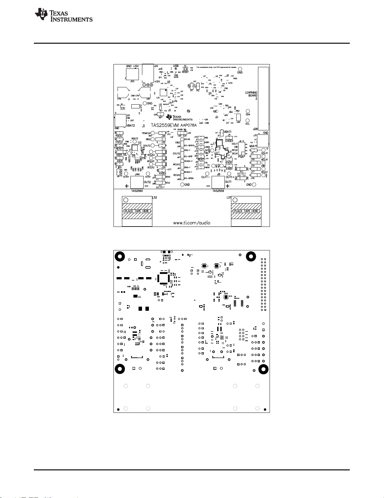
7.2 TAS2559 EVM Printed Circuit Board Layout
Hardware Documentation
Figure 13. Top Overlay
SLOU462A–November 2016–Revised March 2017
Submit Documentation Feedback
Copyright © 2016–2017, Texas Instruments Incorporated
Figure 14. Top Solder Mask
TAS2559 Evaluation Module
17
Page 18

Hardware Documentation
www.ti.com
Figure 15. Top Layer
18
TAS2559 Evaluation Module
Figure 16. Copper Layer 2
SLOU462A–November 2016–Revised March 2017
Copyright © 2016–2017, Texas Instruments Incorporated
Submit Documentation Feedback
Page 19

www.ti.com
Hardware Documentation
Figure 17. Copper Layer 3
SLOU462A–November 2016–Revised March 2017
Submit Documentation Feedback
Copyright © 2016–2017, Texas Instruments Incorporated
Figure 18. Copper Layer 4
TAS2559 Evaluation Module
19
Page 20
Hardware Documentation
www.ti.com
Figure 19. Copper Layer 5
20
TAS2559 Evaluation Module
Figure 20. Bottom Layer
SLOU462A–November 2016–Revised March 2017
Copyright © 2016–2017, Texas Instruments Incorporated
Submit Documentation Feedback
Page 21

www.ti.com
Hardware Documentation
Figure 21. Bottom Solder Mask
SLOU462A–November 2016–Revised March 2017
Submit Documentation Feedback
Copyright © 2016–2017, Texas Instruments Incorporated
Figure 22. Drill Drawing
TAS2559 Evaluation Module
21
Page 22

Hardware Documentation
www.ti.com
Figure 23. Board Dimensions
22
TAS2559 Evaluation Module
SLOU462A–November 2016–Revised March 2017
Copyright © 2016–2017, Texas Instruments Incorporated
Submit Documentation Feedback
Page 23

www.ti.com
7.3 TAS2559EVM Bill of Materials
DESIGNATOR QTY VALUE DESCRIPTION PACKAGE REFERENCE PART NUMBER MANUFACTURER
!PCB 1 Printed Circuit Board AAP078 Any - -
C1, C2, C9, C11, C16, C18, C20, C27, C30,
C32, C50, C51, C52, C53, C54, C55, C67,
C69, C75, C78, C80, C84, C89
C3, C71 2 0.1uF
C4, C5, C8, C31, C66, C68, C72 7 22uF
C6, C13, C15, C73 4 10uF
C7, C10, C12, C17, C19, C26, C28, C70, C79,
C33, C34, C35, C36, C37, C38, C39, C40,
C41, C42, C43, C44, C49, C56, C57, C58,
C61, C62, C63, C64, C65, C88 6 0.1uF
C81
C14, C25, C29, C76 4 0.01uF
C21, C22, C48 3 1000pF
C23, C24 2 4700pF
C59, C60
C45, C46 2 47pF
C47 1 100pF
C74, C87 2 100uF
D1 1 Blue LED, Blue, SMD Blue LED SMLP12BC7TT86 Rohm - D2 1 Green LED, Green, SMD LED_0805 LTST-C171GKT Lite-On - -
FB1, FB2 2 220 ohm
H1, H2, H3, H4 4
H5, H6, H7, H8 4
H9 1
H10 1
J1 1 JUMPER TIN SMD 6.85x0.97x2.51 mm S1911-46R Harwin - -
23 0.1uF
10 1uF
18 0.1uF
Table 3. TAS2559EVM Bill of Materials
CAP, CERM, 0.1uF, 10V, +/10%, X7R, 0402
CAP, CERM, 0.1 µF, 16 V, +/10%, X7R, 0402
CAP, CERM, 22 µF, 16 V, +/10%, X5R, 0805
CAP, CERM, 10 µF, 10 V, +/20%, X5R, 0603
CAP, CERM, 1 µF, 6.3 V, +/20%, X5R, 0402
CAP, CERM, 0.01uF, 6.3V,
+/-10%, X7R, 0402
CAP, CERM, 1000pF, 50V,
+/-5%, C0G/NP0, 0402
CAP, CERM, 4700 pF, 50 V,
+/- 10%, X7R, 0402
CAP, CERM, 0.1uF, 16V, +/10%, X7R, 0402
CAP, CERM, 47pF, 25V, +/5%, C0G/NP0, 0402
CAP, CERM, 100pF, 50V, +/5%, C0G/NP0, 0402
CAP, CERM, 0.1 µF, 25 V, +/5%, X7R, 0603
CAP, AL, 100 µF, 16 V, +/20%, 0.4 ohm, SMD
2.2A Ferrite Bead, 220 ohm
@ 100MHz, SMD
Machine Screw, Round, #4-40
x 1/4, Nylon, Philips panhead
Standoff, Hex, 0.5"L #4-40
Nylon
Custom Cable For Connecting
Stereo EVM Boards. IDC34
Ribbon Cable With Offset
Pins.
Double Sided Tape for
Applying Speakers to Boards
Hardware Documentation
ALTERNATE PART
NUMBER
0402
0402
0805
0603
0402
0402
0402
0402
0402
0402
0402
0603 06033C104JAT2A AVX - -
SMT Radial E EEE-FC1C101P Panasonic - -
0603 MPZ1608S221A TDK - -
Screw NY PMS 440 0025 PH B&F Fastener Supply - -
Standoff 1902C Keystone - -
IDC34 Custom Cable CBL007 Any Shop - -
Double Sided Tape 1/2-5-9495LE 3M (TC) - -
GRM155R71A104KA0
1D
GRM155R71C104KA8
8D
C2012X5R1C226K125
AC
C1608X5R1A106M08
0AC
C1005X5R0J105M050
BB
GRM155R70J103KA0
1D
GRM1555C1H102JA0
1D
GRM155R71H472KA0
1D
GRM155R71C104KA8
8D
GRM1555C1E470JA0
1D
GRM1555C1H101JA0
1D
MuRata - -
MuRata - -
TDK - -
TDK - -
TDK - -
MuRata - -
MuRata - -
MuRata - -
MuRata - -
MuRata - -
MuRata - -
ALTERNATE
MANUFACTURER
SLOU462A–November 2016–Revised March 2017
Submit Documentation Feedback
Copyright © 2016–2017, Texas Instruments Incorporated
TAS2559 Evaluation Module
23
Page 24

Hardware Documentation
DESIGNATOR QTY VALUE DESCRIPTION PACKAGE REFERENCE PART NUMBER MANUFACTURER
J2, J3, J4, J6, J7, J9, J10, J11, J12, J13, J14,
J22, J24, J25, J26, J27, J39, J41, J42, J43,
J15, J16, J17, J18, J19, J20, J32, J33, J34,
R2, R3, R4, R5, R6, R11, R12, R13, R14, R15,
J45, J46, J48, J49
J5 1 Header, 100mil, 4x2, Tin, TH Header, 4x2, 100mil, Tin PEC04DAAN Sullins Connector Solutions - -
J8, J44 2
J35, J36, J37, J38, J40, J47, J51, J52
J21, J31, J50 3
J23 1
J28 1
J29 1
J30 1
L1, L2 2 2.2uH
LS1, LS2 2 Dynamic Speaker 9x16mm SPS0916B-J-01 AAC Technologies - -
Q1 1 0.3V
R1, R19, R21, R22, R24, R45 6 49.9
R38, R39, R43, R44, R47, R48, R49
R7, R8 2 1.00k
R16 1 4.99k
R17, R18 2 10.0k
R20 1 15.0k
R23 1 3.09k
R25 1 1.50k
R26, R27 2 27.4
R28, R40 2 360
R29 1 100k
R30, R31, R32, R33 4 0
24
17 1x3
17 10.0k
Table 3. TAS2559EVM Bill of Materials (continued)
Header, 2.54 mm, 2x1, Tin,
TH
Terminal Block, 5.08mm, 2x1,THTerminal Block, 5.08mm,
Header, 100mil, 3x1, Gold,
TH
Terminal Block, 5 mm, 2x1,
Tin, TH
Connector, Receptacle,
Micro-USB Type AB, R/A,
Bottom Mount SMT
Header (shrouded), 2.54 mm,
17x2, Gold, TH
Power Jack, mini, 2.5mm OD,
R/A, TH
Header, 2.54 mm, 3x1, Tin,
TH
Inductor, Shielded,
Composite, 2.2uH, 3.7A, 0.02
ohm, SMD
Transistor, NPN, 40V, 0.15A,
SOT-23
RES, 49.9 ohm, 1%, 0.063W,
0402
RES, 10.0k ohm, 1%,
0.063W, 0402
RES, 1.00 k, 1%, 0.063 W,
0402
RES, 4.99k ohm, 1%,
0.063W, 0402
RES, 10.0 k, 1%, 0.063 W,
0402
RES, 15.0k ohm, 1%,
0.063W, 0402
RES, 3.09k ohm, 1%,
0.063W, 0402
RES, 1.50k ohm, 1%,
0.063W, 0402
RES, 27.4 ohm, 1%, 0.063W,
0402
RES, 360 ohm, 5%, 0.063W,
0402
RES, 100k ohm, 1%, 0.063W,
0402
RES, 0 ohm, 5%, 0.063W,
0402
Header, 2.54 mm, 2x1, TH TSW-102-07-T-S Samtec - -
2x1, TH
PBC03SAAN PBC03SAAN SullinsConnector Solutions - Terminal Block, 5 mm, 2x1,
TH
Connector, USB Micro AB DX4R205JJAR1800 JAE Electronics - -
Header (shrouded), 2.54
mm, 17x2, TH
Jack, 14.5x11x9mm RAPC712X Switchcraft - -
Header, 2.54 mm, 3x1, TH TSW-103-07-T-S Samtec - -
4x2x4mm XFL4020-222MEB Coilcraft - -
SOT-23 MMBT2222A Fairchild Semiconductor - -
0402
0402
0402
0402
0402
0402
0402
0402
0402
0402
0402
0402 CRCW04020000Z0ED Vishay-Dale - -
0395443002 Molex - -
691 101 710 002 Wurth Elektronik eiSos - -
N2534-6002-RB 3M - -
CRCW040249R9FKE
D
CRCW040210K0FKE
D
CRCW04021K00FKE
D
CRCW04024K99FKE
D
CRCW040210K0FKE
D
CRCW040215K0FKE
D
CRCW04023K09FKE
D
CRCW04021K50FKE
D
CRCW040227R4FKE
D
CRCW0402360RJNE
D
CRCW0402100KFKE
D
ALTERNATE PART
NUMBER
Vishay-Dale - -
Vishay-Dale - -
Vishay-Dale - -
Vishay-Dale - -
Vishay-Dale - -
Vishay-Dale - -
Vishay-Dale - -
Vishay-Dale - -
Vishay-Dale - -
Vishay-Dale - -
Vishay-Dale - -
ALTERNATE
MANUFACTURER
www.ti.com
24
TAS2559 Evaluation Module
SLOU462A–November 2016–Revised March 2017
Submit Documentation Feedback
Copyright © 2016–2017, Texas Instruments Incorporated
Page 25

www.ti.com
DESIGNATOR QTY VALUE DESCRIPTION PACKAGE REFERENCE PART NUMBER MANUFACTURER
R34, R36 2 47k
R35, R37 2 2.2k
R41 1 0 RES, 0, 5%, 0.063 W, 0402 0402 CRCW04020000Z0ED Vishay-Dale - -
R42, R46, R54, R55 4 0 RES, 0, 5%, 0.1 W, 0603 0603 CRCW06030000Z0EA Vishay-Dale - -
R50, R51, R52 3 10k RES, 10 k, 5%, 0.1 W, 0603 0603
R56 1 22.1k
S1 1
SH1, SH2, SH3, SH4, SH5, SH6, SH7, SH8,
SH9, SH10, SH11, SH12, SH13, SH14,
SH15,SH16, SH17, SH18, SH19, SH20, SH21,
SH22, SH23, SH24, SH25, SH26, SH27,
SH28,SH29, SH30, SH31, SH32, SH33, SH34,
TP1, TP2, TP3, TP4, TP5, TP8, TP9, TP10,
TP11, TP12, TP13, TP14, TP15, TP16, TP17,
SH35, SH36, SH37
TP18, TP19, TP20, TP23, TP25, TP26
TP6, TP7, TP21, TP22 4 Black
TP27 1
U1 1
U2 1
U3 1
U4 1 TAS1020BPFB IC, USB Streaming Controller PQFP48 TAS1020BPFB TI - None
U5, U7, U20 3
U6, U11, U24 3
37 1x2
21 Orange
Table 3. TAS2559EVM Bill of Materials (continued)
RES, 47 k, 5%, 0.063 W,
0402
RES, 2.2 k, 5%, 0.063 W,
0402
RES, 22.1 k, 1%, 0.063 W,
0402
Switch, Tactile, SPST-NO,
0.05A, 12V, SMT
Shunt, 100mil, Gold plated,
Black
Test Point, Miniature, Orange,
TH
Test Point, Miniature, Black,
TH
Test Point, Miniature, Red,
TH
5.7-W Class-D Mono Audio
Amplifier with Class-H Boost
and Speaker Sense with
Stereo Processing, YZ0042C01 (DSBGA-42)
EEPROM, 256KBIT, 400KHZ,
MSOP8
TCA9406 Dual Bidirectional 1MHz I2C-BUS and SMBus
Voltage Level-Translator, 1.65
to 3.6 V, -40 to 85 degC, 8pin US8 (DCU), Green (RoHS
& no Sb/Br)
Dual 1-of-4 FET Multiplexer /
Demultiplexer 2.5-V / 3.3-V
Low-Voltage High-Bandwidth
Bus Switch, RGY0016A
4-BIT DUAL-SUPPLY BUS
TRANSCEIVER WITH
CONFIGURABLE VOLTAGE
TRANSLATION AND 3STATE OUTPUTS,
RSV0016A
0402
0402
0402
Switch, 4.4x2x2.9 mm TL1015AF160QG E-Switch - -
Shunt SNT-100-BK-G Samtec 969102-0000-DA 3M
Orange Miniature Testpoint 5003 Keystone - -
Black Miniature Testpoint 5001 Keystone - -
Red Miniature Testpoint 5000 Keystone - -
YZ0042-C01 TAS2559YZR TexasInstruments - Texas Instruments
MSOP-8 24LC256-I/MS Microchip - -
DCU0008A TCA9406DCUR Texas Instruments Equivalent Texas Instruments
RGY0016A
RSV0016A SN74AVC4T774RSVR Texas Instruments - None
CRCW040247K0JNE
D
CRCW04022K20JNE
D
CRCW060310K0JNE
A
CRCW040222K1FKE
D
SN74CB3Q3253RGY
R
Hardware Documentation
ALTERNATE PART
NUMBER
Vishay-Dale - -
Vishay-Dale - -
Vishay-Dale - -
Vishay-Dale - -
Texas Instruments - Texas Instruments
ALTERNATE
MANUFACTURER
SLOU462A–November 2016–Revised March 2017
Submit Documentation Feedback
Copyright © 2016–2017, Texas Instruments Incorporated
TAS2559 Evaluation Module
25
Page 26
Hardware Documentation
DESIGNATOR QTY VALUE DESCRIPTION PACKAGE REFERENCE PART NUMBER MANUFACTURER
U8 1
U9, U19, U21 3
U10, U15, U16, U17, U18 5
U12 1
U13 1
U14 1
U22 1
U23 1
Y1 1 Oscillator, 6MHz, 3.3V, SMD 2.5x1x2.5mm 625L3I006M00000 CTS Electrocomponents - -
C77 0 10uF
C82, C83 0 1000pF
C85, C86 0 4700pF
FID1, FID2, FID3 0
R9, R10 0 2.00k
R53, R57 0 1.00k
Table 3. TAS2559EVM Bill of Materials (continued)
Low-Voltage 8-Bit I2C and
SMBus I/O Expander, 1.65 to
5.5 V, -40 to 85 degC, 16-pin
UQFN (RSV), Green (RoHS &
no Sb/Br)
Single 2-Line to 1-Line Data
Selector Multiplexer,
DCT0008A
DUAL BUFFER GATE,
DRL0006A
Single Output LDO, 1 A,
Fixed 3.3 V Output, 2.2 to 5.5
V Input, with Reverse Current
Protection, 6-pin SOT-223
(DCQ), -40 to 125 degC,
Green (RoHS & no Sb/Br)
Single Output Low Noise
LDO, 400 mA, Fixed 1.8 V
Output, 1.7 to 5.5 V Input,
with Reverse Current
Protection, 5-pin SOT-23
(DBV), -40 to 85 degC, Green
(RoHS & no Sb/Br)
Single Bus Buffer Gate With
3-State Output, DCK0005A
8-BIT I2C/SMBUS GPIO
EXPANDER WITH
INTEGRATED LEVEL
SHIFTERS, TSSOP-16
5.6-W Class-D Mono Audio
Amplifier with IV Sense,
YFF0030-C01
CAP, CERM, 10 µF, 10 V, +/20%, X5R, 0603
CAP, CERM, 1000pF, 50V,
+/-5%, C0G/NP0, 0402
CAP, CERM, 4700 pF, 50 V,
+/- 10%, X7R, 0402
Fiducial mark. There is
nothing to buy or mount.
RES, 2.00 k, 1%, 0.063 W,
0402
RES, 1.00 k, 1%, 0.063 W,
0402
RSV0016A TCA6408ARSVR Texas Instruments Equivalent None
DCT0008A
DRL0006A SN74LVC2G34DRLR Texas Instruments - None
DCQ0006A TPS73733DCQ Texas Instruments Equivalent None
DBV0005A TPS73618DBVR Texas Instruments Equivalent None
DCK0005A
4.5x1.2x5.1 mm XRA1206IG16-F Exar - -
YFF0030-C01 TAS2560YFFR Texas Instruments TAS2560YFFT Texas Instruments
0603
0402
0402
Fiducial N/A N/A - -
0402
0402
SN74LVC2G157DCT
R
SN74LVC1G125DCK
R
C1608X5R1A106M08
0AC
GRM1555C1H102JA0
1D
GRM155R71H472KA0
1D
CRCW04022K00FKE
D
CRCW04021K00FKE
D
www.ti.com
ALTERNATE PART
NUMBER
Texas Instruments -
Texas Instruments SN74LVC1G125DCKT Texas Instruments
TDK - -
MuRata - -
MuRata - -
Vishay-Dale - -
Vishay-Dale - -
ALTERNATE
MANUFACTURER
None, Texas Instruments,
Texas Instruments
26
TAS2559 Evaluation Module
SLOU462A–November 2016–Revised March 2017
Submit Documentation Feedback
Copyright © 2016–2017, Texas Instruments Incorporated
Page 27

www.ti.com
NOTE: Page numbers for previous revisions may differ from page numbers in the current version.
Changes from Original (November 2016) to A Revision ................................................................................................ Page
• Changed Figure 1 ......................................................................................................................... 4
• Changed Figure 4 ......................................................................................................................... 7
• Changed Figure 5 ......................................................................................................................... 9
• Changed Figure 6........................................................................................................................ 10
SLOU462A–November 2016–Revised March 2017
Submit Documentation Feedback
Copyright © 2016–2017, Texas Instruments Incorporated
Revision History
27
Page 28

STANDARD TERMS FOR EVALUATION MODULES
1. Delivery: TI delivers TI evaluation boards, kits, or modules, including any accompanying demonstration software, components, and/or
documentation which may be provided together or separately (collectively, an “EVM” or “EVMs”) to the User (“User”) in accordance
with the terms set forth herein. User's acceptance of the EVM is expressly subject to the following terms.
1.1 EVMs are intended solely for product or software developers for use in a research and development setting to facilitate feasibility
evaluation, experimentation, or scientific analysis of TI semiconductors products. EVMs have no direct function and are not
finished products. EVMs shall not be directly or indirectly assembled as a part or subassembly in any finished product. For
clarification, any software or software tools provided with the EVM (“Software”) shall not be subject to the terms and conditions
set forth herein but rather shall be subject to the applicable terms that accompany such Software
1.2 EVMs are not intended for consumer or household use. EVMs may not be sold, sublicensed, leased, rented, loaned, assigned,
or otherwise distributed for commercial purposes by Users, in whole or in part, or used in any finished product or production
system.
2 Limited Warranty and Related Remedies/Disclaimers:
2.1 These terms do not apply to Software. The warranty, if any, for Software is covered in the applicable Software License
Agreement.
2.2 TI warrants that the TI EVM will conform to TI's published specifications for ninety (90) days after the date TI delivers such EVM
to User. Notwithstanding the foregoing, TI shall not be liable for a nonconforming EVM if (a) the nonconformity was caused by
neglect, misuse or mistreatment by an entity other than TI, including improper installation or testing, or for any EVMs that have
been altered or modified in any way by an entity other than TI, (b) the nonconformity resulted from User's design, specifications
or instructions for such EVMs or improper system design, or (c) User has not paid on time. Testing and other quality control
techniques are used to the extent TI deems necessary. TI does not test all parameters of each EVM.
User's claims against TI under this Section 2 are void if User fails to notify TI of any apparent defects in the EVMs within ten (10)
business days after delivery, or of any hidden defects with ten (10) business days after the defect has been detected.
2.3 TI's sole liability shall be at its option to repair or replace EVMs that fail to conform to the warranty set forth above, or credit
User's account for such EVM. TI's liability under this warranty shall be limited to EVMs that are returned during the warranty
period to the address designated by TI and that are determined by TI not to conform to such warranty. If TI elects to repair or
replace such EVM, TI shall have a reasonable time to repair such EVM or provide replacements. Repaired EVMs shall be
warranted for the remainder of the original warranty period. Replaced EVMs shall be warranted for a new full ninety (90) day
warranty period.
3 Regulatory Notices:
3.1 United States
3.1.1 Notice applicable to EVMs not FCC-Approved:
FCC NOTICE: This kit is designed to allow product developers to evaluate electronic components, circuitry, or software
associated with the kit to determine whether to incorporate such items in a finished product and software developers to write
software applications for use with the end product. This kit is not a finished product and when assembled may not be resold or
otherwise marketed unless all required FCC equipment authorizations are first obtained. Operation is subject to the condition
that this product not cause harmful interference to licensed radio stations and that this product accept harmful interference.
Unless the assembled kit is designed to operate under part 15, part 18 or part 95 of this chapter, the operator of the kit must
operate under the authority of an FCC license holder or must secure an experimental authorization under part 5 of this chapter.
3.1.2 For EVMs annotated as FCC – FEDERAL COMMUNICATIONS COMMISSION Part 15 Compliant:
CAUTION
This device complies with part 15 of the FCC Rules. Operation is subject to the following two conditions: (1) This device may not
cause harmful interference, and (2) this device must accept any interference received, including interference that may cause
undesired operation.
Changes or modifications not expressly approved by the party responsible for compliance could void the user's authority to
operate the equipment.
FCC Interference Statement for Class A EVM devices
NOTE: This equipment has been tested and found to comply with the limits for a Class A digital device, pursuant to part 15 of
the FCC Rules. These limits are designed to provide reasonable protection against harmful interference when the equipment is
operated in a commercial environment. This equipment generates, uses, and can radiate radio frequency energy and, if not
installed and used in accordance with the instruction manual, may cause harmful interference to radio communications.
Operation of this equipment in a residential area is likely to cause harmful interference in which case the user will be required to
correct the interference at his own expense.
Page 29

FCC Interference Statement for Class B EVM devices
NOTE: This equipment has been tested and found to comply with the limits for a Class B digital device, pursuant to part 15 of
the FCC Rules. These limits are designed to provide reasonable protection against harmful interference in a residential
installation. This equipment generates, uses and can radiate radio frequency energy and, if not installed and used in accordance
with the instructions, may cause harmful interference to radio communications. However, there is no guarantee that interference
will not occur in a particular installation. If this equipment does cause harmful interference to radio or television reception, which
can be determined by turning the equipment off and on, the user is encouraged to try to correct the interference by one or more
of the following measures:
• Reorient or relocate the receiving antenna.
• Increase the separation between the equipment and receiver.
• Connect the equipment into an outlet on a circuit different from that to which the receiver is connected.
• Consult the dealer or an experienced radio/TV technician for help.
3.2 Canada
3.2.1 For EVMs issued with an Industry Canada Certificate of Conformance to RSS-210 or RSS-247
Concerning EVMs Including Radio Transmitters:
This device complies with Industry Canada license-exempt RSSs. Operation is subject to the following two conditions:
(1) this device may not cause interference, and (2) this device must accept any interference, including interference that may
cause undesired operation of the device.
Concernant les EVMs avec appareils radio:
Le présent appareil est conforme aux CNR d'Industrie Canada applicables aux appareils radio exempts de licence. L'exploitation
est autorisée aux deux conditions suivantes: (1) l'appareil ne doit pas produire de brouillage, et (2) l'utilisateur de l'appareil doit
accepter tout brouillage radioélectrique subi, même si le brouillage est susceptible d'en compromettre le fonctionnement.
Concerning EVMs Including Detachable Antennas:
Under Industry Canada regulations, this radio transmitter may only operate using an antenna of a type and maximum (or lesser)
gain approved for the transmitter by Industry Canada. To reduce potential radio interference to other users, the antenna type
and its gain should be so chosen that the equivalent isotropically radiated power (e.i.r.p.) is not more than that necessary for
successful communication. This radio transmitter has been approved by Industry Canada to operate with the antenna types
listed in the user guide with the maximum permissible gain and required antenna impedance for each antenna type indicated.
Antenna types not included in this list, having a gain greater than the maximum gain indicated for that type, are strictly prohibited
for use with this device.
Concernant les EVMs avec antennes détachables
Conformément à la réglementation d'Industrie Canada, le présent émetteur radio peut fonctionner avec une antenne d'un type et
d'un gain maximal (ou inférieur) approuvé pour l'émetteur par Industrie Canada. Dans le but de réduire les risques de brouillage
radioélectrique à l'intention des autres utilisateurs, il faut choisir le type d'antenne et son gain de sorte que la puissance isotrope
rayonnée équivalente (p.i.r.e.) ne dépasse pas l'intensité nécessaire à l'établissement d'une communication satisfaisante. Le
présent émetteur radio a été approuvé par Industrie Canada pour fonctionner avec les types d'antenne énumérés dans le
manuel d’usage et ayant un gain admissible maximal et l'impédance requise pour chaque type d'antenne. Les types d'antenne
non inclus dans cette liste, ou dont le gain est supérieur au gain maximal indiqué, sont strictement interdits pour l'exploitation de
l'émetteur
3.3 Japan
3.3.1 Notice for EVMs delivered in Japan: Please see http://www.tij.co.jp/lsds/ti_ja/general/eStore/notice_01.page 日本国内に
輸入される評価用キット、ボードについては、次のところをご覧ください。
http://www.tij.co.jp/lsds/ti_ja/general/eStore/notice_01.page
3.3.2 Notice for Users of EVMs Considered “Radio Frequency Products” in Japan: EVMs entering Japan may not be certified
by TI as conforming to Technical Regulations of Radio Law of Japan.
If User uses EVMs in Japan, not certified to Technical Regulations of Radio Law of Japan, User is required to follow the
instructions set forth by Radio Law of Japan, which includes, but is not limited to, the instructions below with respect to EVMs
(which for the avoidance of doubt are stated strictly for convenience and should be verified by User):
1. Use EVMs in a shielded room or any other test facility as defined in the notification #173 issued by Ministry of Internal
Affairs and Communications on March 28, 2006, based on Sub-section 1.1 of Article 6 of the Ministry’s Rule for
Enforcement of Radio Law of Japan,
2. Use EVMs only after User obtains the license of Test Radio Station as provided in Radio Law of Japan with respect to
EVMs, or
3. Use of EVMs only after User obtains the Technical Regulations Conformity Certification as provided in Radio Law of Japan
with respect to EVMs. Also, do not transfer EVMs, unless User gives the same notice above to the transferee. Please note
that if User does not follow the instructions above, User will be subject to penalties of Radio Law of Japan.
Page 30

【無線電波を送信する製品の開発キットをお使いになる際の注意事項】 開発キットの中には技術基準適合証明を受けて
いないものがあります。 技術適合証明を受けていないもののご使用に際しては、電波法遵守のため、以下のいずれかの
措置を取っていただく必要がありますのでご注意ください。
1. 電波法施行規則第6条第1項第1号に基づく平成18年3月28日総務省告示第173号で定められた電波暗室等の試験設備でご使用
いただく。
2. 実験局の免許を取得後ご使用いただく。
3. 技術基準適合証明を取得後ご使用いただく。
なお、本製品は、上記の「ご使用にあたっての注意」を譲渡先、移転先に通知しない限り、譲渡、移転できないものとします。
上記を遵守頂けない場合は、電波法の罰則が適用される可能性があることをご留意ください。 日本テキサス・イ
ンスツルメンツ株式会社
東京都新宿区西新宿6丁目24番1号
西新宿三井ビル
3.3.3 Notice for EVMs for Power Line Communication: Please see http://www.tij.co.jp/lsds/ti_ja/general/eStore/notice_02.page
電力線搬送波通信についての開発キットをお使いになる際の注意事項については、次のところをご覧ください。http:/
/www.tij.co.jp/lsds/ti_ja/general/eStore/notice_02.page
3.4 European Union
3.4.1 For EVMs subject to EU Directive 2014/30/EU (Electromagnetic Compatibility Directive):
This is a class A product intended for use in environments other than domestic environments that are connected to a
low-voltage power-supply network that supplies buildings used for domestic purposes. In a domestic environment this
product may cause radio interference in which case the user may be required to take adequate measures.
4 EVM Use Restrictions and Warnings:
4.1 EVMS ARE NOT FOR USE IN FUNCTIONAL SAFETY AND/OR SAFETY CRITICAL EVALUATIONS, INCLUDING BUT NOT
LIMITED TO EVALUATIONS OF LIFE SUPPORT APPLICATIONS.
4.2 User must read and apply the user guide and other available documentation provided by TI regarding the EVM prior to handling
or using the EVM, including without limitation any warning or restriction notices. The notices contain important safety information
related to, for example, temperatures and voltages.
4.3 Safety-Related Warnings and Restrictions:
4.3.1 User shall operate the EVM within TI’s recommended specifications and environmental considerations stated in the user
guide, other available documentation provided by TI, and any other applicable requirements and employ reasonable and
customary safeguards. Exceeding the specified performance ratings and specifications (including but not limited to input
and output voltage, current, power, and environmental ranges) for the EVM may cause personal injury or death, or
property damage. If there are questions concerning performance ratings and specifications, User should contact a TI
field representative prior to connecting interface electronics including input power and intended loads. Any loads applied
outside of the specified output range may also result in unintended and/or inaccurate operation and/or possible
permanent damage to the EVM and/or interface electronics. Please consult the EVM user guide prior to connecting any
load to the EVM output. If there is uncertainty as to the load specification, please contact a TI field representative.
During normal operation, even with the inputs and outputs kept within the specified allowable ranges, some circuit
components may have elevated case temperatures. These components include but are not limited to linear regulators,
switching transistors, pass transistors, current sense resistors, and heat sinks, which can be identified using the
information in the associated documentation. When working with the EVM, please be aware that the EVM may become
very warm.
4.3.2 EVMs are intended solely for use by technically qualified, professional electronics experts who are familiar with the
dangers and application risks associated with handling electrical mechanical components, systems, and subsystems.
User assumes all responsibility and liability for proper and safe handling and use of the EVM by User or its employees,
affiliates, contractors or designees. User assumes all responsibility and liability to ensure that any interfaces (electronic
and/or mechanical) between the EVM and any human body are designed with suitable isolation and means to safely
limit accessible leakage currents to minimize the risk of electrical shock hazard. User assumes all responsibility and
liability for any improper or unsafe handling or use of the EVM by User or its employees, affiliates, contractors or
designees.
4.4 User assumes all responsibility and liability to determine whether the EVM is subject to any applicable international, federal,
state, or local laws and regulations related to User’s handling and use of the EVM and, if applicable, User assumes all
responsibility and liability for compliance in all respects with such laws and regulations. User assumes all responsibility and
liability for proper disposal and recycling of the EVM consistent with all applicable international, federal, state, and local
requirements.
5. Accuracy of Information: To the extent TI provides information on the availability and function of EVMs, TI attempts to be as accurate
as possible. However, TI does not warrant the accuracy of EVM descriptions, EVM availability or other information on its websites as
accurate, complete, reliable, current, or error-free.
Page 31

6. Disclaimers:
6.1 EXCEPT AS SET FORTH ABOVE, EVMS AND ANY MATERIALS PROVIDED WITH THE EVM (INCLUDING, BUT NOT
LIMITED TO, REFERENCE DESIGNS AND THE DESIGN OF THE EVM ITSELF) ARE PROVIDED "AS IS" AND "WITH ALL
FAULTS." TI DISCLAIMS ALL OTHER WARRANTIES, EXPRESS OR IMPLIED, REGARDING SUCH ITEMS, INCLUDING BUT
NOT LIMITED TO ANY EPIDEMIC FAILURE WARRANTY OR IMPLIED WARRANTIES OF MERCHANTABILITY OR FITNESS
FOR A PARTICULAR PURPOSE OR NON-INFRINGEMENT OF ANY THIRD PARTY PATENTS, COPYRIGHTS, TRADE
SECRETS OR OTHER INTELLECTUAL PROPERTY RIGHTS.
6.2 EXCEPT FOR THE LIMITED RIGHT TO USE THE EVM SET FORTH HEREIN, NOTHING IN THESE TERMS SHALL BE
CONSTRUED AS GRANTING OR CONFERRING ANY RIGHTS BY LICENSE, PATENT, OR ANY OTHER INDUSTRIAL OR
INTELLECTUAL PROPERTY RIGHT OF TI, ITS SUPPLIERS/LICENSORS OR ANY OTHER THIRD PARTY, TO USE THE
EVM IN ANY FINISHED END-USER OR READY-TO-USE FINAL PRODUCT, OR FOR ANY INVENTION, DISCOVERY OR
IMPROVEMENT, REGARDLESS OF WHEN MADE, CONCEIVED OR ACQUIRED.
7. USER'S INDEMNITY OBLIGATIONS AND REPRESENTATIONS. USER WILL DEFEND, INDEMNIFY AND HOLD TI, ITS
LICENSORS AND THEIR REPRESENTATIVES HARMLESS FROM AND AGAINST ANY AND ALL CLAIMS, DAMAGES, LOSSES,
EXPENSES, COSTS AND LIABILITIES (COLLECTIVELY, "CLAIMS") ARISING OUT OF OR IN CONNECTION WITH ANY
HANDLING OR USE OF THE EVM THAT IS NOT IN ACCORDANCE WITH THESE TERMS. THIS OBLIGATION SHALL APPLY
WHETHER CLAIMS ARISE UNDER STATUTE, REGULATION, OR THE LAW OF TORT, CONTRACT OR ANY OTHER LEGAL
THEORY, AND EVEN IF THE EVM FAILS TO PERFORM AS DESCRIBED OR EXPECTED.
8. Limitations on Damages and Liability:
8.1 General Limitations. IN NO EVENT SHALL TI BE LIABLE FOR ANY SPECIAL, COLLATERAL, INDIRECT, PUNITIVE,
INCIDENTAL, CONSEQUENTIAL, OR EXEMPLARY DAMAGES IN CONNECTION WITH OR ARISING OUT OF THESE
TERMS OR THE USE OF THE EVMS , REGARDLESS OF WHETHER TI HAS BEEN ADVISED OF THE POSSIBILITY OF
SUCH DAMAGES. EXCLUDED DAMAGES INCLUDE, BUT ARE NOT LIMITED TO, COST OF REMOVAL OR
REINSTALLATION, ANCILLARY COSTS TO THE PROCUREMENT OF SUBSTITUTE GOODS OR SERVICES, RETESTING,
OUTSIDE COMPUTER TIME, LABOR COSTS, LOSS OF GOODWILL, LOSS OF PROFITS, LOSS OF SAVINGS, LOSS OF
USE, LOSS OF DATA, OR BUSINESS INTERRUPTION. NO CLAIM, SUIT OR ACTION SHALL BE BROUGHT AGAINST TI
MORE THAN TWELVE (12) MONTHS AFTER THE EVENT THAT GAVE RISE TO THE CAUSE OF ACTION HAS
OCCURRED.
8.2 Specific Limitations. IN NO EVENT SHALL TI'S AGGREGATE LIABILITY FROM ANY USE OF AN EVM PROVIDED
HEREUNDER, INCLUDING FROM ANY WARRANTY, INDEMITY OR OTHER OBLIGATION ARISING OUT OF OR IN
CONNECTION WITH THESE TERMS, , EXCEED THE TOTAL AMOUNT PAID TO TI BY USER FOR THE PARTICULAR
EVM(S) AT ISSUE DURING THE PRIOR TWELVE (12) MONTHS WITH RESPECT TO WHICH LOSSES OR DAMAGES ARE
CLAIMED. THE EXISTENCE OF MORE THAN ONE CLAIM SHALL NOT ENLARGE OR EXTEND THIS LIMIT.
9. Return Policy. Except as otherwise provided, TI does not offer any refunds, returns, or exchanges. Furthermore, no return of EVM(s)
will be accepted if the package has been opened and no return of the EVM(s) will be accepted if they are damaged or otherwise not in
a resalable condition. If User feels it has been incorrectly charged for the EVM(s) it ordered or that delivery violates the applicable
order, User should contact TI. All refunds will be made in full within thirty (30) working days from the return of the components(s),
excluding any postage or packaging costs.
10. Governing Law: These terms and conditions shall be governed by and interpreted in accordance with the laws of the State of Texas,
without reference to conflict-of-laws principles. User agrees that non-exclusive jurisdiction for any dispute arising out of or relating to
these terms and conditions lies within courts located in the State of Texas and consents to venue in Dallas County, Texas.
Notwithstanding the foregoing, any judgment may be enforced in any United States or foreign court, and TI may seek injunctive relief
in any United States or foreign court.
Mailing Address: Texas Instruments, Post Office Box 655303, Dallas, Texas 75265
Copyright © 2017, Texas Instruments Incorporated
Page 32

IMPORTANT NOTICE FOR TI DESIGN INFORMATION AND RESOURCES
Texas Instruments Incorporated (‘TI”) technical, application or other design advice, services or information, including, but not limited to,
reference designs and materials relating to evaluation modules, (collectively, “TI Resources”) are intended to assist designers who are
developing applications that incorporate TI products; by downloading, accessing or using any particular TI Resource in any way, you
(individually or, if you are acting on behalf of a company, your company) agree to use it solely for this purpose and subject to the terms of
this Notice.
TI’s provision of TI Resources does not expand or otherwise alter TI’s applicable published warranties or warranty disclaimers for TI
products, and no additional obligations or liabilities arise from TI providing such TI Resources. TI reserves the right to make corrections,
enhancements, improvements and other changes to its TI Resources.
You understand and agree that you remain responsible for using your independent analysis, evaluation and judgment in designing your
applications and that you have full and exclusive responsibility to assure the safety of your applications and compliance of your applications
(and of all TI products used in or for your applications) with all applicable regulations, laws and other applicable requirements. You
represent that, with respect to your applications, you have all the necessary expertise to create and implement safeguards that (1)
anticipate dangerous consequences of failures, (2) monitor failures and their consequences, and (3) lessen the likelihood of failures that
might cause harm and take appropriate actions. You agree that prior to using or distributing any applications that include TI products, you
will thoroughly test such applications and the functionality of such TI products as used in such applications. TI has not conducted any
testing other than that specifically described in the published documentation for a particular TI Resource.
You are authorized to use, copy and modify any individual TI Resource only in connection with the development of applications that include
the TI product(s) identified in such TI Resource. NO OTHER LICENSE, EXPRESS OR IMPLIED, BY ESTOPPEL OR OTHERWISE TO
ANY OTHER TI INTELLECTUAL PROPERTY RIGHT, AND NO LICENSE TO ANY TECHNOLOGY OR INTELLECTUAL PROPERTY
RIGHT OF TI OR ANY THIRD PARTY IS GRANTED HEREIN, including but not limited to any patent right, copyright, mask work right, or
other intellectual property right relating to any combination, machine, or process in which TI products or services are used. Information
regarding or referencing third-party products or services does not constitute a license to use such products or services, or a warranty or
endorsement thereof. Use of TI Resources may require a license from a third party under the patents or other intellectual property of the
third party, or a license from TI under the patents or other intellectual property of TI.
TI RESOURCES ARE PROVIDED “AS IS” AND WITH ALL FAULTS. TI DISCLAIMS ALL OTHER WARRANTIES OR
REPRESENTATIONS, EXPRESS OR IMPLIED, REGARDING TI RESOURCES OR USE THEREOF, INCLUDING BUT NOT LIMITED TO
ACCURACY OR COMPLETENESS, TITLE, ANY EPIDEMIC FAILURE WARRANTY AND ANY IMPLIED WARRANTIES OF
MERCHANTABILITY, FITNESS FOR A PARTICULAR PURPOSE, AND NON-INFRINGEMENT OF ANY THIRD PARTY INTELLECTUAL
PROPERTY RIGHTS.
TI SHALL NOT BE LIABLE FOR AND SHALL NOT DEFEND OR INDEMNIFY YOU AGAINST ANY CLAIM, INCLUDING BUT NOT
LIMITED TO ANY INFRINGEMENT CLAIM THAT RELATES TO OR IS BASED ON ANY COMBINATION OF PRODUCTS EVEN IF
DESCRIBED IN TI RESOURCES OR OTHERWISE. IN NO EVENT SHALL TI BE LIABLE FOR ANY ACTUAL, DIRECT, SPECIAL,
COLLATERAL, INDIRECT, PUNITIVE, INCIDENTAL, CONSEQUENTIAL OR EXEMPLARY DAMAGES IN CONNECTION WITH OR
ARISING OUT OF TI RESOURCES OR USE THEREOF, AND REGARDLESS OF WHETHER TI HAS BEEN ADVISED OF THE
POSSIBILITY OF SUCH DAMAGES.
You agree to fully indemnify TI and its representatives against any damages, costs, losses, and/or liabilities arising out of your noncompliance with the terms and provisions of this Notice.
This Notice applies to TI Resources. Additional terms apply to the use and purchase of certain types of materials, TI products and services.
These include; without limitation, TI’s standard terms for semiconductor products http://www.ti.com/sc/docs/stdterms.htm), evaluation
modules, and samples (http://www.ti.com/sc/docs/sampterms.htm).
Mailing Address: Texas Instruments, Post Office Box 655303, Dallas, Texas 75265
Copyright © 2017, Texas Instruments Incorporated
Page 33

Mouser Electronics
Authorized Distributor
Click to View Pricing, Inventory, Delivery & Lifecycle Information:
Texas Instruments:
TAS2559EVM
 Loading...