

Page 1

TAS2505 Application Reference Guide
Reference Guide
Literature Number: SLAU472
February 2013
Page 2

TAS2505 Device Overview
• Chapter 1: Device Overview
• Chapter 2: TAS2505 Application
• Chapter 3: Device Initialization
• Chapter 4: Example Setups
• Chapter 5: Register Map and Descriptions
space
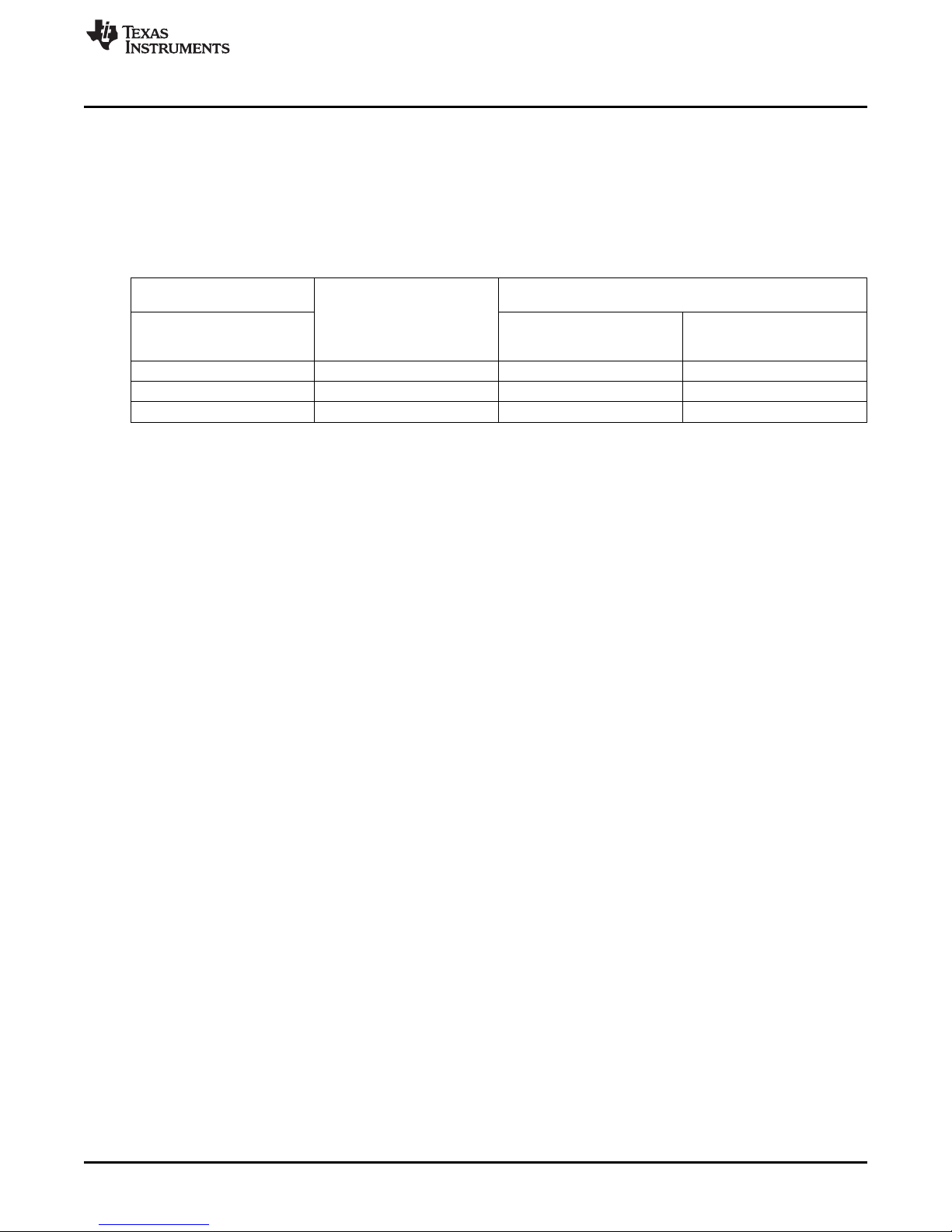
Features: Applications:
• Digital input mono speaker amp • Portable Audio Devices
• Supports 8-kHz to 96-kHz Sample Rates • White goods
• Mono Class-D BTL Speaker Driver (2.0 W Into • Portable Navigation Devices
4 Ω or 1.7 W Into 8 Ω)
• Mono Headphone/Lineout Driver
• Two Single-Ended Inputs With Output Mixing and
Level Control
• Embedded Power-on-Reset
• Integrated LDO
• Programmable Digital Audio Processing Blocks
for Bass Boost, Treble, EQ With up to Six
Biquads for Playback
• Integrated PLL Used for Programmable Digital
Audio Processing Blocks
• I2S, Left-Justified, Right-Justified, DSP, and TDM
Audio Interfaces
• I2C and SPI control with auto-increment
• Full Power-Down Control
• Power Supplies:
– Analog: 1.5 V–1.95 V
– Digital Core: 1.65 V–1.95 V
– Digital I/O: 1.1 V–3.6 V
– Class-D: 2.7 V–5.5 V (SPKVDD ≥ AVDD)
• 4mm × 4mm 24-Pin QFN Package
Chapter 1
SLAU472–February 2013
I2C is a trademark of NXP B.V. Corporation.
2
TAS2505 Device Overview SLAU472–February 2013
Copyright © 2013, Texas Instruments Incorporated
Submit Documentation Feedback
Page 3
DIN
BCLK
WCLK
MCLK
SPKVSS
AVSS
SCL/SSZ
SDA/MOSI
DVSS
AINL
AINR
SPKP
SPKM
HPOUT
RST
MISO
SPI_SEL
SCLK
6
6
SPKVDD
AVDD
LDO_SEL
DAC Signal
Proc.
Data
Interface
SPI/I2C
Control Block
PLL
Interrupt
Control
Primary I2S
Interface
Pin Muxing / Clock Routing
LDO
POR
Supplies
Mono 6
'DAC
DVDD
IOVDD
Secondary I2S
Interface
Dig
Vol
6 dB to +24 dB
(6 dB steps)
-6 dB to +29 dB
and Mute
(1 dB steps)
0 dB to -78 dB
and Mute
(Min 0.5 dB steps)
0 dB to -78 dB
and Mute
(Min 0.5 dB steps)
0 dB to -78 dB and Mute
(Min 0.5 dB steps)
www.ti.com
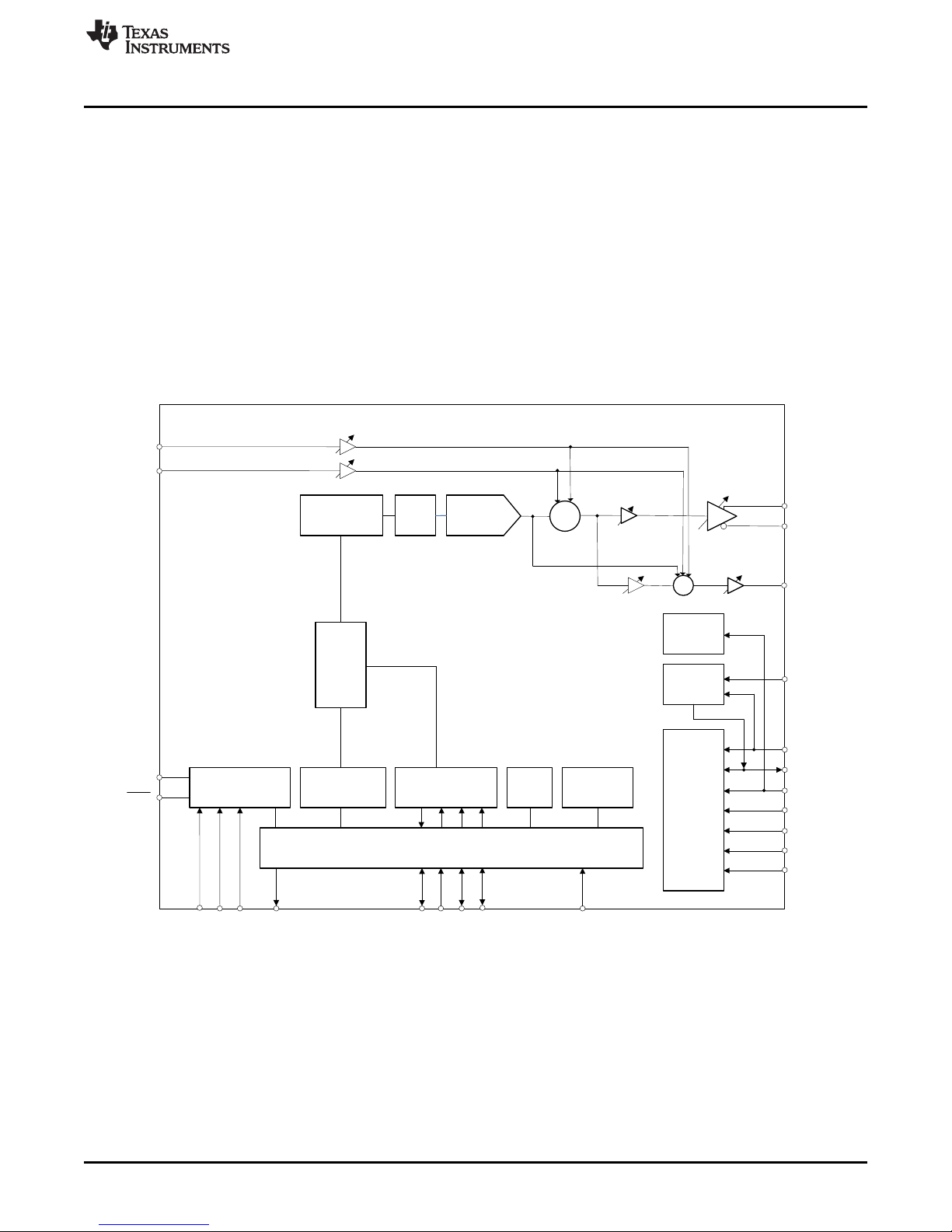
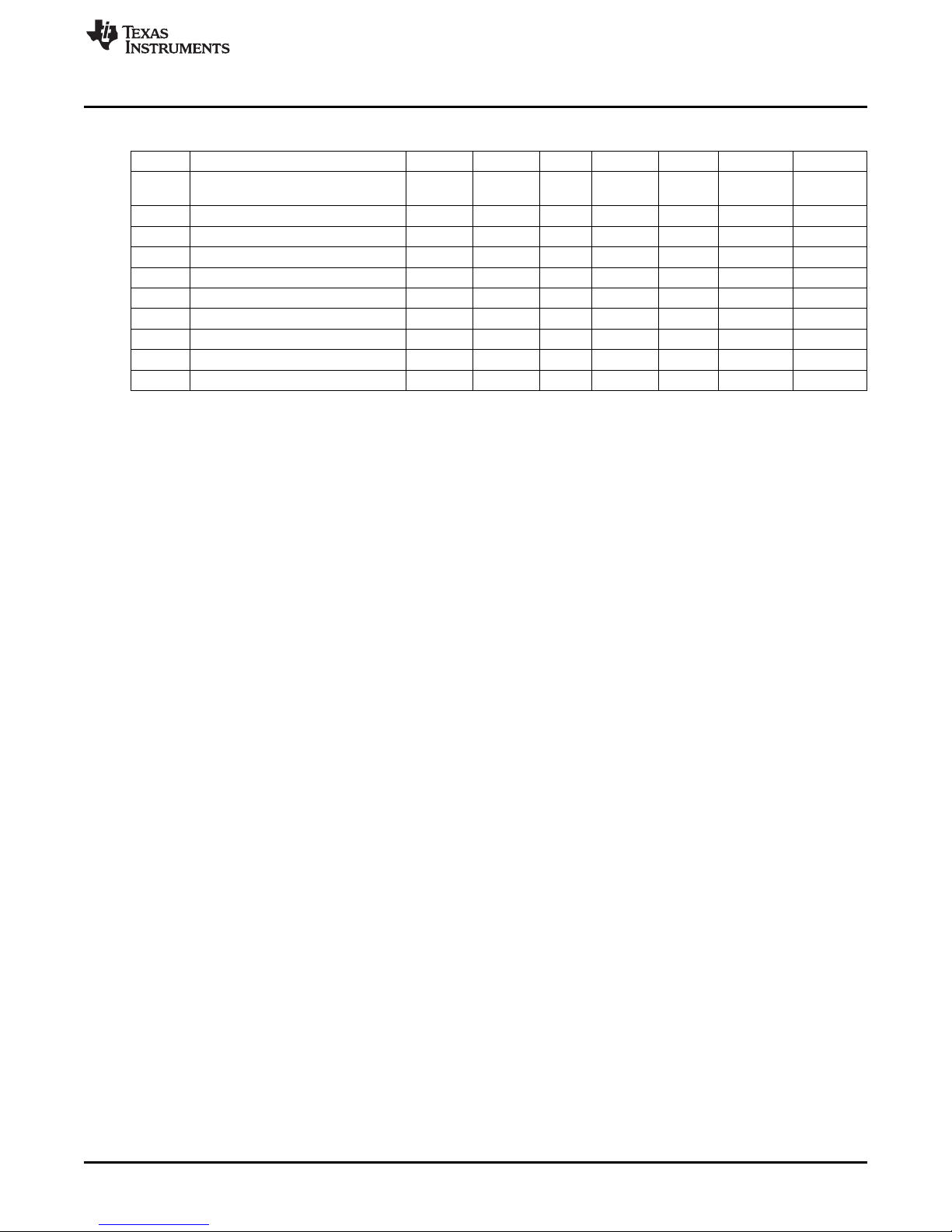
1.1 Description
The TAS2505 is a low power digital input speaker amp with support for 24-bit digital I2S data mono
playback.
In addition to driving a speaker amp upto 4-Ω, the device also features a mono headphone driver and a
programmable digital-signal processing block. The digital audio data format is programmable to work with
popular audio standard protocols (I2S, left/right-justified) in master, slave, DSP and TDM modes. The
programmable digital-signal processing block can support Bass boost, treble, or EQ functions. An on-chip
PLL provides the high-speed clock needed by the digital signal-processing block. The volume level can be
controlled by register control. The audio functions are controlled using the I2C™ serial bus or SPI bus. The
device includes an on-board LDO that runs off the speaker power supply to handle all internal device
analog and digital power needs. The included POR as power-on-resetcircuit reliably resets the device into
its default state so no external reset is required at normal usage; however, the device does have a reset
pin for more complex system initialization needs. The device also includes two analog inputs for mixing
and muxing in both speaker and headphone analog paths.
Description
Figure 1-1. Simplified Block Diagram
The device can cover operations from 8kHz mono playback to mono 96kHz DAC playback, making it ideal
for portable battery-powered audio and telephony applications. The playback path offers signal processing
blocks for filtering and effects, flexible mixing of analog input signals as well as programmable volume
controls. The voltage supply range for theTAS2505 for analog is 1.5V–1.95V, and for digital it is
1.65V–1.95V. To ease system-level design, a low-dropout regulator (LDO) is integrated to generate the
appropriate analog supply from input voltages ranging from 2.7V to 5.5V. Digital I/O voltages are
supported in the range of 1.1V–3.6V. The required internal clock of the TAS2505 can be derived from
SLAU472–February 2013 TAS2505 Device Overview
Submit Documentation Feedback
Copyright © 2013, Texas Instruments Incorporated
3
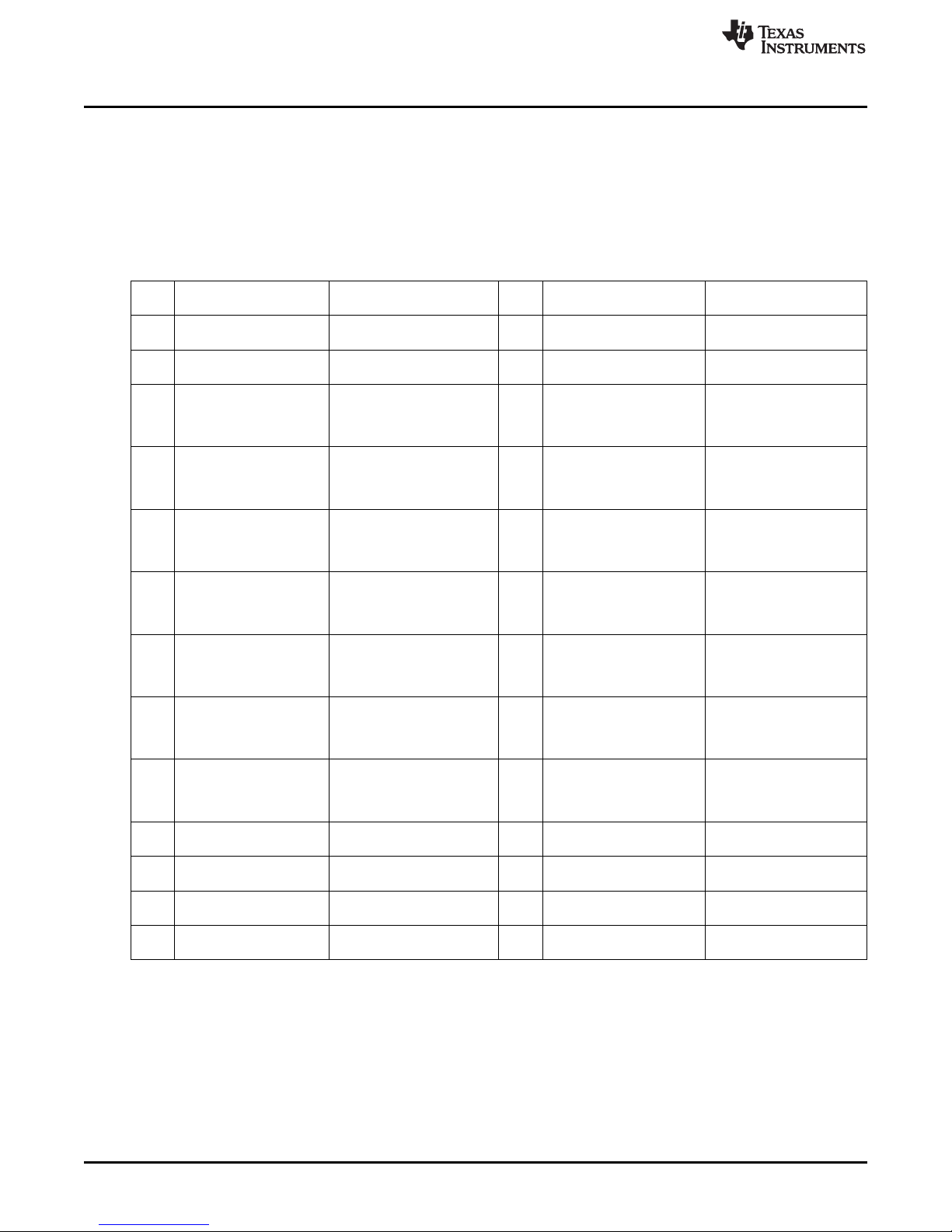
Page 4
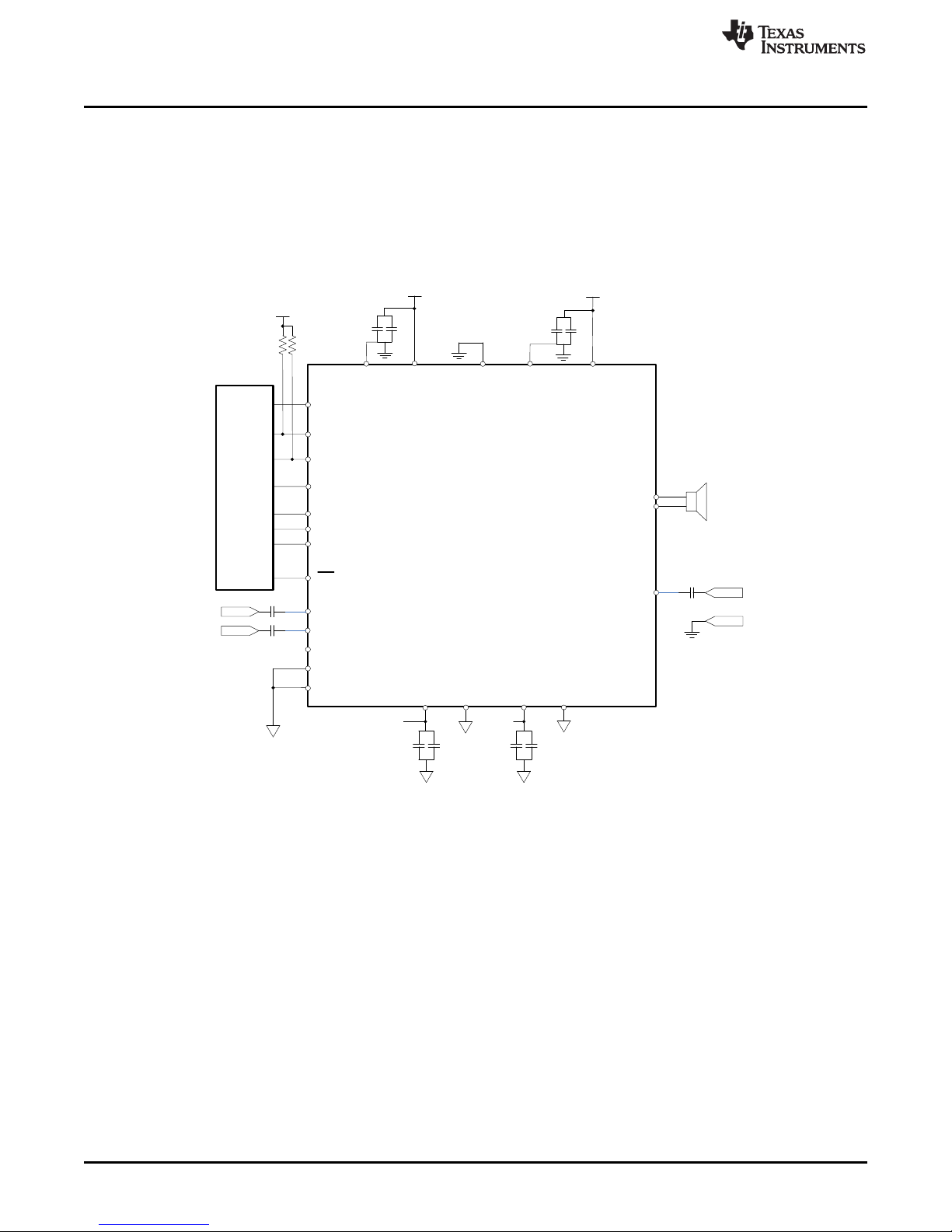
DIN
BCLK
WCLK
MCLK
SPKVSS
AVDDAVSS
LDO_SEL
SPKVDD
SCL/SSZ
SDA/MOSI
GPIO/DOUT
RST
DVDD DVSS IOVDD IOVSS
AINL
SPKP
SPKM
HOST PROCESSOR
0.1PF
22PF
SVDD
0.1PF
22PF
+1.8VA
8-: or
4-:
Speaker
+1.8VD IOVDD
AINR
Analog Input
TAS2505
HPOUT
Headphone jack
MISO
SPI_SEL
SCLK
IOVDD
0.1PF
0.1PF
2.7k
2.7k
47PF
0.1PF 0.1PF10PF
10PF
Typical Circuit Configuration
multiple sources, including the MCLK, BCLK or GPIO/DOUT pins or the output of the internal PLL, where
the input to the PLL again can be derived from the MCLK, BCLK or GPIO/DOUT pins. Although using the
internal, fractional PLL ensures the availability of a suitable clock signal, it is not recommended for the
lowest power settings. The PLL is highly programmable and can accept available input clocks in the range
of 512kHz to 50MHz.
The device is available in the 4mm × 4mm, 24-pin QFN package.
1.2 Typical Circuit Configuration
www.ti.com
4
TAS2505 Device Overview SLAU472–February 2013
Figure 1-2. Typical Circuit Configuration
Copyright © 2013, Texas Instruments Incorporated
Submit Documentation Feedback
Page 5
DIN
BCLK
WCLK
MCLK
SPKVSS
AVDDAVSS
LDO_SEL
SPKVDD
SCL/SSZ
SDA/MOSI
GPIO/DOUT
RST
IOVDD IOVSS
AINL
SPKP
SPKM
HOST PROCESSOR
0.1PF
22PF
SVDD
0.1PF
22PF
8-: or
4-:
Speaker
IOVDD
AINR
Analog Input
TAS2505
HPOUT
Headphone jack
MISO
SPI_SEL
SCLK
IOVDD
0.1PF
0.1PF
2.7k
2.7k
47PF
DVDDDVSS
0.1PF
10PF
0.1PF 10PF
www.ti.com
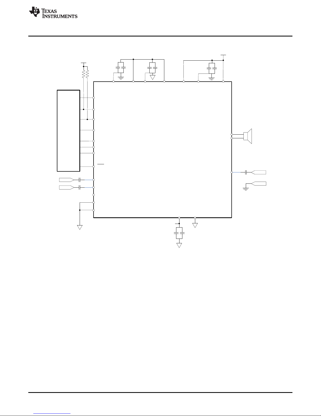
1.3 Circuit Configuration with Internal LDO
Circuit Configuration with Internal LDO
Figure 1-3. Application Schematics for LDO
SLAU472–February 2013 TAS2505 Device Overview
Submit Documentation Feedback
Copyright © 2013, Texas Instruments Incorporated
5
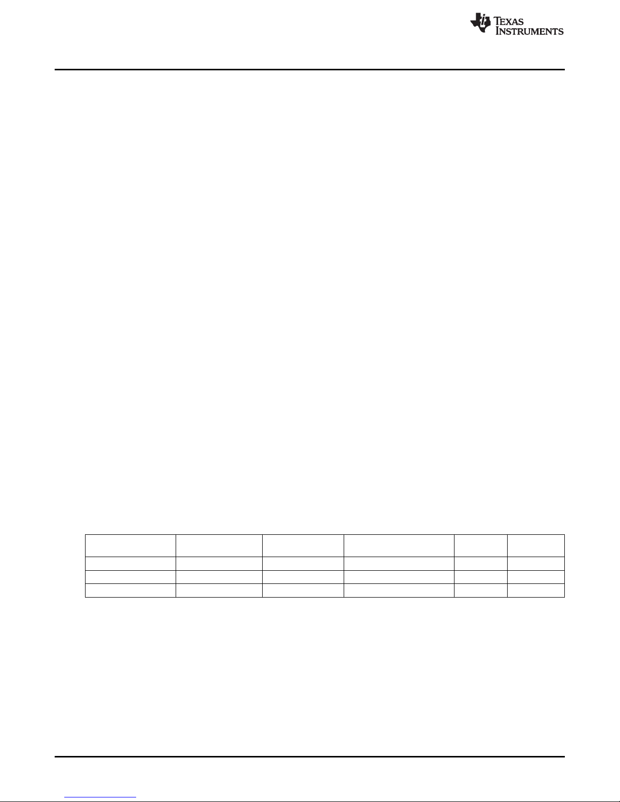
Page 6
2.1 Terminal Descriptions
2.1.1 Digital Pins
Only a small number of digital pins are dedicated to a single function; whenever possible, the digital pins
have a default function, and also can be reprogrammed to cover alternative functions for various
applications.
The fixed-function pins are RST LDO_SEL and the SPI_SEL pin, which are HW control pins. Depending
on the state of SPI_SEL, the two control-bus pins SCL/SSZ and SDA/MOSI are configured for either I2C or
SPI protocol.
Other digital IO pins can be configured for various functions via register control. An overview of available
functionality is given in Section 2.1.3.
2.1.2 Analog Pins
Analog functions can also be configured to a large degree. For minimum power consumption, analog
blocks are powered down by default. The blocks can be powered up with fine granularity according to the
application needs.
Chapter 2
SLAU472–February 2013
TAS2505 Application
2.1.3 Multifunction Pins
Table 2-1 shows the possible allocation of pins for specific functions. The PLL input, for example, can be
programmed to be any of 4 pins (MCLK, BCLK, DIN, GPIO).
Pin Function MCLK BCLK WCLK DIN GPIO SCLK MISO
A PLL Input S
B Codec Clock Input S
C I2S BCLK input S
D I2S BCLK output E
E I2S WCLK input E, D
F I2S WCLK output E
G I2S DIN E, D
I General Purpose Output I E
I General Purpose Output II E
J General Purpose Input I E
J General Purpose Input II E
J General Purpose Input III E
(1)S(1)
: The MCLK pin can drive the PLL and Codec Clock inputs simultaneously.
(2)S(2)
: The BCLK pin can drive the PLL and Codec Clock and audio interface bit clock inputs simultaneously.
(3)S(3)
: The GPIO/DOUT pin can drive the PLL and Codec Clock inputs simultaneously.
(4)
D: Default Function
(5)
E: The pin is exclusively used for this function, no other function can be implemented with the same pin. (If GPIO/DOUT has
been allocated for General Purpose Output, it cannot be used as the INT1 output at the same time.)
Table 2-1. Multifunction Pin Assignments
1 2 3 4 5 6 7
(1)
(1),D(4)
(2)
S
(2)
S
(2)
,D
(5)
E S
/DOUT
(3)
(3)
S
6
TAS2505 Application SLAU472–February 2013
Submit Documentation Feedback
Copyright © 2013, Texas Instruments Incorporated
Page 7
www.ti.com
Terminal Descriptions
Table 2-1. Multifunction Pin Assignments (continued)
1 2 3 4 5 6 7
Pin Function MCLK BCLK WCLK DIN GPIO SCLK MISO
/DOUT
K INT1 output E E
L INT2 output E E
M Secondary I2S BCLK input E E
N Secondary I2S WCLK input E E
O Secondary I2S DIN E E
P Secondary I2S BCLK OUT E E
Q Secondary I2S WCLK OUT E E
R Secondary I2S DOUT E
S Aux Clock Output E E
SLAU472–February 2013 TAS2505 Application
Submit Documentation Feedback
7
Copyright © 2013, Texas Instruments Incorporated
Page 8
Terminal Descriptions
2.1.4 Register Settings for Multifunction Pins
To configure the settings seen in Table 2-1, please see the letter-number combination in Table 2-2 for the
appropriate registers to modify. In Table 2-2, the letter/number combination represents the row and the
column number from Table 2-1 in bold type.
Please be aware that more settings may be necessary to obtain a full interface definition matching the
application requirement (see Page 0, Register 25 to 33).
Table 2-2. Multifunction Pin Register Configuration
Description Required Register Setting Description
A1 PLL Input on MCLK K7 INT1 output on MISO
A2 PLL Input on BCLK L5 INT2 output GPIO/DOUT
A4 PLL Input on DIN/MFP1 L7 INT2 output on MISO
A5 PLL Input on GPIO/DOUT M5
Codec Clock Input on Page 0, Register 4, Bits D1- Secondary I2S BCLK input D2-D1 = 01
B1 M6
MCLK D0 = 00 on SCLK Page 0, Register 31, Bits
Codec Clock Input on Page 0, Register 4, Bits D1- Secondary I2S WCLK in on D5-D2 = 0001
B2 N5
BCLK D0 = 01 GPIO/DOUT Page 0, Register 31, Bits
Codec Clock Input on D5-D2 = 0001 Secondary I2S WCLK in on D2-D1 = 01
B5 N6
GPIO/DOUT Page 0, Register 4, Bits D1- SCLK Page 0, Register 31, Bits
C2 I2S BCLK input on BCLK O5
D2 I2S BCLK output on BCLK O6
E3 I2S WCLK input on WCLK P5
F3 I2S WCLK output WCLK P7
G4 I2S DIN on DIN Q5
H5 N/A Q7
Page 0, Register 4, Bits D3- Page 0, Register 55, Bits
D2 = 00 D4-D1 = 0100
Page 0, Register 4, Bits D3- Page 0, Register 52, Bits
D2 = 01 D5-D2 = 0110
Page 0, Register 54, Bits
D2-D1 = 01 Page 0, Register 55, Bits
Page 0, Register 4, Bits D3- D4-D1 = 0101
D2 = 11
Page 0, Register 52, Bits Page 0, Register 52, Bits
D5-D2 = 0001 Secondary I2S BCLK input D5-D2 = 0001
Page 0, Register 4, Bits D3- on GPIO/DOUT Page 0, Register 31, Bits
D2 = 10 D6-D5 = 00
Page 0, Register 52, Bits Page 0, Register 56, Bits
D0 = 10 D4-D3 = 01
Page 0, Register 27, Bit D3 Secondary I2S DIN on D5-D2 = 0001
= 0 GPIO/DOUT Page 0, Register 31, Bit D0
Page 0, Register 27, Bit D3 Secondary I2S DIN on D2-D1 = 01
= 1 SCLK Page 0, Register 31, Bit D0
Page 0, Register 27, Bit D2 Secondary I2S BCLK OUT Page 0, Register 52, Bits
= 0 on GPIO/DOUT D5-D2 = 1000
Page 0, Register 27, Bit D2 Secondary I2S BCLK OUT Page 0, Register 55, Bits
= 1 on MISO D4-D1 = 1001
Page 0, Register 54, Bits Secondary I2S WCLK OUT Page 0, Register 52, Bits
D2-D1 = 01 on GPIO/DOUT D5-D2 = 1001
www.ti.com
Required Register
Setting
Page 0, Register 56, Bits
D6-D5 = 01
Page 0, Register 52, Bits
D4-D3 = 00
Page 0, Register 52, Bits
= 0
Page 0, Register 56, Bits
= 1
Secondary I2S WCLK OUT Page 0, Register 55, Bits
on MISO D4-D1 = 1010
8
TAS2505 Application SLAU472–February 2013
Submit Documentation Feedback
Copyright © 2013, Texas Instruments Incorporated
Page 9
www.ti.com
Description Required Register Setting Description
General Purpose Out I on Page 0, Register 53, Bits Secondary I2S DOUT on Page 0, Register 55, Bits
I5 R7
GPIO/DOUT D3-D1 = 010 MISO D4-D1 = 1000
General Purpose Out II Page 0, Register 55, Bits Aux Clock Output on Page 0, Register 52, Bits
I7 S5
on MISO D4-D1 = 0010 GPIO/DOUT D5-D2 = 0100
General Purpose In I on Page 0, Register 54, Bits Page 0, Register 55, Bits
J4 S7 Aux Clock Output on MISO
DIN D2-D1 = 10 D4-D1 = 0011
General Purpose In II on Page 0, Register 52, Bits
J5
GPIO/DOUT D5-D2 = 0010
General Purpose In III on Page 0, Register 56, Bits
J6
SCLK D2-D1 = 10
INT1 output on Page 0, Register 52, Bits
K5
GPIO/DOUT D5-D2 = 0101
2.2 Audio Analog I/O
The TAS2505 features a mono audio DAC. It supports a wide range of analog interfaces to support
different headsets such as 16-Ω to 200-Ω impedance and analog line outputs. TheTAS2505 can drive a
speaker upto 4-Ω impedance.
2.3 Analog Signals
Audio Analog I/O
Table 2-2. Multifunction Pin Register Configuration (continued)
Required Register
Setting
The TAS2505 analog signals consist of:
• Analog inputs AINR and AINL, which can be used to pass-through or mix analog signals to output
stages
• Analog outputs class-D speaker driver and headphone/lineout driver providing output capability for the
DAC, AINR, AINL, or a mix of the three
2.3.1 Analog Inputs AINL and AINR
AINL (pin 3 or C2) and AINR (pin 4 or B2) are inputs to Mixer P and Mixer M along with the DAC output.
Also AINL and AINR can be configured inputs to HP driver. Page1 / register 12 provides control signals for
determining the signals routed through Mixer P, Mixer M and HP driver. Input of Mixer P can be
attenuated by Page1 / register 24, input of Mixer M can be attenuated by Page1 / register 25 and input of
HP driver can be attenuated by Page1 / register 22. Also AINL and AINR can be configured to a monaural
differential input with use Mixer P and Mixer M by Page1 / register 12 setting. All the options can be
viewed in the functional block diagram, Figure 2-6.
2.4 Audio DAC and Audio Analog Outputs
The mono audio DAC consists of a digital audio processing block, a digital interpolation filter, a digital
delta-sigma modulator, and an analog reconstruction filter. The high oversampling ratio (normally DOSR is
between 32 and 128) exhibits good dynamic range by ensuring that the quantization noise generated
within the delta-sigma modulator stays outside of the audio frequency band. Audio analog outputs include
mono headphone and lineout and mono class-D speaker outputs. Because the TAS2505 contains a mono
DAC, it inputs the mono data from the left channel, the right channel, or a mix of the left and right
channels as [(L + R) ÷ 2], selected by page 0, register 63, bits D5–D4. See Figure 1-1 for the signal flow.
2.4.1 DAC
The TAS2505 mono audio DAC supports data rates from 8 kHz to 192 kHz. The audio channel of the
mono DAC consists of a signal-processing engine with fixed processing blocks, a digital interpolation filter,
multibit digital delta-sigma modulator, and an analog reconstruction filter. The DAC is designed to provide
enhanced performance at low sampling rates through increased oversampling and image filtering, thereby
keeping quantization noise generated within the delta-sigma modulator and observed in the signal images
SLAU472–February 2013 TAS2505 Application
Submit Documentation Feedback
9
Copyright © 2013, Texas Instruments Incorporated
Page 10
Audio DAC and Audio Analog Outputs
strongly suppressed within the audio band to beyond 20 kHz. To handle multiple input rates and optimize
power dissipation and performance, the TAS2505 allows the system designer to program the
oversampling rates over a wide range from 1 to 1024 by configuring page 0, register 13 and page 0 /
register 14. The system designer can choose higher oversampling ratios for lower input data rates and
lower oversampling ratios for higher input data rates.
The TAS2505 DAC channel includes a built-in digital interpolation filter to generate oversampled data for
the delta-sigma modulator. The interpolation filter can be chosen from three different types, depending on
required frequency response, group delay, and sampling rate.
DAC power up is controlled by writing to page 0, register 63, bit D7 for the mono channel. The monochannel DAC clipping flag is provided as a read-only bit on page 0 / register 39, bit D7.
The DAC path of the TAS2505 features many options for signal conditioning and signal routing:
• Digital volume control with a range of -63.5 to +24dB
• Mute function
In addition to the standard set of DAC features the TAS2505 also offers the following special features:
• Digital auto mute
• Adaptive filter mode
2.4.1.1 DAC Processing Blocks
The TAS2505 implements signal-processing capabilities and interpolation filtering via processing blocks.
These fixed processing blocks give users the choice of how much and what type of signal processing they
may use and which interpolation filter is applied.
The choices among these processing blocks allows the system designer to balance power conservation
and signal-processing flexibility. Table 2-3 gives an overview of all available processing blocks of the DAC
channel and their properties. The resource-class column gives an approximate indication of power
consumption for the digital (DVDD) supply; however, based on the out-of-band noise spectrum, the analog
power consumption of the drivers (AVDD) may differ.
The signal-processing blocks available are:
• First-order IIR
• Scalable number of biquad filters
The processing blocks are tuned for common cases and can achieve high image rejection or low group
delay in combination with various signal-processing effects such as audio effects and frequency shaping.
The available first-order IIR and biquad filters have fully user-programmable coefficients.
www.ti.com
Table 2-3. Overview – DAC Predefined Processing Blocks
Processing First-Order Number of Resource
Block No. IIR Available Biquads Class
PRB_P1 A Mono Yes 6 6
PRB_P2 A Mono No 3 4
PRB_P3 B Mono Yes 6 4
10
TAS2505 Application SLAU472–February 2013
Interpolation Filter Channel
Copyright © 2013, Texas Instruments Incorporated
Submit Documentation Feedback
Page 11
Interp.
Filter
A,B
BiQuad
F
BiQuad
E
BiQuad
D
BiQuad
C
BiQuad
B
BiQuad
A
IIR
to
Modulator
Digital
Volume
Ctrl
from
Interface
´
Interp.
Filter A
BiQuad
C
BiQuad
B
BiQuad
A
to
Modulator
Digital
Volume
Ctrl
from
Interface
´
www.ti.com
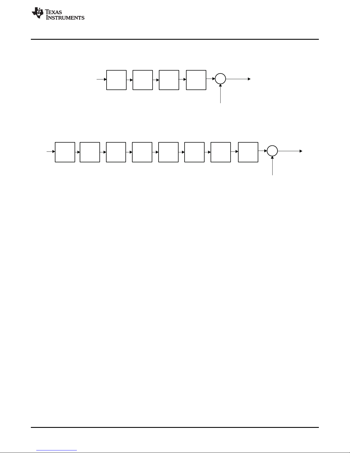
2.4.1.2 DAC Processing Blocks – Signal Chain Details
2.4.1.2.1 Three Biquads, Filter A
Figure 2-1. Signal Chain for PRB_P2
2.4.1.2.2 Six Biquads, First-Order IIR, Filter A or B
Figure 2-2. Signal Chain for PRB_P1 and PRB_P3
Audio DAC and Audio Analog Outputs
2.4.1.3 DAC User-Programmable Filters
Depending on the selected processing block, different types and orders of digital filtering are available. Up
to six biquad sections are available for specific processing blocks.
The coefficients of the available filters are arranged as sequentially-indexed coefficients in two banks. If
adaptive filtering is chosen, the coefficient banks can be switched in real time.
When the DAC is running, the user-programmable filter coefficients are locked and cannot be accessed
for either read or write.
However, the TAS2505 offers an adaptive filter mode as well. Setting page 8, register 1, bit D2 = 1 turns
on double buffering of the coefficients. In this mode, filter coefficients can be updated through the host and
activated without stopping and restarting the DAC. This enables advanced adaptive filtering applications.
In the double-buffering scheme, all coefficients are stored in two buffers (buffers A and B). When the DAC
is running and adaptive filtering mode is turned on, setting page 44, register 1, bit D0 = 1 switches the
coefficient buffers at the next start of a sampling period. This bit is set back to 0 after the switch occurs. At
the same time, page 44, register 1, bit D1 toggles.
The flag in page 44, register 1, bit D1 indicates which of the two buffers is actually in use.
Page 44, register 1, bit D1 = 0: buffer A is in use by the DAC engine; bit D1 = 1: buffer B is in use.
While the device is running, coefficient updates are always made to the buffer not in use by the DAC,
regardless of the buffer to which the coefficients have been written.
SLAU472–February 2013 TAS2505 Application
Submit Documentation Feedback
Copyright © 2013, Texas Instruments Incorporated
11
Page 12
-1 -2
0 1 2
23 -1 -2
1 2
N + 2 x N z + N z
H(z) =
2 - 2 x D z - D z
-
-
+
=
-
1
0 1
23 1
N N z
2 D z
Audio DAC and Audio Analog Outputs
Table 2-4. Adaptive-Mode Filter-Coefficient Buffer Switching
DAC Powered Coefficient Buffer in
Up Use
No 0 None C1, buffer A C1, buffer A
No 0 None C1, buffer B C1, buffer B
Yes 0 Buffer A C1, buffer A C1, buffer B
Yes 0 Buffer A C1, buffer B C1, buffer B
Yes 1 Buffer B C1, buffer A C1, buffer A
Yes 1 Buffer B C1, buffer B C1, buffer A
Page 44, Reg 1, Bit D1 I2C Writes to Will Updates
The user-programmable coefficients C1 to C70 for the DAC processing blocks are defined on pages 44 to
46 for buffer A and pages 62 to 64 for buffer B.
The coefficients of these filters are each 24-bit, 2s-complement format, occupying three consecutive 8-bit
registers in the register space. Specifically, the filter coefficients are in 1.23 (one dot 23) format with a
range from –1.0 (0x800000) to 0.99999988079071044921875 (0x7FFFFF) .
2.4.1.3.1 First-Order IIR Section
The IIR is of first order and its transfer function is given by
The frequency response for the first-order IIR section with default coefficients is flat.
www.ti.com
(1)
Filter Filter Coefficient Default (Reset) Values
First-order IIR N0 C65 (Page 46/ registers 28,29,30) 0x7FFFFF
2.4.1.3.2 Biquad Section
The transfer function of each of the biquad filters is given by
Filter Coefficient Mono DAC Channel Default (Reset) Values
Biquad A N0 C1 (Page 44, registers 12, 13, 14) 0x7FFFFF
Biquad B N0 C6( Page 44, registers 32, 33, 34) 0x7FFFFF
Table 2-5. DAC IIR Filter Coefficients
DAC Coefficient,
Mono Channel
N1 C66 (Page 46/ registers 32,33,34) 0x000000
D1 C67 (Page 46 / registers 36,37,38) 0x000000
(2)
Table 2-6. DAC Biquad Filter Coefficients
N1 C2 (Page 44, registers 16, 17, 18) 0x000000
N2 C3 (Page 44, registers 20, 21, 22) 0x000000
D1 C4 (Page 44, registers 24, 25, 26) 0x000000
D2 C5 (Page 44, registers 28, 29, 30) 0x000000
N1 C7 (Page 44, registers 36, 37, 38) 0x000000
N2 C8 (Page 44, registers 40, 41, 42) 0x000000
D1 C9 (Page 44, registers 44, 45, 46) 0x000000
D2 C10 (Page 44, registers 48, 49, 50) 0x000000
12
TAS2505 Application SLAU472–February 2013
Submit Documentation Feedback
Copyright © 2013, Texas Instruments Incorporated
Page 13
www.ti.com
Audio DAC and Audio Analog Outputs
Table 2-6. DAC Biquad Filter Coefficients (continued)
Filter Coefficient Mono DAC Channel Default (Reset) Values
Biquad C N0 C11 (Page 44, registers 52, 53, 54) 0x7FFFFF
N1 C12 (Page 44, registers 56, 57, 58) 0x000000
N2 C13 (Page 44, registers 60, 61, 62) 0x000000
D1 C14 (Page 44, registers 64, 65, 66) 0x000000
D2 C15 (Page 44, registers 68, 69, 70) 0x000000
Biquad D N0 C16 (Page 44, registers 72, 73, 74) 0x7FFFFF
N1 C17 (Page 44, registers 76, 77, 78) 0x000000
N2 C18 (Page 44, registers 80, 81, 82) 0x000000
D1 C19 (Page 44, registers 84, 85, 86) 0x000000
D2 C20 (Page 44, registers 88, 89, 90) 0x000000
Biquad E N0 C21 (Page 44, registers 92, 93, 94) 0x7FFFFF
N1 C22 (Page 44, registers 96, 97, 98) 0x000000
N2 C23 (Page 44, registers 100, 101, 102) 0x000000
D1 C24 (Page 44, registers 104, 105, 106) 0x000000
D2 C25 (Page 44, registers 108, 109, 110) 0x000000
Biquad F N0 C26 (Page 44, registers 112, 113, 114) 0x7FFFFF
N1 C27 (Page 44, registers 116, 117, 118) 0x000000
N2 C28 (Page 44, registers 120, 121, 122) 0x000000
D1 C29 (Page 44, registers 124, 125, 126) 0x000000
D2 C30 (Page 45, registers 8, 9, 10) 0x000000
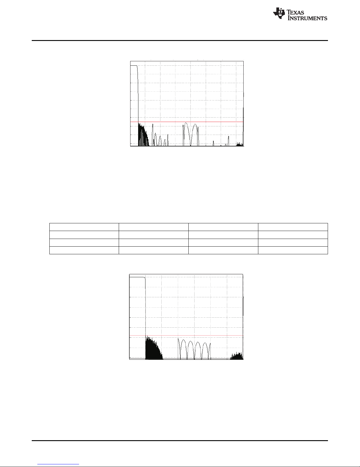
2.4.1.4 DAC Interpolation Filter Characteristics
2.4.1.4.1 Interpolation Filter A
Filter A is designed for an fSup to 48 ksps with a flat pass band of 0 kHz–20 kHz.
Table 2-7. Specification for DAC Interpolation Filter A
Parameter Condition Value (Typical) Unit
Filter-gain pass band 0 … 0.45 f
Filter-gain stop band 0.55 fS… 7.455 f
Filter group delay 21/f
S
S
±0.015 dB
–65 dB
S
s
SLAU472–February 2013 TAS2505 Application
Submit Documentation Feedback
13
Copyright © 2013, Texas Instruments Incorporated
Page 14
DACChannelResponseforInterpolationFilterB
(RedLineCorrespondsto –58dB)
0.5 1 1.5 2 2.5 3 3.5
FrequencyNormalizedtof
S
0
–10
–20
–30
–40
–50
–60
–70
–80
Magnitude – dB
0
–10
–20
–30
–40
–50
–60
–70
–80
–90
1
3 4
5 6
7
2
Magnitude – dB
FrequencyNormalizedtof
S
DACChannelResponseforInterpolationFilter A
(RedLineCorrespondsto –65dB)
Audio DAC and Audio Analog Outputs
Figure 2-3. Frequency Response of DAC Interpolation Filter A
2.4.1.4.2 Interpolation Filter B
Filter B is specifically designed for an fSup to 96 ksps. Thus, the flat pass-band region easily covers the
required audio band of 0 kHz–20 kHz.
www.ti.com
Table 2-8. Specification for DAC Interpolation Filter B
Parameter Condition Value (Typical) Unit
Filter-gain pass band 0 … 0.45 f
Filter-gain stop band 0.55 fS… 3.45 f
Filter group delay 18/f
14
TAS2505 Application SLAU472–February 2013
Figure 2-4. Frequency Response of Channel Interpolation Filter B
S
S
Copyright © 2013, Texas Instruments Incorporated
±0.015 dB
–58 dB
S
s
Submit Documentation Feedback
Page 15
www.ti.com
2.4.2 DAC Gain Setting
2.4.2.1 PowerTune Modes
As part of the PowerTune strategy, the analog properties of the DAC are adjusted. As a consequence, the
full-scale signal swing achieved at the headphone and line outputs must be adjusted. Please see Table 2-
9 for the proper gain compensation values across the different combinations.
Table 2-9. DAC Gain vs. PowerTune Modes
DAC PowerTune Mode PowerTune Mode Headphone Gain
Control
Page 1,Register 3, Bits (D4- CM = 0.75V, Gain for CM = 0.9V, Gain for
D2) 375mV
000 PTM_P3, PTM_P4 0 0
001 PTM_P2 4 4
010 PTM_P1 14 14
2.4.2.2 DAC Digital-Volume Control
The DAC has a digital volume-control block which implements programmable gain. Each channel has an
independent volume control that can be varied from 24 dB to –63.5 dB in 0.5-dB steps. The mono-channel
DAC volume can be controlled by writing to page 0, register 65, bits D7–D0. DAC muting and setting up a
master gain control to control the mono channel is done by writing to page 0, register 64, bits D3. The
gain is implemented with a soft-stepping algorithm, which only changes the actual volume by 0.125 dB per
input sample, either up or down, until the desired volume is reached. The rate of soft-stepping can be
slowed to one step per two input samples by writing to page 0, register 63, bits D1–D0. Note that the
default source for volume-control level settings is controlled by register writes to page 0, register 65.
During soft-stepping, the host does not receive a signal when the DAC has been completely muted. This
may be important if the host must mute the DAC before making a significant change, such as changing
sample rates. In order to help with this situation, the device provides a flag back to the host via a readonly register, page 0, register 38, bit D4 for the mono channel. This information alerts the host when the
part has completed the soft-stepping, and the actual volume has reached the desired volume level. The
soft-stepping feature can be disabled by writing to page 0, register 63, bits D1–D0.
If soft-stepping is enabled, the CODEC_CLKIN signal should be kept active until the DAC power-up flag is
cleared. When this flag is cleared, the internal DAC soft-stepping process is complete, and
CODEC_CLKIN can be stopped if desired. (The analog volume control can be ramped down using an
internal oscillator.)
Audio DAC and Audio Analog Outputs
output swing at 500mV
RMS
0dB full scale input 0dB full scale input
output swing at
RMS
2.4.3 Interrupts
Some specific events in the TAS2505, which may require host-processor intervention, can be used to
trigger interrupts to the host processor. This avoids polling the status-flag registers continuously. The
TAS2505 has two defined interrupts, INT1 and INT2, that can be configured by programming page 0,
register 48 and page 0, register 49. A user can configure interrupts INT1 and INT2 to be triggered by one
or many events, such as:
• Overcurrent condition in headphone drivers/speaker drivers
• Data overflow in the DAC processing blocks and filters
Each of these INT1 and INT2 interrupts can be routed to output pin GPIO. These interrupt signals can
either be configured as a single pulse or a series of pulses by programming page 0, register 48, bit D0
and page 0, register 49, bit D0. If the user configures the interrupts as a series of pulses, the events
trigger the start of pulses that stop when the flag registers in page 0, register 42 and page 0, register 44
are read by the user to determine the cause of the interrupt.
SLAU472–February 2013 TAS2505 Application
Submit Documentation Feedback
15
Copyright © 2013, Texas Instruments Incorporated
Page 16

Audio DAC and Audio Analog Outputs
2.4.4 Programming DAC Digital Filter Coefficients
The digital filter coefficients must be programmed through the control interface. All digital filtering for the
DAC signal path must be loaded into the RAM before the DAC is powered on. (Note that default
ALLPASS filter coefficients for programmable biquads are located in boot ROM. The boot ROM
automatically loads the default values into the RAM following a hardware reset (toggling the RST pin) or
after a software reset. After resetting the device, loading boot ROM coefficients into the digital filters
requires 100 μs of programming time. During this time, reading or writing to page 8 through page 15 for
updating DAC filter coefficient values is not permitted. (The DAC should not be powered up until after all
of the DAC configurations have been done by the system microprocessor.)
www.ti.com
16
TAS2505 Application SLAU472–February 2013
Copyright © 2013, Texas Instruments Incorporated
Submit Documentation Feedback
Page 17
Play- Paused
DACPowerDown
Update
DigitalFilter
Coefficients
DACPowerUP
Wait20ms
VolumeRampDown
SoftMute
Restore Previous
VolumeLevel(Ramp)
in(B)ms
Play- Continue
Wait(A)ms
Forf =32kHzS® Wait25ms(min)
Forf =48kHz Wait20ms(min)
S
®
For =32kHz ®f 25ms
Forf =48kHz 20ms
S
S
®
DACVolumeRampDownWAIT Time(A)
DACVolumeRampUp Time(B)
F0024-02
www.ti.com
2.4.5 Updating DAC Digital Filter Coefficients During PLAY
When it is required to update the DAC digital filter coefficients during play, care must be taken to avoid
click and pop noise or even a possible oscillation noise. These artifacts can occur if the DAC coefficients
are updated without following the proper update sequence. The correct sequence is shown in Figure 2-5.
The values for times listed in Figure 2-5 are conservative and should be used for software purposes.
There is also an adaptive mode, in which DAC coefficients can be updated while the DAC is on. For
details, see Section 2.4.1.3.
Audio DAC and Audio Analog Outputs
Figure 2-5. Example Flow For Updating DAC Digital Filter Coefficients During Play
SLAU472–February 2013 TAS2505 Application
Submit Documentation Feedback
17
Copyright © 2013, Texas Instruments Incorporated
Page 18

Audio DAC and Audio Analog Outputs
2.4.6 Digital Mixing and Routing
The TAS2505 has four digital mixing blocks. Each mixer can provide either mixing or multiplexing of the
digital audio data. The first mixer/multiplexer can be used to select input data for the mono DAC from left
channel, right channel, or (left channel + right channel) / 2 mixing. This digital routing can be configured by
writing to page 0, register 63, bits D5–D4.
2.4.7 Analog Audio Routing
The TAS2505 has the capability to route the DAC output to either the headphone or the speaker output. If
desirable, both output drivers can be operated at the same time while playing at different volume levels.
The TAS2505 provides various digital routing capabilities, allowing digital mixing or even channel
swapping in the digital domain. All analog outputs other than the selected ones can be powered down for
optimal power consumption.
2.4.7.1 Analog Output Volume Control
The output volume control can be used to fine-tune the level of the mixer amplifier signal supplied to the
headphone driver or the speaker driver. This architecture supports separate and concurrent volume levels
for each of the four output drivers. This volume control can also be used as part of the output pop-noise
reduction scheme. This feature is available even if the DAC is powered down.
2.4.7.2 Headphone Analog Output Volume Control
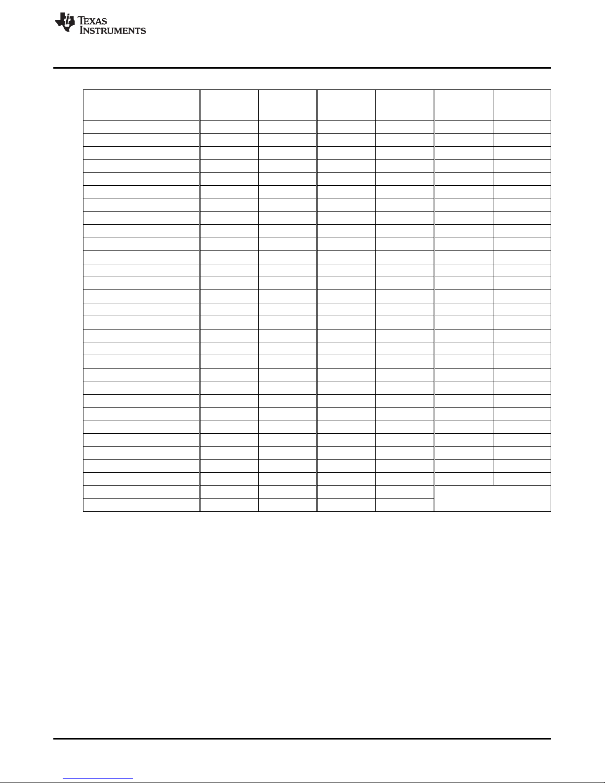
For the headphone output, the analog volume control has a range from 0 dB to –78 dB in 0.5-dB steps for
most of the useful range plus mute, as shown in Table 2-10. This volume control includes soft-stepping
logic.
Changing the analog volume for the headphone is controlled by writing to page 1, register 22, bits D6–D0.
Routing the signal from the output of the analog volume control to the input of the headphone power
amplifier via Mixer P and Mixer M is done by writing to page 1, register 12, bit D2.
The analog volume-control soft-stepping time is based on the setting in page 0, register 63, bits D1–D0.
www.ti.com
18
TAS2505 Application SLAU472–February 2013
Submit Documentation Feedback
Copyright © 2013, Texas Instruments Incorporated
Page 19
www.ti.com
Audio DAC and Audio Analog Outputs
Table 2-10. Analog Volume Control for Headphone and Speaker Outputs
Register Register Register Register
Value Value Value Value
0 0.0 30 –15.0 60 –30.1 90 –45.2
1 –0.5 31 –15.5 61 –30.6 91 –45.8
2 –1.0 32 –16.0 62 –31.1 92 –46.2
3 –1.5 33 –16.5 63 –31.6 93 –46.7
4 –2.0 34 –17.0 64 –32.1 94 –47.4
5 –2.5 35 –17.5 65 –32.6 95 –47.9
6 –3.0 36 –18.1 66 –33.1 96 –48.2
7 –3.5 37 –18.6 67 –33.6 97 –48.7
8 –4.0 38 –19.1 68 –34.1 98 –49.3
9 –4.5 39 –19.6 69 –34.6 99 –50.0
10 –5.0 40 –20.1 70 –35.2 100 –50.3
11 –5.5 41 –20.6 71 –35.7 101 –51.0
12 –6.0 42 –21.1 72 –36.2 102 –51.4
13 –6.5 43 –21.6 73 –36.7 103 –51.8
14 –7.0 44 –22.1 74 –37.2 104 –52.2
15 –7.5 45 –22.6 75 –37.7 105 –52.7
16 –8.0 46 –23.1 76 –38.2 106 –53.7
17 –8.5 47 –23.6 77 –38.7 107 –54.2
18 –9.0 48 –24.1 78 –39.2 108 –55.3
19 –9.5 49 –24.6 79 –39.7 109 –56.7
20 –10.0 50 –25.1 80 –40.2 110 –58.3
21 –10.5 51 –25.6 81 –40.7 111 –60.2
22 –11.0 52 –26.1 82 –41.2 112 –62.7
23 –11.5 53 –26.6 83 –41.7 113 –64.3
24 –12.0 54 –27.1 84 –42.1 114 –66.2
25 –12.5 55 –27.6 85 –42.7 115 –68.7
26 –13.0 56 –28.1 86 –43.2 116 –72.2
27 –13.5 57 –28.6 87 –43.8 117–127 –78.3
28 –14.0 58 –29.1 88 –44.3
29 –14.5 59 –29.6 89 –44.8
Analog Analog Analog Analog
Attenuation Attenuation Attenuation Attenuation
(dB) (dB) (dB) (dB)
2.4.7.3 Class-D Speaker Analog Output Volume Control
For the speaker outputs, the analog volume control has a range from 0 dB to –78 dB in 0.5-dB steps for
most of the useful range plus mute, as seen in Table 2-10. The implementation includes soft-stepping
logic.
Routing the DAC output signal to the analog volume control via Mixer P and Mixer M is done by writing to
page 1, register 12, bits D3. Changing the analog volume for the speaker is controlled by writing to page 1
/ register 46, bits D6–D0.
The analog volume-control soft-stepping time is based on the setting in page 0, register 63, bits D1–D0.
2.4.8 Analog Outputs
Various analog routings are supported for playback. All the options can be viewed in the functional block
diagram, Figure 2-6.
SLAU472–February 2013 TAS2505 Application
Submit Documentation Feedback
19
Copyright © 2013, Texas Instruments Incorporated
Page 20
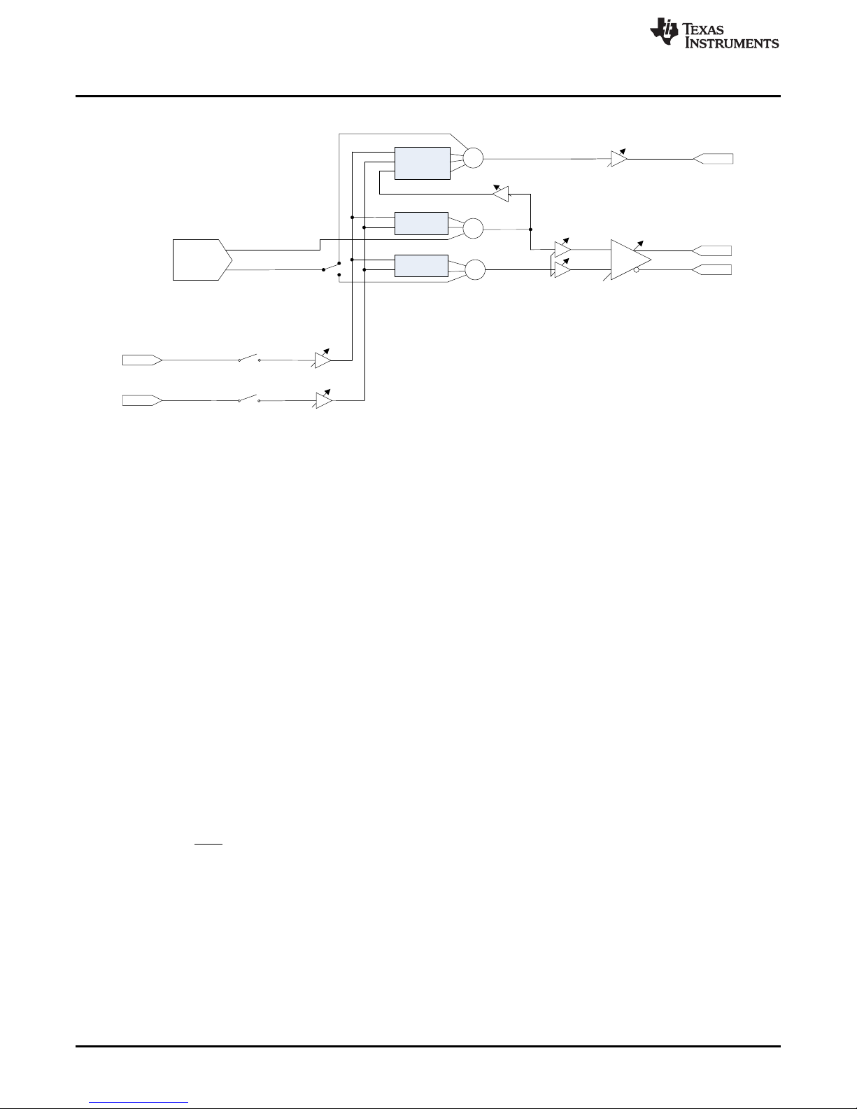
AINR
AINL
SPKP
SPKM
HPOUT
P1/R24
P1/R25
DAC
P1/R9/D1
P1/R48
P1/R16
Class-D Speaker
Driver
P1/R9/D0
DACP
DACM
P1/R46
Class A/B
Headphone Driver
Analog AttenuationAnalog Input Enable
Speaker Volume Control
Mixer M
Routing
Selection
6
6
6
HP Out Mixer
Note: If only use analog input from AINL or, and AINR to
HPOUT as P1/R12/D1=1 or, and P1/R12/D0=1, need to
set P1/R24/D7=1 as HP Out mixer forcedly powered-up.
Mixer P
P1/R12/D1
P1/R12/D0
P1/R12/D2
P1/R12/D7
P1/R12/D6
P1/R12/D5
P1/R12/D4
P1/R12/D3
P1/R22
HP Volume Control
Audio DAC and Audio Analog Outputs
2.4.8.1 Headphone Drivers
The TAS2505 features a mono headphone driver (HPOUT) that can deliver up to 28 mW channel, at 1.8-V
supply voltage, into a 16-Ω load. The headphones are used in a single-ended configuration where an accoupling (dc-blocking) capacitor is connected between the device output pins and the headphones. The
headphone driver also supports 32-Ω and 10-kΩ loads without changing any control register settings.
The headphone driver can be configured to reduce the power consumption in the half drive ability mode
by writing 1 to page 1, register 10, bits D2 = 1, also in this mode the headphone driver can support
lineout-drive as well.
The common-mode voltage is set to ≤ AVDD/2.
The headphone driver can be powered on by writing to page 1, register 9, bit D5. The HPOUT output
driver gain can be controlled by writing to page 1 / register 16 bits D5–D0, and it can be muted by writing
to page 1, register 16, bit D6.
The TAS2505 has a short-circuit protection feature for the headphone drivers, which is always enabled to
provide protection. The output condition of the headphone driver during short circuit can be programmed
by writing to page 1, register 11, bit D1. If D1 = 0 when a short circuit is detected, the device limits the
maximum current to the load. If D1 = 1 when a short circuit is detected, the device powers down the
output driver. The default condition for headphones is the current-limiting mode. For a short circuit on the
channel, the output is disabled and a status flag is provided as read-only bits on page 0 / register 45,
bit D5. If shutdown mode is enabled, then as soon as the short circuit is detected, page 0, register 9,
bit D5 (for HPOUT) clears automatically. Next, the device requires a reset to re-enable the output stage.
Resetting can be done in two ways. First, the device master reset can be used, which requires either
toggling the RST pin or using the software reset. If master reset is used, it resets all of the registers.
Second, a dedicated headphone power-stage reset can also be used to re-enable the output stage, and
that keeps all of the other device settings. The headphone power stage reset is done by setting page 1,
register 9, bit D5 for HPOUT. If the fault condition has been removed, then the device returns to normal
operation. If the fault is still present, then another shutdown occurs. Repeated resetting (more than three
times) is not recommended, as this could lead to overheating.
Figure 2-6. Analog Block Diagram
www.ti.com
20
TAS2505 Application SLAU472–February 2013
Copyright © 2013, Texas Instruments Incorporated
Submit Documentation Feedback
Page 21
www.ti.com
2.4.8.2 Speaker Driver
The TAS2505 has an integrated class-D mono speaker driver (SPKP/SPKM) capable of driving an 8-Ω or
4-Ω differential load. The speaker driver can be powered directly from the battery supply (2.7 V to 5.5 V)
on the SPKVDD pins; however, the voltage (including spike voltage) must be limited below the absolutemaximum voltage of 6 V.
The speaker driver is capable of supplying 800 mW per channel with a 3.6-V power supply. Through the
use of digital mixing, the device can connect one or both digital audio playback data channels to either
speaker driver; this also allows digital channel swapping if needed.
The class-D speaker driver can be powered on by writing to page 1, register 45, bit D1. The class-D
output-driver gain can be controlled by writing to page 1, register 48, bits D6–D4, and it can be muted by
writing to page 1, register 48, bit D6 - D4 = 000.
The TAS2505 has a short-circuit protection feature for the speaker drivers that is always enabled to
provide protection. If the output is shorted, the output stage shuts down on the overcurrent condition.
(Current limiting is not an available option for the higher-current speaker driver output stage.) In case of a
short circuit, the output is disabled and a status flag is provided as a read-only bit on page 0, register 46,
bit D7.
If shutdown occurs due to an overcurrent condition, then the device requires a reset to re-enable the
output stage. Resetting can be done in two ways. First, the device master reset can be used, which
requires either toggling the RST pin or using the software reset. If master reset is used, it resets all of the
registers. Second, a dedicated speaker power-stage reset can be used that keeps all of the other device
settings. The speaker power-stage reset is done by setting page 1, register 45, bit D1 for SPKP and
SPKM. If the fault condition has been removed, then the device returns to normal operation. If the fault is
still present, then another shutdown occurs. Repeated resetting (more than three times) is not
recommended, as this could lead to overheating.
To minimize battery current leakage, the SPKVDD voltage level should not be less than the AVDD
voltage level.
The TAS2505 has a thermal protection (OTP) feature for the speaker driver which is always enabled to
provide protection. If the device is overheated, then the output stops switching. When the device cools
down, the output resumes switching. An overtemperature status flag is provided as a read-only bit on
page 0, register 45, bit D7. The OTP feature is for self-protection of the device. If die temperature can be
controlled at the system/board level, then overtemperature does not occur.
Audio DAC and Audio Analog Outputs
2.4.9 Audio Output-Stage Power Configurations
After the device has been configured (following a RST) and the circuitry has been powered up, the audio
output stage can be powered up and powered down by register control.
These functions soft-start automatically. By using these register controls, it is possible to turn all four
stages on at the same time without turning two of them off.
See Table 2-11 for register control of audio output stage power configurations.
Table 2-11. Audio Output Stage Power Configurations
Audio Output Pins Desired Function Page 1 / Register, Bit Value
HPOUT Power-down HPOUT driver Page 1 / register 9, bit D5 = 0
HPOUT Power-up HPOUT driver Page 1 / register 8, bit D5 = 1
SPKP / SPKM Power-down class-D driver Page 1 / register 45, bit D1 = 0
SPKP / SPKM Power-up class-D driver Page 1 / register 45, bit D1 = 1
SLAU472–February 2013 TAS2505 Application
Submit Documentation Feedback
21
Copyright © 2013, Texas Instruments Incorporated
Page 22
Audio DAC and Audio Analog Outputs
2.4.10 5V LDO
The TAS2505 has a built-in LDO which can generate the analog supply (AVDD) also the digital supply
(DVDD) from input voltage range of 2.7 V to 5.5 V with high PSRR. If combined power supply current is
50 mA or less, then this LDO can deliver power to both analog and digital power supplies. If the only
speaker power supply is present and LDO Select pin is enabled, the LDO can power up without requiring
other supplies. This LDO requires a minimum dropout voltage of 300 mV and can support load currents up
to 50 mA. For stability reasons the LDO requires a minimum decoupling capacitor of 1 µF (±50%) on the
analog supply (AVDD) pin and the digital supply (DVDD) pin. If use this LDO output voltage for the digital
supply (DVDD) pin, the analog supply (AVDD) pin connected to the digital supply (DVDD) externally is
required.
The LDO is by default powered down for low sleep mode currents and can be enabled driving the
LDO_SEL pin to SPKVDD (Speaker power supply). When the LDO is disabled the AVDD pin is tri-stated
and the device AVDD needs to be powered using external supply. In that case the DVDD pin is also tristated and the device DVDD needs to be powered using external supply. The output voltage of this LDO
can be adjusted to a few different values as given in the Table 2-12. A Circuit Configuration with Internal
LDO is shown in Section 1.3
Page-1, Register 2, D(5:4) LDO Output
www.ti.com
Table 2-12. AVDD LDO Settings
00 1.8 V
01 1.6 V
10 1.7 V
11 1.5 V
22
TAS2505 Application SLAU472–February 2013
Copyright © 2013, Texas Instruments Incorporated
Submit Documentation Feedback
Page 23
Signal Processing
and Registers
POR
I2C I2S
I2C Watchdog
SW RSTB
DVDD
DVDD
DVDD
DVDDDVDD
/RST
IOVDD to DVDD
Translator
IOVDD
DVDD
DVDD
DIN BCLKWCLK
SCL/
SSZ
SDA/
MOSI
LDO_SEL
LDO
(Battery Input
2.7V– 5.5V)
SPKVDD
AVDDDVDDIOVDD
To
Analog
Section
To
Digital
Section
1) pin resets IRST
2 2
C, I S, Signal Processing and all registers.
2) POR_RTB resets I C, I S, Signal Processing and all registers.
2 2
3) SW_
registers but not digital interfaces
RSTB from register bit resets only the Signal Processing
and all
.
POR_RSTB
After
15
SCLs
1.8V
Default
IOVDD
DVDD
POR_RSTB
time
time
time
SCLK
www.ti.com
2.4.11 POR
TAS2505 has a POR (Power On Reset) function as shown Figure 2-7. This function insures that all
registers are automatically set to defaults when a proper power up sequence is executed. The function
consume approximately 35uA from the DVDD so if needed this can be disabled by page 1, register 1, bit
D3 = 1.
Audio DAC and Audio Analog Outputs
SLAU472–February 2013 TAS2505 Application
Submit Documentation Feedback
Figure 2-7. POR Diagram
Copyright © 2013, Texas Instruments Incorporated
23
Page 24

Audio DAC and Audio Analog Outputs
2.4.12 DAC Setup
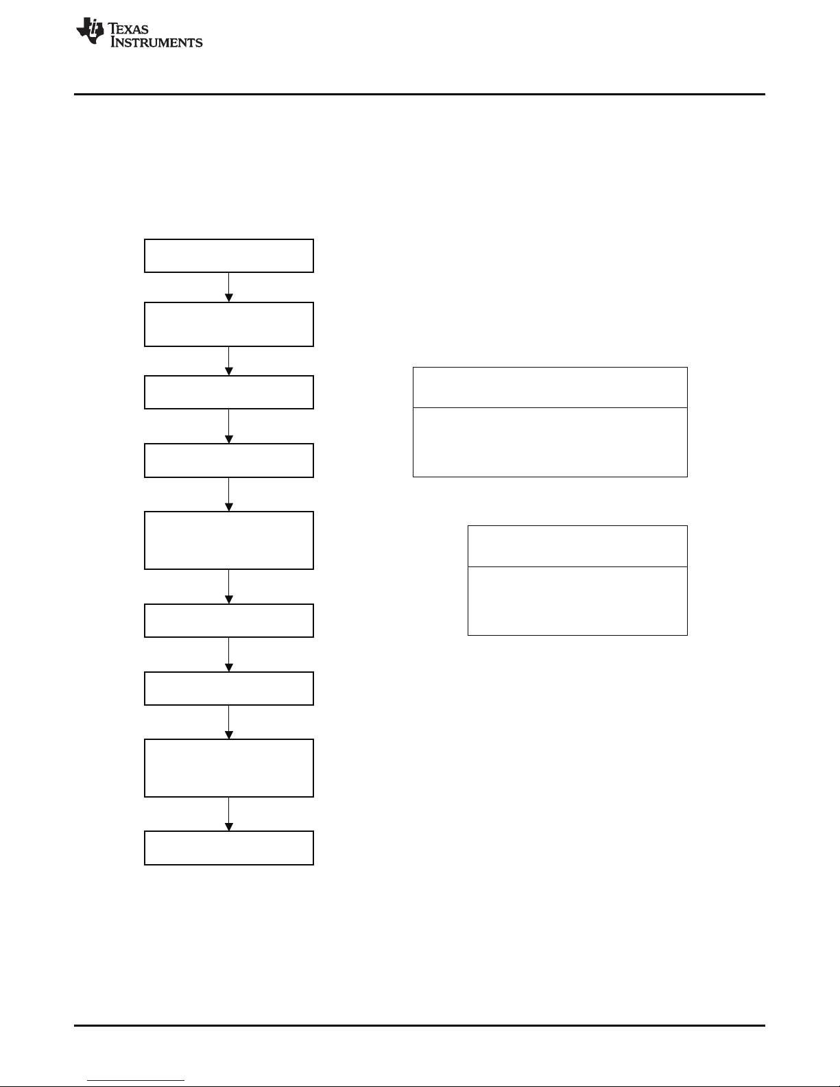
The following paragraphs are intended to guide a user through the steps necessary to configure the
TAS2505.
Step 1
The system clock source (master clock) and the targeted DAC sampling frequency must be identified.
Depending on the targeted performance, the decimation filter type (A or B) and DOSR value can be
determined:
• Filter A should be used for 48-kHz high-performance operation; DOSR must be a multiple of 8.
• Filter B should be used for up to 96-kHz operations; DOSR must be a multiple of 4.
In all cases, DOSR is limited in its range by the following condition:
2.8 MHz < DOSR x DAC_fS < 6.2 MHz (3)
Based on the identified filter type and the required signal processing capabilities, the appropriate
processing block can be determined from the list of available processing blocks (PRB_P1, PRB_P2 and
PRB_P3).
Based on the available master clock, the chosen DOSR and the targeted sampling rate, the clock divider
values NDAC and MDAC can be determined. If necessary, the internal PLL can add a large degree of
flexibility.
In summary, CODEC_CLKIN (derived directly from the system clock source or from the internal PLL)
divided by MDAC, NDAC, and DOSR must be equal to the DAC sampling rate DAC_fS. The
CODEC_CLKIN clock signal is shared with the DAC clock generation block.
CODEC_CLKIN = NDAC × MDAC × DOSR × DAC_fS (4)
NDAC and MDAC can be chosen independently in the range of 1 to 128. In general, NDAC should be as
large as possible as long as the following condition can still be met:
MDAC × DOSR / 32 ≥ RC (5)
RC is a function of the chosen processing block and is listed in Table 2-3.
The common-mode voltage setting of the device is determined by the available analog power supply. This
common-mode (input common-mode) value is common across the ADC, DAC and analog bypass path.
The output common-mode setting is determined by the available analog power supplies (AVdd and ) and
the desired output-signal swing.
At this point, the following device specific parameters are known:
PRB_Rx, DOSR, NDAC, MDAC, input and output common-mode values.
If the PLL is used, the PLL parameters P, J, D and R are determined as well.
Step 2
Setting up the device via register programming:
The following list gives a sequence of items that must be executed in the time between powering the
device up and reading data from the device:
1. Define starting point:
(a) Power up applicable external power supplies
(b) Set register page to 0
(c) Initiate SW reset
2. Program Clock Settings
(a) Program PLL clock dividers P, J, D and R (if PLL is necessary)
(b) Power up PLL (if PLL is necessary)
(c) Program and power up NDAC
(d) Program and power up MDAC
(e) Program OSR value
(f) Program I2S word length if required (16, 20, 24, or 32 bits)
(g) Program the processing block to be used
www.ti.com
24
TAS2505 Application SLAU472–February 2013
Copyright © 2013, Texas Instruments Incorporated
Submit Documentation Feedback
Page 25
www.ti.com
(h) Micellaneous page 0 controls
At this point, at the latest, the analog power supply must be applied to the device
3. Program Analog Blocks
(a) Set register page to 1
(b) Disable coarse AVDD generation
(c) Enable Master Analog Power Control
(d) Program common-mode voltage
(e) Program headphone-specific de-pop settings (if a headphone driver is used)
(f) Program routing of DAC output to the output amplifier (headphone and lineout or speaker)
(g) Unmute and set gain of output drivers
(h) Power up output drivers
4. Apply waiting time determined by the de-pop settings and the soft-stepping settings of the driver gain
or poll page 1, register 63
5. Power up DAC
(a) Set register page to 0
(b) Power up DAC channels and set digital gain
(c) Unmute digital volume control
Detailed examples can be found from Section 4.0.7 to Section 4.0.12.
2.5 PowerTune
PowerTune
The TAS2505features PowerTune, a mechanism to balance power-versus-performance tradeoffs at the
time of device configuration. The device can be tuned to minimize power dissipation, to maximize
performance, or to an operating point between the two extremes to best fit the application.
2.5.1 PowerTune Modes
2.5.1.1 DAC - Programming PTM_P1 to PTM_P4
On the playback side, the performance is determined by a combination of register settings and the audio
data word length applied. For the highest performance setting (PTM_P4), an audio-data word length of 20
bits is required, while for the modes PTM_P1 to PTM_P3 a word length of 16 bits is sufficient.
PTM_P1 PTM_P2 PTM_P3 PTM_P4
Pg 1, Reg 3, D(4:2) 0x2 0x1 0x0 0x0
Audio Data word length 16 bits 16 bits 16 bits 20 or more bits
Pg 0, Reg 27, D(5:4) 0x00 0x00 0x00 0x1, 0x2, 0x3
2.5.1.2 Processing Blocks
The choice of processing blocks, PRB_P1 to PRB_P3 for playback, also influences the power
consumption. In fact, the numerous processing blocks have been implemented to offer a choice between
power-optimization and configurations with more signal-processing resources.
SLAU472–February 2013 TAS2505 Application
Submit Documentation Feedback
25
Copyright © 2013, Texas Instruments Incorporated
Page 26
PowerTune
www.ti.com
2.5.2 DAC Power Consumption
The tables in this section give recommendations for various DAC PowerTune modes. Typical performance
and power-consumption numbers for line-out signals are listed.
All measurements were taken with the PLL turned off, no signal is present, and the DAC modulator is fully
running. PowerTune modes which are not supported are marked with an ‘X’.
2.5.2.1 DAC, Mono, 48 kHz, Highest Performance, DVDD = IOVDD = 1.8 V, AVDD = 1.8 V, SPKVDD = 3.6V
DOSR = 128, Processing Block = PRB_P3 (Interpolation Filter B)
Device Common Mode Setting = 0.75V Device Common Mode Setting = 0.9V
PTM_P1 PTM_P2 PTM_P3 PTM_P4 PTM_P1 PTM_P2 PTM_P3 PTM_P4 Unit
0dB full scale
HP out Idle Channle Noise 16.8 16.9 17.1 17.0 19.4 20.0 20.1 20.0 uV
(16-Ω
load)
(1)
Reduced 0dB full-scale swing can be compensated by applying appropriate gain in the output drivers see Section 2.4.2.1.
Power consumption 7.2 7.4 7.7 7.7 7.3 7.7 8.0 8.1 mW
Alternative Processing Blocks:
Processing Block Filter Estiamted Power Change at PTM_P3
PRB_P1 A +1.34 +1.30
PRB_P2 A -0.11 -0.11
(1)
75 225 375 375 100 300 500 500 mV
HP out
CM = 0.75V CM = 0.9V Unit
mW
RMS
2.5.2.2 DAC, Mono, Lowest Power Consumption
DOSR = 64, Processing Block = PRB_P3 (Interpolation Filter B)
0dB full scale
HP out
(16-Ω load)
(1)
Reduced 0dB full-scale swing can be compensated by applying appropriate gain in the output drivers see Section 2.4.2.1.
(1)
Idle Channle Noise 16.8 19.3 uV
Power consumption 5.8 6.7 mW
Alternative Processing Blocks:
Processing Block Filter Estiamted Power Change at PTM_P1
PRB_P1 A +1.46 +1.49
PRB_P2 A 0.00 +0.03
CM = 0.75V CM = 0.9V
AVDD = 1.5V AVDD = 1.8V
PTM_P1 PTM_P1
75 100 mV
HP out Unit
CM = 0.75V CM = 0.9V
Unit
RMS
mW
26
TAS2505 Application SLAU472–February 2013
Copyright © 2013, Texas Instruments Incorporated
Submit Documentation Feedback
Page 27
www.ti.com
PowerTune
2.5.2.3 DAC, Mono, 8 kHz, Highest Performance, DVDD = IOVDD = 1.8 V, AVDD = 1.8 V, SPKVDD = 3.6V
DOSR = 768, Processing Block = PRB_P2 (Interpolation Filter A)
Device Common Mode Setting = Device Common Mode Setting = 0.9V
0.75V
PTM_P1 PTM_P2 PTM_P3 PTM_P4 PTM_P1 PTM_P2 PTM_P3 PTM_P4 Unit
0dB full scale
HP out
(16-Ω load)
(1)
Reduced 0dB full-scale swing can be compensated by applying appropriate gain in the output drivers see Section 2.4.2.1.
(1)
75 225 375 375 100 300 500 500 mV
Idle Channle Noise 14.3 14.3 14.5 14.4 16.7 16.8 16.9 17.3 uV
Power 5.8 6.0 6.2 6.3 5.8 6.2 6.4 6.5 mW
consumption
Alternative Processing Blocks:
Processing Block Filter Estiamted Power Change at PTM_P1
PRB_P1 A +0.46 +0.53
PRB_P3 B +0.19 +0.26
2.5.2.4 DAC, Mono, Lowest Power Consumption
DOSR = 384, Processing Block = PRB_P2 (Interpolation Filter A)
0dB full scale
HP out
(16-Ω load)
(1)
Reduced 0dB full-scale swing can be compensated by applying appropriate gain in the output drivers see Section 2.4.2.1.
(1)
Idle Channle Noise 14.2 16.9 uV
Power consumption 4.2 5.1 mW
HP out Unit
CM = 0.75V CM = 0.9V
CM = 0.75V CM = 0.9V
AVDD = 1.5V AVDD = 1.8V
PTM_P1 PTM_P1
75 100 mV
RMS
mW
Unit
RMS
Alternative Processing Blocks:
Processing Block Filter Estiamted Power Change at PTM_P1
PRB_P1 A +0.43 +0.43
PRB_P3 B +0.17 +0.18
SLAU472–February 2013 TAS2505 Application
Submit Documentation Feedback
HP out Unit
CM = 0.75V CM = 0.9V
mW
27
Copyright © 2013, Texas Instruments Incorporated
Page 28

PowerTune
www.ti.com
2.5.3 Speaker output Power Consumption
To consider Speaker output power consumption on the TAS2505, the tables in this section to be may
useful to know the power consumption for each power rail. The tables shows selected as representable
combination of PRB mode and PTM mode.
All measurements were taken with the PLL turned off, no signal is present, and the DAC modulator is fully
running.
2.5.3.1 Speaker output, Mono, 48 kHz, Highest Performance, DVDD = IOVDD = 1.8 V, AVDD = 1.8 V,
SPKVDD = 3.6V
DOSR = 128, PRB mode = PRB_P3, PTM mode = PTM_P3, CM = 0.9V
iSVDD iAVDD iDVDD iIOVDD Total
SPK Driver Power consumption 28.51 3.26 3.71 0.01 35.5 mW
(4-Ω load)
2.5.3.2 Speaker output, Mono, Lowest Power Consumption
DOSR = 64, PRB mode = PRB_P3, PTM mode = PTM_P3, CM = 0.9V
iSVDD iAVDD iDVDD iIOVDD Total
SPK Driver Power consumption 28.50 3.26 3.01 0.01 34.8 mW
(4-Ω load)
2.5.3.3 Speaker output, Mono, 8 kHz, Highest Performance, DVDD = IOVDD = 1.8 V, AVDD = 1.8 V,
SPKVDD = 3.6V
DOSR = 768, PRB mode = PRB_P2, PTM mode = PTM_P3, CM = 0.9V
iSVDD iAVDD iDVDD iIOVDD Total
SPK Driver Power consumption 28.49 3.26 2.23 0.01 34.0 mW
(4-Ω load)
2.5.3.4 Speaker output, Mono, Lowest Power Consumption
DOSR = 384, PRB mode = PRB_P2, PTM mode = PTM_P3, CM = 0.9V
iSVDD iAVDD iDVDD iIOVDD Total
SPK Driver Power consumption 28.49 3.26 1.53 0.01 33.3 mW
(4-Ω load)
28
TAS2505 Application SLAU472–February 2013
Copyright © 2013, Texas Instruments Incorporated
Submit Documentation Feedback
Page 29

www.ti.com
PowerTune
2.5.4 Headphone output Power Consumption
To consider Headphone output power consumption on the TAS2505, the tables in this section to be may
useful to know the power consumption for each power rail. The tables shows selected as representable
combination of PRB mode and PTM mode.
All measurements were taken with the PLL turned off, no signal is present, and the DAC modulator is fully
running.
2.5.4.1 Headphone output, Mono, 48 kHz, Highest Performance, DVDD = IOVDD = 1.8 V, AVDD = 1.8 V,
SPKVDD = 3.6V
DOSR = 128, PRB mode = PRB_P3, PTM mode = PTM_P3, CM = 0.9V
iSVDD iAVDD iDVDD iIOVDD Total
Headphone Driver Power consumption 0.11 4.50 3.42 0.01 8.0 mW
(16-Ω load)
2.5.4.2 Headphone output, Mono, Lowest Power Consumption, DVDD = IOVDD = 1.8 V, AVDD = 1.5 V,
SPKVDD = 3.6V
DOSR = 64, PRB mode = PRB_P3, PTM mode = PTM_P1, CM = 0.75V
iSVDD iAVDD iDVDD iIOVDD Total
Headphone Driver Power consumption 0.12 2.97 2.68 0.01 5.8 mW
(16-Ω load)
2.5.4.3 Headphone output, Mono, 8 kHz, Highest Performance, DVDD = IOVDD = 1.8 V, AVDD = 1.8 V,
SPKVDD = 3.6V
DOSR = 768, PRB mode = PRB_P2, PTM mode = PTM_P3, CM = 0.9V
iSVDD iAVDD iDVDD iIOVDD Total
Headphone Driver Power consumption 0.13 4.43 1.82 0.01 6.4 mW
(16-Ω load)
2.5.4.4 Headphone output, Mono, Lowest Power Consumption, DVDD = IOVDD = 1.8 V, AVDD = 1.8 V,
SPKVDD = 3.6V
DOSR = 384, PRB mode = PRB_P2, PTM mode = PTM_P1, CM = 0.75V
iSVDD iAVDD iDVDD iIOVDD Total
Headphone Driver Power consumption 0.12 2.96 1.11 0.01 4.2 mW
(16-Ω load)
SLAU472–February 2013 TAS2505 Application
Submit Documentation Feedback
29
Copyright © 2013, Texas Instruments Incorporated
Page 30

PLL
´ ´(R J.D)/P
PLL_CLKIN
CODEC_CLKIN
DAC_MOD_CLK
DAC_CLK
NDAC = 1, 2, ..., 127, 128
MDAC = 1, 2, ..., 127, 128
DOSR = 1, 2, ..., 1023, 1024
MCLK
BCLK
GPIO
DIN
MCLK
BCLK
GPIO
PLL_CLK
¸MDAC
¸DOSR
¸NDAC
To DAC Digital Effects
DAC_f
S
CLOCK Generation and PLL
2.6 CLOCK Generation and PLL
The TAS2505 supports a wide range of options for generating clocks for the DAC sections as well as
interface and other control blocks as shown in . The clocks for the DAC require a source reference clock.
This clock can be provided on a variety of device pins, such as the MCLK, BCLK, or GPIO pins. The
source reference clock for the codec can be chosen by programming the CODEC_CLKIN value on page
0, register 4, bits D1–D0. The CODEC_CLKIN can then be routed through highly-flexible clock dividers
shown in to generate the various clocks required for the DAC and the Digital Effects section. In the event
that the desired audio clocks cannot be generated from the reference clocks on MCLK, BCLK, or GPIO,
the TAS2505 also provides the option of using the on-chip PLL which supports a wide range of fractional
multiplication values to generate the required clocks. Starting from CODEC_CLKIN, the TAS2505 provides
several programmable clock dividers to help achieve a variety of sampling rates for the DAC and clocks
for the Digital Effects sections.
www.ti.com
30
TAS2505 Application SLAU472–February 2013
Figure 2-8. Clock Distribution Tree
Copyright © 2013, Texas Instruments Incorporated
Submit Documentation Feedback
Page 31

÷N
BCLK
DAC_CLK DAC_MOD_CLK
BDIV_CLKIN
N = 1, 2, ..., 127, 128
B0362-01
S
CODEC _ CLKIN
NDAC MDAC DOSR
=
´ ´
CODEC _ CLKIN
NDAC MDAC
=
´
www.ti.com
The DAC modulator is clocked by DAC_MOD_CLK. For proper power-up operation of the DAC channel,
these clocks must be enabled by configuring the NDAC and MDAC clock dividers (page 0, register 11,
bit D7 = 1 and page 0, register 12, bit D7 = 1). When the DAC channel is powered down, the device
internally initiates a power-down sequence for proper shut-down. During this shutdown sequence, the
NDAC and MDAC dividers must not be powered down, or else a proper low-power shutdown may not take
place. The user can read back the power-status flag at page 0, register 37, bit D7 and page 0, register 37,
bit D3. When both the flags indicate power-down, the MDAC divider may be powered down, followed by
the NDAC divider.
In general, all the root clock dividers should be powered down only after the child clock dividers have been
powered down for proper operation.
The TAS2505 also has options for routing some of the internal clocks to the GPIO output pin to be used
as general-purpose clocks in the system. The feature is shown in Figure 2-10.
CLOCK Generation and PLL
(6)
Table 2-13. CODEC CLKIN Clock Dividers
Divider Bits
NDAC Page 0, register 11, bits D6–D0
MDAC Page 0, register 12, bits D6–D0
DOSR Page 0, register 13, bits D1–D0 and page 0, register 14, bits D7–D0
In the mode when TAS2505 is configured to drive the BCLK pin (page 0, register 27, bit D3 = 1), it can be
driven as a divided value of BDIV_CLKIN. The division value can be programmed in page 0, register 30,
bits D6–D0 from 1 to 128 (see Figure 2-9). The BDIV_CLKIN can itself be configured to be one of
DAC_CLK (DAC DSP clock) or DAC_MOD_CLK by configuring the BDIV_CLKIN multiplexer in page 0,
register 29, bits D1-D0. Additionally, a general-purpose clock can be driven out on GPIO.
SLAU472–February 2013 TAS2505 Application
Submit Documentation Feedback
Figure 2-9. BCLK Output Options
31
Copyright © 2013, Texas Instruments Incorporated
Page 32

PLL_CLKIN R J.D
P
´ ´
=
÷ M
GPIO (CLKOUT)
CDIV_CLKIN
MCLK BCLK DIN
PLL_CLK
DAC_CLK
DAC_MOD_CLK
M = 1, 2, ..., 127, 128
B0363-01
CLOCK Generation and PLL
This clock can be a divided-down version of CDIV_CLKIN. The value of this clock divider can be
programmed from 1 to 128 by writing to page 0, register 26, bits D6–D0. The CDIV_CLKIN can itself be
programmed as one of the clocks among the list shown in Figure 2-10. This can be controlled by
programming the multiplexer in page 0, register 25, bits D2–D0.
Clock DVDD ≥ 1.65 V
CODEC_CLKIN ≤ 110 MHz
DAC_CLK ≤ 49.152 MHz
DAC_MOD_CLK 6.758 MHz
DAC_f
BDIV_CLKIN 55 MHz
CDIV_CLKIN 100 MHz when M is odd
Figure 2-10. General-Purpose Clock Output Options
Table 2-14. Maximum TAS2505 Clock Frequencies
S
0.192 MHz
110 MHz when M is even
www.ti.com
2.6.1 PLL
For lower power consumption, it is best to derive the internal audio processing clocks using the simple
dividers. When the input MCLK or other source clock is not an integer multiple of the audio processing
clocks, then it is necessary to use the on-board PLL. The TAS2505 fractional PLL can be used to
generate an internal master clock used to produce the processing clocks needed by the DAC and Digital
Effects. The programmability of this PLL allows operation from a wide variety of clocks that may be
available in the system.
The PLL input supports clocks varying from 512 kHz to 20 MHz and is register programmable to enable
generation of required sampling rates with fine resolution. The PLL can be turned on by writing to page 0 /
register 5, bit D7. When the PLL is enabled, the PLL output clock PLL_CLK is given by the following
equation:
where
R = 1, 2, 3, ..., 16 (page 0 / register 5, default value = 1)
J = 1, 2, 3, …, 63, (page 0 / register 6, default value = 4)
D = 0, 1, 2, …, 9999 (page 0 / register 7 and 8, default value = 0)
P = 1, 2, 3, …, 8 (page 0 / register 5, default value = 1)
32
TAS2505 Application SLAU472–February 2013
Copyright © 2013, Texas Instruments Incorporated
(7)
Submit Documentation Feedback
Page 33

PLL _CLKIN
P
£ £
PLL _CLKIN
512 kHz 20 MHz
P
£ £
www.ti.com
The PLL can be turned on via page 0, register 5, bit D7. The variable P can be programmed via page 0,
register 5, bits D6–D4. The variable R can be programmed via page 0, register 5, bits D3–D0. The
variable J can be programmed via page 0, register 6, bits D5–D0. The variable D is 14 bits and is
programmed into two registers. The MSB portion can be programmed via page 0, register 7, bits D5–D0,
and the LSB portion is programmed via page 0, register 8, bits D7–D0. For proper update of the D-divider
value, page 0, register 7 must be programmed first, followed immediately by page 0, egister 8. Unless the
write to page 0, register 8 is completed, the new value of D does not take effect.
When the PLL is enabled, the following conditions must be satisfied.
• When the PLL is enabled and D = 0, the following conditions must be satisfied for PLL_CLKIN:
80 MHz ≤ (PLL_CLKIN × J.D × R/P) ≤ 110 MHz (9)
4 ≤ R × J ≤ 259 (10)
• When the PLL is enabled and D ≠ 0, the following conditions must be satisfied for PLL_CLKIN:
80 MHz ≤ (PLL_CLKIN × J.D × R/P) ≤ 110 MHz (12)
R = 1 (13)
2.6.1.1 PLL Description
In the TLV320AIC3256, the PLL_CLK supports a wide range of output clock, based on register settings
and power-supply conditions.
CLOCK Generation and PLL
(8)
(11)
Table 2-15. PLL_CLK Frequency Range
AVDD PLL Mode Min PLL_CLK Max PLL_CLK
≥1.5V 0 75 110
≥1.65V 0 75 130
≥1.80V 0 75 140
Page 0, Reg 4, D6 frequency (MHz) frequency (MHz)
1 90 119
1 90 130
1 90 150
The PLL can be powered up independently from the ADC and DAC blocks, and can also be used as a
general purpose PLL by routing its output to the GPIO output. After powering up the PLL, PLL_CLK is
available typically after 10ms. The PLL output frequency is controlled by J.D and R dividers
Table 2-16.
PLL Divider Bits
J Page 0, Register 6, D(5:0)
D Page 0, Register 7, D(5:0) and Page 0, Register 8, D(7:0)
R Page 0, Register 5, D(3:0)
The D-divider value is 14-bits wide and is controlled by 2 registers. For proper update of the D-divider
value, Page 0, Register 7 must be programmed first followed immediately by Page 0, Register 8. Unless
the write to Page 0, Register 8 is completed, the new value of D will not take effect
The clocks for codec and various signal processing blocks, CODEC_CLKIN can be generated from MCLK
input, BCLK input, GPIO input or PLL_CLK (Page 0, Register 4, Bit D1 to D0) ).
If the CODEC_CLKIN is derived from the PLL, then the PLL must be powered up first and powered down
last.
SLAU472–February 2013 TAS2505 Application
Submit Documentation Feedback
33
Copyright © 2013, Texas Instruments Incorporated
Page 34

Digital Audio and Control Interface
PLL_CLKIN (MHz) PLLP PLLR PLLJ PLLD MDAC NDAC DOSR
fS= 44.1 kHz
2.8224 1 3 10 0 3 5 128
5.6448 1 3 5 0 3 5 128
12 1 1 7 560 3 5 128
13 1 1 6 3504 6 3 104
16 1 1 5 2920 3 5 128
19.2 1 1 4 4100 3 5 128
48 4 1 7 560 3 5 128
fS= 48 kHz
2.048 1 3 14 0 7 2 128
3.072 1 4 7 0 7 2 128
4.096 1 3 7 0 7 2 128
6.144 1 2 7 0 7 2 128
8.192 1 4 3 0 4 4 128
12 1 1 7 1680 7 2 128
16 1 1 5 3760 7 2 128
19.2 1 1 4 4800 7 2 128
48 4 1 7 1680 7 2 128
www.ti.com
Table 2-17. PLL Example Configurations
2.7 Digital Audio and Control Interface
2.7.1 Digital Audio Interface
Audio data is transferred between the host processor and the TAS2505 via the digital audio data serial
interface, or audio bus. The audio bus on this device is flexible, including left- or right-justified data
options, support for I2S or PCM protocols, programmable data-length options, a TDM mode for
multichannel operation, flexible master/slave configurability for each bus clock line, and the ability to
communicate with multiple devices within a system directly.
The audio bus of the TAS2505 can be configured for left- or right-justified, I2S, DSP, or TDM modes of
operation, where communication with standard telephony PCM interfaces is supported within the TDM
mode. These modes are all MSB-first, with data width programmable as 16, 20, 24, or 32 bits by
configuring page 0, register 27, bits D5–D4. In addition, the word clock and bit clock can be independently
configured in either master or slave mode for flexible connectivity to a wide variety of processors. The
word clock is used to define the beginning of a frame, and may be programmed as either a pulse or a
square-wave signal. The frequency of this clock corresponds to the maximum of the selected DAC
sampling frequencies.
The bit clock is used to clock in and clock out the digital audio data across the serial bus. When in master
mode, this signal can be programmed to generate variable clock pulses by controlling the bit-clock divider
in page 0, register 30 (see ). The number of bit-clock pulses in a frame may need adjustment to
accommodate various word lengths as well as to support the case when multiple TAS2505 may share the
same audio bus.
The TAS2505 also includes a feature to offset the position of start of data transfer with respect to the word
clock. This offset can be controlled in terms of number of bit clocks and can be programmed in page 0,
register 28.
The TAS2505 also has the feature of inverting the polarity of the bit clock used for transferring the audio
data as compared to the default clock polarity used. This feature can be used independently of the mode
of audio interface chosen. This can be configured via page 0, register 29, bit D3.
34
TAS2505 Application SLAU472–February 2013
Copyright © 2013, Texas Instruments Incorporated
Submit Documentation Feedback
Page 35

BCLK
WCLK
1
00
1
0
T0149-05
1/f
S
LSBMSB
Left Channel
Right Channel
2 2
DIN
n–1 n–1n–2 n–2n–3
n–3
www.ti.com
By default, when the word clocks and bit clocks are generated by the TAS2505, these clocks are active
only when the DAC is powered up within the device. This is done to save power. However, it also supports
a feature when both the word clocks and bit clocks can be active even when the codec in the device is
powered down. This is useful when using the TDM mode with multiple codecs on the same bus, or when
word clocks or bit clocks are used in the system as general-purpose clocks.
2.7.1.1 Right-Justified Mode
The audio interface of the TAS2505 can be put into right-justified mode by programming page 0, register
27, bits D7–D6 = 10. In right-justified mode, the LSB of the left channel is valid on the rising edge of the
bit clock preceding the falling edge of the word clock. Similarly, the LSB of the right channel is valid on the
rising edge of the bit clock preceding the rising edge of the word clock.
Digital Audio and Control Interface
Figure 2-11. Timing Diagram for Right-Justified Mode
For right-justified mode, the number of bit clocks per frame should be greater than or equal to twice the
programmed word length of the data.
SLAU472–February 2013 TAS2505 Application
Submit Documentation Feedback
Copyright © 2013, Texas Instruments Incorporated
35
Page 36

LD(n) LD(n+1)
WORD
CLOCK
BIT
CLOCK
DATA
3
N
-
1
N
-
2
N
-
3
2 1 0
3
N
1
N
-
2
N
-
3
2 1 0
3
N
-
1
N
2
N
-
3
RD(n)
LEFT CHANNEL RIGHT CHANNEL
LD(n)=n'thsampleofleftchanneldata RD(n)=n'thsampleofrightchanneldata
LD(n) LD(n+1)
WORD
CLOCK
BIT
CLOCK
DATA
-1-23
2 1 03 -1-2-
3
2 1 03 -1-
2
N N N N N N N N N
-
3
RD(n)
LEFT CHANNEL RIGHT CHANNEL
LD(n)=n'thsampleofleftchanneldata RD(n)=n'thsampleofrightchanneldata
LD(n) LD(n+1)
WORD
CLOCK
BIT
CLOCK
DATA
-1-23
2 1 03 -1-2-
3
2 1 03 -1-
2
N N N N N N N N N
-
3
RD(n )
LEFT CHANNEL RIGHT CHANNEL
LD(n)=n'thsampleofleftchanneldata RD(n)=n'thsampleofrightchanneldata
Digital Audio and Control Interface
2.7.1.2 Left-Justified Mode
The audio interface of the TAS2505 can be put into left-justified mode by programming page 0, register
27, bits D7–D6 = 11. In left-justified mode, the MSB of the right channel is valid on the rising edge of the
bit clock following the falling edge of the word clock. Similarly, the MSB of the left channel is valid on the
rising edge of the bit clock following the rising edge of the word clock.
Figure 2-12. Timing Diagram for Left-Justified Mode
www.ti.com
Figure 2-13. Timing Diagram for Left-Justified Mode With Offset = 1
Figure 2-14. Timing Diagram for Left-Justified Mode With Offset = 0 and Inverted Bit Clock
For left-justified mode, the number of bit clocks per frame should be greater than or equal to twice the
programmed word length of the data. Also, the programmed offset value should be less than the number
of bit clocks per frame by at least the programmed word length of the data.
2.7.1.3 I2S Mode
The audio interface of the TAS2505 can be put into I2S mode by programming page 0, register 27, bits
D7–D6 = to 00. In I2S mode, the MSB of the left channel is valid on the second rising edge of the bit clock
after the falling edge of the word clock. Similarly, the MSB of the right channel is valid on the second rising
edge of the bit clock after the rising edge of the word clock.
36
TAS2505 Application SLAU472–February 2013
Copyright © 2013, Texas Instruments Incorporated
Submit Documentation Feedback
Page 37

LD(n) LD (n+1)
WORD
CLOCK
BIT
CLOCK
DATA
-1-23
2 1 03 -1-2-
3
2 1 03 -1-
2
N N N N N N N N N
-33
RD(n)
LEFT CHANNEL RIGHT CHANNEL
LD(n)=n'thsampleofleftchanneldata RD(n)=n'thsampleofrightchanneldata
LD(n) LD (n+1)
WORD
CLOCK
BIT
CLOCK
DATA
1
4 3 25 1 0 -
1
4 3 25 1 0
N N N
-15
RD(n)
LEFT CHANNEL RIGHT CHANNEL
LD(n)=n'thsampleofleftchanneldata RD(n)=n'thsampleofrightchanneldata
LD(n) LD(n+1)
WORD
CLOCK
BIT
CLOCK
DATA
-1-23
2 1 03 -1-2-
3
2 1 03 -1-
2
N N N N N N N N N
-
3
3
RD(n)
LEFT CHANNEL RIGHT CHANNEL
LD(n)=n'thsampleofleftchanneldata RD(n)=n'thsampleofrightchanneldata
www.ti.com
Digital Audio and Control Interface
Figure 2-15. Timing Diagram for I2S Mode
Figure 2-17. Timing Diagram for I2S Mode With Offset = 0 and Bit Clock Inverted
For I2S mode, the number of bit clocks per channel should be greater than or equal to the programmed
word length of the data. Also the programmed offset value should be less than the number of bit clocks
per frame by at least the programmed word length of the data.
2.7.1.4 DSP Mode
The audio interface of the TAS2505 can be put into DSP mode by programming page 0, register 27, bits
D7–D6 = 01. In DSP mode, the falling edge of the word clock starts the data transfer with the left-channel
data first and immediately followed by the right-channel data. Each data bit is valid on the falling edge of
the bit clock.
Figure 2-16. Timing Diagram for I2S Mode With Offset = 2
SLAU472–February 2013 TAS2505 Application
Submit Documentation Feedback
Copyright © 2013, Texas Instruments Incorporated
37
Page 38

LD(n) LD(n+1)
BIT
CLOCK
DATA
N
-
1
N
-
2
N
3
2 1 0
3
N
1
N
-
2
N
3
03 2 1
N
1
N
-
2
N
-33
RD(n)
WORD
CLOCK
LEFT CHANNEL RIGHT CHANNEL
LD(n) LD(n+1)
BIT
CLOCK
DATA
-1-23
2 1 03 -1-2-
3
03 2 1 -1-
2
N N N N N N N N N
3
RD(n)
WORD
CLOCK
LEFT CHANNEL RIGHT CHANNEL
LD(n)=n'thsampleofleftchanneldata RD(n)=n'thsampleofrightchanneldata
LD(n) LD (n+1)
BIT
CLOCK
DATA
-1-23
2 1 03 -1-2-
3
03 2 1 -1-
2
N N N N N N N N N
-33
RD(n)
WORD
CLOCK
LEFT CHANNEL RIGHT CHANNEL
LD(n)=n'thsampleofleftchanneldata RD(n)=n'thsampleofrightchanneldata
Digital Audio and Control Interface
www.ti.com
Figure 2-18. Timing Diagram for DSP Mode
Figure 2-19. Timing Diagram for DSP Mode With Offset = 1
Figure 2-20. Timing Diagram for DSP Mode With Offset = 0 and Bit Clock Inverted
For DSP mode, the number of bit clocks per frame should be greater than or equal to twice the
programmed word length of the data. Also, the programmed offset value should be less than the number
of bit clocks per frame by at least the programmed word length of the data.
38
TAS2505 Application SLAU472–February 2013
Copyright © 2013, Texas Instruments Incorporated
Submit Documentation Feedback
Page 39

BCLK_OUT
DAC_f
S
Clock
Generation
BCLK
S_BCLK
WCLK
S_WCLK
DIN
S_DIN
Audio
Digital
Serial
Interface
BCLK_INT
DAC_WCLK_INT
DIN_INT
BCLK
WCLK
BCLK
DIN
WCLK
DIN
DOUT
Primary
Audio
Processor
S_WCLK
S_BCLK
BCLK_OUT
GPIO
S_BCLK
BCLK
BCLK_OUT
S_WCLK
WCLK
DAC_f
S
DAC_f
S
GPIO
S_DIN
WCLK
DIN
DOUT
Secondary
Audio
Processor
BCLK
BCLK2
WCLK2
B0375-01
S_DIN
GPIO
MISO
SCLK
GPIO
MISO
SCLK
SCLK
GPIO
MISO
DIN
www.ti.com
2.7.1.5 Primary and Secondary Digital Audio Interface Selection
The audio serial interface on the TAS2505 has I/O control to allow communication with two independent
processors for audio data. The processors can communicate with the device one at a time. This feature is
enabled by register programming of the various pin selections.
Digital Audio and Control Interface
Figure 2-21. Audio Serial Interface Multiplexing
The secondary audio interface uses multifunction pins. For an overview on multifunction pins please see
Section 2.1.3 Table 2-1 and Table 2-2 illustrates possible audio interface routing. The multifunction pins
SCLK and MISO are only available in I2C communication mode. This multiplexing capability allows the
TAS2505 to communicate with two separate devices with independent I2S/PCM busses, one at a time.
2.7.2 Control Interface
The TAS2505 control interface supports SPI or I2C communication protocols, with the protocol selectable
using the SPI_SEL pin. For SPI, SPI_SEL should be tied high; for I2C, SPI_SEL should be tied low. It is
not recommended to change the state of SPI_SEL during device operation.
SLAU472–February 2013 TAS2505 Application
Submit Documentation Feedback
Copyright © 2013, Texas Instruments Incorporated
39
Page 40

Digital Audio and Control Interface
2.7.2.1 I2C Control Mode
The TAS2505 supports the I2C control protocol, and will respond to the I2C address of 0011000. I2C is a
two-wire, open-drain interface supporting multiple devices and masters on a single bus. Devices on the
I2C bus only drive the bus lines LOW by connecting them to ground; they never drive the bus lines HIGH.
Instead, the bus wires are pulled HIGH by pullup resistors, so the bus wires are HIGH when no device is
driving them LOW. This way, two devices cannot conflict; if two devices drive the bus simultaneously,
there is no driver contention.
Communication on the I2C bus always takes place between two devices, one acting as the master and the
other acting as the slave. Both masters and slaves can read and write, but slaves can only do so under
the direction of the master. Some I2C devices can act as masters or slaves, but the TAS2505 can only act
as a slave device.
An I2C bus consists of two lines, SDA and SCL. SDA carries data, and the SCL signal provides the clock.
All data is transmitted across the I2C bus in groups of eight bits. To send a bit on the I2C bus, the SDA line
is driven to the appropriate level while SCL is LOW (a LOW on SDA indicates the bit is 0, while a HIGH
indicates the bit is 1).
Once the SDA line has settled, the SCL line is brought HIGH, then LOW. This pulse on the SCL line
clocks the SDA bit into the receiver shift register.
The I2C bus is bidirectional: the SDA line is used both for transmitting and receiving data. When a master
reads from a slave, the slave drives the data line; when a master sends to a slave, the master drives the
data line.
Most of the time the bus is idle, no communication is taking place, and both lines are HIGH. When
communication is taking place, the bus is active. Only master devices can start communication on the bus.
Normally, the data line is only allowed to change state while the clock line is LOW. If the data line changes
state while the clock line is HIGH, it is either a START condition or its counterpart, a STOP condition. A
START condition is when the clock line is HIGH and the data line goes from HIGH to LOW. A STOP
condition is when the clock line is HIGH and the data line goes from LOW to HIGH.
After the master issues a START condition, it sends a byte that selects the slave device for
communication. This byte is called the address byte. Each device on an I2C bus has a unique 7-bit
address to which it responds. (Slaves can also have 10-bit addresses; see the I2C specification for
details.) The master sends an address in the address byte, together with a bit that indicates whether it
wishes to read from or write to the slave device.
Every byte transmitted on the I2C bus, whether it is address or data, is acknowledged with an
acknowledge bit. When a master has finished sending a byte (8 data bits) to a slave, it stops driving SDA
and waits for the slave to acknowledge the byte. The slave acknowledges the byte by pulling SDA LOW.
The master then sends a clock pulse to clock the acknowledge bit. Similarly, when a master has finished
reading a byte, it pulls SDA LOW to acknowledge this to the slave. It then sends a clock pulse to clock the
bit. (Remember that the master always drives the clock line.)
A not-acknowledge is performed by simply leaving SDA HIGH during an acknowledge cycle. If a device is
not present on the bus, and the master attempts to address it, it will receive a not-acknowledge because
no device is present at that address to pull the line LOW.
When a master has finished communicating with a slave, it may issue a STOP condition. When a STOP
condition is issued, the bus becomes idle again. A master may also issue another START condition. When
a START condition is issued while the bus is active, it is called a repeated START condition.
www.ti.com
The TAS2505 can also respond to and acknowledge a general call, which consists of the master issuing a
command with a slave address byte of 00h. This feature is disabled by default, but can be enabled via
page 0, register 34, bit D5.
40
TAS2505 Application SLAU472–February 2013
Copyright © 2013, Texas Instruments Incorporated
Submit Documentation Feedback
Page 41

Start
(M)
7-bitDevice Address
(M)
Write
(M)
Slave
Ack
(S)
8-bitRegister Address
(M)
Slave
Ack
(S)
SDA
SCL
7-bitDevice Address
(M)
Read
(M)
Slave
Ack
(S)
DA(6) DA(0) RA(7) RA(0)
DA(6) DA(0) D(7) D(0)
8-bitRegisterData
(S)
Stop
(M)
Master
No Ack
(M)
Repeat
Start
(M)
(M)=>SDA ControlledbyMaster
(S)=>SDA ControlledbySlave
DA(6) DA(0) RA(7) RA(0) D(7) D(0)
Start
(M)
7-bitDevice Address
(M)
Write
(M)
Slave
Ack
(S)
8-bitRegister Address
(M)
Slave
Ack
(S)
8-bitRegisterData
(M)
Stop
(M)
Slave
Ack
(S)
SDA
SCL
(M)=>SDA ControlledbyMaster
(S)=>SDA ControlledbySlave
www.ti.com
For a I2C register write, if the master does not issue a STOP condition, then the device enters autoincrement mode. So in the next eight clocks, the data on SDA is treated as data for the next incremental
register.
Similarly, for a I2C register read, after the device has sent out the 8-bit data from the addressed register, if
the master issues a ACKNOWLEDGE, the slave takes over control of SDA bus and transmit for the next 8
clocks the data of the next incremental register.
Digital Audio and Control Interface
Figure 2-22. I2C Write
Figure 2-23. I2C Read
2.7.2.2 SPI Digital Interface
In the SPI control mode,the TAS2505 uses the pins SCL/SSZ=SSZ, SCLK=SCLK, MISO=MISO,
SDA/MOSI=MOSI as a standard SPI port with clock polarity setting of 0 (typical microprocessor SPI
control bit CPOL = 0). The SPI port allows full-duplex, synchronous, serial communication between a host
processor (the master) and peripheral devices (slaves). The SPI master (in this case, the host processor)
generates the synchronizing clock (driven onto SCLK) and initiates transmissions. The SPI slave devices
(such as the TAS2505) depend on a master to start and synchronize transmissions. A transmission begins
when initiated by an SPI master.The byte from the SPI master begins shifting in on the slave MOSI pin
under the control of the master serial clock(driven onto SCLK). As the byte shifts in on the MOSI pin, a
byte shifts out on the MISO pin to the master shif tregister.
The TAS2505 interface is designed so that with a clock-phase bit setting of 1 (typical microprocessor SPI
control bit CPHA = 1), the master begins driving its MOSI pin and the slave begins driving its MISO pin on
the first serial clock edge. The SSZ pin can remain low between transmissions; however, the TAS2505
only interprets the first 8 bits transmitted after the falling edge of SSZ as a command byte, and the next 8
bits as a data byte only if writing to a register. Reserved register bits should be written to their default
values. The TAS2505 is entirely controlled by registers. Reading and writing these registers is
accomplished by an 8-bit command sent to the MOSI pin of the part prior to the data for that register. The
command is structured as shown in Table 2-18. The first 7 bits specify the register address which is being
written or read, from 0 to 127 (decimal). The command word ends with an R/W bit, which specifies the
direction of data flow on the serial bus. In the case of a register write, the R/W bit should be set to 0. A
second byte of data is sent to the MOSI pin and contains the data to be written to the register. Reading of
registers is accomplished in similar fashion. The 8-bit command word sends the 7-bit register address,
followed by R/W bit = 1 to signify a register read is occurring. The 8-bit register data is then clocked out of
the part on the MISO pin during the second 8 SCLK clocks in the frame.
SLAU472–February 2013 TAS2505 Application
Submit Documentation Feedback
Copyright © 2013, Texas Instruments Incorporated
41
Page 42

RA(6) RA(5) RA(0) Don!t Care
7-bit Register Address
Read 8-bit Register Data
SS
SCLK
MOSI
MISO
Hi-Z Hi-Z
D(7) D(6) D(0)
Hi-Z Hi-Z
RA(6) RA(5) RA(0) D(7) D(6) D(0)
7-bit Register Address
Write 8-bit Register Data
SS
SCLK
MOSI
MISO
Hi-Z Hi-Z
Hi-Z Hi-Z
Power Supply
ADDR(6) ADDR(5) ADDR(4) ADDR(3) ADDR(2) ADDR(1) ADDR(0) R/WZ
www.ti.com
Table 2-18. Command Word
Bit 7 Bit 6 Bit 5 Bit 4 Bit 3 Bit 2 Bit1 Bit0
Figure 2-24. SPI Timing Diagram for Register Write
Figure 2-25. SPI Timing Diagram for Register Read
2.8 Power Supply
The TAS2505 integrates a large amount of digital and analog functionality, and each of these blocks can
be powered separately to enable the system to select appropriate power supplies for desired performance
and power consumption. The device has separate power domains for digital IO, digital core, analog core,
analog input, headphone driver, and speaker drivers. If desired, all of the supplies (except for the supplies
for speaker drivers, which can directly connect to the battery) can be connected together and be supplied
from one source in the range of 1.65 to 1.95V. Individually, the IOVDD voltage can be supplied in the
range of 1.1V to 3.6V. For improved power efficiency, the digital core power supply can range from 1.26V
to 1.95V. The analog core supply can either be derived from the internal LDO accepting an SPKVDD
voltage in the range of 2.7V to 5.5V, or the AVDD pin can directly be driven with a voltage in the range of
1.5V to 1.95V. The speaker driver voltages (SPKVDD) can range from 2.7V to 5.5V.
• IOVDD
42
The IOVDD pin supplies the digital IO cells of the device. The voltage of IOVDD can range from 1.1 to
3.6V and is determined by the digital IO voltage of the rest of the system.
• DVDD
This pin supplies the digital core of the device. Lower DVDD voltages cause lower power dissipation. If
efficient switched-mode power supplies are used in the system, system power can be optimized using
low DVDD voltages. the full clock range is only supported with DVDD in the range of 1.65 to 1.95V.
• AVDD
TAS2505 Application SLAU472–February 2013
Copyright © 2013, Texas Instruments Incorporated
Submit Documentation Feedback
Page 43

www.ti.com
This pin supply the analog core of the device and the headphone amplifier of the device. The analog
core voltage (AVDD) should be in the range of 1.5 to 1.95V for specified performance. For AVDD
voltages above 1.8V, the internal common mode voltage can be set to 0.9V (Page 1, Register 10, D6 =
0, default) resulting in 500mVrms full-scale voltage internally. For analog voltages below 1.8V, the
internal common mode voltage should be set to 0.75V (Page 1, Register 10, D6 = 1), resulting in
375mVrms internal full scale voltage.
NOTE: At powerup, PLL and HP Level Shifters powered down to save leakage current issue when
DVDD is powered up and AVDD is powered down. This powered down must be powered up
by writing Page 1, Reg 2, D3 = 0 at the time AVDD is applied, either from internal LDO or
through external LDO.
• SPKVDD
This pin supply the Class-D speaker driver of the device. The speaker supply voltages should be in the
range of 2.7 to 5.5V for specified performance. This pin also can be an input supply for the internal
LDO. More detail on the internal LDO, please refer to Section 2.4.10. Note that, even if the integrated
speaker drivers are not utilized on the device, these supplies should still be connected (typically to
battery voltage) and at a greater or equal voltage to all the other power supplies.
2.8.1 System Level Considerations
While there is flexibility in supplying the device through multiple options of power supplies, care must be
taken to stay within safe areas when going to standby and shutdown modes. In summary, the lowest
shutdown current is achieved when all supplies to the device are turned off, implying that all settings must
be reapplied to the device after bringing the power back up. In order to retain settings in the device, the
SPKVDD, the DVDD voltage and either internally or externally the AVDD voltage also must be maintained.
Power Supply
2.8.1.1 All Supplies from Single Voltage Rail with using the internal LDO (2.75V to 5.5V)
The device can be powered directly from a single of from 2.75V to 5.5V rail through the SPKVDD
(Speaker power supply) pin. During operation the AVDD LDO is activated via the LDO_SEL pin to connect
the SPKVDD pin. Also in this case, the AVDD pin as the LDO output must be connected to the DVDD pin
externally.
2.8.1.1.1 Standby Mode
To put the device in standby mode, the LDO bandgap (Page 1, Register 1, D1 = 0) must stay on, and all
other blocks powered down. This state results in a standby current of approximately 100uA from the
SPKVDD supply at 5V. In standby mode, the device responds quickly to playback requests.
2.8.1.1.2 Shutdown Mode
To shut down the device, the external supply as the SPKVDD supply can be turned off completely.
2.8.1.2 Supply from Dual Voltage Rails (2.75V to 5.5V and 1.8V)
If a single 1.8V rail is used for the AVDD supply and the DVDD supply, generating the 1.8V from a higher
battery voltage via a DC-DC converter results in good system-level efficiency. The 1.8V rail connected to
the DVDD pin can also be connected to the AVDD pin. The device operates with this connection, but the
achievable performance is a function of the voltage ripple typically found on DCDC converter outputs. To
achieve specified performance, an external low-input-voltage 1.6V LDO must be connected between the
1.8V rail and the AVDD input. During operation, the LDO is deactivated via the LDO_SEL pin to connect
the SPKVSS pin.
2.8.1.2.1 Standby Mode
To put the device in standby mode, the SPKVDD supply and both 1.8V voltages (AVDD and DVDD) must
stay on, all other blocks should be powered down. This state results in standby current of approximately
1.5μA from the AVDD supply. In standby mode the device responds very quickly to playback requests.
SLAU472–February 2013 TAS2505 Application
Submit Documentation Feedback
43
Copyright © 2013, Texas Instruments Incorporated
Page 44

Device Special Functions
2.8.1.2.2 Shutdown Mode
To shut down the device, the external supplies can be turned off completely. If the 1.8V rail cannot be
turned off, the PLL and HP Level Shifters must be powered down (Page 1, Register 2, D3 = 1), the LDO
bandgap must be powered down (Page 1, Register 1, D1 = 1), power down the POR circuit (Page 1,
Register 1, D3 = 1) and the Master Reference must be powered down (Page 1, Register 1, D4 = 0).This
state results in a device shutdown current < 1.5μA.
2.8.1.3 Other Supply Options
There are other options to power the device. Apply the following rules:
• During normal operation all supply pins must be connected to a supply (via internal LDO or external).
• Whenever the LDO supply is present,
• Power Supplies:
– The SPKVDD supply must be present as well
– The DVDD supply must be present as well
– If the AVDD supply is not present, then the PLL and HP Level Shifters must be powered down
(Page 1, Register 2, D3 = 1) and the Master Reference must be powered down (Page 1, Register
1, D4 = 0). Also all other blocks should be powered down.
2.9 Device Special Functions
2.9.1 Interrupts
www.ti.com
Some specific events in the TAS2505 which may require host processor intervention, can be used to
trigger interrupts to the host processor. This avoids polling the status-flag registers continuously. The
TAS2505 has two defined interrupts; INT1 and INT2 that can be configured by programming Page 0,
Register 48 and 49. A user can configure the interrupts INT1 and INT2 to be triggered by one or many
events such as
• Over-current condition in headphone driver
• Data Overflow in AC Processing Blocks and Filters
Each of these INT1 and INT2 interrupts can be routed to output pins like GPIO/DOUT and MISO by
configuring the respective output control registers in Page 0, Register 52, 53 and 55. These interrupt
signals can either be configured as a single pulse or a series of pulses by programming Page 0, Register
48, D(0) and Page 0, Register 49, D(0). If the user configures the interrupts as a series of pulses, the
events will trigger the start of pulses that will stop when the flag registers in Page 0, Register 42 and 44
are read by the user to determine the cause of the interrupt.
44
TAS2505 Application SLAU472–February 2013
Copyright © 2013, Texas Instruments Incorporated
Submit Documentation Feedback
Page 45

SPKVDD
IOVDD
DVDD
AVDD
RST
Write to
Registers
t
S-I
t
I-D
t
D-A
t
D-R
t
R-P
Powered up PLL and HP Level Shifters
(Write þ0ÿ to Page 0, Reg 2, D3)
Device Initialization
The requirements of the application circuit determine device setup details such as clock generation, power
sources, references voltage, and special functions that may add value to the end application. Example
device setups are described in the next chapter.
3.1 Power On Sequence
There are two recommended power sequence possible for TAS2505:
1. Speaker Supplies, then Digital Supplies, then Analog Supplies
2. Speaker Supplies, then Digital and Analog Supplies
The first power on sequence is useful if the end system uses separate analog and digital supplies. This is
useful to improve the efficiency of the digital rails by using a DC/DC converter, while keeping the analog
supplies clean by using a low-dropout regulator(s) (LDO). While it is recommended to separate analog
and digital supplies, if all the 1.8 V supplies (analog and digital) must be tied together, the second power
sequence can be utilized and this sequence can adopt in case of using the internal LDO.
3.1.1 Power On Sequence 1 – Separate Digital and Analog Supplies
Chapter 3
SLAU472–February 2013
Figure 3-1 shows a timing diagram for the case where all supplies are provided separately. If the depicted
sequence should be used.
Figure 3-1. Analog Supply provided after Digital Supply
SLAU472–February 2013 Device Initialization
Submit Documentation Feedback
Copyright © 2013, Texas Instruments Incorporated
45
Page 46

IOVDD
SPKVDD
AVDD and
DVDD
RST
Write to
Registers
t
I-AD
t
S-I
t
D-R
t
R-P
Powered up PLL and HP Level Shifters
(Write þ0ÿ to Page 0, Reg 2, D3)
Power On Sequence
SPKVDD should be provided first. Next, IOVDD should be provided, and DVDD can be provided at the
same time as IOVDD. Since, by default, the PLL and HP Level Shifters which work from the DVDD rail to
the AVDD rail is powered down so that even if rising up AVDD is delayed from rising up DVDD, the
shifters can help the leakage currents from DVDD to AVDD. After RST is released (or a software reset is
performed), no register writes should be performed within 1 ms.
Table 3-1. Power Supply Timing Parameters
Parameter Minimum Typical Maximum Comments
t
S-I
t
I-D
t
D-A
t
D-R
t
R-P
0 Time between SPKVDD is provided and IOVDD is provided.
0 Time between IOVDD is provided and DVDD is provided.
0 Time between DVDD is provided and AVDD is provided.
10 ns
1 ms
Time between DVDD (and IOVDD) is provided and reset can
be released.
Time between release of the reset and when registers can be
written (that is, Powered up PLL and HP Level Shifters).
3.1.2 Power On Sequence 2 – Shared 1.8 V Analog Supply to DVDD
If desired, the analog supply of AVDD could also be supplied at the same time as DVDD if the one supply
is from the internal LDO or is external. This is shown in the Figure 3-2.
www.ti.com
Figure 3-2. Digital and Analog 1.8 V Supplies provided Together
After RST is released (or a software reset is performed), no register writes should be performed within 1
ms.
46
Device Initialization SLAU472–February 2013
Copyright © 2013, Texas Instruments Incorporated
Submit Documentation Feedback
Page 47

www.ti.com
Table 3-2. Power Supply Timing Parameters
Parameter Minimum Typical Maximum Comments
t
I-S
t
I-AD
t
D-R
t
R-P
0 Time between SPKVDD is provided and IOVDD is provided.
0
10 ns
1 ms
3.2 Device Initialization
3.2.1 Reset by RST pin and POR
The TAS2505 internal logic must be initialized to a known condition for proper device function. This can be
accomplished in two ways:
1. The first way is to take no action and let the internal POR circuit that detects the minimum DVDD and
IOVDD levels automatically reset the device into its default condition.
2. If required, the RST pin can be used. To initialize the device to its default operating condition, the
hardware reset pin (RST) can be pulled low for at least 10 ns. For this initialization to work, both the
IOVDD and DVDD supplies must be powered up. It is recommended that while the DVDD supply is
being powered up, the RST pin be pulled low.
The device can also be reset via software reset. Writing a 1 into page 0, register 1, bit D0 resets the
internal registers, but not the digital interface.
Device Initialization
Time between IOVDD is provided and, AVDD and DVDD are
provided.
Time between DVDD (and IOVDD) is provided and reset can
be released.
Time between release of the reset and when registers can be
written (that is Powered up PLL and HP Level Shifters).
3.2.2 Device Start-Up Lockout Times
After the TAS2505 is initialized through the power up process, the internal memories are initialized to
default values. This initialization takes place within 1 ms after the power up process. During this
initialization phase, no register-read or register-write operation should be performed on the DAC
coefficient buffers. Also, no block within the codec should be powered up during the initialization phase.
3.2.3 PLL Start-Up
Whenever the PLL is powered up, a start-up delay of approximately of 10 ms occurs after the power-up
command of the PLL and before the clocks are available to the codec. This delay is to ensure stable
operation of the PLL and clock-divider logic.
3.2.4 Power-Stage Reset
The power-stage-only reset is used to reset the device after an overcurrent latching shutdown has
occurred. Using this reset re-enables the output stage without resetting all of the registers in the device.
Each of the two power stages has its own dedicated reset bit. The headphone power-stage reset is
performed by setting page 1, register 9, bit D5 for HPOUT. If a short circuit is detected at Headphone
output, page 1, register 11, bit D0 will power down the driver. The speaker power-stage reset is performed
by setting page 1 / register 45, bit D1 for SPKP and SPKM.
3.2.5 Software Power Down
By default, all circuit blocks are powered down following a reset condition. Hardware power up of each
circuit block can be controlled by writing to the appropriate control register. This approach allows the
lowest power-supply current for the functionality required. However, when a block is powered down, all of
the register settings are maintained as long as power is still being applied to the device.
SLAU472–February 2013 Device Initialization
Submit Documentation Feedback
47
Copyright © 2013, Texas Instruments Incorporated
Page 48

Device Initialization
3.2.6 Device Common Mode Voltage
The TAS2505 allows the user to set the common mode voltage for analog inputs to 0.75V or 0.9V by
programming Page 1, Register 10, D(6). The input common-mode voltage of 0.9V works best when the
analog supply voltage is centered around 1.8V or above, and offers the highest possible performance. For
analog supply voltages below 1.8V, a common mode voltage of 0.75V must be used.
Table 3-3. Input Common Mode voltage and Input Signal Swing
Input Common Mode AVdd (V) Channel Gain (dB) Single-Ended Input Differential Input
Voltage (V) Swing for 0dBFS Swing for 0dBFS
0.75 >1.5 –2 0.375 0.75
0.90 1.8 … 1.95 0 0.5 1.0
NOTE: The input common mode setting is common for DAC playback and Analog Bypass path
output signal (V
) output signal (V
RMS
www.ti.com
)
RMS
48
Device Initialization SLAU472–February 2013
Copyright © 2013, Texas Instruments Incorporated
Submit Documentation Feedback
Page 49

Chapter 4
SLAU472–February 2013
Example Setups
The following example EVM I2C register control scripts can be taken directly for the TAS2505 EVM setup.
The # marks a comment line, w marks an I2C write command followed by the device address, the I2C
register address and the value. The EVM I2C register control scripts follows to show how to set up the
TAS2505 in playback mode with fS= 44.1 kHz and MCLK = 11.2896 MHz.
4.0.7 Example Register Setup to Play Digital Data Through DAC and Headphone/Speaker
Outputs
# I2C Script to Setup the device in Playback Mode
# Key: w 30 XX YY ==> write to I2C address 0x30, to register 0xXX, data 0xYY
# This script set DAC output routed to HP Driver and Class-D driver via Mixer
# # ==> comment delimiter
# Page switch to Page 0
W 30 00 00
# Assert Software reset (P0, R1, D0=1)
W 30 01 01
# Page Switch to Page 1
W 30 00 01
# LDO output programmed as 1.8V and Level shifters powered up. (P1, R2, D5-D4=00, D3=0)
W 30 02 00
# Page switch to Page 0
W 30 00 00
# PLL_clkin = MCLK, codec_clkin = PLL_CLK, MCLK should be 11.2896MHz (P0, R4, D1-D0=03)
w 30 04 03
# Power up PLL, set P=1, R=1, (Page-0, Reg-5)
w 30 05 91
# Set J=4, (Page-0, Reg-6)
w 30 06 04
# D = 0000, D(13:8) = 0, (Page-0, Reg-7)
w 30 07 00
# D(7:0) = 0, (Page-0, Reg-8)
w 30 08 00
# add delay of 15 ms for PLL to lock
d 15
# DAC NDAC Powered up, NDAC=4 (P0, R11, D7=1, D6-D0=0000100)
W 30 0B 84
# DAC MDAC Powered up, MDAC=2 (P0, R12, D7=1, D6-D0=0000010)
W 30 0C 82
# DAC OSR(9:0)-> DOSR=128 (P0, R12, D1-D0=00)
W 30 0D 00
# DAC OSR(9:0)-> DOSR=128 (P0, R13, D7-D0=10000000)
W 30 0E 80
# Codec Interface control Word length = 16bits, BCLK&WCLK inputs, I2S mode. (P0, R27, D7D6=00, D5-D4=00, D3-D2=00)
W 30 1B 00
# Data slot offset 00 (P0, R28, D7-D0=0000)
W 30 1C 00
# Dac Instruction programming PRB #2 for Mono routing. Type interpolation (x8) and 3 programmable
Biquads. (P0, R60, D4-D0=0010)
W 30 3C 02
# Page Switch to Page 1
SLAU472–February 2013 Example Setups
Submit Documentation Feedback
49
Copyright © 2013, Texas Instruments Incorporated
Page 50

www.ti.com
W 30 00 01
# Master Reference Powered on (P1, R1, D4=1)
W 30 01 10
# Output common mode for DAC set to 0.9V (default) (P1, R10)
W 30 0A 00
# Mixer P output is connected to HP Out Mixer (P1, R12, D2=1)
w 30 0C 04
# HP Voulme, 0dB Gain (P1, R22, D6-D0=0000000)
W 30 16 00
# No need to enable Mixer M and Mixer P, AINL Voulme, 0dB Gain (P1, R24, D7=1, D6-D0=0000000)
W 30 18 00
# Power up HP (P1, R9, D5=1)
w 30 09 20
# Unmute HP with 0dB gain (P1, R16, D4=1)
w 30 10 00
# SPK attn. Gain =0dB (P1, R46, D6-D0=000000)
W 30 2E 00
# SPK driver Gain=6.0dB (P1, R48, D6-D4=001)
W 30 30 10
# SPK powered up (P1, R45, D1=1)
W 30 2D 02
# Page switch to Page 0
W 30 00 00
# DAC powered up, Soft step 1 per Fs. (P0, R63, D7=1, D5-D4=01, D3-D2=00, D1-D0=00)
W 30 3F 90
# DAC digital gain 0dB (P0, R65, D7-D0=00000000)
W 30 41 00
# DAC volume not muted. (P0, R64, D3=0, D2=1)
W 30 40 04
#
4.0.8 Example Register Setup to Play Digital Data Through DAC and Headphone Output
# I2C Script to Setup the device in Playback Mode
# Key: w 30 XX YY ==> write to I2C address 0x30, to register 0xXX, data 0xYY
# This script set DAC output routed to only HP Driver
# # ==> comment delimiter
#
# Page switch to Page 0
W 30 00 00
# Assert Software reset (P0, R1, D0=1)
W 30 01 01
# Page Switch to Page 1
W 30 00 01
# LDO output programmed as 1.8V and Level shifters powered up. (P1, R2, D5-D4=00, D3=0)
W 30 02 00
Page switch to Page 0
W 30 00 00
# CODEC_CLKIN=MCLK, MCLK should be 11.2896MHz (P0, R4, D1-D0=00)
W 30 04 00
# DAC NDAC Powered up, NDAC=1 (P0, R11, D7=1, D6-D0=0000001)
W 30 0B 81
# DAC MDAC Powered up, MDAC=2 (P0, R12, D7=1, D6-D0=0000010)
W 30 0C 82
# DAC OSR(9:0)-> DOSR=128 (P0, R12, D1-D0=00)
W 30 0D 00
# DAC OSR(9:0)-> DOSR=128 (P0, R13, D7-D0=10000000)
W 30 0E 80
# Codec Interface control Word length = 16bits, BCLK&WCLK inputs, I2S mode. (P0, R27, D7D6=00, D5-D4=00, D3-D2=00)
W 30 1B 00
# Data slot offset 00 (P0, R28, D7-D0=0000)
W 30 1C 00
50
Example Setups SLAU472–February 2013
Copyright © 2013, Texas Instruments Incorporated
Submit Documentation Feedback
Page 51

www.ti.com
# Dac Instruction programming PRB #2 for Mono routing. Type interpolation (x8) and 3 programmable
Biquads. (P0, R60, D4-D0=0010)
W 30 3C 02
# Page Switch to Page 1
W 30 00 01
# Master Reference Powered on (P1, R1, D4=1)
W 30 01 10
# Output common mode for DAC set to 0.9V (default) (P1, R10)
W 30 0A 00
# DAC output is routed directly to HP driver (P1, R12, D3=1)
w 30 0C 08
# HP Voulme, 0dB Gain (P1, R22, D6-D0=0000000)
W 30 16 00
# Power up HP (P1, R9, D5=1)
w 30 09 20
# Unmute HP with 0dB gain (P1, R16, D4=1)
w 30 10 00
# Page switch to Page 0
W 30 00 00
# DAC powered up, Soft step 1 per Fs. (P0, R63, D7=1, D5-D4=01, D3-D2=00, D1-D0=00)
W 30 3F 90
# DAC digital gain 0dB (P0, R65, D7-D0=00000000)
W 30 41 00
# DAC volume not muted. (P0, R64, D3=0, D2=1)
W 30 40 04
#
4.0.9 Example Register Setup to Play AINL and AINR Through Headphone/Speaker Outputs
# I2C Script to Setup the device in Playback Mode
# This script set AINL and AINR inputs routed to HP Driver and Class-D driver via Mixer
# Key: w 30 XX YY ==> write to I2C address 0x30, to register 0xXX, data 0xYY
# # ==> comment delimiter
#
# Page switch to Page 0
W 30 00 00
# Assert Software reset (P0, R1, D0=1)
W 30 01 01
# Page Switch to Page 1
W 30 00 01
# LDO output programmed as 1.8V and Level shifters powered up. (P1, R2, D5-D4=00, D3=0)
W 30 02 00
# Master Reference Powered on (P1, R1, D4=1)
W 30 01 10
# Enable AINL and AINR (P1, R9, D1-D0=11)
w 30 09 03
# AINL/R to HP driver via Mixer P (P1, R12, D7-D6=11, D2=1)
w 30 0C C4
# HP Voulme, 0dB Gain (P1, R22, D6-D0=0000000)
W 30 16 00
# Enable Mixer P and Mixer M, AINL Voulme, 0dB Gain (P1, R24, D7=1, D6-D0=0000000)
W 30 18 80
# Enable AINL and AINR and Power up HP (P1, R9, D5=1, D1-D0=11)
w 30 09 23
# Unmute HP with 0dB gain (P1, R16, D4=1)
w 30 10 00
SLAU472–February 2013 Example Setups
Submit Documentation Feedback
51
Copyright © 2013, Texas Instruments Incorporated
Page 52

# SPK attn. Gain =0dB (P1, R46, D6-D0=000000)
W 30 2E 00
# SPK driver Gain=6.0dB (P1, R48, D6-D4=001)
W 30 30 10
# SPK powered up (P1, R45, D1=1)
W 30 2D 02
#
4.0.10 Example Register Setup to Play AINL and AINR Through Headphone Output
# I2C Script to Setup the device in Playback Mode
# This script set AINL and AINR inputs routed to only HP Driver
# Key: w 30 XX YY ==> write to I2C address 0x30, to register 0xXX, data 0xYY
# # ==> comment delimiter
#
# Page switch to Page 0
W 30 00 00
# Assert Software reset (P0, R1, D0=1)
W 30 01 01
# Page Switch to Page 1
W 30 00 01
# LDO output programmed as 1.8V and Level shifters powered up. (P1, R2, D5-D4=00, D3=0)
W 30 02 00
# Master Reference Powered on (P1, R1, D4=1)
W 30 01 10
# Enable AINL and AINR (P1, R9, D1-D0=11)
w 30 09 03
www.ti.com
# AINL/R to HP driver not via Mixer P (P1, R12, D1-D0=11)
w 30 0C 03
# HP Voulme, 0dB Gain (P1, R22, D6-D0=0000000)
W 30 16 00
# Not enable HP Out Mixer, AINL Voulme, 0dB Gain (P1, R24, D7=0, D6-D0=0000000)
W 30 18 00
# Enable AINL and AINR and Power up HP (P1, R9, D5=1, D1-D0=11)
w 30 09 23
# Unmute HP with 0dB gain (P1, R16, D4=1)
w 30 10 00
#
4.0.11 Example Register Setup to Play Digital Data Through DAC and Headphone/Speaker
Outputs with 3 programmable Biquads
# I2C Script to Setup the device in Playback Mode #2
# Key: w 30 XX YY ==> write to I2C address 0x30, to register 0xXX, data 0xYY
# This script set DAC output routed to HP Driver and ClassD driver via Mixer with 3 programmable Biquads.
# # ==> comment delimiter
#
# Page switch to Page 0
W 30 00 00
# Assert Software reset (P0, R1, D0=1)
W 30 01 01
# Page Switch to Page 1
W 30 00 01
# LDO output programmed as 1.8V and Level shifters powered up. (P1, R2, D5-D4=00, D3=0)
W 30 02 00
# Page switch to Page 0
52
Example Setups SLAU472–February 2013
Copyright © 2013, Texas Instruments Incorporated
Submit Documentation Feedback
Page 53

www.ti.com
W 30 00 00
# CODEC_CLKIN=MCLK, MCLK should be 11.2896MHz (P0, R4, D1-D0=00)
W 30 04 00
# DAC NDAC Powered up, NDAC=1 (P0, R11, D7=1, D6-D0=0000001)
W 30 0B 81
# DAC MDAC Powered up, MDAC=2 (P0, R12, D7=1, D6-D0=0000010)
W 30 0C 82
# DAC OSR(9:0)-> DOSR=128 (P0, R12, D1-D0=00)
W 30 0D 00
# DAC OSR(9:0)-> DOSR=128 (P0, R13, D7-D0=10000000)
W 30 0E 80
# Codec Interface control Word length = 16bits, BCLK&WCLK inputs, I2S mode. (P0, R27, D7D6=00, D5-D4=00, D3-D2=00)
W 30 1B 00
# Data slot offset 00 (P0, R28, D7-D0=0000)
W 30 1C 00
# Dac Instruction programming PRB #2 for Mono routing. Type interpolation (x8) and 3 programmable
Biquads. (P0, R60, D4-D0=0010)
W 30 3C 02
##########--------------- BEGIN COEFFICIENTS -------------------------------------# reg 00 - Page Select Register = 44
# sets active page to page 44 for 3-BQs (BQ-A, BQ-B, BQ-C)
w 30 00 2C
#
#----------------------------------------------------------------------# BQ-A = 100Hz HP
#-----------------------------------------------------------------------
# reg 12/13/14 - N0 Coefficient
w 30 0C 7E B7 7B
# reg 16/17/18 - N1 Coefficient
w 30 10 81 48 85
# reg 20/21/22 - N2 Coefficient
w 30 14 7E B7 7B
# reg 24/25/26 - D1 Coefficient
w 30 18 7E B5 D5
# reg 28/29/30 - D2 Coefficient
w 30 1C 82 8D BE
#----------------------------------------------------------------------# BQ-B = 1 KHz Notch BW = 25
#-----------------------------------------------------------------------
# reg 32/33/34 - N0 Coefficient
w 30 20 7F C5 BD
# reg 36/37/38 - N1 Coefficient
w 30 24 81 85 B1
# reg 40/41/42 - N2 Coefficient
w 30 28 7F C5 BD
# reg 44/45/46 - D1 Coefficient
w 30 2C 7E 7A 4F
# reg 48/49/50 - D2 Coefficient
w 30 30 80 74 84
#----------------------------------------------------------------------# BQ-C = 5 KHz Notch BW = 125
#-----------------------------------------------------------------------
SLAU472–February 2013 Example Setups
Submit Documentation Feedback
53
Copyright © 2013, Texas Instruments Incorporated
Page 54

# reg 52/53/54 - N0 Coefficient
w 30 34 7E DE C5
# reg 56/57/58 - N1 Coefficient
w 30 38 9F FB C8
# reg 60/61/62 - N2 Coefficient
w 30 3C 7E DE C5
# reg 64/65/66 - D1 Coefficient
w 30 40 60 04 38
# reg 68/69/70 - D2 Coefficient
w 30 44 82 42 74
##########--------------- END COEFFICIENTS OF Notch Filters -----------------------#######################################################
# Page Switch to Page 1
W 30 00 01
# Master Reference Powered on (P1, R1, D4=1)
W 30 01 10
# Output common mode for DAC set to 0.9V (default) (P1, R10)
W 30 0A 00
# Mixer P output is connected to HP Out Mixer (P1, R12, D2=1)
w 30 0C 04
# HP Voulme, 0dB Gain (P1, R22, D6-D0=0000000)
W 30 16 00
# Power up HP (P1, R9, D5=1)
w 30 09 20
# Unmute HP with 0dB gain (P1, R16, D4=1)
w 30 10 00
# SPK attn. Gain =0dB (P1, R46, D6-D0=000000)
W 30 2E 00
# SPK driver Gain=6.0dB (P1, R48, D6-D4=001)
W 30 30 10
# SPK powered up (P1, R45, D1=1)
W 30 2D 02
www.ti.com
# Page switch to Page 0
W 30 00 00
# DAC powered up, Soft step 1 per Fs. (P0, R63, D7=1, D5-D4=01, D3-D2=00, D1-D0=00)
W 30 3F 90
# DAC digital gain 0dB (P0, R65, D7-D0=00000000)
W 30 41 00
# DAC volume not muted. (P0, R64, D3=0, D2=1)
W 30 40 04
#
4.0.12 Example Register Setup to Play Digital Data Through DAC and Headphone/Speaker
Outputs with 6 programmable Biquads
# I2C Script to Setup the device in Playback Mode #3
# Key: w 30 XX YY ==> write to I2C address 0x30, to register 0xXX, data 0xYY
# This script set DAC output routed to HP Driver and ClassD driver via Mixer with 6 programmable Biquads.
# # ==> comment delimiter
#
# Page switch to Page 0
W 30 00 00
# Assert Software reset (P0, R1, D0=1)
W 30 01 01
# Page Switch to Page 1
W 30 00 01
54
Example Setups SLAU472–February 2013
Copyright © 2013, Texas Instruments Incorporated
Submit Documentation Feedback
Page 55

www.ti.com
# LDO output programmed as 1.8V and Level shifters powered up. (P1, R2, D5-D4=00, D3=0)
W 30 02 00
# Page switch to Page 0
W 30 00 00
# CODEC_CLKIN=MCLK, MCLK should be 11.2896MHz (P0, R4, D1-D0=00)
W 30 04 00
# DAC NDAC Powered up, NDAC=1 (P0, R11, D7=1, D6-D0=0000001)
W 30 0B 81
# DAC MDAC Powered up, MDAC=2 (P0, R12, D7=1, D6-D0=0000010)
W 30 0C 82
# DAC OSR(9:0)-> DOSR=128 (P0, R12, D1-D0=00)
W 30 0D 00
# DAC OSR(9:0)-> DOSR=128 (P0, R13, D7-D0=10000000)
W 30 0E 80
# Codec Interface control Word length = 16bits, BCLK&WCLK inputs, I2S mode. (P0, R27, D7D6=00, D5-D4=00, D3-D2=00)
W 30 1B 00
# Data slot offset 00 (P0, R28, D7-D0=0000)
W 30 1C 00
# Dac Instruction programming PRB #3 for Mono routing. Type B nterpolation (x4) and 6
programmable Biquads. (P0, R60, D4-D0=0011)
W 30 3C 03
##########--------------- BEGIN COEFFICIENTS -------------------------------------# reg 00 - Page Select Register = 46
# sets active page to page 46 for First-Order IIR
w 30 00 2E
#----------------------------------------------------------------------# First-Order IIR = 100Hz HP
#-----------------------------------------------------------------------
# reg 28/29/30 - N0 Coefficient
w 30 1C 7F 18 36
# reg 32/33/34 - N1 Coefficient
w 30 20 80 E7 CA
# reg 36/37/38 - N2 Coefficient
w 30 24 7E 30 6D
# reg 00 - Page Select Register = 44
# sets active page to page 44 for 6-BQs (BQ-A, BQ-B, BQ-C, BQ-D, BQ-E, BQ-F)
w 30 00 2C
#
#----------------------------------------------------------------------# BQ-A = 500Hz Notch BW = 25
#-----------------------------------------------------------------------
# reg 12/13/14 - N0 Coefficient
w 30 0C 7F C5 BD
# reg 16/17/18 - N1 Coefficient
w 30 10 80 8D 39
# reg 20/21/22 - N2 Coefficient
w 30 14 7F C5 BD
# reg 24/25/26 - D1 Coefficient
w 30 18 7F 72 C7
# reg 28/29/30 - D2 Coefficient
w 30 1C 80 74 84
#-----------------------------------------------------------------------
SLAU472–February 2013 Example Setups
Submit Documentation Feedback
55
Copyright © 2013, Texas Instruments Incorporated
Page 56

# BQ-B = 1 KHz Notch BW = 25
#-----------------------------------------------------------------------
# reg 32/33/34 - N0 Coefficient
w 30 20 7F C5 BD
# reg 36/37/38 - N1 Coefficient
w 30 24 81 85 B1
# reg 40/41/42 - N2 Coefficient
w 30 28 7F C5 BD
# reg 44/45/46 - D1 Coefficient
w 30 2C 7E 7A 4F
# reg 48/49/50 - D2 Coefficient
w 30 30 80 74 84
#----------------------------------------------------------------------# BQ-C = 2 KHz Notch BW = 25
#-----------------------------------------------------------------------
# reg 52/53/54 - N0 Coefficient
w 30 34 7F C5 BD
# reg 56/57/58 - N1 Coefficient
w 30 38 85 61 46
www.ti.com
# reg 60/61/62 - N2 Coefficient
w 30 3C 7F C5 BD
# reg 64/65/66 - D1 Coefficient
w 30 40 7A 9E BA
# reg 68/69/70 - D2 Coefficient
w 30 44 80 74 84
#----------------------------------------------------------------------# BQ-D = 3 KHz Notch BW = 25
#-----------------------------------------------------------------------
# reg 72/73/74 - N0 Coefficient
w 30 48 7F C5 BD
# reg 76/77/78 - N1 Coefficient
w 30 4C 8B B8 FD
# reg 80/81/82 - N2 Coefficient
w 30 50 7F C5 BD
# reg 84/85/86 - D1 Coefficient
w 30 54 74 47 03
# reg 88/89/90 - D2 Coefficient
w 30 58 80 74 84
#----------------------------------------------------------------------# BQ-E = 4 KHz Notch BW = 25
#-----------------------------------------------------------------------
# reg 92/93/94 - N0 Coefficient
w 30 5C 7F C5 BD
# reg 96/97/98 - N1 Coefficient
w 30 60 94 6B EF
56
Example Setups SLAU472–February 2013
Copyright © 2013, Texas Instruments Incorporated
Submit Documentation Feedback
Page 57

www.ti.com
# reg 100/101/102 - N2 Coefficient
w 30 64 7F C5 BD
# reg 104/105/106 - D1 Coefficient
w 30 68 6B 94 11
# reg 108/109/110 - D2 Coefficient
w 30 6C 80 74 84
#----------------------------------------------------------------------# BQ-F = 5 KHz Notch BW = 25
#-----------------------------------------------------------------------
# reg 112/113/114 - N0 Coefficient
w 30 70 7F C5 BD
# reg 116/117/118 - N1 Coefficient
w 30 74 9F 4C FB
# reg 120/121/122 - N2 Coefficient
w 30 78 7F C5 BD
# reg 124/125/126 - D1 Coefficient
w 30 7C 60 B3 05
# sets active page to page 45 for BQ-F D2
w 30 00 2D
# reg 8/9/10 - D2 Coefficient
w 30 08 80 74 84
##########--------------- END COEFFICIENTS OF Notch Filters -----------------------#######################################################
# Page Switch to Page 1
W 30 00 01
# Master Reference Powered on (P1, R1, D4=1)
W 30 01 10
# Output common mode for DAC set to 0.9V (default) (P1, R10)
W 30 0A 00
# Mixer P output is connected to HP Out Mixer (P1, R12, D2=1)
w 30 0C 04
# HP Voulme, 0dB Gain (P1, R22, D6-D0=0000000)
W 30 16 00
# Power up HP (P1, R9, D5=1)
w 30 09 20
# Unmute HP with 0dB gain (P1, R16, D4=1)
w 30 10 00
# SPK attn. Gain =0dB (P1, R46, D6-D0=000000)
W 30 2E 00
# SPK driver Gain=6.0dB (P1, R48, D6-D4=001)
W 30 30 10
# SPK powered up (P1, R45, D1=1)
W 30 2D 02
# Page switch to Page 0
W 30 00 00
# DAC powered up, Soft step 1 per Fs. (P0, R63, D7=1, D5-D4=01, D3-D2=00, D1-D0=00)
W 30 3F 90
# DAC digital gain 0dB (P0, R65, D7-D0=00000000)
W 30 41 00
# DAC volume not muted. (P0, R64, D3=0, D2=1)
W 30 40 04
#
SLAU472–February 2013 Example Setups
Submit Documentation Feedback
57
Copyright © 2013, Texas Instruments Incorporated
Page 58

Reserved 44 52 Reserved 62 70 71 Reserved
Page 0 Pa ge 1 41 P ages 9 P age s 9 P ages 9 Pages 184 P ages
DA C c oe ff A DA C c oe ff B
256 coeffs X 24 b its 256 c oeffs X 24 b its
Contro l
Regis ters
Analo g
Contro l
30 c oeffs pe r p age 30 c oeffs pe r p age
4 reg per c oeff 4 reg pe r c oeff
5.1 TAS2505 Register Map
All features on this device are addressed using the I2C bus or SPI. All of the writable registers can be read
back. However, some registers contain status information or data, and are available for reading only.
The TAS2505 contains several pages of 8-bit registers, and each page can contain up to 128 registers.
The register pages are divided up based on functional blocks for this device. Page 0 is the default home
page after RST. Page control is done by writing a new page value into register 0 of the current page.
The control registers for the TAS2505 are described in detail as follows. All registers are 8 bits in width,
with D7 referring to the most-significant bit of each register, and D0 referring to the least-significant bit.
Pages0, 1, 44-52 and 62-70 are available for use; however, all other pages and registers are reserved. Do
not read from or write to reserved pages and registers. Also, do not write other than the Reset Values for
the reserved bits and read-only bits of non-reserved registers; otherwise, device functionality failure can
occur.
Chapter 5
SLAU472–February 2013
Register Map
Table 5-1. Summary of Register Map
Page Number Description
0
1
8 - 43 Page 8 - 43: Reserved Registers
44 Page 44: DAC Programmable Coefficients RAM. See Section 5.1.4 and Section 5.1.9.
45 - 52 Page 45 - 52: DAC Programmable Coefficients RAM. See Section 5.1.5 and Section 5.1.9.
53 - 61 Page 53 - 61: Reserved Registers
62 - 70 Page 62 - 70: DAC Programmable Coefficients RAM. See Section 5.1.7 and Section 5.1.9.
71 - 255 Page 71 -255: Reserved Registers
58
Register Map SLAU472–February 2013
Control Registers, Page 0 (Default Page): Clock Multipliers, Dividers, Serial Interfaces, Flags, Interrupts, and
GPIOs. See Section 5.1.1.
Control Registers, Page 1: DAC Routing, Power-Controls and MISC Logic Related Programmabilities. See
Section 5.1.2.
Copyright © 2013, Texas Instruments Incorporated
Submit Documentation Feedback
Page 59

www.ti.com
TAS2505 Register Map
5.1.1 Control Registers, Page 0 (Default Page): Clock Multipliers, Dividers, Serial
Interfaces, Flags, Interrupts, and GPIOs
Page 0 / Register 0: Page Select Register - 0x00 / 0x00
BIT Read/Write Reset Value DESCRIPTION
D7–D0 R/W 0000 0000 0-255: Selects the Register Page for next read or write command. See the Table "Summary
Page 0 / Register 1: Software Reset Register - 0x00 / 0x01
BIT Read/Write Reset Value DESCRIPTION
D7–D1 R 0000 000 Reserved. Write only zeros to these bits.
D0 W 0 Self clearing software reset bit
BIT Read/Write Reset Value DESCRIPTION
D7-D0 R 0XXX 0XXX Reserved. Do not write to this register. (Read Only)
BIT Read/Write Reset Value DESCRIPTION
D7–D0 R/W 0000 0000 Reserved. Write only zeros to these bits.
of Memory Map" for details.
0: Don't care
1: Self-clearing software reset
Page 0 / Register 2: Reserved Register - 0x00 / 0x02
Page 0 / Register 3: Reserved Register - 0x00 / 0x03
Page 0 / Register 4: Clock Setting Register 1, Multiplexers - 0x00 / 0x04
BIT Read/Write Reset Value DESCRIPTION
D7 R 0 Reserved. Write only the default value.
D6 R/W 0 Select PLL Range
D5-D4 R 00 Reserved. Write only the default values.
D3-D2 R/W 00 Select PLL Input Clock
D1-D0 R/W 00 Select CODEC_CLKIN
0: Low PLL Clock Range
1: High PLL Clock Range
00: MCLK pin is input to PLL
01: BCLK pin is input to PLL
10: GPIO pin is input to PLL
11: DIN pin is input to PLL
00: MCLK pin is CODEC_CLKIN
01: BCLK pin is CODEC_CLKIN
10: GPIO pin is CODEC_CLKIN
11: PLL Clock is CODEC_CLKIN
Page 0 / Register 5: Clock Setting Register 2, PLL P and R Values - 0x00 / 0x05
BIT Read/Write Reset Value DESCRIPTION
D7 R/W 0 0: PLL is powered down.
D6–D4 R/W 001 000: PLL divider P = 8
D3–D0 R/W 0001 0000: Reserved. Do not use
1: PLL is powered up.
001: PLL divider P = 1
010: PLL divider P = 2
...
110: PLL divider P = 6
111: PLL divider P = 7
0001: PLL multiplier R = 1
0010: PLL multiplier R = 2
0011: PLL multipler R = 3
0100: PLL multipler R = 4
...
0101…0111: Reserved. Do not use
SLAU472–February 2013 Register Map
Submit Documentation Feedback
59
Copyright © 2013, Texas Instruments Incorporated
Page 60
TAS2505 Register Map
Page 0 / Register 6: Clock Setting Register 3, PLL J Values - 0x00 / 0x06
BIT Read/Write Reset Value DESCRIPTION
D7–D6 R 00 Reserved. Write only the default values.
D5–D0 R/W 00 0100 PLL divider J value
00 0000…00 0011: Do not use
00 0100: J = 4
00 0101: J = 5
…
11 1110: J = 62
11 1111: J = 63
Page 0 / Register 7: Clock Setting Register 4, PLL D Values (MSB) - 0x00 / 0x07
BIT Read/Write Reset Value DESCRIPTION
D7–D6 R 00 Reserved. Write only default values.
D5–D0 R/W 00 0000 PLL divider D value (MSB)
PLL divider D value(MSB) and PLL divider D value(LSB)
00 0000 0000 0000: D=0000
00 0000 0000 0001: D=0001
…
10 0111 0000 1110: D=9998
10 0111 0000 1111: D=9999
10 0111 0001 0000…11 1111 1111 1111: Do not use
Note: This register will be updated only when the Page-0, Reg-8 is written immediately after
Page-0, Reg-7.
Page 0 / Register 8: Clock Setting Register 5, PLL D Values (LSB) - 0x00 / 0x08
BIT Read/Write Reset Value DESCRIPTION
D7–D0 R/W 0000 0000 PLL divider D value (LSB)
PLL divider D value(MSB) and PLL divider D value(LSB)
00 0000 0000 0000: D=0000
00 0000 0000 0001: D=0001
…
10 0111 0000 1110: D=9998
10 0111 0000 1111: D=9999
10 0111 0001 0000…11 1111 1111 1111: Do not use
Note: Page-0, Reg-8 should be written immediately after Page-0, Reg-7.
www.ti.com
Page 0 / Registers 9–10: Reserved - 0x00 / 0x09-0x0A
BIT Read/Write Reset Value DESCRIPTION
D7–D0 R/W 0000 0000 Reserved. Write only the default values.
Page 0 / Register 11: Clock Setting Register 6, NDAC Values - 0x00 / 0x0B
BIT Read/Write Reset Value DESCRIPTION
D7 R/W 0 NDAC Divider Power Control
D6–D0 R/W 000 0001 NDAC Value
60
Register Map SLAU472–February 2013
0: NDAC divider powered down
1: NDAC divider powered up
000 0000: NDAC=128
000 0001: NDAC=1
000 0010: NDAC=2
…
111 1110: NDAC=126
111 1111: NDAC=127
Note: Please check the clock frequency requirements in the Overview section.
Copyright © 2013, Texas Instruments Incorporated
Submit Documentation Feedback
Page 61

www.ti.com
Page 0 / Register 12: Clock Setting Register 7, MDAC Values - 0x00 / 0x0C
BIT Read/Write Reset Value DESCRIPTION
D7 R/W 0 MDAC Divider Power Control
0: MDAC divider powered down
1: MDAC divider powered up
D6–D0 R/W 000 0001 MDAC Value
000 0000: MDAC=128
000 0001: MDAC=1
000 0010: MDAC=2
…
111 1110: MDAC=126
111 1111: MDAC=127
Note: Please check the clock frequency requirements in the Overview section.
Page 0 / Register 13: DAC OSR Setting Register 1, MSB Value - 0x00 / 0x0D
BIT Read/Write Reset Value DESCRIPTION
D7–D2 R 0000 00 Reserved. Write only ther default values.
D1–D0 R/W 00 DAC OSR (DOSR) MSB Setting
DAC OSR(MSB) and DAC OSR (LSB)
00 0000 0000: DOSR=1024
00 0000 0001: DOSR=1
00 0000 0010: DOSR=2
…
11 1111 1110: DOSR=1022
11 1111 1111: DOSR=1023
Note: This register is updated when Page-0, Reg-14 is written to immediately after Page-0,
Reg-13.
TAS2505 Register Map
Page 0 / Register 14: DAC OSR Setting Register 2, LSB Value - 0x00 / 0x0E
BIT Read/Write Reset Value DESCRIPTION
D7–D0 R/W 1000 0000 DAC OSR (DOSR) LSB Setting
DAC OSR(MSB) and DAC OSR (LSB)
00 0000 0000: DOSR=1024
00 0000 0001: DOSR=1
00 0000 0010: DOSR=2
…
11 1111 1110: DOSR=1022
11 1111 1111: DOSR=1023
Note: This register should be written immediately after Page-0, Reg-13.
Page 0 / Register 15: Reserved Register - 0x00 / 0x0F
BIT Read/Write Reset Value DESCRIPTION
D7 R 0000 0010 Reserved. Write only the default values.
Page 0 / Registers 16 - 24: Reserved Register - 0x00 / 0x10 - 0x12
BIT Read/Write Reset Value DESCRIPTION
D7–D0 R 0000 0000 Reserved. Write only the default value.
Page 0 / Registers 25: Clock Setting Register 10, Multiplexers - 0x00 / 0x19
BIT Read/Write Reset Value DESCRIPTION
D7–D3 R 0000 0 Reserved. Write only the default values.
D2–D0 R/W 000 CDIV_CLKIN Clock Selection
000: CDIV_CLKIN = MCLK
001: CDIV_CLKIN = BCLK
010: CDIV_CLKIN = DIN
011: CDIV_CLKIN = PLL_CLK
100: CDIV_CLKIN = DAC_CLK
101: CDIV_CLKIN = DAC_MOD_CLK
SLAU472–February 2013 Register Map
Submit Documentation Feedback
61
Copyright © 2013, Texas Instruments Incorporated
Page 62

TAS2505 Register Map
Page 0 / Registers 26: Clock Setting Register 11, CLKOUT M divider value - 0x00 / 0x1A
BIT Read/Write Reset Value DESCRIPTION
D7 R/W 0 CLKOUT M divider power control
0: CLKOUT M divider is powered down.
1: CLKOUT M divider is powered up.
D6–D0 R/W 000 0001 CLKOUT M divider value
000 0000: CLKOUT divider M = 128
000 0001: CLKOUT divider M = 1
000 0010: CLKOUT divider M = 2
...
111 1110: CLKOUT divider M = 126
111 1111: CLKOUT divider M = 127
Note: Check the clock frequency requirements in the application overview section.
Page 0 / Register 27: Audio Interface Setting Register 1 - 0x00 / 0x1B
BIT Read/Write Reset Value DESCRIPTION
D7–D6 R/W 00 Audio Interface Selection
00: Audio Interface = I2S
01: Audio Interface = DSP
10: Audio Interface = RJF
11: Audio Interface = LJF
D5–D4 R/W 00 Audio Data Word length
00: Data Word length = 16 bits
01: Data Word length = 20 bits
10: Data Word length = 24 bits
11: Data Word length = 32 bits
D3 R/W 0 BCLK Direction Control
0: BCLK is input to the device
1: BCLK is output from the device
D2 R/W 0 WCLK Direction Control
0: WCLK is input to the device
1: WCLK is output from the device
D1 R 0 Reserved. Write only default value.
D0 R 0 Reserved. Write only default value.
www.ti.com
Page 0 / Register 28: Audio Interface Setting Register 2, Data offset setting - 0x00 / 0x1C
BIT Read/Write Reset Value DESCRIPTION
D7–D0 R/W 0000 0000 Data Offset Value
0000 0000: Data Offset = 0 BCLK's
0000 0001: Data Offset = 1 BCLK's
…
1111 1110: Data Offset = 254 BCLK's
1111 1111: Data Offset = 255 BCLK's
Page 0 / Register 29: Audio Interface Setting Register 3 - 0x00 / 0x1D
BIT Read/Write Reset Value DESCRIPTION
D7–D6 R/W 00 Reserved. Write only default values.
D5 R/W 0 Reserved. Write only default value.
D4 R/W 0 Reserved. Write only default values.
D3 R/W 0 Audio Bit Clock Polarity Control
D2 R/W 0 Primary BCLK and Primary WCLK Power control
D1–D0 R/W 00 BDIV_CLKIN Multiplexer Control
0: Default Bit Clock polarity
1: Bit Clock is inverted w.r.t. default polarity
0: Primary BCLK and Primary WCLK buffers are powered up when they are used in clock
generation even when the codec is powered down
1: Priamry BCLK and Primary WCLK buffers are powered down when the codec is powered
down
00: BDIV_CLKIN = DAC_CLK
01: BDIV_CLKIN = DAC_MOD_CLK
10: Do not use
11: Do not use
62
Register Map SLAU472–February 2013
Copyright © 2013, Texas Instruments Incorporated
Submit Documentation Feedback
Page 63

www.ti.com
Page 0 / Register 30: Clock Setting Register 12, BCLK N Divider- 0x00 / 0x1E
BIT Read/Write Reset Value DESCRIPTION
D7 R/W 0 BCLK N Divider Power Control
0: BCLK N-divider is powered down.
1: BCLK N-divider is powered up.
D6–D0 R/W 000 0001 BCLK N Divider value
000 0000: BCLK divider N = 128
000 0001: BCLK divider N = 1
...
111 1110: BCLK divider N = 126
111 1111: BCLK divider N = 127
Page 0 / Register 31: Audio Interface Setting Register 4, Secondary Audio Interface - 0x00 / 0x1F
BIT Read/Write Reset Value DESCRIPTION
D7 R 0 Reserved. Write only default values.
D6–D5 R/W 00 Secondary Bit Clock Multiplexer
00: Secondary Bit Clock = GPIO
01: Secondary Bit Clock = SCLK
10: Secondary Bit Clock = MISO
11: Secondary Bit Clock = DOUT
D4–D3 R/W 00 Secondary Word Clock Multiplexer
00: Secondary Word Clock = GPIO
01: Secondary Word Clock = SCLK
10: Secondary Word Clock = MISO
11: Secondary Word Clock = DOUT
D2-D1 R 00 Reserved. Write only default values.
D0 R/W 0 Secondary Data Input Multiplexer
0: Secondary Data Input = GPIO
1: Secondary Data Input = SCLK
TAS2505 Register Map
Page 0 / Register 32: Audio Interface Setting Register 5 - 0x00 / 0x20
BIT Read/Write Reset Value DESCRIPTION
D7–D4 R 0000 Reserved. Write only default values.
D3 R/W 0 Primary / Secondary Bit Clock Control
D2 R/W 0 Primary / Secondary Word Clock Control
D1 R 0 Reserved. Write only default values.
D0 R/W 0 Audio Data In Control
0: Primary Bit Clock(BCLK) is used for Audio Interface and Clocking
1: Secondary Bit Clock is used for Audio Interface and Clocking
0: Primary Word Clock(WCLK) is used for Audio Interface
1: Secondary Word Clock is used for Audio Interface
0: DIN is used for Audio Data In
1: Secondary Data In is used for Audio Data In
SLAU472–February 2013 Register Map
Submit Documentation Feedback
63
Copyright © 2013, Texas Instruments Incorporated
Page 64

TAS2505 Register Map
Page 0 / Register 33: Audio Interface Setting Register 6 - 0x00 / 0x21
BIT Read/Write Reset Value DESCRIPTION
D7 R/W 0 BCLK Output Control
0: BCLK Output = Generated Primary Bit Clock
1: BCLK Output = Secondary Bit Clock Input
D6 R/W 0 Secondary Bit Clock Output Control
0: Secondary Bit Clock = BCLK input
1: Secondary Bit Clock = Generated Primary Bit Clock
D5–D4 R/W 00 WCLK Output Control
00: WCLK Output = Generated DAC_FS
01: Reserved. Do not use.
10: WCLK Output = Secondary Word Clock Input
11: Reserved. Do not use
D3–D2 R/W 00 Secondary Word Clock Output Control
00: Secondary Word Clock output = WCLK input
01: Secondary Word Clock output = Generated DAC_FS
10: Reserved. Do not use.
11: Reserved. Do not use
D1 R/W 0 Primary Data Out output control
0: Reserved. Do not use.
1: DOUT output = Secondary Data Input (Loopback)
D0 R/W 0 Secondary Data Out output control
0: Secondary Data Output = DIN input (Loopback)
1: Reserved. Do not use.
Page 0 / Register 34: Digital Interface Misc. Setting Register - 0x00 / 0x22
BIT Read/Write Reset Value DESCRIPTION
D7 R 0 Reserved. Write only default value.
D6 R 0 Reserved. Write only default value.
D5 R/W 0 I2C General Call Address Configuration
0: I2C General Call Address will be ignored
1: I2C General Call Address accepted
D4-D0 R 0 0000 Reserved. Write only default values.
www.ti.com
Page 0 / Register 35 - 36 Reserved- 0x00 / 0x23 - 0x24
BIT Read/Write Reset Value DESCRIPTION
D7–D0 R 0000 0000 Reserved. Write only zeros to these bits.
Page 0 / Register 37: DAC Flag Register 1 - 0x00 / 0x25
BIT Read/Write Reset Value DESCRIPTION
D7 R 0 DAC Power Status Flag
D6 R 0 Reserved. Write only zeros to these bits.
D5 R 0 Headphone Driver (HPOUT) Power Status Flag
D4-D0 R 0 0000 Reserved. Write only zeros to these bits.
0: DAC powered down
1: DAC powered up
0: HPOUT driver powered down
1: HPOUT driver powered up
Page 0 / Register 38: DAC Flag Register 2- 0x00 / 0x26
BIT Read/Write Reset Value DESCRIPTION
D7–D5 R 000 Reserved. Write only zeros to these bits.
D4 R 0 DAC PGA Status Flag
D3–D0 R 0000 Reserved. Write only zeros to these bits.
0: Gain applied in DAC PGA is not equal to Gain programmed in Control Register
1: Gain applied in DAC PGA is equal to Gain programmed in Control Register"
64
Register Map SLAU472–February 2013
Copyright © 2013, Texas Instruments Incorporated
Submit Documentation Feedback
Page 65

www.ti.com
Page 0 / Register 39 - 41: Reserved - 0x00 / 0x27-0x29
BIT Read/Write Reset Value DESCRIPTION
D7-D0 R 0000 0000 Reserved. Write only default values.
Page 0 / Registers 42: Sticky Flag Register 1- 0x00 / 0x2A
BIT Read/Write Reset Value DESCRIPTION
D7 R 0 DAC Overflow Status. This sticky flag will self clear on read
0: No overflow in DAC
1: Overflow has happened in DAC since last read of this register"
D6 R 0 Reserved. Write only default value.
D5 R 0 Reserved. Write only default value.
D4-D0 R 0 Reserved. Write only default value.
Page 0 / Registers 43: Interrupt Flags Register 1 - 0x00 / 0x2B
BIT Read/Write Reset Value DESCRIPTION
D7 R 0 DAC Overflow Status.
0: No overflow in DAC
1: Overflow condition is present in DAC at the time of reading the register"
D6 R 0 Reserved. Write only default value.
D5 R 0 Reverved. Write only default value.
D4-D0 R 0 0000 Reserved. Write only default value.
TAS2505 Register Map
Page 0 / Register 44: Sticky Flag Register 2 - 0x00 / 0x2C
BIT Read/Write Reset Value DESCRIPTION
D7 R 0 HPOUT Over Current Detect Flag
D6-D4 R 000 Reserved. Write only default values.
D3 R 0 Reserved. Write only default value.
D2 R 0 Reserved. Write only default value.
D1 R 0 Reverved. Write only default value.
D0 R 0 Reserved. Write only default value.
0: Over Current not detected on HPOUT
1: Over Current detected on HPOUT (will be cleared when the register is read)"
Page 0 / Register 45: Reserved - 0x00 / 0x2D
BIT Read/Write Reset Value DESCRIPTION
D7-D0 R 0000 0000 Reserved. Write only default values.
Page 0 / Register 46: Interrupt Flag Register 2 - 0x00 / 0x2E
BIT Read/Write Reset Value DESCRIPTION
D7 R 0 HPOUT Over Current Detect Flag
D6-D4 R 0 Reserved. Write only default value.
D3 R 0 Reserved. Write only default value.
D2 R 0 Reserved. Write only default value.
D1 R 0 Reserved. Write only default value.
D0 R 0 Reserved. Write only default value.
0: Over Current not detected on HPOUT
1: Over Current detected on HPOUT
BIT Read/Write Reset Value DESCRIPTION
D7-D0 R 0000 0000 Reserved. Write only default value.
SLAU472–February 2013 Register Map
Submit Documentation Feedback
Page 0 / Register 47: Reserved - 0x00 / 0x2F
65
Copyright © 2013, Texas Instruments Incorporated
Page 66

TAS2505 Register Map
Page 0 / Register 48: INT1 Control Register - 0x00 / 0x30
BIT Read/Write Reset Value DESCRIPTION
D7-D6 R 0 Reserved. Write only default value.
D5 R 0 Reserved. Write only default value.
D4 R 0 Reserved. Write only default value.
D3 R/W 0 INT1 Interrupt for Over Current Condition
0: Headphone Over Current condition will not generate a INT1 interrupt.
1: Headphone Over Current condition will generate a INT1 interrupt.
D2 R 0 Reverved. Write only default value.
D1 R 0 Reserved. Write only default value.
D0 R/W 0 INT1 pulse control
0: INT1 is active high interrupt of 1 pulse of approx. 2ms duration
1: INT1 is active high interrupt of multiple pulses, each of duration 2ms. To stop the pulse
train, read Page-0, Reg-42, or 44
Page 0 / Register 49: INT2 Interrupt Control Register - 0x00 / 0x31
BIT Read/Write Reset Value DESCRIPTION
D7-D6 R 0 Reserved. Write only default value.
D5 R 0 Reserved. Write only default value.
D4 R 0 Reserved. Write only default value.
D3 R/W 0 INT2 Interrupt for Over Current Condition
0: Headphone Over Current condition will not generate a INT2 interrupt.
1: Headphone Over Current condition will generate a INT2 interrupt.
D2 R 0 Reserved. Write only default value.
D1 R 0 Reserved. Write only default value.
D0 R/W 0 INT2 pulse control
0: INT2 is active high interrupt of 1 pulse of approx. 2ms duration
1: INT2 is active high interrupt of multiple pulses, each of duration 2ms. To stop the pulse
train, read Page-0, Reg-42, or 44
www.ti.com
Page 0 / Register 50 and 51 Reserved - 0x00 / 0x32-0x33
BIT Read/Write Reset Value DESCRIPTION
D7-D0 R/W 0000 0000 Reserved. Write only Reset Values.
Page 0 / Register 52: GPIO/DOUT Control Register - 0x00 / 0x34
BIT Read/Write Reset Value DESCRIPTION
D7–D6 R 00 Reserved. Write only default values.
D5–D2 R/W 0000 GPIO Control
D1 R X GPIO Input Pin state, used along with GPIO as general purpose input
D0 R/W 0 GPIO as general purpose output control
0000: GPIO input/output disabled.
0001: GPIO input is used for secondary audio interface or clock input. Configure other
registers to choose the functionality of GPIO input.
0010: GPIO is general purpose input
0011: GPIO is general purpose output
0100: GPIO output is CLKOUT
0101: GPIO output is INT1
0110: GPIO output is INT2
0111: GPIO output is 0
1000: GPIO output is secondary bit-clock for Audio Interface.
1001: GPIO output is secondary word-clock for Audio Interface.
1010: GPIO output is 0
1011-1101: Reserved. Do not use.
1110: GPIO output is DOUT for Audio Interface according to Register 53 programming.
1111: Reserved. Do not use.
0: GPIO pin is driven to '0' in general purpose output mode
1: GPIO pin is driven to '1' in general purpose output mode
66
Register Map SLAU472–February 2013
Copyright © 2013, Texas Instruments Incorporated
Submit Documentation Feedback
Page 67

www.ti.com
Page 0 / Register 53: DOUT Function Control Register - 0x00 / 0x35
BIT Read/Write Reset Value DESCRIPTION
D7–D5 R 000 Reserved. Write only default values.
D4 R/W 1 DOUT Bus Keeper Control
0: DOUT Bus Keeper Enabled
1: DOUT Bus Keeper Disabled
D3-D1 R/W 001 DOUT MUX Control
000: DOUT disabled
001: DOUT disabled
010: DOUT is General Purpose Output
011: DOUT is CLKOUT
100: DOUT is INT1
101: DOUT is INT2
110: DOUT is Secondary BCLK
111: DOUT is Secondary WCLK
D0 R/W 0 DOUT as General Purpose Output
0: DOUT General Purpose Output Value = 0
1: DOUT General Purpose Output Value = 1
Page 0 / Register 54: DIN Function Control Register - 0x00 / 0x36
BIT Read/Write Reset Value DESCRIPTION
D7–D3 R 0 0000 Reserved. Write only reserved values.
D2–D1 R/W 01 DIN function control
00: DIN pin is disabled
01: DIN is enabled for Primary Data Input or General Purpose Clock input
10: DIN is used as General Purpose Input
11: Reserved. Do not use
D0 R X Value of DIN input pin. To be used when for General Purpose Input
TAS2505 Register Map
Page 0 / Register 55: MISO Function Control Register - 0x00 / 0x37
BIT Read/Write Reset Value DESCRIPTION
D7–D5 R 000 Reserved. Write only reserved values.
D4-D1 R/W 0001 MISO function control
D0 R/W 0 Value to be driven on MISO pin when used as General Purpose Output
0000: MISO buffer disabled
0001: MISO is used for data output in SPI interface, is disabled for I2C interface
0010: MISO is General Purpose Output
0011: MISO is CLKOUT output
0100: MISO is INT1 output
0101: MISO is INT2 output
0110: Reserved
0111: Reserved
1000: MISO is Secondary Data Output for Audio Interface
1001: MISO is Secondary Bit Clock for Audio Interface
1010: MISO is Secondary Word Clock for Audio Interface
1011-1111: Reserved. Do not use
0: MISO General Purpose Output Value = 0
1: MISO General Purpose Output Value = 1
Page 0 / Register 56: SCLK/DMDIN2 Function Control Register- 0x00 / 0x38
BIT Read/Write Reset Value DESCRIPTION
D7–D3 R 0 0000 Reserved. Write only default values.
D2–D1 R/W 01 SCLK function control
D0 R X Value of SCLK input pin when used as General Purpose Input
00: SCLK pin is disabled
01: SCLK pin is enabled for SPI clock in SPI Interface mode or when in I2C Interface
enabled for Secondary Data Input or Secondary Bit Clock Input or Secondary Word Clock.
10: SCLK is enabled as General Purpose Input
11: Reserved. Do not use
SLAU472–February 2013 Register Map
Submit Documentation Feedback
67
Copyright © 2013, Texas Instruments Incorporated
Page 68

TAS2505 Register Map
Page 0 / Register 57 - 59: Reserved - 0x00 / 0x39-0x3B
BIT Read/Write Reset Value DESCRIPTION
D7–D0 R 0000 0000 Reserved. Write only default values.
Page 0 / Register 60: DAC Instruction Set - 0x00 / 0x3C
BIT Read/Write Reset Value DESCRIPTION
D7–D5 R 0 Reserved. Write only default value.
D4–D0 R/W 0 0001 0 0000: Reverved
0 0001: DAC Signal Processing Block PRB_P1
0 0010: DAC Signal Processing Block PRB_P2
0 0011: DAC Signal Processing Block PRB_P3
0 0100-1 1111: Reserved. Do not use
Page 0 / Register 61-62: Reserved Registers - 0x00 / 0x3D - 0x3E
BIT Read/Write Reset Value DESCRIPTION
D7–D0 R 0000 0000 Reserved. Write only default values.
Page 0 / Register 63: DAC Channel Setup Register 1 - 0x00 / 0x3F
BIT Read/Write Reset Value DESCRIPTION
D7 R/W 0 DAC Channel Power Control
0: DAC Channel Powered Down
1: DAC Channel Powered Up
D6 R 0 Reserved. Write only default value.
D5–D4 R/W 01 DAC Data path Control
00: DAC data is disabled
01: DAC data is picked from Left Channel Audio Interface Data
10: DAC data is picked from Right Channel Audio Interface Data
11: DAC data is picked from Mono Mix of Left and Right Channel Audio Interface Data
D3–D2 R 01 Reserved. Write only default values.
D1–D0 R/W 00 DAC Channel Volume Control's Soft-Step control
00: Soft-Stepping is 1 step per 1 DAC Word Clock
01: Soft-Stepping is 1 step per 2 DAC Word Clocks
10: Soft-Stepping is disabled
11: Reserved. Do not use
www.ti.com
Page 0 / Register 64: DAC Channel Setup Register 2 - 0x00 / 0x40
BIT Read/Write Reset Value DESCRIPTION
D7 R 0 Reserved. Write only default value.
D6-D4 R/W 000 DAC Auto Mute Control
D3 R/W 1 DAC Channel Mute Control
D2 R/W 1 Reserved. Write only default value.
D1-D0 R/W 00 Reserved. Write only default values.
68
Register Map SLAU472–February 2013
000: Auto Mute disabled
001: DAC is auto muted if input data is DC for more than 100 consecutive inputs
010: DAC is auto muted if input data is DC for more than 200 consecutive inputs
011: DAC is auto muted if input data is DC for more than 400 consecutive inputs
100: DAC is auto muted if input data is DC for more than 800 consecutive inputs
101: DAC is auto muted if input data is DC for more than 1600 consecutive inputs
110: DAC is auto muted if input data is DC for more than 3200 consecutive inputs
111: DAC is auto muted if input data is DC for more than 6400 consecutive inputs
0: DAC Channel not muted
1: DAC Channel muted
Copyright © 2013, Texas Instruments Incorporated
Submit Documentation Feedback
Page 69

www.ti.com
Page 0 / Register 65: DAC Channel Digital Volume Control Register - 0x00 / 0x41
BIT Read/Write Reset Value DESCRIPTION
D7–D0 R/W 0000 0000 DAC Channel Digital Volume Control Setting
0111 1111-0011 0001: Reserved. Do not use
0011 0000: Digital Volume Control = +24dB
0010 1111: Digital Volume Control = +23.5dB
…
0000 0001: Digital Volume Control = +0.5dB
0000 0000: Digital Volume Control = 0.0dB
1111 1111: Digital Volume Control = -0.5dB
...
1000 0010: Digital Volume Control = -63dB
1000 0001: Digital Volume Control = -63.5dB
1000 0000: Reserved. Do not use"
Page 0 / Register 66-74: Reserved Register - 0x00 / 0x42 -0x4A
BIT Read/Write Reset Value DESCRIPTION
D7–D0 R 0000 0000 Reserved. Write only default values.
Page 0 / Register 75: Reserved Register - 0x00 / 0x4B
BIT Read/Write Reset Value DESCRIPTION
D7–D0 R 1110 1110 Reserved. Write only default values.
Page 0 / Register 76: Reserved Register - 0x00 / 0x4C
BIT Read/Write Reset Value DESCRIPTION
D7–D0 R 0001 0000 Reserved. Write only default values.
TAS2505 Register Map
Page 0 / Register 77: Reserved Register - 0x00 / 0x4D
BIT Read/Write Reset Value DESCRIPTION
D7–D0 R 1101 1000 Reserved. Write only default values.
Page 0 / Register 78: Reserved Register - 0x00 / 0x4E
BIT Read/Write Reset Value DESCRIPTION
D7–D0 R 0111 1110 Reserved. Write only default values.
Page 0 / Register 79: Reserved Register - 0x00 / 0x4F
BIT Read/Write Reset Value DESCRIPTION
D7–D0 R 1110 0011 Reserved. Write only default values.
Page 0 / Register 80-81: Reserved register - 0x00 / 0x50 -0x51
BIT Read/Write Reset Value DESCRIPTION
D7–D0 R 0000 0000 Reserved. Write only default values.
Page 0 / Register 82 - 127 Reserved Registers - 0x00 / 0x520x7F
BIT Read/Write Reset Value DESCRIPTION
D7–D0 R 0000 0000 Reserved. Write only default values.
SLAU472–February 2013 Register Map
Submit Documentation Feedback
69
Copyright © 2013, Texas Instruments Incorporated
Page 70

TAS2505 Register Map
5.1.2 Control Registers, Page 1: DAC Routing, Power-Controls and MISC Logic Related
Programmabilities
Page 1 / Register 0: Page Select Register - 0x01 / 0x00
BIT Read/Write Reset Value DECRIPTION
D7-D0 R/W 0000 0000 Page Select Register
0-255: Selects the Register Page for next read or write command.
See the Table "Summary of Memory Map" for details.
Page 1 / Registers 1: REF, POR and LDO BGAP Control Register - 0x01 / 0x01
Bit Read/Write Reset Value Description
D7-D5 R 000 Reserved. Don't write any value other than Reset Values.
D4 R/W 0 Master Reference control
0: Master Reference powered down
1: Master Reference enabled
D3 R/W 0 POR power control
0: Do not power down the POR circuit
1: Power down the POR circuit
D2 R 0 Reserved. Don't write any value other than Reset Value.
D1 R/W 0 LDO bandgap power control
0: LDO bandgap not powered down
1: LDO bandgap powered down
D0 R 0 Reserved. Don't write any value other than Reset Value.
www.ti.com
Page 1 / Register 2: LDO Control Register - 0x01 / 0x02
Bit Read/Write Reset Value Description
D7-D6 R 00 Reserved. Don't write any value other than Reset Value.
D5-D4 R/W 00 AVDD LDO Control
D3 R/W 1 0: PLL and HP Level Shifters powered up
D2 R 1 Reserved. Don't write any value other than Reset Value.
D1 R 0 Short Circuit detect control
D0 R 0 LDO Select
00: AVDD LDO output is nominally 1.8V
01: AVDD LDO output is nominally 1.6V
10: AVDD LDO output is nominally 1.7V
11: AVDD LDO output is nominally 1.5V
1: PLL and HP Level Shifters powered down.
This is to save leakage current issue when DVDD is powered up and AVDD is powered
down
0: No Short Circuit detected in AVDD LDO
1: Short Circuit detected in AVDD LDO
0: LDO_SEL pin is low
1: LDO_SEL pin is high
Page 1 / Playback Configuration Register 1 - 0x01 / 0x03
Bit Read/Write Reset Value Description
D7-D6 R 00 Reserved. Write only default values.
D5 R/W 0 0: DAC is enabled with low power mode
D4–D2 R/W 000 DAC PTM Control
D1-–0 R 00 Reserved. Write only default values.
1: DAC is enabled with high performance mode
000: DAC in mode PTM_P3, PTM_P4
001: DAC in mode PTM_P2
010: DAC in mode PTM_P1
011-111: Reserved. Do not use
70
Register Map SLAU472–February 2013
Copyright © 2013, Texas Instruments Incorporated
Submit Documentation Feedback
Page 71

www.ti.com
Page 1 / Register 4 - 7: Reserved - 0x01 / 0x04 -0x07
Bit Read/Write Reset Value Description
D7 - D0 R 0000 0000 Reserved. Write only default values.
Page 1 / Register 8: DAC PGA Control Register- 0x01 / 0x08
Bit Read/Write Reset Value Description
D7 R/W 0 0: Soft-stepping of all the PGA are enabled for DAC channel.
1: Soft-stepping of all the PGA are disabled for DAC channel.
D6 R/W 0 0: normal mode.
1: Soft-stepping time for all the PGA of DAC channel are doubled.
D5-D0 R 000000 Reserved. Don't write any values other than Reset Values.
Page 1 / Register 9: Output Drivers, AINL, AINR, Control Register - 0x01 / 0x09
Bit Read/Write Reset Value Description
D7-D6 R 00 Reserved. Don't write any values other than Reset Values.
D5 R/W 0 0: HPL output is powered down
1: HPL output is powered up
D4-D2 R 00 Reserved. don't write any values other than Reset Values.
D1 R/W 0 0: AINL input is disabled
1: AINL input is enabled
D0 R/W 0 0: AINR input is disabled
1: AINR input is enabled
TAS2505 Register Map
Page 1 / Register 10: Common Mode Control Register - 0x01 / 0x0A
Bit Read/Write Reset Value Description
D7 R 0 Reserved. don't write any value other than Reset Value.
D6 R/W 0 0: Full Chip Common Mode is 0.9V
D5-D4 R 0 Reserved. Don't write any value other than Reset Value.
D3 R 0 Reserved. Don't write any value other than Reset Value.
D2 R/W 0 0: Headphone output full drive ability
D1-D0 R 00 Reserved. Don't write any values other than Reset Values.
1: Full Chip Common Mode is 0.75V
1: Headphone output half drive ability
Page 1 / Register 11: HP Over Current Protection Configuration Register - 0x01 / 0x0B
Bit Read/Write Reset Value Description
D7-D5 R 000 Reserved. Write only default values.
D4 R/W 1 Reserved, Do not write '0'
D3-D1 R/W 000 000: No debounce is used for Over Current detection
D0 R/W 0 0: Output current will be limited if over current condition is detected
001: Over Current detection is debounced by 8ms
010: Over Current detection is debounce by 16ms
011: Over Current detection is debounced by 32ms
100: Over Current detection is debounced by 64ms
101: Over Current detection is debounced by 128ms
110: Over Current detection is debounced by 256ms
111: Over Current detection is debounced by 512ms
1: Output driver will be powered down if over current condition is detected
SLAU472–February 2013 Register Map
Submit Documentation Feedback
71
Copyright © 2013, Texas Instruments Incorporated
Page 72

TAS2505 Register Map
Page 1 / Register 12: HP Routing Selection Register - 0x01 / 0x0C
Bit Read/Write Reset Value Description
D7-D4 R/W 0000 0000: No analog routing to SPK driver and HP driver
0001 - 0011 : Do not use
0100: AINR routed to Mixer P
0101: Do not use
0110: AINL/R differential routed to SPK driver through Mixer A and Mixer B
0111: Do no use
1000: AINL routed to Mixer A
1001: AINL/R differential routed to SPK driver through Mixer A and Mixer B
1010 -1011: Do not use
1100: AINL and AINR routed to Mixer A to HP driver
1101 - 1111: Do not use
D3 R/W 0 0: DAC output is not routed directly to HP driver.
1: DAC output is routed directly to HP driver.
D2 R/W 0 0: Mixer P is not connected to HP attenuator
1:Mixer P is connected to HP attenuator
D1 R/W 0 0: AINL attenuator is not routed to HP driver.
1: AINL attenuator is routed to HP driver.
D0 R/W 0 0: AINR attenuator is not routed to HP driver.
1: AINR attenuator is routed to HP driver.
Page 1 / Register 13 - 15: Reserved - 0x01 / 0x0D - 0x0F
Bit Read/Write Reset Value Description
D7-D0 R 0000 0000 Reserved. Write only default values.
www.ti.com
Page 1 / Register 16: HP Driver Gain Setting Register - 0x01 / 0x10
Bit Read/Write Reset Value Description
D7 R 0 Reserved. Don't write any value other than Reset Value.
D6 R/W 1 0: HP driver is not muted
D5-D0 R/W 00 0000 10 0000 - 11 1001: Reserved. Do not use
1: HP driver is muted
11 1010: HP driver gain is -6dB (Note: It is not possible to mute HPR while programmed to -
6dB)
11 1011: HP driver gain is -5dB 11 1100: HP driver gain is -4dB
11 1101: HP driver gain is -3dB
…
00 0000: HP driver gain is 0dB
...
00 0011: HP driver gain is 3dB
00 0100: HP driver gain is 4dB
00 0101: Hp driver gain is 5dB
00 0110: HP driver gain is 6dB
…
00 1100: HP driver gain is 12dB
…
01 0010: HP driver gain is 18dB
…
01 1000: HP driver gain is 24dB
…
01 1100: HP driver gain is 28dB
01 1101: HP driver gain is 29dB
...
00 1110 - 01 1111: Reserved. Do not use
Page 1 / Register 17 - 19: Reserved - 0x01 / 0x11 - 0x13
Bit Read/Write Reset Value Description
D7 -D0 R 0000 0000 Reserved. Write only default values.
72
Register Map SLAU472–February 2013
Copyright © 2013, Texas Instruments Incorporated
Submit Documentation Feedback
Page 73

www.ti.com
Page 1 / Registers 20: Headphone Driver Startup Control Register - 0x01 / 0x14
Bit Read/Write Reset Value Description
D7–D6 R/W 00 00: Soft-routing step time = 0ms
01: Soft-routing step time = 50ms
10: Soft-routing step time = 100ms
11: Soft-routing step time = 200ms
D5-D2 R/W 0000 0000: Slow power up of headphone amp's is disabled
0001: Headphone amps power up slowly in 0.5 time constants
0010: Headphone amps power up slowly in 0.625 time constants
0011; Headphone amps power up slowly in 0.725 time constants
0100: Headphone amps power up slowly in 0.875 time constants
0101: Headphone amps power up slowly in 1.0 time constants
0110: Headphone amps power up slowly in 2.0 time constants
0111: Headphone amps power up slowly in 3.0 time constants
1000: Headphone amps power up slowly in 4.0 time constants
1001: Headphone amps power up slowly in 5.0 time constants
1010: Headphone amps power up slowly in 6.0 time constants
1011: Headphone amps power up slowly in 7.0 time constants
1100: Headphone amps power up slowly in 8.0 time constants
1101: Headphone amps power up slowly in 16.0 time constants ( do not use for Rchg=25K)
1110: Headphone amps power up slowly in 24.0 time constants (do not use for Rchg=25K)
1111: Headphone amps power up slowly in 32.0 time constants (do not use for Rchg=25K)
Note: Time constants assume 47µF decoupling cap
D1-D0 R/W 00 00: Headphone amps power up time is determined with 25K resistance
01: Headphone amps power up time is determined with 6K resistance
10: Headphone amps power up time is determined with 2K resistance
11: Reserved. Do not use
TAS2505 Register Map
Page 1 / Register 21: Reserved - 0x01 / 0x15
Bit Read/Write Reset Value Description
D7-D0 R 0000 0000 Reserved. Write only default values.
SLAU472–February 2013 Register Map
Submit Documentation Feedback
73
Copyright © 2013, Texas Instruments Incorporated
Page 74

TAS2505 Register Map
Page 1 / Register 22: HP Volume Control Register - 0x01 / 0x16
Bit Read/Write Reset Value Description
D7 R 0 Reserved. Write only default value.
D6-D0 R/W 000 0000 HP Volume Control
000 0000: Volume Control = 0.0dB 000 1010: Volume Control = -5.0dB
000 0001: Volume Control = -0.5dB 000 1011: Volume Control = -5.5dB
000 0010: Volume Control = -1.0dB 000 1100: Volume Control = -6.0dB
000 0011: Volume Control = -1.5dB 000 1101: Volume Control = -6.5dB
000 0100: Volume Control = -2.0dB 000 1110: Volume Control = -7.0dB
000 0101: Volume Control = -2.5dB 000 1111: Volume Control = -7.5dB
000 0110: Volume Control = -3.0dB 001 0000: Volume Control = -8.0dB
000 0111: Volume Control = -3.5dB 001 0001: Volume Control = -8.5dB
000 1000: Volume Control = -4.0dB 001 0010: Volume Control = -9.0dB
000 1001: Volume Control = -4.5dB 001 0011: Volume Control = -9.5dB
001 0100: Volume Control = -10.0dB 001 1110: Volume Control = -15.1dB
001 0101: Volume Control = -10.5dB 001 1111: Volume Control = -15.6dB
001 0110: Volume Control = -11.0dB 010 0000: Volume Control = -16.0dB
001 0111: Volume Control = -11.5dB 010 0001: Volume Control = -16.5dB
001 1000: Volume Control = -12.0dB 010 0010: Volume Control = -17.1dB
001 1001: Volume Control = -12.5dB 010 0011: Volume Control = -17.5dB
001 1010: Volume Control = -13.0dB 010 0100: Volume Control = -18.1dB
001 1011: Volume Control = -13.5dB 010 0101: Volume Control = -18.6dB
001 1100: Volume Control = -14.1dB 010 0110: Volume Control = -19.1dB
001 1101: Volume Control = -14.6dB 010 0111: Volume Control = -19.6dB
010 1000: Volume Control = -20.1dB 011 0010: Volume Control = -25.1dB
010 1001: Volume Control = -20.6dB 011 0011: Volume Control = -25.6dB
010 1010: Volume Control = -21.1dB 011 0100: Volume Control = -26.1dB
010 1011: Volume Control = -21.6dB 011 0101: Volume Control = -26.6dB
010 1100: Volume Control = -22.1dB 011 0110: Volume Control = -27.1dB
010 1101: Volume Control = -22.6dB 011 0111: Volume Control = -27.6dB
010 1110: Volume Control = -23.1dB 011 1000: Volume Control = -28.1dB
010 1111: Volume Control = -23.6dB 011 1001: Volume Control = -28.6dB
011 0000: Volume Control = -24.1dB 011 1010: Volume Control = -29.1dB
011 0001: Volume Control = -24.6dB 011 1011: Volume Control = -29.6dB
011 1100: Volume Control = -30.1dB 100 0110: Volume Control = -35.2dB
011 1101: Volume Control = -30.6dB 100 0111: Volume Control = -35.7dB
011 1110: Volume Control = -31.1dB 100 1000: Volume Control = -36.1dB
011 1111: Volume Control = -31.6dB 100 1001: Volume Control = -36.7dB
100 0000: Volume Control = -32.1dB 100 1010: Volume Control = -37.2dB
100 0001: Volume Control = -32.6dB 100 1011: Volume Control = -37.7dB
100 0010: Volume Control = -33.1dB 100 1100: Volume Control = -38.2dB
100 0011: Volume Control = -33.6dB 100 1101: Volume Control = -38.7dB
100 0100: Volume Control = -34.1dB 100 1110: Volume Control = -39.2dB
100 0101: Volume Control = -34.6dB 100 1111: Volume Control = -39.7dB
101 0000: Volume Control = -40.2dB 101 1010: Volume Control = -45.2dB
101 0001: Volume Control = -40.7dB 101 1011: Volume Control = -45.8dB
101 0010: Volume Control = -41.2dB 101 1100: Volume Control = -46.2dB
101 0011: Volume Control = -41.8dB 101 1101: Volume Control = -46.7dB
101 0100: Volume Control = -42.1dB 101 1110: Volume Control = -47.4dB
101 0101: Volume Control = -42.7dB 101 1111: Volume Control = -47.9dB
101 0110: Volume Control = -43.2dB 110 0000: Volume Control = -48.2dB
101 0111: Volume Control = -43.8dB 110 0001: Volume Control = -48.7dB
101 1000: Volume Control = -44.3dB 110 0010: Volume Control = -49.3dB
101 1001: Volume Control = -44.8dB 110 0011: Volume Control = -50.0dB
110 0100: Volume Control = -50.3dB 110 1101: Volume Control = -56.7dB
110 0101: Volume Control = -51.0dB 110 1110: Volume Control = -58.3dB
110 0110: Volume Control = -51.4dB 110 1111: Volume Control = -60.1dB
110 0111: Volume Control = -51.8dB 111 0000: Volume Control = -62.7dB
110 1000: Volume Control = -52.3dB 111 0001: Volume Control = -64.3dB
110 1001: Volume Control = -52.7dB 111 0010: Volume Control = -66.2dB
110 1010: Volume Control = -53.7dB 111 0011: Volume Control = -66.7dB
110 1011: Volume Control = -54.2dB 111 0100: Volume Control = -72.3dB
110 1100: Volume Control = -55.4dB 111 0101: Volume Control = Mute
111 0110-111 1111: Reserved. Do not use
www.ti.com
74
Register Map SLAU472–February 2013
Copyright © 2013, Texas Instruments Incorporated
Submit Documentation Feedback
Page 75

www.ti.com
Page 1 / Register 23: Reserved - 0x01 / 0x17
Bit Read/Write Reset Value Description
D7-D0 R 0000 0000 Reserved. Write only default values.
TAS2505 Register Map
SLAU472–February 2013 Register Map
Submit Documentation Feedback
75
Copyright © 2013, Texas Instruments Incorporated
Page 76

TAS2505 Register Map
Page 1 / Register 24: AINL Volume Control Register - 0x01 / 0x18
Bit Read/Write Reset Value Description
D7 R/W 0 0: Mixer P and Mixer M not forcedly enabled
1: Mixer P and Mixer M forcedly enabled
Note: This a bit need to set "1" when not powered-on DAC and need to route AINL or AINR
signal input to HP driver and SPK driver via Mixer P.
D6-D0 R/W 000 0000 AINL Volume Control
000 0000: Volume Control = 0.0dB 000 1010: Volume Control = -5.0dB
000 0001: Volume Control = -0.5dB 000 1011: Volume Control = -5.5dB
000 0010: Volume Control = -1.0dB 000 1100: Volume Control = -6.0dB
000 0011: Volume Control = -1.5dB 000 1101: Volume Control = -6.5dB
000 0100: Volume Control = -2.0dB 000 1110: Volume Control = -7.0dB
000 0101: Volume Control = -2.5dB 000 1111: Volume Control = -7.5dB
000 0110: Volume Control = -3.0dB 001 0000: Volume Control = -8.0dB
000 0111: Volume Control = -3.5dB 001 0001: Volume Control = -8.5dB
000 1000: Volume Control = -4.0dB 001 0010: Volume Control = -9.0dB
000 1001: Volume Control = -4.5dB 001 0011: Volume Control = -9.5dB
001 0100: Volume Control = -10.0dB 001 1110: Volume Control = -15.1dB
001 0101: Volume Control = -10.5dB 001 1111: Volume Control = -15.6dB
001 0110: Volume Control = -11.0dB 010 0000: Volume Control = -16.0dB
001 0111: Volume Control = -11.5dB 010 0001: Volume Control = -16.5dB
001 1000: Volume Control = -12.0dB 010 0010: Volume Control = -17.1dB
001 1001: Volume Control = -12.5dB 010 0011: Volume Control = -17.5dB
001 1010: Volume Control = -13.0dB 010 0100: Volume Control = -18.1dB
001 1011: Volume Control = -13.5dB 010 0101: Volume Control = -18.6dB
001 1100: Volume Control = -14.1dB 010 0110: Volume Control = -19.1dB
001 1101: Volume Control = -14.6dB 010 0111: Volume Control = -19.6dB
010 1000: Volume Control = -20.1dB 011 0010: Volume Control = -25.1dB
010 1001: Volume Control = -20.6dB 011 0011: Volume Control = -25.6dB
010 1010: Volume Control = -21.1dB 011 0100: Volume Control = -26.1dB
010 1011: Volume Control = -21.6dB 011 0101: Volume Control = -26.6dB
010 1100: Volume Control = -22.1dB 011 0110: Volume Control = -27.1dB
010 1101: Volume Control = -22.6dB 011 0111: Volume Control = -27.6dB
010 1110: Volume Control = -23.1dB 011 1000: Volume Control = -28.1dB
010 1111: Volume Control = -23.6dB 011 1001: Volume Control = -28.6dB
011 0000: Volume Control = -24.1dB 011 1010: Volume Control = -29.1dB
011 0001: Volume Control = -24.6dB 011 1011: Volume Control = -29.6dB
011 1100: Volume Control = -30.1dB 100 0110: Volume Control = -35.2dB
011 1101: Volume Control = -30.6dB 100 0111: Volume Control = -35.7dB
011 1110: Volume Control = -31.1dB 100 1000: Volume Control = -36.1dB
011 1111: Volume Control = -31.6dB 100 1001: Volume Control = -36.7dB
100 0000: Volume Control = -32.1dB 100 1010: Volume Control = -37.2dB
100 0001: Volume Control = -32.6dB 100 1011: Volume Control = -37.7dB
100 0010: Volume Control = -33.1dB 100 1100: Volume Control = -38.2dB
100 0011: Volume Control = -33.6dB 100 1101: Volume Control = -38.7dB
100 0100: Volume Control = -34.1dB 100 1110: Volume Control = -39.2dB
100 0101: Volume Control = -34.6dB 100 1111: Volume Control = -39.7dB
101 0000: Volume Control = -40.2dB 101 1010: Volume Control = -45.2dB
101 0001: Volume Control = -40.7dB 101 1011: Volume Control = -45.8dB
101 0010: Volume Control = -41.2dB 101 1100: Volume Control = -46.2dB
101 0011: Volume Control = -41.8dB 101 1101: Volume Control = -46.7dB
101 0100: Volume Control = -42.1dB 101 1110: Volume Control = -47.4dB
101 0101: Volume Control = -42.7dB 101 1111: Volume Control = -47.9dB
101 0110: Volume Control = -43.2dB 110 0000: Volume Control = -48.2dB
101 0111: Volume Control = -43.8dB 110 0001: Volume Control = -48.7dB
101 1000: Volume Control = -44.3dB 110 0010: Volume Control = -49.3dB
101 1001: Volume Control = -44.8dB 110 0011: Volume Control = -50.0dB
110 0100: Volume Control = -50.3dB 110 1101: Volume Control = -56.7dB
110 0101: Volume Control = -51.0dB 110 1110: Volume Control = -58.3dB
110 0110: Volume Control = -51.4dB 110 1111: Volume Control = -60.1dB
110 0111: Volume Control = -51.8dB 111 0000: Volume Control = -62.7dB
110 1000: Volume Control = -52.3dB 111 0001: Volume Control = -64.3dB
110 1001: Volume Control = -52.7dB 111 0010: Volume Control = -66.2dB
110 1010: Volume Control = -53.7dB 111 0011: Volume Control = -66.7dB
110 1011: Volume Control = -54.2dB 111 0100: Volume Control = -72.3dB
110 1100: Volume Control = -55.4dB 111 0101: Volume Control = Mute
111 0110-111 1111: Reserved. Do not use
www.ti.com
76
Register Map SLAU472–February 2013
Copyright © 2013, Texas Instruments Incorporated
Submit Documentation Feedback
Page 77

www.ti.com
Page 1 / Register 25: AINR Volume Control Register - 0x01 / 0x19
Bit Read/Write Reset Value Description
D7 R 0 Reserved. Write only default value.
D6-D0 R/W 000 0000 AINR Volume Control
000 0000: Volume Control = 0.0dB 000 1010: Volume Control = -5.0dB
000 0001: Volume Control = -0.5dB 000 1011: Volume Control = -5.5dB
000 0010: Volume Control = -1.0dB 000 1100: Volume Control = -6.0dB
000 0011: Volume Control = -1.5dB 000 1101: Volume Control = -6.5dB
000 0100: Volume Control = -2.0dB 000 1110: Volume Control = -7.0dB
000 0101: Volume Control = -2.5dB 000 1111: Volume Control = -7.5dB
000 0110: Volume Control = -3.0dB 001 0000: Volume Control = -8.0dB
000 0111: Volume Control = -3.5dB 001 0001: Volume Control = -8.5dB
000 1000: Volume Control = -4.0dB 001 0010: Volume Control = -9.0dB
000 1001: Volume Control = -4.5dB 001 0011: Volume Control = -9.5dB
001 0100: Volume Control = -10.0dB 001 1110: Volume Control = -15.1dB
001 0101: Volume Control = -10.5dB 001 1111: Volume Control = -15.6dB
001 0110: Volume Control = -11.0dB 010 0000: Volume Control = -16.0dB
001 0111: Volume Control = -11.5dB 010 0001: Volume Control = -16.5dB
001 1000: Volume Control = -12.0dB 010 0010: Volume Control = -17.1dB
001 1001: Volume Control = -12.5dB 010 0011: Volume Control = -17.5dB
001 1010: Volume Control = -13.0dB 010 0100: Volume Control = -18.1dB
001 1011: Volume Control = -13.5dB 010 0101: Volume Control = -18.6dB
001 1100: Volume Control = -14.1dB 010 0110: Volume Control = -19.1dB
001 1101: Volume Control = -14.6dB 010 0111: Volume Control = -19.6dB
010 1000: Volume Control = -20.1dB 011 0010: Volume Control = -25.1dB
010 1001: Volume Control = -20.6dB 011 0011: Volume Control = -25.6dB
010 1010: Volume Control = -21.1dB 011 0100: Volume Control = -26.1dB
010 1011: Volume Control = -21.6dB 011 0101: Volume Control = -26.6dB
010 1100: Volume Control = -22.1dB 011 0110: Volume Control = -27.1dB
010 1101: Volume Control = -22.6dB 011 0111: Volume Control = -27.6dB
010 1110: Volume Control = -23.1dB 011 1000: Volume Control = -28.1dB
010 1111: Volume Control = -23.6dB 011 1001: Volume Control = -28.6dB
011 0000: Volume Control = -24.1dB 011 1010: Volume Control = -29.1dB
011 0001: Volume Control = -24.6dB 011 1011: Volume Control = -29.6dB
011 1100: Volume Control = -30.1dB 100 0110: Volume Control = -35.2dB
011 1101: Volume Control = -30.6dB 100 0111: Volume Control = -35.7dB
011 1110: Volume Control = -31.1dB 100 1000: Volume Control = -36.1dB
011 1111: Volume Control = -31.6dB 100 1001: Volume Control = -36.7dB
100 0000: Volume Control = -32.1dB 100 1010: Volume Control = -37.2dB
100 0001: Volume Control = -32.6dB 100 1011: Volume Control = -37.7dB
100 0010: Volume Control = -33.1dB 100 1100: Volume Control = -38.2dB
100 0011: Volume Control = -33.6dB 100 1101: Volume Control = -38.7dB
100 0100: Volume Control = -34.1dB 100 1110: Volume Control = -39.2dB
100 0101: Volume Control = -34.6dB 100 1111: Volume Control = -39.7dB
101 0000: Volume Control = -40.2dB 101 1010: Volume Control = -45.2dB
101 0001: Volume Control = -40.7dB 101 1011: Volume Control = -45.8dB
101 0010: Volume Control = -41.2dB 101 1100: Volume Control = -46.2dB
101 0011: Volume Control = -41.8dB 101 1101: Volume Control = -46.7dB
101 0100: Volume Control = -42.1dB 101 1110: Volume Control = -47.4dB
101 0101: Volume Control = -42.7dB 101 1111: Volume Control = -47.9dB
101 0110: Volume Control = -43.2dB 110 0000: Volume Control = -48.2dB
101 0111: Volume Control = -43.8dB 110 0001: Volume Control = -48.7dB
101 1000: Volume Control = -44.3dB 110 0010: Volume Control = -49.3dB
101 1001: Volume Control = -44.8dB 110 0011: Volume Control = -50.0dB
110 0100: Volume Control = -50.3dB 110 1101: Volume Control = -56.7dB
110 0101: Volume Control = -51.0dB 110 1110: Volume Control = -58.3dB
110 0110: Volume Control = -51.4dB 110 1111: Volume Control = -60.1dB
110 0111: Volume Control = -51.8dB 111 0000: Volume Control = -62.7dB
110 1000: Volume Control = -52.3dB 111 0001: Volume Control = -64.3dB
110 1001: Volume Control = -52.7dB 111 0010: Volume Control = -66.2dB
110 1010: Volume Control = -53.7dB 111 0011: Volume Control = -66.7dB
110 1011: Volume Control = -54.2dB 111 0100: Volume Control = -72.3dB
110 1100: Volume Control = -55.4dB 111 0101: Volume Control = Mute
111 0110-111 1111: Reserved. Do not use
TAS2505 Register Map
SLAU472–February 2013 Register Map
Submit Documentation Feedback
77
Copyright © 2013, Texas Instruments Incorporated
Page 78

TAS2505 Register Map
Page 1 / Register 26 - 44: Reserved - 0x01 / 0x1A - 0x2C
Bit Read/Write Reset Value Description
D7-D0 R 0000 0000 Reserved. Write only default values
Page 1 / Register 45: Speaker Amplifier Control 1 - 0x01 / 0x2D
Bit Read/Write Reset Value Description
D7-D2 R 0000 00 Reserved. Write only Reset Values.
D1 R/W 0 Speaker Driver Power
0: SPK output driver is powered down
1: SPK output driver is powered up
D0 R 0 Reserved. Write only default values.
www.ti.com
78
Register Map SLAU472–February 2013
Copyright © 2013, Texas Instruments Incorporated
Submit Documentation Feedback
Page 79

www.ti.com
Page 1 / Register 46: Speaker Volume Control 1 - 0x01 / 0x2E
Bit Read/Write Reset Value Description
D7 R 0 Reserved. Write only Reset Values.
D6-D0 R/W 000 0000 SPK Driver Volume Control:
000 0000: Volume Control = 0.00 dB 000 1010: Volume Control = -5.0 dB
000 0001: Volume Control = -0.5 dB 000 1011: Volume Control = -5.5 dB
000 0010: Volume Control = -1.0 dB 000 1100: Volume Control = -6.0 dB
000 0011: Volume Control = -1.5 dB 000 1101: Volume Control = -6.5 dB
000 0100: Volume Control = -2.0 dB 000 1110: Volume Control = -7.0 dB
000 0101: Volume Control = -2.5 dB 000 1111: Volume Control = -7.5 dB
000 0110: Volume Control = -3.0 dB 001 0000: Volume Control = -8.0 dB
000 0111: Volume Control = -3.5 dB 001 0001: Volume Control = -8.5 dB
000 1000: Volume Control = -4.0 dB 001 0010: Volume Control = -9.0 dB
000 1001: Volume Control = -4.5 dB 001 0011: Volume Control = -9.5 dB
001 0100: Volume Control = -10.0 dB 001 1110: Volume Control = -15.1dB
001 0101: Volume Control = -10.5 dB 001 1111: Volume Control = -15.6 dB
001 0110: Volume Control = -11.0 dB 010 0000: Volume Control = -16.0 dB
001 0111: Volume Control = -11.5 dB 010 0001: Volume Control = -16.5 dB
001 1000: Volume Control = -12.0 dB 010 0010: Volume Control = -17.1 dB
001 1001: Volume Control = -12.5 dB 010 0011: Volume Control = -17.5 dB
001 1010: Volume Control = -13.0 dB 010 0100: Volume Control = -18.1 dB
001 1011: Volume Control = -13.5 dB 010 0101: Volume Control = -18.6 dB
001 1100: Volume Control = -14.1 dB 010 0110: Volume Control = -19.1 dB
001 1101: Volume Control = -14.6 dB 010 0111: Volume Control = -19.6 dB
010 1000: Volume Control = -20.1 dB 011 0010: Volume Control = -25.1 dB
010 1001: Volume Control = -20.6 dB 011 0011: Volume Control = -25.6 dB
010 1010: Volume Control = -21.1 dB 011 0100: Volume Control = -26.1 dB
010 1011: Volume Control = -21.6 dB 011 0101: Volume Control = -26.6 dB
010 1100: Volume Control = -22.1 dB 011 0110: Volume Control = -27.1 dB
010 1101: Volume Control = -22.6 dB 011 0111: Volume Control = -27.6 dB
010 1110: Volume Control = -23.1 dB 011 1000: Volume Control = -28.1 dB
010 1111: Volume Control = -23.6 dB 011 1001: Volume Control = -28.6 dB
011 0000: Volume Control = -24.1 dB 011 1010: Volume Control = -29.1 dB
011 0001: Volume Control = -24.6 dB 011 1011: Volume Control = -29.6 dB
011 1100: Volume Control = -30.1 dB 100 0110: Volume Control = -35.2dB
011 1101: Volume Control = -30.6 dB 100 0111: Volume Control = -35.7 dB
011 1110: Volume Control = -31.1 dB 100 1000: Volume Control = -36.1 dB
011 1111: Volume Control = -31.6 dB 100 1001: Volume Control = -36.7 dB
100 0000: Volume Control = -32.1 dB 100 1010: Volume Control = -37.1 dB
100 0001: Volume Control = -32.7 dB 100 1011: Volume Control = -37.7 dB
100 0010: Volume Control = -33.1 dB 100 1100: Volume Control = -38.2 dB
100 0011: Volume Control = -33.6 dB 100 1101: Volume Control = -38.7 dB
100 0100: Volume Control = -34.1 dB 100 1110: Volume Control = -39.2 dB
100 0101: Volume Control = -34.6 dB 100 1111: Volume Control = -39.7 dB
101 0000: Volume Control = -40.2 dB 101 1010: Volume Control = -45.2 dB
101 0001: Volume Control = -40.7 dB 101 1011: Volume Control = -45.8 dB
101 0010: Volume Control = -41.2 dB 101 1100: Volume Control = -46.2 dB
101 0011: Volume Control = -41.8 dB 101 1101: Volume Control = -46.7 dB
101 0100: Volume Control = -42.1 dB 101 1110: Volume Control = -47.4 dB
101 0101: Volume Control = -42.7 dB 101 1111: Volume Control = -47.9 dB
101 0110: Volume Control = -43.2 dB 110 0000: Volume Control = -48.2 dB
101 0111: Volume Control = -43.8 dB 110 0001: Volume Control = -48.7 dB
101 1000: Volume Control = -44.3 dB 110 0010: Volume Control = -49.3 dB
101 1001: Volume Control = -44.8 dB 110 0011: Volume Control = -50.0 dB
110 0100: Volume Control = -50.3 dB 110 1101: Volume Control = -56.7 dB
110 0101: Volume Control = -51.0 dB 110 1110: Volume Control = -58.3 dB
110 0110: Volume Control = -51.4 dB 110 1111: Volume Control = -60.2 dB
110 0111: Volume Control = -51.8 dB 111 0000: Volume Control = -62.7 dB
110 1000: Volume Control = -52.3 dB 111 0001: Volume Control = -64.3 dB
110 1001: Volume Control = -52.7 dB 111 0010: Volume Control = -66.2 dB
110 1010: Volume Control = -53.7 dB 111 0011: Volume Control = -68.7 dB
110 1011: Volume Control = -54.2 dB 111 0100: Volume Control = -72.3 dB
110 1100: Volume Control = -55.4 dB 111 0101 - 1111110: Reserved
TAS2505 Register Map
111 1111: Mute
SLAU472–February 2013 Register Map
Submit Documentation Feedback
79
Copyright © 2013, Texas Instruments Incorporated
Page 80

TAS2505 Register Map
Page 1 / Register 47: Reserved - 0x01 / 0x2F
Bit Read/Write Reset Value Description
D7-D0 R 0000 0000 Reserved. Write only default values.
Page 1 / Register 48: Speaker Amplifier Volume Control 2 - 0x01 / 0x30
Bit Read/Write Reset Value Description
D7 R 0 Reserved. Write only Reset Values.
D6-D4 R/W 000 Left Speaker Amplifier (SPK) Volume Control:
000: SPK Driver is Muted (Default)
001: SPK Driver Volume = 6 dB
010: SPK Driver Volume = 12 dB
011: SPK Driver Volume = 18 dB
100: SPK Driver Volume = 24 dB
101: SPK Driver Volume = 32 dB
110 - 111: Reserved
D3-D0 R 0000 Reserved. Write only Reset Values.
Page 1 / Register 49 - 62: Reserved - 0x01 / 0x31 - 0x3E
Bit Read/Write Reset Value Description
D7-D0 R 0000 0000 Reserved. Write only default values.
Page 1 / Register 63: DAC Analog Gain Control Flag Register - 0x01 / 0x3F
Bit Read/Write Reset Value Description
D7 R 0 HP Gain Flag
0: Applied Gain is not equal to Programmed Gain
1: Applied Gain is equal to Programmed Gain
D6-D4 R 000 Reserved. Write only default values
D3 R 0 AIN1L Mix PGA for HP Applied Gain Flag
0: Applied Volume is not equal to Programmed Volume
1: Applied Volume is equal to Programmed Volume
D2 R 0 Reserved. Write only default values
D1 R 0 Left Mixer PGA for AINL Volume Flag
0: Applied Volume is not equal to Programmed Volume
1: Applied Volume is equal to Programmed Volume
D0 R 0 Right Mixer PGA for AINR Volume Flag
0: Applied Volume is not equal to Programmed Volume
1: Applied Volume is equal to Programmed Volume
www.ti.com
Page 1 / Register 64 - 81: Reserved - 0x01 / 0x40 -0x51
Bit Read/Write Reset Value Description
D7-D0 R 0000 0000 Reserved. Write only default values.
Bit Read/Write Reset Value Description
D7-D0 R 0000 0000 Reserved. Write only Reset Values.
Bit Read/Write Reset Value Description
D7-D0 R 0000 0000 Reserved. Write only Reset Values.
Page 1 / Register 84 - 121: Reserved - 0x01 / 0x54 - 0x79
Bit Read/Write Reset Value Description
D7-D0 R 0000 0000 Reserved. Write only Reset Values.
80
Register Map SLAU472–February 2013
Page 1 / Register 82: Reserved - 0x01 / 0x52
Page 1 / Register 83: Reserved - 0x01 / 0x53
Copyright © 2013, Texas Instruments Incorporated
Submit Documentation Feedback
Page 81

www.ti.com
Page 1 / Register 122: Reference Power Up Delay - 0x01 / 0x7A
Bit Read/Write Reset Value Description
D7-D3 R 0 0000 Reserved. Write only default values.
D2-D0 R/W 000 Reference Power Up configuration
000: Reference will power up slowly when analog blocks are powered up
001: Reference will power up in 40ms when analog blocks are powered up
010: Reference will power up in 80ms when analog blocks are powered up
011: Reference will power up in 120ms when analog blocks are powered up
100: Force power up of reference. Power up will be slow
101: Force power up of reference. Power up time will be 40ms
110: Force power up of reference. Power up time will be 80ms
111: Force power up of reference. Power up time will be 120ms
Page 1 / Register 123 - 127: Reserved - 0x01 / 0x7A -0x7F
Bit Read/Write Reset Value Description
D7-D0 R 0000 0000 Reserved. Write only Reset Values.
TAS2505 Register Map
SLAU472–February 2013 Register Map
Submit Documentation Feedback
81
Copyright © 2013, Texas Instruments Incorporated
Page 82

TAS2505 Register Map
5.1.3 Page 2 - 43: Reserved Register
Page 2 - 43 / Register 0 - 127: Reserved Register - 0x02 - 0x2B / 0x00 -0x7F
BIT Read/Write Reset Value DESCRIPTION
D7–D0 R XXXX XXXX Reserved Register. Don't write any values.
5.1.4 Page 44: DAC Programmable Coefficients RAM
Page 44 / Register 0: Page Select Register - 0x2C / 0x00
BIT Read/Write Reset Value DESCRIPTION
D7–D0 R/W 0000 0000 Page Select Register
0-255: Selects the Register Page for next read or write command.
See the Table "Summary of Memory Map" for details.
Page 44 / Register 1: DAC Adaptive Filter Configuration Register - 0x2C / 0x01
BIT Read/Write Reset Value DESCRIPTION
D7–D3 R 0000 0 Reserved. Write only default values.
D2 R/W 0 DAC Adaptive Filtering Control
0: Adaptive Filtering disabled for DAC
1: Adaptive Filtering enabled for DAC
D1 R 0 DAC Adaptive Filter Buffer Control Flag
0: In adaptive filter mode, DAC accesses DAC Coefficient Buffer-A and control interface
accesses DAC Coefficient Buffer-B
1: In adaptive filter mode, DAC accesses DAC Coefficient Buffer-B and control interface
accesses DAC Coefficient Buffer-A
D0 R/W 0 DAC Adaptive Filter Buffer Switch control
0: DAC Coefficient Buffers will not be switched at next frame boundary
1: DAC Coefficient Buffers will be switched at next frame boundary, if in adaptive filtering
mode. This will self clear on switching.
www.ti.com
Page 44 / Register 2 - 7: Reserved Register - 0x2C / 0x02 - 0x07
BIT Read/Write Reset Value DESCRIPTION
D7–D0 R XXXX XXXX Reserved Register. Don't write any values.
Page 44 / Register 8 - 127: DAC Coefficient Buffer-A C(0:29) - 0x2C / 0x08 - 0x7F
BIT Read/Write Reset Value DESCRIPTION
D7–D0 R/W 0000 0000 24-bit coefficients C0 through C29 of DAC Coefficient Buffer-A.
See the Table "DAC Coefficient Buffer A Map" for details.
When Page-44, Reg-01d, D2='0' (Adaptive filtering disabled) the read write access to these
registers is allowed only when DAC channel is powered down.
Default values shown for this page only become valid 100 μs following a hardware or software reset.
82
Register Map SLAU472–February 2013
Copyright © 2013, Texas Instruments Incorporated
Submit Documentation Feedback
Page 83

www.ti.com
5.1.5 Page 45 - 52: DAC Programmable Coefficients RAM
Page 45 - 52 / Register 0: Page Select Register - 0x2D - 0x34 / 0x00
BIT Read/Write Reset Value DESCRIPTION
D7–D0 R/W 0000 0000 Page Select Register
0-255: Selects the Register Page for next read or write command.
See the Table "Summary of Memory Map" for details.
Page 45 - 52 / Register 1 - 7: Reserved Register - 0x2D - 0x34 / 0x01 - 0x07
BIT Read/Write Reset Value DESCRIPTION
D7–D0 R XXXX XXXX Reserved Register. Don't write any values.
Page 45 - 52 / Register 8 - 127: DAC Coefficients Buffer-A C(30:255) - 0x2D - 0x34 / 0x08 -0x7F
BIT Read/Write Reset Value DESCRIPTION
D7–D0 R/W 0000 0000 24-bit coefficients C0 through C29 of DAC Coefficient Buffer-A.
See the Table "DAC Coefficient Buffer A Map" for details.
When Page-44, Reg-01d, D2='0' (Adaptive filtering disabled) the read write access to these
registers is allowed only when DAC channel is powered down.
Default values shown for this page only become valid 100 μs following a hardware or software reset.
5.1.6 Page 53 - 61: Reserved Register
TAS2505 Register Map
Page 53 - 61 / Register 0 - 127: Reserved Register - 0x35 - 0x3D / 0x00 -0x7F
BIT Read/Write Reset Value DESCRIPTION
D7–D0 R XXXX XXXX Reserved Register. Don't write any values.
5.1.7 Page 62 - 70: DAC Programmable Coefficients RAM
Page 62 - 70 / Register 0: Page Select Register - 0x3E - 0x46 / 0x00
BIT Read/Write Reset Value DESCRIPTION
D7–D0 R/W 0000 0000 Page Select Register
Default values shown for this page only become valid 100 μs following a hardware or software reset.
Page 62 - 70 / Register 1 - 7: Reserved - 0x3E - 0x46 / 0x01 - 0x07
BIT Read/Write Reset Value DESCRIPTION
D7–D0 R XXXX XXXX Reserved Register. Don't write any values.
Page 62 - 70 / Register 8 -127: DAC Coefficients Buffer-B C(0:255) - 0x3E - 0x46 / 0x08 - 0x7F
BIT Read/Write Reset Value DESCRIPTION
D7–D0 R/W 0000 0000 24-bit coefficients of DAC Coefficient Buffer-B.
0-255: Selects the Register Page for next read or write command.
See the Table "Summary of Memory Map" for details.
See the "DAC Coefficient Buffer B Map" for details.
When Page-44, Reg-01d, D2='0' (Adaptive filtering disabled) the read write access to these
registers is allowed only when DAC channel is powered down.
Default values shown for this page only become valid 100 μs following a hardware or software reset.
SLAU472–February 2013 Register Map
Submit Documentation Feedback
83
Copyright © 2013, Texas Instruments Incorporated
Page 84

TAS2505 Register Map
5.1.8 Pages 71 – 255: Reserved Register
Pages 71 – 255 / Register 0 - 127 : Reserved - 0x47 - 0xFF / 0x00 -0x7F
BIT Read/Write Reset Value DESCRIPTION
D7–D0 R XXXX XXXX Reserved Register. Don't write any values.
www.ti.com
84
Register Map SLAU472–February 2013
Copyright © 2013, Texas Instruments Incorporated
Submit Documentation Feedback
Page 85

www.ti.com
5.1.9 DAC Coefficients A+B
Coef No Page No Base Register Base Register + 0 Base Register + 1 Base Register + 2 Base Register + 3
C0 44 8 Coef(23:16) Coef(15:8) Coef(7:0) Reserved.
C1 44 12 Coef(23:16) Coef(15:8) Coef(7:0) Reserved.
.. .. .. .. .. ..
C29 44 124 Coef(23:16) Coef(15:8) Coef(7:0) Reserved.
C30 45 8 Coef(23:16) Coef(15:8) Coef(7:0) Reserved.
.. .. .. .. .. ..
C59 45 124 Coef(23:16) Coef(15:8) Coef(7:0) Reserved.
C60 46 8 Coef(23:16) Coef(15:8) Coef(7:0) Reserved.
.. .. .. .. .. ..
C89 46 124 Coef(23:16) Coef(15:8) Coef(7:0) Reserved.
C90 47 8 Coef(23:16) Coef(15:8) Coef(7:0) Reserved.
.. .. .. .. .. ..
C119 47 124 Coef(23:16) Coef(15:8) Coef(7:0) Reserved.
C120 48 8 Coef(23:16) Coef(15:8) Coef(7:0) Reserved.
.. .. .. .. .. ..
C149 48 124 Coef(23:16) Coef(15:8) Coef(7:0) Reserved.
C150 49 8 Coef(23:16) Coef(15:8) Coef(7:0) Reserved.
.. .. .. .. .. ..
C179 49 124 Coef(23:16) Coef(15:8) Coef(7:0) Reserved.
C180 50 8 Coef(23:16) Coef(15:8) Coef(7:0) Reserved.
.. .. .. .. .. ..
C209 50 124 Coef(23:16) Coef(15:8) Coef(7:0) Reserved.
C210 51 8 Coef(23:16) Coef(15:8) Coef(7:0) Reserved.
.. .. .. .. .. ..
C239 51 124 Coef(23:16) Coef(15:8) Coef(7:0) Reserved.
C240 52 8 Coef(23:16) Coef(15:8) Coef(7:0) Reserved.
.. .. .. .. .. ..
C255 52 68 Coef(23:16) Coef(15:8) Coef(7:0) Reserved.
TAS2505 Register Map
Table 5-2. DAC Coefficient Buffer-A Map
SLAU472–February 2013 Register Map
Submit Documentation Feedback
85
Copyright © 2013, Texas Instruments Incorporated
Page 86

TAS2505 Register Map
Coef No Page No Base Register Base Register + 0 Base Register + 1 Base Register + 2 Base Register + 3
C0 62 8 Coef(23:16) Coef(15:8) Coef(7:0) Reserved.
C1 62 12 Coef(23:16) Coef(15:8) Coef(7:0) Reserved.
.. .. .. .. .. ..
C29 62 124 Coef(23:16) Coef(15:8) Coef(7:0) Reserved.
C30 63 8 Coef(23:16) Coef(15:8) Coef(7:0) Reserved.
.. .. .. .. .. ..
C59 63 124 Coef(23:16) Coef(15:8) Coef(7:0) Reserved.
C60 64 8 Coef(23:16) Coef(15:8) Coef(7:0) Reserved.
.. .. .. .. .. ..
C89 64 124 Coef(23:16) Coef(15:8) Coef(7:0) Reserved.
C90 65 8 Coef(23:16) Coef(15:8) Coef(7:0) Reserved.
.. .. .. .. .. ..
C119 65 124 Coef(23:16) Coef(15:8) Coef(7:0) Reserved.
C120 66 8 Coef(23:16) Coef(15:8) Coef(7:0) Reserved.
.. .. .. .. .. ..
C149 66 124 Coef(23:16) Coef(15:8) Coef(7:0) Reserved.
C150 67 8 Coef(23:16) Coef(15:8) Coef(7:0) Reserved.
.. .. .. .. .. ..
C179 67 124 Coef(23:16) Coef(15:8) Coef(7:0) Reserved.
C180 68 8 Coef(23:16) Coef(15:8) Coef(7:0) Reserved.
.. .. .. .. .. ..
C209 68 124 Coef(23:16) Coef(15:8) Coef(7:0) Reserved.
C210 69 8 Coef(23:16) Coef(15:8) Coef(7:0) Reserved.
.. .. .. .. .. ..
C239 69 124 Coef(23:16) Coef(15:8) Coef(7:0) Reserved.
C240 70 8 Coef(23:16) Coef(15:8) Coef(7:0) Reserved.
.. .. .. .. .. ..
C255 70 68 Coef(23:16) Coef(15:8) Coef(7:0) Reserved.
www.ti.com
Table 5-3. DAC Coefficient Buffer-B Map
86
Register Map SLAU472–February 2013
Copyright © 2013, Texas Instruments Incorporated
Submit Documentation Feedback
Page 87

www.ti.com
5.1.10 DAC Defaults
Table 5-4. Default values of DAC Coefficients in Buffers A and B
DAC Buffer-A,B Coefficients Default Value at reset
C0 00000000H
C1 7FFFFFFFH
C2,..,C5 00000000H
C6 7FFFFFFFH
C7,..,C10 00000000H
C11 7FFFFF00H
C12,..,C15 00000000H
C16 7FFFFFFFH
C17,..,C20 00000000H
C21 7FFFFFFFH
C22,..,C25 00000000H
C26 7FFFFFFFH
C27,..,C30 00000000H
C31,C32 00000000H
C33 7FFFFFFFH
C34,..,C37 00000000H
C38 7FFFFFFFH
C39,..,C42 00000000H
C43 7FFFFFFFH
C44,..,C47 00000000H
C48 7FFFFFFFH
C49,..,C52 00000000H
C53 7FFFFFFFH
C54,..,C57 00000000H
C58 7FFFFF00H
C59,..,C64 00000000H
C65 7FFFFFFFH
C66,C67 00000000H
C68 7FFFFFFFH
C69,C70 00000000H
C71 7FF70000H
C72 10090000H
C73 7FEF0000H
C74,C75 00110000H
C76 7FDE0000H
C77,..,C255 00000000H
TAS2505 Register Map
SLAU472–February 2013 Register Map
Submit Documentation Feedback
87
Copyright © 2013, Texas Instruments Incorporated
Page 88

IMPORTANT NOTICE
Texas Instruments Incorporated and its subsidiaries (TI) reserve the right to make corrections, enhancements, improvements and other
changes to its semiconductor products and services per JESD46, latest issue, and to discontinue any product or service per JESD48, latest
issue. Buyers should obtain the latest relevant information before placing orders and should verify that such information is current and
complete. All semiconductor products (also referred to herein as “components”) are sold subject to TI’s terms and conditions of sale
supplied at the time of order acknowledgment.
TI warrants performance of its components to the specifications applicable at the time of sale, in accordance with the warranty in TI’s terms
and conditions of sale of semiconductor products. Testing and other quality control techniques are used to the extent TI deems necessary
to support this warranty. Except where mandated by applicable law, testing of all parameters of each component is not necessarily
performed.
TI assumes no liability for applications assistance or the design of Buyers’ products. Buyers are responsible for their products and
applications using TI components. To minimize the risks associated with Buyers’ products and applications, Buyers should provide
adequate design and operating safeguards.
TI does not warrant or represent that any license, either express or implied, is granted under any patent right, copyright, mask work right, or
other intellectual property right relating to any combination, machine, or process in which TI components or services are used. Information
published by TI regarding third-party products or services does not constitute a license to use such products or services or a warranty or
endorsement thereof. Use of such information may require a license from a third party under the patents or other intellectual property of the
third party, or a license from TI under the patents or other intellectual property of TI.
Reproduction of significant portions of TI information in TI data books or data sheets is permissible only if reproduction is without alteration
and is accompanied by all associated warranties, conditions, limitations, and notices. TI is not responsible or liable for such altered
documentation. Information of third parties may be subject to additional restrictions.
Resale of TI components or services with statements different from or beyond the parameters stated by TI for that component or service
voids all express and any implied warranties for the associated TI component or service and is an unfair and deceptive business practice.
TI is not responsible or liable for any such statements.
Buyer acknowledges and agrees that it is solely responsible for compliance with all legal, regulatory and safety-related requirements
concerning its products, and any use of TI components in its applications, notwithstanding any applications-related information or support
that may be provided by TI. Buyer represents and agrees that it has all the necessary expertise to create and implement safeguards which
anticipate dangerous consequences of failures, monitor failures and their consequences, lessen the likelihood of failures that might cause
harm and take appropriate remedial actions. Buyer will fully indemnify TI and its representatives against any damages arising out of the use
of any TI components in safety-critical applications.
In some cases, TI components may be promoted specifically to facilitate safety-related applications. With such components, TI’s goal is to
help enable customers to design and create their own end-product solutions that meet applicable functional safety standards and
requirements. Nonetheless, such components are subject to these terms.
No TI components are authorized for use in FDA Class III (or similar life-critical medical equipment) unless authorized officers of the parties
have executed a special agreement specifically governing such use.
Only those TI components which TI has specifically designated as military grade or “enhanced plastic” are designed and intended for use in
military/aerospace applications or environments. Buyer acknowledges and agrees that any military or aerospace use of TI components
which have not been so designated is solely at the Buyer's risk, and that Buyer is solely responsible for compliance with all legal and
regulatory requirements in connection with such use.
TI has specifically designated certain components as meeting ISO/TS16949 requirements, mainly for automotive use. In any case of use of
non-designated products, TI will not be responsible for any failure to meet ISO/TS16949.
Products Applications
Audio www.ti.com/audio Automotive and Transportation www.ti.com/automotive
Amplifiers amplifier.ti.com Communications and Telecom www.ti.com/communications
Data Converters dataconverter.ti.com Computers and Peripherals www.ti.com/computers
DLP® Products www.dlp.com Consumer Electronics www.ti.com/consumer-apps
DSP dsp.ti.com Energy and Lighting www.ti.com/energy
Clocks and Timers www.ti.com/clocks Industrial www.ti.com/industrial
Interface interface.ti.com Medical www.ti.com/medical
Logic logic.ti.com Security www.ti.com/security
Power Mgmt power.ti.com Space, Avionics and Defense www.ti.com/space-avionics-defense
Microcontrollers microcontroller.ti.com Video and Imaging www.ti.com/video
RFID www.ti-rfid.com
OMAP Applications Processors www.ti.com/omap TI E2E Community e2e.ti.com
Wireless Connectivity www.ti.com/wirelessconnectivity
Mailing Address: Texas Instruments, Post Office Box 655303, Dallas, Texas 75265
Copyright © 2013, Texas Instruments Incorporated
 Loading...