

Page 1

Stellaris® LM3S9B96 Development Kit
User’s Manual
DK-LM3S9B96-05 Copyright © 2009–2010 Texas Instruments
Page 2

Copyright
Copyright © 2009–2010 Texas Instruments, Inc. All rights reserved. Stellaris and StellarisWare are registered trademarks of Texas Instruments.
ARM and Thumb are registered trademarks, and Cortex is a trademark of ARM Limited. Other names and brands may be claimed as the property
of others.
Texas Instruments
108 Wild Basin, Suite 350
Austin, TX 78746
http://www.ti.com/stellaris
2 September 5, 2010
Page 3

Stellaris® LM3S9B96 Development Kit User’s Manual
Table of Contents
Chapter 1: Stellaris® LM3S9B96 Development Board Overview .................................................................7
Features..............................................................................................................................................................7
Development Kit Contents................................................................................................................................10
Block Diagram .................................................................................................................................................. 11
Development Board Specifications...................................................................................................................11
Chapter 2: Stellaris® LM3S9B96 Development Board Hardware Description..........................................13
LM3S9B96 Microcontroller Overview ..................................... ... .... ................................................ ...................13
Jumpers and GPIO Assignments.................................................................................................................. 13
Clocking........................................................................................................................................................14
Reset.............................................................................................................................................................15
Power Supplies.............................................................................................................................................15
USB...............................................................................................................................................................15
Debugging.....................................................................................................................................................16
Color QVGA LCD Touch Panel.....................................................................................................................17
2
I
S Audio ... ... ................................................. ... ... ... ... .... ................................................ ................................19
User Switch and LED.......................................... ... ... .... ... ... ..........................................................................19
Chapter 3: Stellaris® LM3S9B96 Development Board External Peripheral Interface (EPI) ..................... 21
SDRAM Expansion Board ......................................................... .... ... ................................................................21
Flash and SRAM Memory Expansion Board ....................................................................................................21
FPGA Expansion Board................ ... .... ... ... ... .... ... ................................................... .... ... ...................................21
EM2 Expansion Board......................................................................................................................................21
Chapter 4: Using the In-Circuit Debugger Interface....................................................................................23
Appendix A: Stellaris® LM3S9B96 Development Board Schematics........................................................ 25
Appendix B: Stellaris® LM3S9B96 Development Board Component Locations......................................33
Appendix C: Stellaris® LM3S9B96 Development Board Connection Details ...........................................35
DC Power Jack....................................................................... ... .... ... ... ... .... ... ................................................... 35
ARM Target Pinout ........................................................................................................................................... 35
Appendix D: Stellaris® LM3S9B96 Development Board Microcontroller GPIO Assignments ................37
Appendix E: Stellaris® LM3S9B96 Flash and SRAM Memory Expansion Board ..................................... 41
Features............................................................................................................................................................41
Installation......................................................................................................................................................... 41
Hardware Description ....................................................................................................................................... 43
Functional Description ..................... ... ... ... .... ................................................... ... .... ......................................43
Memory Map.............................. ... ... .... ... ... ... .... ... ................................................ ... .... ... ...................................45
Component Locations.......................................................................................................................................46
Schematics.......................................................................................................................................................46
Appendix F: Stellaris® LM3S9B96 FPGA Expansion Board.......................... ... .... ... ... ... ....... ... ... ... .... ... ... ... 49
Features............................................................................................................................................................49
Installation......................................................................................................................................................... 50
Hardware Description ....................................................................................................................................... 52
FPGA............................................................................................................................................................ 52
Camera.........................................................................................................................................................52
September 5, 2010 3
Page 4

SRAM............................................................................................................................................................52
Configuration PROM........................................ ... ..........................................................................................52
Configuration Pushbutton ............................................................................................................................. 52
Test Port .......................................................................................................................................................53
Camera Connector........................................................................................................................................53
5 V Power Pin...............................................................................................................................................53
24-MHz Oscillator .........................................................................................................................................53
External Peripheral Interface (EPI) Module ..................................................................................................53
Using the Widget Interface ...............................................................................................................................53
Writing Your Own Stellaris Application .........................................................................................................53
Memory Map.............................. ... ... .... ... ... ... .... ... ................................................ ... .... ... ...................................54
Register Descriptions.................................................................................................................................... 55
Loading a New Image to the FPGA..................................................................... ... .... ... ... ... .... ... ... ...................61
Installing the Software...................................................................................................................................62
Modifying the Default Image.........................................................................................................................62
Default FPGA Image Blocks.........................................................................................................................62
EPI Signal Descriptions .......................................... ... ... .... ... .............................................................................63
Component Locations.......................................................................................................................................64
Schematics.......................................................................................................................................................65
Appendix G: Stellaris® LM3S9B96 EM2 Expansion Board.........................................................................69
Features............................................................................................................................................................69
Installation......................................................................................................................................................... 69
Installation of EM Modules onto the EM2 Expansion Board.............................................................................72
Hardware Description ....................................................................................................................................... 74
Primary EM Header ......................................................................................................................................74
Secondary EM Header..................................................................................................................................75
CAT24C01 EEPROM....................................................................................................................................75
2
I
S Header....................................................... ... ... ... ................................................. ... ................................75
Analog Audio Header... ... .... ... ... .................................................... ... ... .... ... ... ................................................ 75
SDIO Header ................................................................................................................................................75
EPI Signal Descriptions .......................................... ... ... .... ... .............................................................................75
Component Locations.......................................................................................................................................77
Schematics.......................................................................................................................................................77
Appendix H: References ................................................................................................................................79
4 September 5, 2010
Page 5

Stellaris® LM3S9B96 Development Kit User’s Manual
List of Figures
Figure 1-1. DK-LM3S9B96 Development Board.............................................................. ... .... ... ... ... ..................9
Figure 1-2. DK-LM3S9B96 Development Board Block Diagram .....................................................................11
Figure 2-1. Factory Default Jumper Settings... ... ... ..........................................................................................14
Figure 4-1. ICD Interface Out Mode ................................................................................................................23
Figure B-1. Component Placement Plot for Top........................................ ... ................................................... 34
Figure E-1. Flash and SRAM Memory Expansion Board.................................................................................41
Figure E-2. Removing EPI Board from DK-LM3S9B96 Development Board...................................................42
Figure E-3. Flash/SRAM/LCD IF Expansion Board Block Diagram.................................................................43
Figure E-4. Component Placement Plot for Top and Bottom...........................................................................46
Figure F-1. FPGA Expansion Board ...................... ... ... .... ... ... ... .... ... ... ... .... ... ... ... ... .... ... ... ... .... ... ... ... ................49
Figure F-2. Removing EPI Board from DK-LM3S9B96 Development Board................................................... 51
Figure F-3. FPGA Expansion Board Block Diagram........ ... ... ... .... ... ... ... .... ... ... ... ... .... ... ... ... .... ... ... ... ... .... ... ... ... 52
Figure F-4. FPGA Boundary Scan................................................ ... ... ... .... ... ... ... ... .... ... ... ................................61
Figure F-5. Component Placement Plot for Top..............................................................................................64
Figure F-6. Component Placement Plot for Bottom.........................................................................................65
Figure G -1. EM2 Expansion Board...................... ... ... ... .... ... ... ... .... ... ... ... .... ... ... ... ... ..........................................69
Figure G-2. Removing EPI Board from DK-LM3S9B96 Development Board...................................................70
Figure G -3. EM2 Expansion Board...................... ... ... ... .... ... ... ... .... ... ... ... .... ... ... ... ... ..........................................71
Figure G-4. Assembled DK-LM3S9B96 Development Board with EM2 Expansion Board...............................71
Figure G-5. Connecting an EM Module to the EM2 Expansion Board ............................................................. 72
Figure G-6. Fully Assembled DK-LM3S9B96 Board with EM2 Expansion Board an d Wireless EM Module ...73
Figure G -7. EM2 Expansion Board Block Diagram................................................ .... ... ... ... .... ... ... ... ... .... .........74
Figure G-8. Component Placement Plot for Top and Bottom...........................................................................77
September 5, 2010 5
Page 6

List of Tables
Table 2-1. Board Features and Peripherals that are Disconnected in Factory Default Configuration............13
Table 2-2. USB-Related Signals.....................................................................................................................15
Table 2-3. Hardware Debugging Configurations ............................................................................................ 16
Table 2-4. Debug-Related Signals .................................................................................................................17
Table 2-5. LCD-Related Signals..................................................................................................................... 18
Table 2-6. I
Table 2-7. Navigation Switch-Related Signals ...............................................................................................19
Table C-1. Debug Interface Pin Assignments.................................................................................................35
Table D-1. Microcontroller GPIO Assignments ...............................................................................................37
Table E-1. Flash and SRAM Memory Expansion Board Memory Map..................................... ... ... ... .... ... ... ... 45
Table E-2. LCD Latch Register....................................................................................................................... 45
Table F-1. FPGA Expansion Board Memory Map..........................................................................................54
Table F-2. Version Register............................................................................................................................ 55
Table F -3. System Control Register ........................... .... ... ... .................................................... ... ...................56
Table F-4. Interrupt Enable Register ..............................................................................................................57
Table F-5. Interrupt Status Register ...............................................................................................................57
Table F-6. Test Pad Register..........................................................................................................................58
Table F-7. LCD Control Register .................................................................................................................... 59
Table F -8. EPI Signal Descriptions ................... ............................................................................................. 63
Table G-1. EPI Signal Descriptions.................... ... ... ... .... ... ... ... .................................................... ...................75
2
S Audio-Related Signals................................... ... .... ... ... ... .................................................... ...... 19
6 September 5, 2010
Page 7

CHAPTER 1
Stellaris® LM3S9B96 Development Board Overview
The Stellari s® LM3S9B96 Develop ment Board prov ides a plat form for developing systems around
the advanced capabilities of the LM3S9B96 ARM® Cortex™-M3-based microcontroller.
The LM3S9B96 is a member of the Stellaris Tempest-class microcontroller family. Tempest-class
devices include capabilities such as 80 MHz clock speeds, an External Peripheral Interface (EPI)
and Audio I
DK-LM3S9B96 board includes a rich set of peripherals found on other Stellaris boards.
The development board includes an on-board in-circuit debug interface (ICDI) that supports both
JT AG and SWD debugging. A stand ard ARM 20-pin debug header suppor ts an array of debugging
solutions.
The Stellaris® LM3S9B96 Development Kit accelerates development of Tempest-class
microcontrollers. The kit also includes extensive example applications and complete source code.
Features
The Stellaris® LM3S9B96 Development Board includes the following features.
Simple set-up—USB cable provides debugging, communication, and power
Flexible development platform with a wide range of peripherals
2
S interfaces. In addition to new hardware to support these features, the
Color LCD graphics display
– TFT LCD module with 320 x 240 resolution
– Resistive touch interface
80 MHz LM3S9B96 microcontroller with 256 K Flash, 96 K SRAM, and integrated Ethernet
MAC+PHY, USB OTG, and CAN communications
– – 8 MB SDRAM (plug-in EPI option board)
– – EPI break-out board (plug-in option board)
1 MB serial Flash memory
Precision 3.00 V voltage reference
SAFERTOS™ operating system in microcontroller ROM
2
I
S stereo audio codec
– Line In/Out
– Headphone Out
– Microphone In
Controller Area Network (CAN) Interface
10/100 BaseT Ethernet
USB On-The-Go (OTG) Connector
– Device, Host, and OTG modes
September 5, 2010 7
Page 8

User LED and push button
Thumbwheel potentiometer (can be used for menu navigation)
MicroSD card slot
Supports a range of debugging options
– Integrated In-circuit Debug Interface (ICDI)
– JTAG, SWD, and SWO all supported
– Standard ARM® 20-pin JT AG debug connector
USB Virtual COM Port
Jumper shunts to conveniently reallocate I/O resources
Develop using tools supporting Keil™ RealView® Microcontroller Development Kit
(MDK-ARM), IAR Embedded Workbench, Code Sourcery GCC development to ols, Code Red
Technologies development tools, or Texas Instruments’ Code Composer Studio™ IDE
Supported by StellarisWare® software including the graphics library, the USB library, and the
peripheral driver library
Optional expansion boards that work with the External Peripheral Interface (EPI) of the
DK-LM3S9B96 development board extend the capabilities of this development platform (each
board sold separately)
– Stellaris® Flash and SRAM Memory Expansion Board (DK-LM3S9B96-FS8) (sold
separately)
• Provides Flash memory, SRAM, and an improved performance LCD interface
For more information on the DK-LM3S9B96-FS8 memory expansion board, see
Appendix E, “Stellaris® LM3S9B96 Flash and SRAM Memory Expansion Board,” on
page 41.
– Stellaris® FPGA Expansion Board (DK-LM3S9B96-FPGA) (sold separately)
• Provides machine-to-machine (M2M), high-bandwidth, parallel interface capability of
the Stellaris microcontroller
• Allows users to control and display the FPGA expansion board’s video on the
DK-LM3S9B96 development board’s large, 3.5” touchscreen display
For more information on the DK-LM3S9B96-FPGA expansion board, see
Appendix F, “Stellaris® LM3S9B96 FPGA Expansion Board,” on page 49.
– Stellaris® EM2 Expansion Board (DK-LM3S9B96-EM2) (sold separately)
• Provides a transition between the Stellaris External Peripheral Interface (EPI)
connector and the RF Evaluation Module (EM) connecto r
• Enables wireless application development using Low Power RF an d RF ID
evaluation modules on the Stellaris DK-LM3S9B96 platform
For more information on the DK-LM3S9B96-EM2 e xpansion board, see Appendix G,
“Stellaris® LM3S9B96 EM2 Expansion Board,” on page 69.
8 September 5, 2010
Page 9
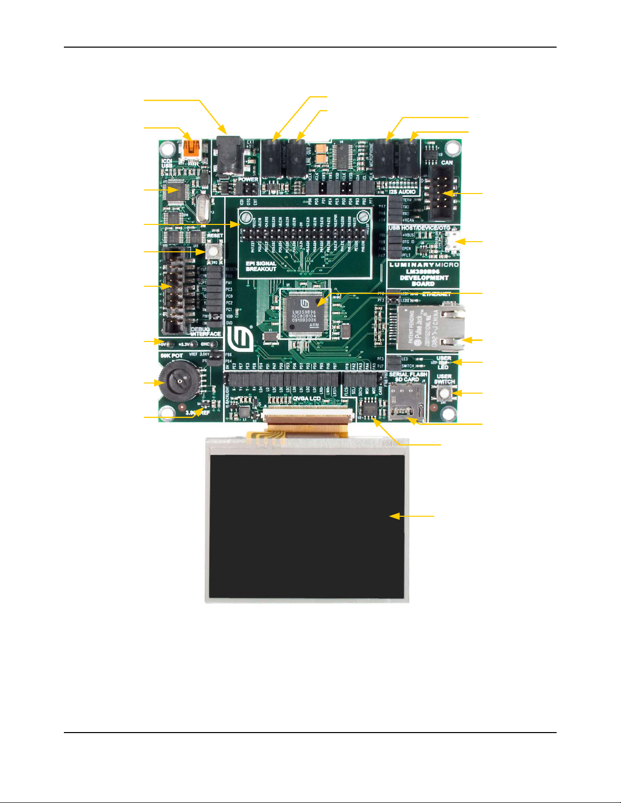
Figure 1-1. DK-LM3S9B96 Development Board
Debug I nterface
USB Connector for
Debug and/or Power
Stellaris
LM3S39B96
Microcontroller
CAN Bus Interface
3 .5 " LCD T ouc h Panel
USB connector wi th
Host, De vice an d
On-the-Go modes
10/ 100 Et hernet
User LED
microSD Card Slot
Potentiometer
5 VDC supply input
JTAG/SWD In/
Out C onnector
User Switch
Reset switch
Power and
Ground Test
Points
3 .00V Analog
Reference
Headphone Out put
Audi o Li ne Output
Microphone Input
Audi o Li ne I n put
1MB Serial Fl ash Mem ory
Stellaris® LM3S9B96 Development Kit User’s Manual
September 5, 2010 9
Page 10

Development Kit Contents
The Stellaris® LM3S9B96 Development Kit contains everything needed to develop and run a
range of applications using Stellaris microcontrollers:
LM3S9B96 development board
8 MB SDRAM expansion board
EPI signal breakout board
Retractable Ethernet cable
USB Mini-B cable for debugger use
USB Micro-B cable for OTG-to-PC connection
USB Micro-A to USB A adapter for USB Host
USB Flash memory stick
microSD Card
20-position ribbon cable
CD containing:
– A supported version of one of the following (including a toolchain-specific Quickstart
guide):
• Keil™ RealView® Microcontroller Development Kit (MDK-ARM)
• IAR Embedded Workbench
• Code Sourcery GCC development tools
• Code Red Te chnologies development tools
• Texas Instruments’ Code Composer Studio™ IDE
– Complete documentation
– Quickstart application source code
– Stellaris® Firmware Development Package with example source code
10 September 5, 2010
Page 11
Stellaris® LM3S9B96 Development Kit User’s Manual
USB
USB
USB
T
Stellaris
Tempest-cl ass
LM 3S9B96
Microcontroller
QVGA
Color LCD Module
I/O Signal Break-out
Switch
LED
Tempest LM 3S9B96 D evelo pment Bo ard
I/O Signal B reak-out
I/O signals
Dual
USB
Device
Controller
Debug
JTAG/SWD
Output/Input
Debug USB
Reset
+3.3V
Regulator
SWD/JTAG Mux
UART0
Debug
USB
Control+5V host supply
USB
micro-AB
connector
OTG/Host/Device
T
a
r
g
e
t
C
a
b
l
e
MicroSD
card slot
1GB
1MB
Serial
Flash
EPI
Touch
RJ45
Jack+
Magnetics
Ethernet
Pot
Thumb
wheel
Pot
8MB SDRAM
Headphone
Jack
Line Out
Jack
I2S
Audio
CODEC
Line Output
Phones
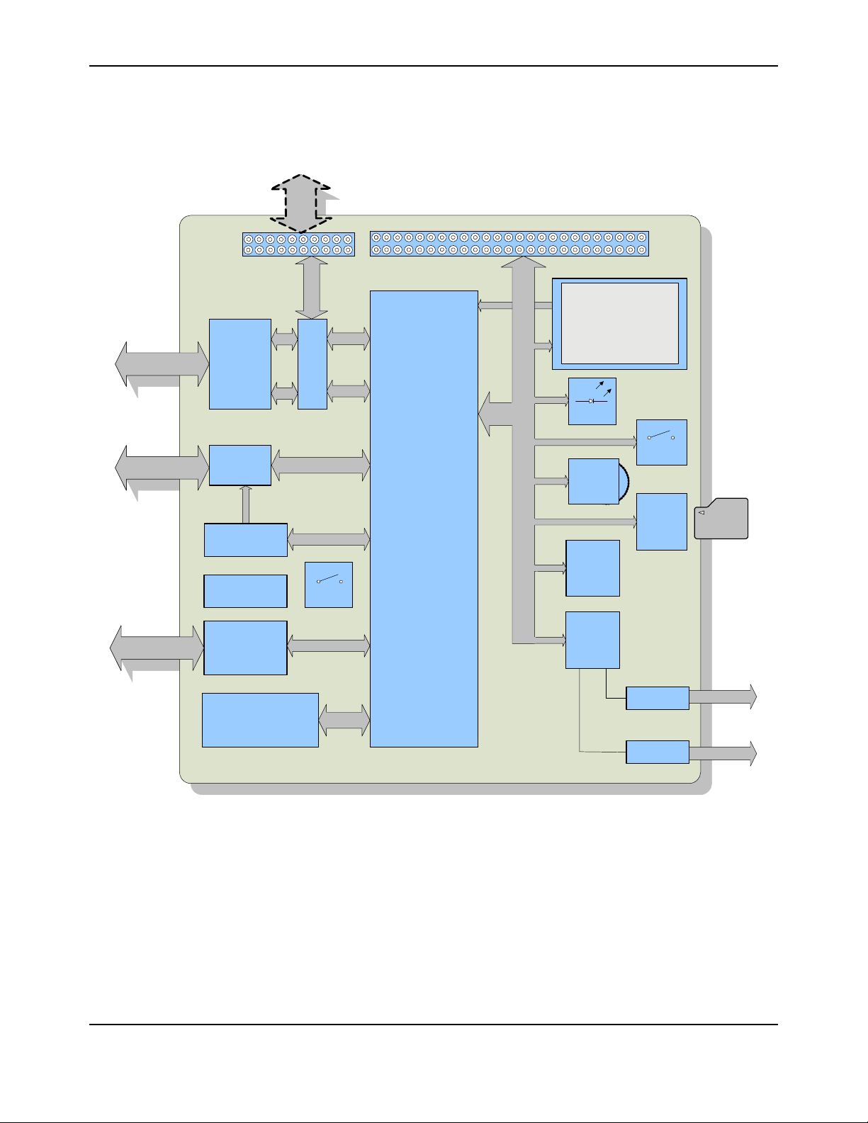
Block Diagram
Figure 1-2. DK-LM3S9B96 Development Board Block Diagram
Development Board Specifications
Board supply voltage: 4.75–5.25 Vdc from one of the following sources:
– Debugger (ICDI) USB cable (connected to a PC)
– USB Micro-B cable (connected to a PC)
– DC power jack (2.1x 5.5mm from exte rn al po we r su pp ly)
Break-out power output: 3.3 Vdc (100 mA max)
September 5, 2010 11
Page 12

Dimensions (excluding LCD panel):
– 4.50” x 4.25” x 0.60” (LxWxH) with SDRAM board
– 4.50” x 4.25” x 0.75” (LxWxH) with EPI breakout board
Analo g Re fe re nc e: 3. 0 V +/-0.2 %
RoHS status: Compliant
NOTE: When the LM3S9B96 Development Board is used in USB Host mode, the host connector
is capable of supplying power to the connected USB device. The available supply current
is limited to ~200 mA unless the development board is powered from an external 5 V
supply with a =600mA rating.
12 September 5, 2010
Page 13
CHAPTER 2
Stellaris® LM3S9B96 Development Board Hardware Description
In addition to an LM3S9B96 microcontroller, the development board includes a range of useful
peripheral features and an integrated in-circuit debug interface (ICDI). This chapter describe s how
these peripherals operate and interface to the microcontroller
LM3S9B96 Microcontroller Overview
The Stellaris LM3S9B96 is an ARM Cortex-M3-based microcontroller with 256-KB flash memory,
80-MHz operation, Ethernet, USB, EPI, SAFERTOS™ in ROM, and a wide range of peripherals.
See the LM3S9B96 Microcontroller Data Sheet (order number DS-LM3S9B96) for complete
microcontroller details.
The LM3S9B96 microcontroller is factory-programmed with a quickstart demo program. The
quickstart program resides in on-chip flash memory and runs each time power is applied, unless
the quickstart has been replaced with a user program.
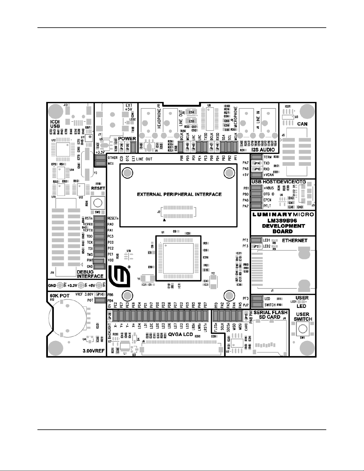
Jumpers and GPIO Assignments
Each peripheral circuit on the development board is interfaced to the LM3S9B96 microcontroller
through a 0.1” pitch jumper/shunt. Figure 2-1 on page 14 shows the fact ory default positions of the
jumpers. The jumpers must be in these positions for the quickstart demo program to function
correctly.
The development board offers capabilities that the LM3S9B96 cannot support simultaneously due
to pin count and GPIO multiplexing limitations. For example, as configured, the board does not
support SDRAM and I
jumpers associated with I
Table 2-1 lists all features and peripherals that are disconnected in the factor y de fa ult
configuration. Using these peripherals requires that other peripherals be disconnected.
Appendix D, “Stellaris® LM3S9B96 Development Board Microcontroller GPIO Assignments,” on
page 37 lists alternative jumper configurations used in conjunction with some of the
StellarisWare™ example applications for this board.
Table 2-1. Board Features and Peripherals that are Disconnected in Factory Default
Configuration
Peripheral Jumpers
2
I
S Receive (Audio Input) JP44, 45, 47, 49
Controller Area Network (CAN) JP14, 15
Ethernet Yellow Status LED (LED2) JP2
Analog 3.0V Reference JP33
See Appendix D, “Stellaris® LM3S9B96 Development Board Microcontroller GPIO Assignments,”
on page 37, for a complete list of GPIO assignments. The table lists all default and alternate
2
S receive (microphone or line input) functions at the sa me ti me . The
2
S receive are omitted in the default configuration.
September 5, 2010 13
Page 14
assignments that are supported by the 0.1” jumpers and PCB routing. The LM3S9B96 has
additional internal multiplexing that enables additional configurations which may require discrete
wiring between peripherals and GPIO pins.
The ICDI section of the board has a GND-GND jumper that serves no function other than to
provide a convenient place to ‘park’ a spare jumper. This jumper may be reused as required.
Figure 2-1. Factory Default Jumper Settings
Clocking
The development board uses a 16.0-MHz (Y2) crystal to complete the LM3S9B96
microcontroller's main internal clock circuit. An internal PLL, configured in software, multiples this
clock to higher frequencies for core and peripheral timing.
A 25.0-MHz (Y1) crystal provides an accurate timebase for the Ethernet PHY.
14 September 5, 2010
Page 15
Reset
The RESETn signal into the LM3S9B96 microcontroller connects to the reset switch (SW2) and to
the ICDI circuit for a debugger-controlled reset.
External reset is asserted (active low) under any one of the three following conditions:
Power-on reset (filtered by an R-C network)
Reset push switch SW2 held down
By the ICDI circuit (U12 FT2232, U13D 74LVC125A) when instructed by the debugger (this
capability is optional, and may not be supported by all debuggers)
The LCD module has special Reset timing requirement s requiring a ded icated control line from the
microcontroller.
Power Supplies
The development board requires a regulated 5.0 V power source. Jumpers JP34-36 select the
power source, with the default source being the ICDI USB connector . Only one +5 V source should
be selected at any time to avoid conflict between the power sources.
When using USB in Host mode, the power source should be set to either ICDI or to EXT if a +5 V
power supply (not included in the kit) is available.
Stellaris® LM3S9B96 Development Kit User’s Manual
USB
The development board has two main power rails. A +3.3 V supply powers the microcontroller and
most other circuitry. +5 V is used by the OTG USB port and In-circuit Debug Interface (ICDI) USB
controller. A low drop-out (LDO) regulator (U5) converts the +5 V power rail to +3.3 V. Both rails
are routed to test loops for easy access.
The LM3S9B96’s full-speed USB controller supports On-the-Go, Host, and Device configurations.
See Table 2-2 for USB-related signals. The 5-pin microAB OTG connector supports all three
interfaces in conjunction with the cables included in the kit.
The USB port has additional ESD protection diode arrays (D1, D2,D5) for up to 15 kV of ESD
protection.
Table 2-2. USB-Related Signals
Microcontroller Pin Board Function Jumper Name
Pin 70 USB0DM USB Data- Pin 71 USB0DP USB Data+ Pin 73 USB0RBIAS USB bias resistor Pin 66 USB0ID OTG ID signal (input to microcontroller) OTG ID
Pin 67 USB0VBUS Vbus Level monitoring +VBUS
Pin 34 USB0EPE Host power enable (active high) EPEN
Pin 35 USB0PFLT Host power fault signal (active low) PFLT
U6, a fault-protected switch, controls and monitors power to the USB host port. USB0EPEN, the
control signal from the microcontroller , has a pull-down resistor to en sure host-p ort power rema ins
off during reset. The power switch will immediately cut power if the attached USB device draws
September 5, 2010 15
Page 16
more than 1 Amp, or if the switches’ thermal limits are exceeded by a device drawing more than
500 mA. USB0PFLT indicates the over-current status back to the microcontroller.
The development board can be either a bus-po wered USB device or self-powered USB device
depending on the power-supply configuration jumpers.
When using the development board in USB-host mode, power to the EVB should be supplied by
the In-circuit Debugger (ICDI) USB cable or by a +5 V source connected to the DC power jack.
Note that the LM3S9B96’s USB capabilities are completely independent from the In-Circuit Debug
Interface USB functionality.
Debugging
Stellaris microcontrollers support programming and debugging using either JTAG or SWD. JTAG
uses the TCK, TMS, TDI, and TDO signals. SWD requires fewer signals (SWCLK, SWDIO, and,
optionally, SWO for trace). The debugger determines which debug protocol is used.
Debugging Modes
The LM3S9B96 development board supports a range of hardware debugging configurations.
Table 2-3 summarizes these configurations.
Table 2-3. Hardware Debugging Configurations
Mode Debug Function Use Selected by...
1 Internal ICDI Debug on-board LM3S9B96
2 ICDI out to JTAG/ SWD
header
3 In from JT AG/SWD header For users who prefer an
Debug In Considerations
Debug Mode 3 supports board debugging using an external debug interface such as a Segger
J-Link or Keil ULINK. Most debuggers use Pin 1 of the Debug connec to r to se nse the target
voltage and, in some cases, power the output logic circuit. Installing the VDD/PIN1 jumper will
apply 3.3 V power to this pin in order to support external debuggers.
Debug USB Overview
An FT2232 device from Future Technology Devices International Ltd implements USB-to-serial
conversion. The FT2232 is factory-configured to implement a JTAG/SWD port (synchronous
serial) on channel A and a Virtual COM Port (VCP) on channel B. This feature allows two
simultaneous communications links between the host computer an d the target device using a
single USB cable. Separate Windows drivers for each func tion are provided on the Docume ntation
and Software CD.
microcontroller over Debug
USB interface.
The development board is
used as a USB to SWD/
JTAG interface to an
external target.
external debug interface
(ULINK, JLINK, etc.) with the
development board.
Default mode
Remove jumpers on TCk,
TMS, TDI, TDO, and PIN1
Connecting an external
debugger to the JTAG/SWD
header
The In-Circuit Debug Interface USB capabilities are completely independent from the LM3S9B96’s
on-chip USB functionality.
16 September 5, 2010
Page 17
A small serial EEPROM holds the FT2232 configuration data. The EEPROM is not accessible by
the LM3S9B96 microcontroller. For full details on FT2232 operation, go to www.ftdichip.com.
USB to JTAG/SWD
The FT2232 USB device performs JT AG/SWD serial operations under th e control of the debugger.
A simple logic circuit multiplexes SWD and JTAG functions and, when working in SWD mode,
provides direction control for the bidirectional data line.
Virtual COM Port
The Virtual COM Port (VCP) allows Windows applications (such as HyperTe rm in al) to
communicate with UART0 on the LM3S9B96 over USB. Once the FT2232 VCP driver is in stalled,
Windows assigns a COM port number to the VCP channel. Table 2-4 shows the debug-related
signals.
Table 2-4. Debug-Related Signals
Microcontroller Pin Board Function Jumper Name
Pin 77 TDO/SWO JT AG data out or trace data out TDO
Pin 78 TDI JTAG data in TDI
Pin 79 TMS/SWDIO JT AG TMS or SWD data in/out TMS
Stellaris® LM3S9B96 Development Kit User’s Manual
Pin 80 TCK/SWCLK JTAG Clock or SWD clock TCK
Pin 26 PA0/U0RX Virtual Com port data to LM3S9B96 VCPRX
Pin 27 PA1/U0TX Virtual Com port data from LM3S9B96 VCPTX
Pin 64 RSTn System Reset RSTn
Serial Wire Out (SWO)
The development board supports the Cortex-M3 Serial-Wire Output (SWO) trace capabilities.
Under debugger control, on-board logic can route the SWO datastream to the VCP transmit
channel. The debugger software can then decode and interpret the trace information received
from the Virtual Com Port. The normal VCP connection to UART0 is interrupted when using SWO.
Not all debuggers support SWO.
See the Stellaris LM3S9B96 Microcontroller Data Sheet for additional information on the Trace
Port Interface Unit (TPIU).
Color QVGA LCD Touch Panel
The development board features a TFT Liquid Crystal graphics display with 320 x 240 pixel
resolution. The display is protected during shipping by a thin, protective plastic film which should
be removed before use.
Features
Features of the LCD module include:
Kitronix K350QVG-V1-F display
320 x RGB x 240 dots
3.5” 262 K colors
September 5, 2010 17
Page 18
Wide temperature range
White LED backlight
Integrated RAM
Resist ive to uc h panel
Control Interface
The Color LCD module has a built-in controller IC with a multi-mode parallel interface. The
development board uses an 8-bit 8080 type interface with GPIO Port D providing the data bus.
Table 2-4 shows the LCD-related signals.
Table 2-5. L CD-Related Signals
Microcontroller Pin Board Function Jumper Name
PE6/ADC1 Touch X+ X+
PE3 Touch Y- YPE2 Touch X- XPE7/ADC0 Touch Y+ Y+
PB7 LCD Reset LRSTn
PD0..7 LCD Data Bus 0..7 LD0..7
PH7 LCD Data/Control Select LDC
PB5 LCD Read Strobe LRDn
PH6 LCD Write Strobe LWRn
- Backlight control BLON
Backlight
The white LED backlight must be powered for the display to be clearly visible. U7 (FAN5331B)
implements a 20 mA constant-current LED power source to the backlight. The backlight is not
normally controlled by the microcontroller, however, the control signal is available on a header. A
jumper may be installed to disable the backlight by connecting it to GND. Alternatively, a wire may
be used to control this signal from a spare microcontroller GPIO line.
Because the FAN5331B operates in a constant current mode, its output voltage will jump up if the
LCD should become disconnected. To prevent over-voltage failure of the IC or diode D3, a zener
(D4) clamps the voltage. The current will limit to 20 mA, but the total board current will be higher
than when the LCD panel is connected. To avoid over-heating the backlighting circuit, install the
BLON jumper to completely shut-down the backlighting circuit.
Power
The LCD module has internal bias voltage generators and requires only a single 3.3 V dc supply.
Resistive Touch Panel
The 4-wire resistive touch panel interfaces directly to the microcontroller, using 2 ADC channe ls
and 2 GPIO signals. See the StellarisW are™ source code for additio nal information on touch panel
implementation.
18 September 5, 2010
Page 19
I2S Audio
The LM3S9B96 development board has advanced audio capabilities using an I2S-connected
Audio TLV320AIC23 CODEC. The factory default configuration has Audio output (Line Out and/or
Headphone output) enabled. Four additional I
and/or Microphone). All four audio interfaces are through 1/8” (3.5mm) stereo jacks. Table 2-6
shows the I
Table 2-6. I
Stellaris® LM3S9B96 Development Kit User’s Manual
2
S signals are required for Audio input (Line Input
2
S audio-related signals.
2
S Audio-Related Signals
Microcontroller Pin Board Function Jumper Name
I2C0SDA CODEC Configuration Data SDA
I2C0SCL CODEC Configuration Clock SCL
I2STXSD Audio Out Serial Data TXSD
I2STXWS Audio Out Framing signal TXWS
I2STXSCK Audio Out Bit Clock BCLK
I2STXMCLK Audio Out System Clock MCLK
I2SRXSD Audio In Serial Data RXSD
I2SRXWS Audio In Framing signal RXWS
I2SRXSCK Audio In Bit Clock BCLK
I2SRXMCLK Audio In System Clock MCLK
a
b
b
b
b
a. Shares GPIO line with Analog voltage reference. Jumper installed by default.
b. Shares GPIO line with LCD data bus – Port D. Jumper omitted by default.
The Audio CODEC has a number of control registers which are configured using the I
signals. CODEC settings can only be written, but not read, using I
example applications for programming information and the TLV320AIX23B data sheet for
complete register details.
The Headphone output can be connected dir ectly to any stand ard headphones. The Lin e Output is
suitable for connection to an external amplifier, including PC desktop speaker sets.
User Switch and LED
The development board provides a user push-switch and LED (see Table 2-7).
Table 2-7. Navigation Switch-Related Signals
Microcontroller Pin Board Function Jumper Name
PJ7 User Switch SWITCH
PF3 User LED LED
a. Shared with Ethernet Jack Yellow LED. This jumper is installed by default.
2
2
C. See the StellarisW are™
a
C bus
September 5, 2010 19
Page 20

20 September 5, 2010
Page 21

CHAPTER 3
Stellaris® LM3S9B96 Development Board External Peripheral Interface (EPI)
The External Peripheral Interface (EPI) is a high-speed 8/16/32- bit parallel bus for connecting
external peripherals or memory without glue logic. Supported modes include SDRAM, SRAM, and
Flash memories, as well as Host-bus and FIFO mo d es.
The LM3S9B96 development kit includes an 8 MB SDRAM board in addition to an EPI break-out
board. Other EPI expansion boards may be availabl e.
SDRAM Expansion Board
The SDRAM board provides 8 MB of memory (4M x 16) which, once configured, becomes part of
the LM3S9B96’s memory map at either 0x6000 .0 0 00 or 0x80 00 .0 00 0 . Th e SDRAM inte r face
multiplexes DQ00..14 and AD/BA0..14 without requiring external latches or buffers. Of the 32 EPI
signals, only 24 are used in SDRAM mode, with the remaining signals used for non-EPI functions
on the board.
Flash and SRAM Memory Expansion Board
The optional Flash and SRAM Memory Expansion Board (DK-LM3S9B9 6-FS8) is a plug-in fo r th e
DK-LM3S9B96 development board. This expansion board works with the External Peripheral
Interface (EPI) of the Stellari s microcontroller and provides Flash memory, SRAM, and an
improved performance LCD interface.
For more information on the Flash and SRAM Memory Expansion Board (sold separately), see
Appendix E, “Stellaris® LM3S9B96 Flash and SRAM Memory Expansion Board,” on page 41.
FPGA Expansion Board
The FPGA Expansion Board (DK-LM3S9B96-FPGA) is an optional expansion board which
connects directly to the External Peripheral Interface (EPI) port of the Stellaris DK-LM3S9B96
development board to demonstrate the machine-to-machine (M2M), high-bandwidth, parallel
interface capability of the Stellaris microcontroller. Right out of the box, users are able to control
and display the FPGA expansion board’s video on the DK- LM3S9B96 development bo ard’s large,
3.5” touchscreen display.
For more information on the FPGA Expansion Board (sold separately), see Append ix F , “S tellaris®
LM3S9B96 FPGA Expansion Board,” on page 49.
EM2 Expansion Board
The EM2 Expansion Board (DK-LM3S9B96-EM2) is an optional expansion boar d wh ich connects
directly to the External Peripheral Interface (EPI) port of the Stellaris DK-LM3S9B96 development
board. The EM2 Expansion Board provides a transition between the Stellaris External Peripheral
Interface (EPI) connector and the RF Evaluation Module (EM) connector. The DK-LM3S9B96-EM2
enables wireless application development using Low Power RF and RF ID evaluation modules on
the Stellaris DK-LM3S9B96 platform.
For more information on the EM2 Expansion Board (sold separately), see Appendix G, “Stellaris®
LM3S9B96 EM2 Expansion Board,” on page 69.
September 5, 2010 21
Page 22

22 September 5, 2010
Page 23
LM3S9B96 Dev Board
Target
Board
Stellaris
MCU
USB
to
JTAG/
SWD
PC with IDE/
debugger
Stellaris
MCU
JT AG or SW D c onnec t s to t he
ext ernal m ic roc ont roller
Rem ov e jum pers to us e I C D I Out F eat ure
`
TCK
TMS
TDI
TDO
Target
Cable
VDD
+3.3 V
CHAPTER 4
Using the In-Circuit Debugger Interface
The Stellaris® LM3S9B96 Development Kit can operate as an In-Circuit Debugger Interface
(ICDI). ICDI acts as a USB to the JTAG/SWD adaptor, allowing debugging of any external target
board that uses a S tellaris mi crocontroller. See “Debugging Modes” on page 16 for a description of
how to enter ICDI Out mode.
Figure 4-1. ICD Interface Out Mode
The debug interface operates in either serial-wire debug (SWD) or JTAG mode, depending on the
configuration in the debugger IDE.
The IDE/debugger does not distinguish between the on-board Stellaris microcontroller and an
external Stellaris microcontroller. The only requirement is that the correct Stellaris device is
selected in the project configuration.
The Stellaris target board should have a 2x10 0.1” pin header with signals as indicated in
Table C-1 on page 35. This applies to both an external Stellaris microcontroller target (Debug
Output mode) and to external JTAG/SWD debuggers (Debug Input mode).
ICDI does not control RST (device reset) or TRST (test reset) signals. Both reset functions are
implemented as commands over JTAG/SWD, so these signals are usually not necessary.
September 5, 2010 23
Page 24

24 September 5, 2010
Page 25

APPENDIX A
Stellaris® LM3S9B96 Development Board Schematics
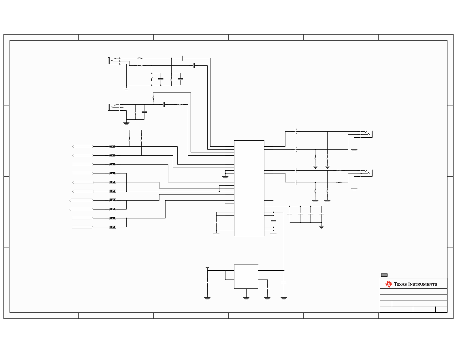
This section contains the schematics for the DK-LM3S9B96 development board.
Micro, EPI connector, USB, and Ethernet on page 26
LC D CAN, Ser i al Me m ory, and User I/O on page 2 7
Power Supplies on page 28
2
I
S Audio Expansion Board on page 29
EPI and SDRAM Expansion Boards on page 30
In-circuit Debug Interface (ICDI) on page 31
September 5, 2010 25
Page 26
1
1
2
2
3
3
4
4
5
5
6
6
D D
C C
B B
A A
Document Number:
RevSheetDate:
of
4/23/2009 1 6
Drawing Title:
Page Title:
Size
LM3S9B96 Development Board
Micro, EPI connector, USB and Ethernet
B
A
DB-LM3S9B96
10PFC110PF
C2
PC0/TCK
PC1/TMS
PC2/TDI
PC3/TDO
6
5
8
4
2
3
1
7
1CT:1
TX+
TXRX+
RX-
1CT:1
Y+
Y-
G+
G-
3
8
7
4
5
6
11
12
2
1
GL
GR
9
10
NC
GND
J1
J3011G21DNL
R6
49.9
+3.3V
R4
49.9
R5
49.9R749.9
C18
0.1UF
+3.3V
C19
0.1UF
+3.3V
C17
10pF
C13
10pF
C16
10pF
R8
330
R2
10K
M+3.3V
Stellaris Microcontroller
R9
330
+3.3V
+3.3V
PF2/LED1
1 2
Y1
25.00MHz
C14
10pF
10PFC310PF
C4
+3.3V
C5
0.1UF
PJ2/EPI18
PJ1/EPI17
PJ0/EPI16
PG7/EPI31
PC4/EPI02
PC5/EPI03
PC6/EPI04
PC7/EPI05
PE0/EPI08
PE1/EPI09
PH4/EPI10
PH5/EPI11
PG0/EPI13
C7
0.01UFC90.1UF
C11
2.2UF
PH0/EPI06
PH1/EPI07
PF4/EPI12
PH3/EPI00
PH2/EPI01
R3
9.10K
OSC1
OSC0
XTALP
XTLN
M+3.3V
PB4/ADC10/EPI23
PB5/EPI22
PA5/SSI0TX
PA4/SSI0RX
PA2/SSI0CLK
Ethernet 10/100baseT
PG1/EPI14
PF5/EPI15
Y2
16.00MHz
1
2
3
4
5
6
7
8
9
10
11
12
13
14
15
16
17
18
19
20
21
22
23
24
25 26
27
28
29
30
31
32
33
34
35
36
37
38
39
40
41
42
43
44
45
46
47
48
49
50
J2
DF12D-50DP
EPI Expansion Connector
PD2/EPI20
PD3/EPI21
PH6/EPI26
PH7/EPI27
PE2/EPI24
PE3/EPI25
PH4/EPI10
PH3/EPI00
PH2/EPI01
PH1/EPI07
PH0/EPI06
PJ1/EPI17
PB5/EPI22
PB4/ADC10/EPI23
PE2/EPI24
PE3/EPI25
PJ3/EPI19
PJ4/EPI28
PJ5/EPI29
PJ6/EPI30
PD2/EPI20
PD3/EPI21
PH7/EPI27
PJ0/EPI16
PG1/EPI14
PG0/EPI13
PC4/EPI02
PC5/EPI03
PC6/EPI04
PC7/EPI05
PH6/EPI26
PH5/EPI11
PE0/EPI08
PE1/EPI09
+3.3V
PG7/EPI31
PJ2/EPI18
PF5/EPI15
PF4/EPI12
+5V
Revision Date Description
History
0 11 Mar 09 Initial Prototype
R1
12.4K
RESETn
PJ3/EPI19
PJ4/EPI28
PJ5/EPI29
PJ6/EPI30
PA3
PA1/U0TX
PA0/U0RX
PE4/I2STXWS
PE5/I2STXSD
PE6/ADC1
PE7/ADC0
PJ7
PB0/USBID
PB1/USBVBUS
PB2/I2C0SCL
PB3/I2C0SDA
PD0/I2SRXSCK
PD4/I2SRXSD
PD6
PD7
PB6/TXSCK/AVREF
PB7/NMI
PF0
PF1/TXMCLK
LED2
JP2
PF3/LED0
VBUS D- D+ ID G
123
4G25
G1
J3
USB Micro AB
USB On-the-Go
+VBUS
PB0/USBID
OTG ID
JP4
+VBUS
JP3
PB1/USBVBUS
PA0/U0RX
26
PA1/U0TX
27
PA2/SSI0CLK
28
PA3/SSI0FSS
29
PA4/SSI0RX
30
PA5/SSI0TX
31
PC0/TCK/SWCLK
80
PC1/TMS/SWDIO
79
PC2/TDI
78
PC3/TDO/SWO
77
PC4/EPI0S02
25
PC5/EPI0S03
24
PC6/EPI0S04
23
PC7/EPI0S05
22
PD0
10
PD1
11
PD2/EPI0S20
12
PD3/EPI0S21
13
PE2/EPI0S24
95
PE3/EPI0S25
96
PD6
99
PD7
100
GND
9
PH7/EPI0S27
15
GND
21
ERBIAS
33
RST_n
64
LDO
7
OSC0
48
OSC1
49
PB0/USB0ID
66
PB1/USB0VBUS
67
USB0DM
70
USB0DP
71
PB4/EPI0S23
92
PB5/EPI0S22
91
PB6/AVREF
90
PB7/NMI
89
PB2/CCP0
72
USB0RBIAS
73
PE0/EPI0S08
74
PE1/EPI0S09
75
PE4/ADC3
6
PE5/ADC2
5
PA6/USB0EPEN
34
PA7/USB0PFLT
35
PE6/ADC1
2
PE7/ADC0
1
PF0
47
PF1
61
PF2/LED1
60
PF3/LED0
59
MDIO
58
TXON
46
TXOP
43
PF5/EPI0S15
41
PG0/EPI0S13
19
PG1/EPI0S14
18
XTLN
17
XTLP
16
PF4/EPI0S12
42
RXIP
40
RXIN
37
PG7/EPI0S31
36
PH0/EPI0S06
86
PH1/EPI0S07
85
PH2/EPI0S01
84
PH3/EPI0S00
83
VDDA
3
PD5
98
PD4
97
GNDA
4
VDD
8
VDD
20
VDD
32
VDD
44
VDD
56
VDD
68
VDD
81
VDD
93
PJ2/EPI0S18
39
GND
45
PJ6
54
GND
57
PH5/EPI0S11
63
GND
69
GND
82
PJ1/EPI0S17
87
GND
94
PJ0/EPI0S16
14
VDD25
38
PH6/EPI0S26
62
VDD25
88
PJ3
50
NC
51
PJ4
52
PJ5
53
PJ7
55
PB3
65
PH4/EPI0S10
76
U1
LM3S9B96
C6
0.01UFC80.01UF
C12
0.1UF
C10
0.1UF
M+3.3V
C15
2.2UF
C21
0.01UF
+3.3V
PD2/EPI20
PD3/EPI21
PB4/ADC10/EPI23
PB5/EPI22
PE2/EPI24
PE3/EPI25
LED1
JP1
PH6/EPI26
PH7/EPI27
PA7/USBPFLT/CAN0TX
PA6/USBEPE/CAN0RX
PD1/I2SRXWS
PD5/I2SRXMCLK
PE2/EPI24
PE3/EPI25
PD2/EPI20
PD3/EPI21
PB4/ADC10/EPI23
PB5/EPI22
PH6/EPI26
PH7/EPI27
1 2
D2
B72590D0050H160
1 2
D5
B72590D0050H160
12
D1
B72590D0050H160
Indicates factory-default jumper position.
15 Apr 09 First production release
GND
2
VIN
1
VOUT
5
PG
4
EN
3
U16
FAN2558S12X
+5V
U16 Required only for
LM3S9B96 Rev B1.
See errata.
R60
10
R61
10
R60-61 = 10 Ohms for LM3S9B96 Rev B1 (see errata)
R60,R11 = 0 Ohms for LM3S9B96 Rev C
Note:
A
Schematic page 1
Page 27
1
1
2
2
3
3
4
4
5
5
6
6
D D
C C
B B
A A
Document Number:
RevSheetDate:
of
4/23/2009 2 6
Drawing Title:
Page Title:
Size
LM3S9B96 Development Board
LCD, CAN, Serial Memory, User IO
B
A
DB-LM3S9B96
Reset
SW2
SW-B3S1000
RESETn
R19
10K
+3.3V
User Switch
R18
330
Power
+3.3V
SW1
SW-B3S1000
microSD Card Slot
N/C DATA2
1
CS DATA3
2
DI CMD
3
VDD
4
CLOCK
5
GND
6
DO DATA0
7
RSV DATA1
8
FR19FR210FR311FR4
12
J4
2908-05WB-MG
+3.3V
C24
0.1UF
+3.3V
R15
10K
R16
10K
+3.3V
+3.3V
LED2
Green
C26
0.1UF
XR
YD
XL
YU
LCD_RSTn
CSn
SPICLK
SPISDI
HSYNC
VSYNC
DCLK
AVDD
VCC
DC
RD
WR
PS0
PS1
PS2
PS3
OE
LED_K
LED_A
LD1
LD2
LD3
LD4
LD5
LD6
LD7
LD8
LD10
LD11
LD12
LD13
LD14
LD15
LD16
LD17
LCD_D0
LCD_D1
LCD_D2
LCD_D3
LCD_D4
LCD_D5
LCD_D6
LCD_D7
LD0
LD9
TOUCH_YP
TOUCH_YN
TOUCH_XP
TOUCH_XN
ILED+
2
3
4
5
6
7
8
9
10
11
12
13
14
15
16
17
18
19
20
1
M1
21
22
23
24
25
26
27
28
29
30
31
32
33
34
35
36
37
38
39
40
41
42
43
44
45
46
47
48
49
50
51
52
53
54
55
56
57
58
59
60
M2
J6
FPC_Socket_60pin
QVGA LCD Panel
R21
10K
PB7/NMI
+3.3V
Thumbwheel Potentiometer
C32
0.1UF
C29
0.1UF
QVGA LCD Panel
with touch interface
LCD_D[0..7]
C28
0.01UF
C30
0.01UF
C31
0.01UF
C33
0.01UF
+3.3V
R12
50K
ILED-
C23
0.1UF
R14
10K
+3.3V
8-bit 8080 mode
PE6/ADC1
PE3/EPI25
PE2/EPI24
PE7/ADC0
X+
JP16
Y-
JP17
X-
JP18
Y+
JP19
LD0
JP21
LD1
JP22
LD2
JP23
LD3
JP24
LD4
JP25
LD5
JP26
LD6
JP27
LD7
JP28
PD2/EPI20
PD3/EPI21
PD6
PD7
LCD_D0
LCD_D1
LCD_D2
LCD_D3
LCD_D4
LCD_D5
LCD_D6
LCD_D7
LDC
JP29
LRDn
JP30
LWRn
JP31
PH7/EPI27
PH6/EPI26
LCD_DC
LCD_RDn
LCD_WRn
R11
330
PF3/LED0
User LED
LED1
Green
POT
JP7
SWITCH
JP6
PJ7
PB4/ADC10/EPI23
LED
JP5
SI
5
SCK
6
nWP
3
nCE
1
nHOLD7VDD
8
VSS
4
SO
2
U2
W25X80AVSSIG-ND
C25
0.1UF
+3.3V+3.3V
R13
10K
+3.3V
1MB Serial Flash
PA5/SSI0TX
PA2/SSI0CLK
PA4/SSI0RX
PA3
SDCSn
JP9
MOSI
JP10
SCLK
JP11
MISO
JP12
FLCSn
JP8
PF0
SD_CSn
MOSI
MISO
SSICLK
FLASH_CSn
CANH
7
CANL
6
TXD
1
RXD
4
RS
8
GND2VREF
5
VCC
3
U3
SN65HVD1050D
+5V
CAN Transceiver
C27
0.1UF
TXD
JP14
RXD
JP15
1 2
3 4
5 6
7 8
9 10
J5
CANH
CANL
VREF_3.0V
PA7/USBPFLT/CAN0TX
PA6/USBEPE/CAN0RX
R17
10K
LRSTn
JP20
R20
10K
+3.3V
R10
10K
+3.3V
PD1/I2SRXWS
CARD
JP13
PD4/I2SRXSD
PD5/I2SRXMCLK
PB5/EPI22
+VCAN
JP32
+5V
CAN Connector
+VCAN
PD0/I2SRXSCK
TERM
JP58
R58
120
C22
0.1UF
Indicates factory-default jumper position.
R59
100
Schematic page 2
Page 28

1
1
2
2
3
3
4
4
5
5
6
6
D D
C C
B B
A A
Document Number:
RevSheetDate:
of
4/23/2009 3 6
Drawing Title:
Page Title:
Size
LM3S9B96 Development Board
Power Supplies
B
A
DB-LM3S9B96
DBG+5V
VBUS Fault Protected Switch
+VBUS
GND
2
IN
5
EN
4
OCn
3
OUT
1
U6
TPS2051BDBV
C40
2.2UF
C41
2.2UF
C43
2.2UF
SHDN
4
VIN5SW
1
GND
2
FB
3
U7
FAN5333B
ILED+
D3
FYV0704SMTF
+5V
C38
2.2UF
10uH
L1
NR4018T100M
LED Backlight Controller
C45
0.1UF
C46
0.1UF
C44
0.1UF
R26
15
R25
10K
ILED-
24V
D4
BZT52C24
+5V
EPEN
JP37
PFLT
JP38
Backlight
JP39
PA7/USBPFLT/CAN0TX
PA6/USBEPE/CAN0RX
USB0EPE
USB0PFLT
0.01UF
C39
C42
2.2UF
C37
2.2UF
VOUT
5
NR
1
ON
3
GND
2
VIN
4
U5
PQ1LA333MSPQ
C36
2.2UF
+5V
ICDI
JP34
OTG
JP35
EXT
JP36
+5V
+5V DC INPUT
PJ-002BH-SMT
1
2
3
J7
+VBUS
CATHODE
1
ANODE
2
NC
3
U4
LM4040B30IDB
VREF 3.00V
JP33
R22
1.5K
+3.3V
C35
2.2UF
3.0V 0.2% Voltage Reference
Main +3.3V Supply
Power Source Selection
R24
10K
R23
10K
+3.3V
VREF_3.0V
PB6/TXSCK/AVREF
C34
0.1UF
GND
TP2
BLON
5.0V
TP3
+5V
C20
0.1UF
Indicates factory-default jumper position.
+3.3V
3.3V
TP1
P3V
JP60
M3V
JP61
M+3.3V
GND
JP59
Schematic page 3
Page 29
1
1
2
2
3
3
4
4
5
5
6
6
D D
C C
B B
A A
Document Number:
RevSheetDate:
of
4/23/2009 4 6
Drawing Title:
Page Title:
Size
LM3S9B96 Development Board
I2S Audio Expansion Board
B
A
DB-LM3S9B96
1
3
2
J11
STX-3000
BVDD
1
BCLK
3
DOUT
6
DIN
4
LRCIN
5
LRCOUT
7
CLKOUT
2
HPVDD
8
LHPOUT
9
RHPOUT
10
HPGND
11
LOUT
12
ROUT
13
AVDD
14
AGND
15
VMID
16
MICBIAS
17
MICIN
18
RLINEIN
19
LLINEIN
20
nCS
21
MODE
22
SDIN
23
SCLK
24
XTI/MCLK
25
XTO
26
DVDD
27
DGND
28
U8
TLV320AIC23BPW
C57
0.47UF
C58
0.47UF
R33
47K
R35
47K
R36
100
R37
100
Audio Line Output
1
3
2
J10
STX-3000
4V
+
C55
220UF
4V
+
C54
220UF
R32
47K
R34
47K
C56
0.1UF
C59
2.2UF
C60
2.2UF
C61
2.2UF
C50
0.1UF
1
3
2
J9
STX-3000
R31
4.7K
R28
10K
27PF
C47
C48
2.2UF
MICIN
R30
10K
MICBIAS
Audio Headphone Output
Microphone Input
MCLK
LRC
RXSD
BITCLK
TXSD
Analog +3.3V 50mA Power Supply
C52
0.1UF
Line Input
SDA
JP40
PB3/I2C0SDA
PB2/I2C0SCL
PE5/I2STXSD
PE4/I2STXWS
PD4/I2SRXSD
PD1/I2SRXWS
PF1/TXMCLK
SCL
JP41
TXSD
JP42
TXWS
JP43
RXSD
JP44
RXWS
JP45
PB6/BCLK
JP46
0.01UF
C51
C53
2.2UF
C49
2.2UF
VOUT
5
NR
1
ON
3
GND
2
VIN
4
U9
PQ1LA333MSPQ
+5V
R27
4.7K
R29
4.7K
+3.3V +3.3V
PD5/I2SRXMCLK
PB6/TXSCK/AVREF
PD0/BCLK
JP47
PD0/I2SRXSCK
1
3
2
J8
STX-3000
R54
4.7K
R55
4.7K
R56
4.7K
R57
4.7K
27PF
C76
27PF
C78
C77
0.47UF
C79
0.47UF
PD5/MCLK
JP49
PF1/MCLK
JP48
Indicates factory-default jumper position.
Rework 2: Loop TXWS to RXWS.
Schematic page 4
Page 30
1
1
2
2
3
3
4
4
5
5
6
6
D D
C C
B B
A A
Document Number:
RevSheetDate:
of
4/23/2009 5 6
Drawing Title:
Page Title:
Size
LM3S9B96 Development Board
EPI and SDRAM Expansion Boards
B
A
DB-LM3S9B96
A0
23
DQ0
2
BA0
20
BA1
21
CLK
38
CKE
37
WE
16
DQMH
39
NC
40
RAS
18
CAS
17
VSS
28
VSSQ
6
VSSQ
12
VSSQ
46
VSSQ
52
VSS
41
VSS
54
VDDQ
3
VDDQ
9
VDDQ
43
VDDQ
49
VDD
1
VDD
14
VDD
27
A1
24
A2
25
A3
26
A4
29
A5
30
A6
31
A7
32
A8
33
A9
34
A10
22
A11
35
NC
36
DQ1
4
DQ2
5
DQ3
7
DQ4
8
DQ5
10
DQ6
11
DQ7
13
DQ8
42
DQ9
44
DQ10
45
DQ11
47
DQ12
48
DQ13
50
DQ14
51
DQ15
53
CS
19
DQML
15
U10
MT48LC4M16A2
AD0
AD1
AD2
AD3
AD4
AD5
AD6
AD7
AD8
AD9
AD10
AD11
D12
BA0/D13
BA1/D14
D15
AD8
AD9
AD10
AD11
CSn
WEn
RASn
CASn
SDCLK
SDCKE
DQM1
DQM0
BA0/D13
BA1/D14
AD0
AD1
AD2
AD3
AD4
AD5
AD6
AD7
+3.3V
8MB SDRAM
C65
0.1UF
C64
0.01UF
C63
0.01UF
C66
0.1UF
+3.3V
Expansion Connector
SDRAM Expansion Board
1
2
3
4
5
6
7
8
9
10
11
12
13
14
15
16
17
18
19
20
21
22
23
24
2526
27
28
29
30
31
32
33
34
35
36
37
38
39
40
41
42
43
44
45
46
47
48
49
50
J12
DF12A-50DS
+3.3V
C62
2.2UF
AD2
AD3
AD4
AD5
SDCLK
CASn
D15
D12
AD9
AD8
AD11
BA0/D13
BA1/D14
DQM0
SDCKE
CSn
WEn
RASn
DQM1
AD6
AD7
AD1
AD0
AD10
Expansion Connector
1
2
3
4
5
6
7
8
9
10
11
12
13
14
15
16
17
18
19
20
21
22
23
24
2526
27
28
29
30
31
32
33
34
35
36
37
38
39
40
41
42
43
44
45
46
47
48
49
50
J15
DF12A-50DS
EPI Signal Breakout Board
X_PH4/EPI10
X_PH3/EPI00
X_PH2/EPI01
X_PH1/EPI07
X_PH0/EPI06
X_PJ1/EPI17
X_PB5/EPI22
X_PB4/EPI23
X_PE2/EPI24
X_PE3/EPI25
X_PJ3/EPI19
X_PJ4/EPI28
X_PJ5/EPI29
X_PJ6/EPI30
X_PD2/EPI20
X_PD3/EPI21
X_PH7/EPI27
X_PJ0/EPI16
X_PG1/EPI14
X_PG0/EPI13X_PC4/EPI02
X_PC5/EPI03
X_PC6/EPI04
X_PC7/EPI05
X_PH6/EPI26
X_PH5/EPI11
X_PE0/EPI08
X_PE1/EPI09
X_PG7/EPI31
X_PJ2/EPI18
X_PF5/EPI15
X_PF4/EPI12
X+3.3V
X+5V
Schematic page 5
Page 31
1
1
2
2
3
3
4
4
5
5
6
6
D D
C C
B B
A A
Document Number:
RevSheetDate:
of
4/23/2009 6 6
Drawing Title:
Page Title:
Size
LM3S9B96 Development Board
In-circuit Debug Interface (ICDI)
B
A
DB-LM3S9B96
GND
18
GND
25
GND
34
ADBUS0
24
ADBUS1
23
ADBUS2
22
ADBUS3
21
ADBUS4
20
ADBUS5
19
ADBUS6
17
ADBUS7
16
ACBUS0
15
ACBUS1
13
ACBUS2
12
ACBUS3
11
BDBUS0
40
BDBUS1
39
BDBUS2
38
BDBUS3
37
BDBUS4
36
BDBUS5
35
BDBUS6
33
BDBUS7
32
BCBUS0
30
BCBUS1
29
BCBUS2
28
BCBUS3
27
SI/WUA
10
SI/WUB
26
GND
9
AGND
45
VCC
3
VCC
42
VCCIOA
14
VCCIOB
31
AVCC
46
PWREN#
41
XTOUT
44
XTIN
43
EECS
48
EESK
1
EEDATA
2
TEST
47
RESET#
4
RSTOUT#
5
3V3OUT
6
USBDM
8
USBDP
7
U12
FT2232D
+3.3V
DBG+5V
R41 27
R42 27
+3.3V
+3.3V
DBG_JTAG_EN
R39
10K
R40
1.5K
R44
1.5K
R45
330
+5V
+5V
+5V+5V
FT_TCK
FT_TDI/DI
FT_TDO/DO
FT_TMS/OUTEN
0.1UF
C71
0.1UF
C72
0.1UF
C73
0.1UF
C74
0.1UF
C75
0.1UF
C70
USB Device Controller
Channel A : JTAG / SW Debug
Channel B : Virtual Com Port
5V D- D+ ID G
123
475
6
J13
54819-0572
FT_SRSTN
Debugger USB Interface
R43
USBSH
CS
1
SK
2
DI
3
DO
4
GND
5
ORG
6
NC
7
VCC
8
1K 64X16
U11
CAT93C46
1 2
Y3
6.00MHz
27PF
C68
27PF
C69
SWO_EN
0.01UF
C67
2 3
1
U14A
SN74LVC125A
5 6
4
U13B
SN74LVC125A
98
10
U13C
SN74LVC125A
12 11
13
U14D
SN74LVC125A
2 3
1
U13A
SN74LVC125A
56
4
U14B
SN74LVC125A
9 8
10
U14C
SN74LVC125A
2 3
1
U15A
SN74LVC126A
5 6
4
U15B
SN74LVC126A
98
10
U15C
SN74LVC126A
1211
13
U15D
SN74LVC126A
VCP_TX_SWO
DBGENn
12 11
13
U13D
SN74LVC125A
12
34
56
78
910
1112
1314
1516
1718
1920
J14
2X10 HDR-SHRD
+3.3V
TDI
TCK
R46
27
TMS_SWDIO
SRSTN
TDO_SWO
VCP_TX
R47
27
R48
27
R49
27
R50
27
PIN1
JP57
TCK
JP50
PC0/TCK
PC1/TMS
PC2/TDI
PC3/TDO
TMS
JP51
TDI
JP52
TDO
JP53
TCK
TDI
TMS_SWDIO
TDO_SWO
TDI
TMS_SWDIO
TCK
TDO_SWO
SRSTN
R38
10K
+3.3v
RESETn
RSTn
JP54
SRSTN
PA1/U0TX
VCPTX
JP55
PA0/U0RX
VCPRX
JP56
VCP_RX
VCP_RX
VCP_TX
JTAG/SWD In/Out
147
VCC
GND
U14E
SN74LVC125A
147
VCC
GND
U13E
SN74LVC125A
147
VCC
GND
U15E
SN74LVC126A
+3.3V +3.3V +3.3V
0.1UF
C80
+3.3V
R51
10K
+3.3V
R52
10K
R53
10K
Indicates factory-default jumper position.
Schematic page 6
Page 32

32 September 5, 2010
Page 33

APPENDIX B
Stellaris® LM3S9B96 Development Board Component Locations
This appendix contains details on compo nent locations, including:
Component placement plot for top (Figure B-1)
September 5, 2010 33
Page 34

Figure B-1. Component Placement Plot for Top
34 September 5, 2010
Page 35

Center Positive (+)
APPENDIX C
Stellaris® LM3S9B96 Development Board Connection Details
This appendix contains the following sections:
DC Power Jack (see page 35)
ARM Target Pinout (see page 35)
DC Power Jack
The EVB provides a DC power jack for connecting an external +5 V regulated (+/-5%) power
source.
The socket is 5.5 mm dia with a 2.1 mm pin.
ARM Target Pinout
In ICDI input and output mode, the Stellaris® LM3S9B96 Development Kit supports ARM’s
standard 20-pin JTAG/SWD configuration. The same pin configuration can be used for debugging
over serial-wire debug (SWD) and JTAG interfaces.
Table C-1. Debug Interface Pin Assignments
Function Pin Number
TDI 5
TDO/SWO 13
TMS/SWDIO 7
TCK/SWCLK 9
System Reset 15
VDD 1
GND 4, 6, 8, 10, 12, 14, 16, 18, 20
No Connect 2, 3, 11, 17, 19
Insert Jumper VDD/PIN1 Jumper (JP57) only wh en using th e d evelo pme nt boar d with a n exter na l
debug interface such as a ULINK or JLINK.
September 5, 2010 35
Page 36

36 September 5, 2010
Page 37

APPENDIX D
Stellaris® LM3S9B96 Development Board Microcontroller GPIO Assignments
Table D-1 shows the pin assignments for the LM3S9B96 microcontroller.
Table D-1. Microcontroller GPIO Assignments
LM3S9B96 GPIO Pin Development Board Use
Number Description Default Function Default Use Alt. Function Alternate Use
26 PA0 U0Rx Virtual Com Port
27 PA1 U0Tx Virtual Com Port
28 PA2 SSI0Clk SPI
29 PA3 SSI0Fss SD Card CSn
30 PA4 SSI0Rx SPI
31 PA5 SSI0Tx SPI
34 PA6 USB0EPEN USB Pwr Enable CAN0RX
35 PA7 USB0PFLT USB Pwr Fault CAN0TX
66 PB0 USB0ID USB OTG ID
67 PB1 USB0VBUS USB Vbus
72 PB2 I2C0SCL Audio I2C
65 PB3 I2C0SDA Audio I2C
92 PB4 ADC10 Potentiometer EPI0S23 EPI Breakout
91 PB5 PB5 LCD RDn EPI0S22 EPI Breakout
90 PB6 PB6 I2STXSCK AVREF Ext Volt Ref
89 PB7 PB7 LCD RST
80 PC0 TCK/SWCLK JTAG
79 PC1 TMS/SWDIO JTAG
78 PC2 TDI JTAG
77 PC3 TDO/SWO JTAG
25 PC4 EPI0S2 SDRAM D02 EPI0S02
24 PC5 EPI0S3 SDRAM D03 EPI0S03
23 PC6 EPI0S4 SDRAM D04 EPI0S04
22 PC7 EPI0S5 SDRAM D05 EPI0S05
September 5, 2010 37
Page 38

Table D-1. Microcontroller GPIO Assignments (Continued)
LM3S9B96 GPIO Pin Development Board Use
Number Description Default Function Default Use Alt. Function Alternate Use
10 PD0 PD0 LCD Data 0 I2SRXSCK I2S Audio In
11 PD1 PD1 LCD Data 1 I2S0RXWS I2S Audio In
12 PD2 PD2 LCD Data 2 EPI0S20 EPI Breakout
13 PD3 PD3 LCD Data 3 EPI0S21 EPI Breakout
97 PD4 PD4 LCD Data 4 I2SRXSD I2S Audio In
98 PD5 PD5 LCD Data 5 I2SRXMCLK I2S Audio In
99 PD6 PD6 LCD Data 6
100 PD7 PD7 LCD Data 7
74 PE0 EPI0S8 SDRAM D8 EPI0S08
75 PE1 EPI0S9 SDRAM D9 EPI0S09
95 PE2 PE2 Touch XN EPI0S24
96 PE3 PE3 Touch YN EPI0S25
6 PE4 I2STXWS I2S Audio Out
5 PE5 I2STXSD I2S Audio Out
2 PE6 ADC1 ADC Touch XP
1 PE7 ADC0 ADC Touch YP
47 PF0 PF0 Flash CSn
61 PF1 I2STXMCLK I2S Audio Out
60 PF2 LED1 Green Enet LED
59 PF3 PF3 User LED LED0 Yw Enet LED
42 PF4 EPI0S12 SDRAM D12
41 PF5 EPI0S15 SDRAM D15
19 PG0 EPI0S13 SDRAM D13
18 PG1 EPI0S14 SDRAM D14
36 PG7 EPI0S31 SDRAM CLK
86 PH0 EPI0S06 SDRAM D06
85 PH1 EPI0S07 SDRAM D07
84 PH2 EPI0S01 SDRAM D01
83 PH3 EPI0S00 SDRAM D00
76 PH4 EPI0S10 SDRAM D10
38 September 5, 2010
Page 39
Stellaris® LM3S9B96 Development Kit User’s Manual
Table D-1. Microcontroller GPIO Assignments (Continued)
LM3S9B96 GPIO Pin Development Board Use
Number Description Default Function Default Use Alt. Function Alternate Use
63 PH5 EPI0S11 SDRAM D11
62 PH6 EPI0S26 LCD_WRn EPI0S26 EPI Breakout
15 PH7 EPI0S27 LCD_DC EPI0S27 EPI Breakout
14 PJ0 EPI0S16 SDRAM DQM
87 PJ1 EPI0S17 SDRAM DQM
39 PJ2 EPI0S18 SDRAM CAS
50 PJ3 EPI0S19 SDRAM RAS
52 PJ4 EPI0S28 SDRAM WEn
53 PJ5 EPI0S29 SDRAM CSn
54 PJ6 EPI0S30 SDRAM SDCKE
55 PJ7 PJ7 User Switch
September 5, 2010 39
Page 40

40 September 5, 2010
Page 41
APPENDIX E
Stellaris® LM3S9B96 Flash and SRAM Memory Expansion Board
This document describes the Flash and SRAM memory expansion board
(DK-LM3S9B96-EXP-FS8) plug-in for the DK-LM3S9B96 development board. This expansion
board works with the External Peripheral Interface (EPI) port of the Stellaris microcontroller and
provides Flash memory, SRAM, and an improved performance LCD interface.
Figure E-1. Flash and SRAM Memory Expansion Board
Features
The DK-LM3S9B96-EXP-FS8 memory expansion board has the following features:
8 Megabytes of Flash memory
1 Megabyte of SRAM
Memory-mapped LCD I/F for improved LCD performance
1 kilobit of I
Power LED indicator
2
C memory for storing configuration data
Installation
To install the expansion board on the DK-LM3S9B96 development board, do the following:
1. Remove the DK-LM3S9B96-EXP-FS8 memory expansion board from the antistatic bag.
2. On the DK-LM3S9B96 board, remove any installed board on EPI connector J2.
September 5, 2010 41
Page 42

3. On the DK-LM3S9B96 board remove the shunt jumpers on JP16-JP31 and the JP39 headers
Remove board
Remove jumpers
as shown in Figure E-1 on page 41.
Figure E-2. Removing EPI Board from DK-LM3S9B96 Development Board
4. Install the two snap-in nylon standoffs on mounting holes above the EPI connector J2.
5. Place the expansion board on top of the DK-LM3S9B96 board a nd align the st andof fs, the EPI
connector, and the 2x17 J2 header.
6. Press firmly downward until the board snaps in, then verify that the board is firmly seated on
the EPI connector, the 2x17 header, and the standoffs.
7. When powering up the board, verify that the power indicator LED D1 is lit.
42 September 5, 2010
Page 43

Stellaris® LM3S9B96 Development Kit User’s Manual
MA[7:0]
MAD[7:0]
EPI[27:8]
EPI[7:0]
OEn
WRn
EPI30
EPI
Connector
FLASH/ SRAM/LCD I F Boa r d
DQ
L
MA[27:8]
ALE
MA27
EPI29
EPI28
MAD[7:0]
A
D
SRAM
WE
OE
1MB
A
D
FLASH
WE
CS
OE
8MB
LCD
Connector
LCD Control
LCD
DECODE
LCD Data
CE2
MA27
MA26
CE1
Hardware Description
The Flash and SRAM memory expansion board is designed for use with the Stellaris EPI module
configured in Host Bus 8 address/data multiplexed mode. This mode requires the use of an
external 8-bit latch for storing the lower 8 address lines A[7:0] transmitted durin g the address
phase of an EPI transfer. This latch can be seen on the expansion board block diagram shown in
Figure E-3.
Figure E-3. Flash/SRAM/LCD IF Expansion Board Block Diagram
Functional Description
The Flash and SRAM memory expansion board schematics are described in this section. The first
Flash/SRAM (Schematic 1 on page 47)
September 5, 2010 43
page of the schematics shows the memory devices and address latch part of the design. The
second page shows the LCD I/F and regulator.
Page 1 of the schematics shows the EPI connector, address latch, and memory devices.
EPI Connector
The EPI connector J1 is a 50-pin receptacle with 0.5 mm pitch that plugs into the EPI he ad e r on
the DK-LM3S9B96 board. The 32 EPI signals and the 2 I
provided on this connector . It also provides 5 V for the on-board DC regulator. Note that not all EPI
signals are used in this design.
2
C0 signals from the LM3S9B96 are
Page 44

8-bit Latch
This 8-bit latch is used to store the lower 8-bits of the address, which are transmitted during the
address phase of an EPI transfer. The EPI must be configured in Host bus 8 mode 0 mode (HB8
ADMUX), with EPI30 configured as an Address Latch Enable (ALE) signal to control this latch.
Flash Memory
The Flash memory used is a 64 Mbit, 90-nsec Spansion S29GL064N90TFI040. This 8/16 bit
memory is used in 8-bit mode. Note that MA27 is used as a chip select signal for this memory.
SRAM
The SRAM used is an 8 Mbit, 45 nsec Cypress Semiconductor CY62158EV30LL-45ZSX, which is
an 8-bit memory. Note that MA27 and MA26 are used as chip selects for this memory.
2
I
C Memory
2
This I
C serial memory is used for storing configuration data. This is a 1 kilobit On-Semiconductor
memory.
LCD I/F, Power (Schematic 2 on page 48)
Page 2 of the schematics shows the LCD_DECODE CPLD, LCD interface connector, and the
3.3 V regulator.
LCD_DECODE CPLD
The LCD DECODE CPLD provides address latch and decode for the LCD interface. The LCD
Command and Data registers are mapped on the EPI memory space to streamline access to
these registers. The LCD panel control signals L_RDn, L_RWn, and L_DC and the L_D bus are
controlled by decode logic on the CPLD with timing derived from EPI signals and do not require
direct control from the microcontroller . The LCD latch register is provided to control the XN and YN
signals used for the touchscreen and also the reset signal to the LCD.
The LCD backlight signal L_BL is controlled by the Stellaris GPIO PE2 (MA[24]). PE2 can be
programmed as a GPIO for ON/OFF control of the LCD. A second option is to configure PE2 for
use as CCP2 or CCP4 with a PWM output for brightness control.
The TP1-TP4 testpoints connect to the CPLD JTAG signals and, along with TP5 and TP6, provide
an interface for test and programming of the CPLD.
LCD Interface Connector
The LCD Interface Connector J2 is a 2x17 socket that connects to headers JP16-JP31 and JP39
on the DK-LM3S9B96. All signals previously driven to the LCD from the Stellaris MCU are
replaced by equivalent signals driven from the LCD_DECODE CPLD.
DC Regulator
DC regulator U4 receives 5 V from the EPI connector and provides 3.3 V for the board. LED D1
provides a power indicator and lights when the regulator is providing power to the board.
44 September 5, 2010
Page 45

Stellaris® LM3S9B96 Development Kit User’s Manual
Memory Map
The DK-LM3S9B96-EXP-FS8 expansion boa rd memo ry ma p is shown in Table E-1 and T a ble E-2
shows the LCD Latch register.
Table E-1. Flash and SRAM Memory Expansion Board Memory Map
Device A[27:26] A[2:0] Description Access Base address
FLASH 0X XXX Flash memory (8 Megabytes) R/W 0x6000.0000
SRAM 10 XXX SRAM (1 Megabyte) R/W 0x6800.0000
CPLD
LCD
LCD
a. For reads to the LCD Command and Data Port registers, the corresponding LCD Port Read Start register must be read first,
followed by a 500 nsec delay before reading this register.
11 000
11 001
11 010
11 011
11 110
11 111
Table E-2. LCD Latch Register
LCD latch set R/W 0x6C00.0000
LCD latch clear R/W 0x6C00.0001
LCD command port Ra/W
LCD data port Ra/W 0x6C00.0003
LCD command port read start R 0x6C00.0006
LCD data port read start R 0x6C00.0007
0x6C00.0002
7 6 5 4 3 2 1 0
Reserved RST YN XN
0 0 0 0 0 R/W R/W R/W
The LCD Latch register is implemented as a set/clear register. To set a bit, the corresponding bit
must be set when writing to the LCD Latch Set register. To clear a bit, the corresponding bit must
be set when writing to the LCD Latch Clear register.
XN When clear, the L_XN signal is set to clear. When set, the L_XN signal is tri-stated. This
signal is used for the X- input to the touchscreen.
YN When clear, the L_YN signal is set to clear. When set, the L_YN signal is tri-stated. This
signal is used for the Y- input to the touchscreen.
RST When clear, the L_RSTN signal is set to clear. When set, the L_RSTN signal is reset. This
signal is used to reset the LCD panel.
September 5, 2010 45
Page 46

Component Locations
Top Bottom
Figure E-4 shows the details of the component locations.
Figure E-4. Component Placement Plot for Top and Bottom
Schematics
This section shows the schematics for the DK-LM3S9B96-EXP-FS8 memory expansion board:
Flash, SRAM on page 47
LCD Interface on page 48
46 September 5, 2010
Page 47

1
1
2
2
3
3
4
4
5
5
6
6
D D
C C
B B
A A
Document Number: Rev
SheetDate: of
7/21/2009
12
B
Designer:
Drawn by:
Approved:
Drawing Title:
Page Title:
Size
Arnaldo Cruz
Arnaldo Cruz
*
0001
FLASH / S RAM / LCD IF board fo r D K -L M3S9B96
FLASH, S RAM
B
108 Wild Basin Rd.
Suite 350
Austin, TX 78746
TI AEC - Austin
Revision History
Revision
A 5/29/2009
Released for manufacturing.
Date Description
3.3V
MA0
MA1
MA2
MA3
MA4
MA5
MA6
MA7
MA8
MA9
MA10
MA11
MA12
MA13
MA14
MA15
MA16
MA17
MA18
MAD0
MAD1
MAD2
MAD3
MAD4
MAD5
MAD6
MAD7
R2 10K
PG0/EPI13
PG1/EPI14
PH7/EPI27
PJ0/EPI16
PD3/EPI21
PD2/EPI20
PJ6/EPI30
PJ5/EPI29
PJ4/EPI28
PJ3/EPI19
PE3/EPI25
PE2/EPI24
PB4/EPI23
PB5/EPI22
PJ1/EPI17
PH0/EPI6
PH1/EPI7
PH2/EPI1
PH3/EPI0
PH4/EPI10
1
2
3
4
5
6
7
8
9
10
11
12
13
14
15
16
17
18
19
20
21
22
23
24
2526
27
28
29
30
31
32
33
34
35
36
37
38
39
40
41
42
43
44
45
46
47
48
49
50
J1
DF12A-50DS
PC4/EPI2
PC5/EPI3
PC6/EPI4
PC7/EPI5
PG7/EPI31
PJ2/EPI18
PF5/EPI15
PF4/EPI12
PE1/EPI9
PE0/EPI8
PH5/EPI11
PH6/EPI26
3.3V
3.3V5V
MA8
MA9
MA10
MA11
MA12
MA13
MA14
MA15
MA16
MA17
MA18
MA19
MA20
MA21
MA22
MA23
MA24
MA25
MA26
MAD0
MAD1
MAD2
MAD3
MAD4
MAD5
MAD6
MAD7
TP7
3.3V
MA0
MA1
MA2
MA3
MA4
MA5
MA6
MA7
MA8
MA9
MA10
MA11
MA12
MA13
MA14
MA15
MA16
MA27
TP8
ALE
R1 0
C4
0.1uFC50.1uF
C1
0.1uF
3.3V
C10
0.1uF
R5 2.80k
3.3V
R6 2.80k
I2CSCL
I2CSDA
MA19
MA20
MA21
MA22
MAD0
MAD1
MAD2
MAD3
MAD4
MAD5
MAD6
MAD7
A0
5
DQ0
9
A1
4
A2
3
A3
2
A4
1
A5
44
A6
43
A7
42
A8
39
A9
28
A10
27
A11
26
A12
25
DQ1
10
DQ2
13
DQ3
14
DQ4
31
DQ5
32
DQ6
35
DQ7
36
A13
24
A14
23
A15
22
A16
21
A17
20
WE
17
OE
41
CE1
6
VSS
12
VSS
34
VCC
11
8Mbit
CE2
40
NC
7
NC
8
NC
15
NC
16
NC
29
NC
30
NC
37
NC
38
A19
18
A18
19
VCC
33
U2
CY62158EV30
MA0
MA1
MA2
MA3
MA4
MA5
MA6
MA7
3.3V
C12
0.1uF
MAD0
MAD1
MAD2
MAD3
MAD4
MAD5
MAD6
MAD7
MA17
MA18
MA19
MA26
MA27
MA27
EPI I/F
3.3V
R4
10K
C11
0.1uF
Decode Table
Device
FLASH 0X
MA[27:26]
SRAM
LCD
10
11
GND10VCC
20
D1
3
D2
4
D3
7
D4
8
D5
13
D6
14
D7
17
D8
18
Q1
2
Q2
5
Q3
6
Q4
9
Q5
12
Q6
15
Q7
16
Q8
19
OE
1
LE
11
U3
74LVC373
Flash memory
SRAM memory
LCD Latch/Port
Description
MAD[7..0]
MA[27..0]
MAD[7..0]
MA[27..0]
MOEn
MWEn
MOEn
MWEn
MWEn
MOEn
F_RSTn
R3
10K
3.3V
ALE
A0
1
A1
2
A2
3
SDA
5
GND
4
SCL
6
WP
7
VCC
8
1K - 128X8
U5
CAT24C01
FLASH
SRAM
Note: R1 is not fitted
B 7/17/2009
Changed J2 to top entry, moved to bottom. Added R9-R11.
A0
25
DQ0
29
A1
24
A2
23
A3
22
A4
21
A5
20
A6
19
A7
18
A8
8
A9
7
A10
6
A11
5
A12
4
DQ1
31
DQ2
33
DQ3
35
DQ4
38
DQ5
40
DQ6
42
DQ7
44
A13
3
A14
2
A15
1
A16
48
A17
17
RDY
15
WE
11
OE
28
CE
26
VSS
27
VSS
46
VCC
37
64Mbit
BYTE
47
DQ8
30
DQ9
32
DQ10
34
DQ11
36
DQ12
39
DQ13
41
DQ14
43
DQ15/A-1
45
RP
12
A18
16
A19
9
A20
10
A21
13
VPP/WP
14
U1
S29GL064N
Flash, SRAM
Page 48

1
1
2
2
3
3
4
4
5
5
6
6
D D
C C
B B
A A
Document Number: Rev
Sheet
Date:
of
7/18/2009
22
B
Drawing Title:
Page Title:
Size
B
LCD Interface
FLASH / SRAM / LCD IF board for DK-LM3S9B96
0001
L_YN
L_XN
L_D4
L_D1
L_D0
L_D3
L_D6
L_D7
L_D2
L_D5
L_RSTn
L_BL
L_D0
L_D1
L_D2
L_D3
L_D4
L_D5
L_D6
L_D7
3.3V
C2
0.1uF
L_RDn
MOEn
L_D[7..0]
MAD[7..0]
MAD[7..0]
MA[27..0]
MA[27..0]
3.3V
C6
4.7uF
C8
4.7uF
5V
R7
330
PWR
D1
GREEN_LED
R8 10K
C9
0.1uF
F_RSTn
F_RSTn
3.3V
L_DC
A0/GOE0
44
A1
45
A2
46
A3
47
A4
48
A5
2
A7
4
A6
3
A8
7
A9
8
A10
9
B0
20
B1
21
B2
22
B3
23
B4
24
B5
26
B6
27
B7
28
B8
31
B9
32
B10
33
B11
34
B12
38
B13
39
B14
40
A12
14
A13
15
A14
16
A15
17
TDI
1
TCK
11
TMS
25
TDO
35
GND01
5
GND1
13
GND11
29
GND2
37
VCC01
6
VCC1
12
VCC11
30
VCC2
36
A11
10
CLK2/IN2
19
CLK1/IN1
18
B15/GOE1
41
CLK3/IN3
42
CLK0/IN0
43
U6
LC4032V
MAD0
MAD1
MAD2
MAD3
MAD4
MAD5
MAD6
MAD7
MA24
MA25
MA26
MA27
ALE
L_WRn
C3
0.1uFC70.1uF
C13
0.1uF
CPLD_TCK
CPLD_TMS
CPLD_TDI
CPLD_TDO
TP1
TP2
TP3
TP4
TP5
TP6
VIN1VOUT
5
SHDN
3
GND2NR
4
U4
TPS73033
MWEn
LCD_DECODE CPLD
L_WRn
L_YP
L_XP
LCD I/F
L_DC
L_BL
L_YN
L_XN
L_D0
L_D1
L_D2
L_D3
L_D4
L_D5
L_D6
L_D7
L_RSTn
L_RDn
2
4
6
8
10
12
14
16
18
20
22
24
26
28
30
32
34
1
3
5
7
9
11
13
15
17
19
21
23
25
27
29
31
33
J2
SMT Socket 2x17
R9 10K
R10 10K
R11 10K
LCD Interface
Page 49

APPENDIX F
Stellaris® LM3S9B96 FPGA Expansion Board
This chapter describes the FPGA expansion board for the DK-LM3S9B96 development bo ard.The
FPGA expansion board provides a quick start platform to evaluate the capabilities of the Stellaris
External Peripheral Interface (EPI) using the highly integrated DK-LM3S9B96 development
platform.
This combination adds full-screen motion video to the powerful, easy-to-use StellarisWare® GUI
tools. Figure F-1 shows a photo of the FPGA expansion board.
Figure F-1. FPGA Expansion Board
Features
The LM3S9B96 FPGA memory expansion board has the following features:
Xilinx Spartan 3E FPGA with 100k system gates
1/13 " C MO S VGA (6 40 x 480) Colo r Ca me r a Mo du le
1 MB of asynchronous 10 nsec SRAM for graphics/video buffers
Standard 1 x 6 and 2 x 5 JTAG headers for FPGA programming
1 kilobit of I
8 FPGA test pads provide 5 inputs and 3 I/Os
All necessary power regulation
The default FPGA image adds the following features:
EPI operation in GPM D16-A12 mode at 50 MHz, up to 100 MB/s
Graphical on-screen-display (OSD) overlaid on moving QVGA video
September 5, 2010 49
2
C memory for storing configuration data
Page 50

Widget-based touchscreen user interface
Screen capture to SDCard or USB stick in Windows bitmap (BMP) format
Brightness, saturation, tint/hue, and sharpness picture controls
Mirror/Flip/Normal Picture controls
Installation
To install the expansion board on the DK-LM3S9B96 development board, do the following:
1. Remove the LM3S9B96 FPGA memory expansion board from the antistatic bag.
2. On the DK-LM3S9B96 board, remove any installed board on EPI connector J2.
3. On the DK-LM3S9B96 board, remove the shunt jumpers on JP16-JP31 and the JP39 header s
as shown in Figure F-1 on page 49.
4. Place the expansion board on top of the DK-LM3S9B96 b oard and press firmly d ownward until
the board snaps in.
5. Connect the the male EPI expansion connector on the bottom side of the FPGA expansion
board to the female EPI expansion connector on the DK-LM3S9B96 development board (J2).
The LCD header pins should fit through the holes on the PCB.
6. Use the included jumper wire to provide 5 V power to J5 from any of the three upper pins
immediately below and to the right of the EXT+5V connector on the development board.
7. When powering up the board, verify that the power indicator LED D1 is lit.
50 September 5, 2010
Page 51

Stellaris® LM3S9B96 Development Kit User’s Manual
Remove board
Remove JP16-31
5 V Power
Remove POT/PB4
jumpers
jumper
Figure F-2. Removing EPI Board from DK-LM3S9B96 Development Board
September 5, 2010 51
Page 52

Hardware Description
The FPGA expansion board is designed for use with the Stellaris EPI module. Figure F-3 shows a
simplified system block diagram. Components of the default FPGA board are shown in half-tone
outline.
Figure F-3. FPGA Expansion Board Block Diagram
FPGA
The FPGA expansion board features a Xilinx Spartan 3e FPGA, which interfaces to the Stellaris®
microcontroller through its EPI port and acts as a crossbar to the rest of the peripherals.
Camera
The Omnivision OV7690 camera provides color VGA images at up to 30 frames per second to the
FPGA over an 8-bit wide parallel interface. It is configured by the Stellaris microcontroller via I
SRAM
The 1 MB, 8-bit wide, 10 ns SRAM is nominally used as a set of frame buffers. 16 bits of the 20-bit
address space are latched and multiplexed with its data. Access time may be dependent on the
previous address.
Configuration PROM
A Xilinx standard configuration PROM holds the default FPGA image and automatically uploads it
at power-on.
Configuration Pushbutton
To reload the configuration PROM image to the FPGA, press the configuration pushbutton. This
allows you to load a new image via JTAG without resetting the rest of the system.
2
C.
52 September 5, 2010
Page 53

Test Port
Eight uncommitted FPGA pins are brought to test pads. Five of the FPGA pins can only be used
as inputs. The remaining three FPGA pins can be used as inputs or outputs.
Camera Connector
The camera is hosted by the FPC Connector P1 located to the left of the FPGA. To insert or
remove the camera, first open the latch by grasping either side of the connector and gently lifting
straight up. With the latch open, the camera moves easily; do not force. The camera faces away
from the FPGA. Close the latch by pushing down on it gently before use.
Caution – Handle the camera carefully when inserting or removing it from the board. Never force
the camera into a different position, doing so could damage the camera.
5V Power Pin
J5 is used to provide 5-V power to the FPGA expansion board's regulators. This must be
connected for successful board operation. Connect the the male EPI expansion connector on the
bottom side of the FPGA expansion board to the female EPI expansion connector on the
DK-LM3S9B96 development board (J2). The LCD header pins should fit through the holes on the
PCB.
Stellaris® LM3S9B96 Development Kit User’s Manual
24-MHz Oscillator
The camera and the camera interface portion of the FPGA are clocked by a 24-MHz external
oscillator.
External Peripheral Interface (EPI) Module
The External Peripheral Interface (EPI) module provides a slave interface for use with the Stellaris
microcontroller’s EPI controller configured in general-purpose mode A12-D16. The dir ection of the
signal allocation is in relation to the FPGA (for example, a signal labeled In is an input to the
FPGA, a signal labelled Out is an output from the FPGA). See Table F-8 on page 63 for a list of the
EPI signals.
NOTE: Only 16-bit or 32-bit transfers are allowed for this interface.
Using the Widget Interface
This section provides information about writing your own graphics using the widget interface for
the FPGA expansion board.
Writing Your Own Stellaris Application
The Stellaris microcontroller communicates with the default FPGA image through a
memory-mapped interface. To get started, you must first configure the EPI port by doing the
following:
1. Configure the GPIO.
2. Configure the EPI port and map it into memory at 0xA000.0000.
Code Example F-1 Configuring the EPI Port
EPIModeSet(EPI0_BASE, EPI_MODE_GENERAL); //General Purpose mode
EPIDividerSet(EPI0_BASE, 1); //Divide system clock by 2
September 5, 2010 53
Page 54

EPIConfigGPModeSet(EPI0_BASE,
(EPI_GPMODE_DSIZE_16 //16 Bit data
| EPI_GPMODE_ASIZE_12 //12 Bit address
| EPI_GPMODE_WORD_ACCESS //Use Word Access Mode
| EPI_GPMODE_READWRITE //Use read and write strobe pins
| EPI_GPMODE_READ2CYCLE //Reads take two cycles
| EPI_GPMODE_CLKPIN //EPI outputs clock to peripheral
| EPI_GPMODE_RDYEN ), //Peripheral emits a ready signal
0, //Not using frame signal, so ignore
0); //Not using clock enable, so ignore
EPIAddressMapSet(EPI0_BASE,
EPI_ADDR_PER_SIZE_64KB //64kB memory space
| EPI_ADDR_PER_BASE_A); //EPI base address is 0xA0000000
Memory Map
The LM3S9B96 FPGA expansion board memory map is shown in Table F-1. The default Stellaris
code maps this into the 0xA000.0XXX memory space. Detailed descriptions for each register are
provide in “Register Descriptions” on page 55.
NOTE: Ten bits are used for addressing, but the EPI controller allocates a 12-bit address space.
The result is that 0x0A00.0000 is equivalent to 0x0A00.0400, 0x0A00.0800, and
0x0A00.0C00.
Table F-1. FPGA Expansion Board Memory Map
Register A[10:1] Size Register Name Access See Page
VERSION 000 [15:0] Board and FPGA Design Version R 55
SYSCTRL 002 [15:0] System Control R/W 56
IRQEN 004 [15:0] Interrupt Enable R/W 57
IRQSTAT 006 [15:0] Interrupt Status R/W 57
MEMPAGE 008 [10:0] Memory Page R/W 58
TPAD 00A [7:0] Test Pad R/W 58
LCTRL
010
012
CHRMKEY 022 [15:0] Chroma Key R/W 59
VCRM 026 [8:0] Video Capture Row Match R/W 59
VML 030 [15:0] Video Memory Address Low R/W 59
VMH 032 [4:0] Video Memory Address High R/W 59
VMS 034 [11:0] Video Memory Stride R/W 59
LRM 036 [7:0] LCD Row Match R/W 59
LVML 040 [15 :0 ] LCD Video Memory Address Low R/W 60
[3:0] LCD Control Set R/W
58
[3:0] LCD Control Clear R/W
LVMH 042 [4:0] LCD Video Memory Address High R/W 60
LVMS 044 [11:0] LCD Video Memory Stride register (in bytes). R/W 60
54 September 5, 2010
Page 55

Stellaris® LM3S9B96 Development Kit User’s Manual
Table F-1. FPGA Expansion Board Memory Map (Continued)
Register A[10:1] Size Register Name Access See Page
LGML 050 [15:0] LCD Graphics Memory Address Low R/W 60
LGMH 052 [4:0] LCD Graphics Memory Address High R/W 60
LGMS 054 [11:0] LCD Graphics Memory Stride R/W 60
MPNC 056 [9:0] Memory Port Number of Columns R/W 60
MPR 058 [8:0] Memory Port Current Row R/W 60
MPC 05A [9:0] Memory Port Current Column R/W 60
MPML 05C [15:0] Memory Port Address Low R/W 60
MPMH 05E [4:0] Memory Port Address High R/W 60
MPMS 060 [11:0] Memory Port Stride R/W 60
MPORT 080 [15:0] Memory Port R/W 61
MEMWIN 400 [15:0] Memory Window R/W 61
Register Descriptions
This section provides the detailed register information for the FPGA expansion board.
Version Register
The Version register communicates the revision numbers of the PCB, the FPGA RTL, and the
Stellaris silicon. A dummy write of 0x0000 to this register determines if the Stellaris silicon is
revision C (or higher) and configures the EPI clocking circuit appropriately. This is required during
initialization for proper operation.
Table F-2. Version Register
15 14 13 12 11 10 9 8
PCB Board Version 0 0 RevC
R R R R R R R R
76543210
RTL Major Version RTL Minor Version
R R R R R R R R
Bit Name Description
VERSION: 0xA000.0000
PCB Board Version:
Revision level of the FPGA expansion board.
RevC: This bit is high if the FPGA believes it is communicating with Revision C of the
silicon (or higher). This bit is only valid after being initialized as described above.
RTL Version Revision level of the code running in the FPGA expansion board.
September 5, 2010 55
Page 56

System Control Register
The System Control register provides access to configuration bits for the video capture and
display system. It is implemented as a read-modify-write register and includes LCD and capture
modes.
Table F-3. System Control Register
15 14 13 12 11 10 9 8
0000000PCBrA
R R R R R R R R/W
76543210
SYSCTRL: 0xA000.0002
VCTESTVCQV
GA
R/W R/W R/W R/W R/W R/W R/W R/W
MPRI
VSCALECMKE
N
LGDEN LVDEN VCEN
Bit Name Description
VCEN Video capture DMA enable. Enables video capture to memory. Disabling this bit
captures the remainder of the current frame, and then stops.
L VDEN LCD Video DMA enable. Enables DMA from the video memory region to the LCD.
LGDEN LCD Graphics DMA enable. Enables DMA from the graphics memory region to
the LCD.
CMKEN Chroma key enable.
VSCALE Video scale control. Scales the video during output to the LCD. If set, the LCD
DMA engine skips every other pixel and every other row during LCD video DMA
output (Graphics DMA is not affected). As a result, the video object displays at ¼
its normal size.
MPRI Memory port row increment. If set to 0, any read or write to the memory port auto
increments the MPC register at the end of the transfer by 1. If MPC is at the last
column (MPNR-1), then it sets to 0 and the MPR increments by 1. If the end of the
row is reached, then it increments by columns. If set to 1, any read or write
increments by rows.
VCQVGA Video Capture is QVGA/VGA. If set to 0, the video capture controller assumes
that the camera is configured for VGA capture. If set to 1, it assumes that the
camera is configured for QVGA. This only affects video capture; the camera’s I
2
C
and LCD settings must be reconfigured manually.
VCTEST Video Capture Test. When set to 1, the incoming pixel stream is ignored and
replaced with a test pattern.
PCBrA PCB is Revision A. An early internal revision of the PCB had a different pin
configuration for the camera data port. Setting this bit to 1 provides backwards
compatibility.
56 September 5, 2010
Page 57

Interrupt Enable Register
The Interrupt Enable register masks or enables interrupts from the FPGA to the Stellaris
LM3S9B96 microcontroller. Masked interrupts will not assert the IRQ line, but they will still appear
in the Interrupt Status Register.
Table F-4. Interrupt Enable Register
15 14 13 12 11 10 9 8
00000000
R R R R R R R R
76543210
Stellaris® LM3S9B96 Development Kit User’s Manual
IRQEN: 0xA000.0004
00LRMIELTEIELTSIEVRMIE
R R R/W R/W R/W R/W R/W R/W
Bit Name Description
VCFSIE Video capture frame start interrupt enable.
VCFEIE Video capture frame end interrupt enable.
VRMIE Video capture row match interrupt enable.
LTSIE LCD transfer start interrupt enable.
LTEIE LCD transfer end interrupt enable.
LRMIE LCD display row match interrupt enable.
Interrupt Status Register
The Interrupt Status register reports and clears interrupts from the camera and LCD systems.
An interrupt latches its corresponding bit high until cleared by writing a 1 to it.
Table F-5. Interrupt Status Register
15 14 13 12 11 10 9 8
00000000
VCFEIE VCFSIE
IRQST AT : 0xA000.0006
R R R R R R R R
76543210
0 0 LRMI LTEI LTSI VRMI VCFEI VCFSI
R R R/W R/W R/W R/W R/W R/W
Bit Name Description
VCFSI Video capture frame start interrupt. Clear the interr upt by setting the
corresponding bit to 1. Setting the bit to 0 has no effect.
September 5, 2010 57
Page 58
VCFEI Video capture frame end interrupt. Clear the interrupt by setting the corresponding
VRMI Video capture row match interrupt. Clear the interrupt by setting the
LTSI LCD transfer start interrupt. Clear the interrupt by setting the corresponding bit to
LTEI LCD transfer end interrupt. Set to 1 to clear the corresponding bit. Clear the
LRMI LCD display row match interrupt. Clear the interrupt by setting the corresponding
Memory Page Register
The Memory Page register selects to memory page to access.
Test PadRegister
The Test Pad register is used to access the on-board test pads TP1-TP8, which are connected to
unused FPGA pins.
Table F-6. Test Pad Register
15 14 13 12 11 10 9 8
bit to 1. Setting the bit to 0 has no effect.
corresponding bit to 1. Setting the bit to 0 has no effect.
1. Setting the bit to 0 has no effect.
interrupt by setting the corresponding bit to 1. Setting the bit to 0 has no effect.
bit to 1. Setting the bit to 0 has no effect.
TXPAD: 0xA000.000A
00000000
R R R R R R R R
76543210
TP8 TP7 TP6 TP5 TP4 TP3 TP2 TP1
R R R R R R/W R/W R/W
Bit Name Description
TP1-TP3 Te st Pins 1-3 . These are connected to FPGA I/O pins. Writing a 1 sets the
NOTE: The FPGA output driver for these signals is always enabled.
TP4-TP8 Test Pins 4-8.These are connected to FPGA input pins. Writing these bits has no
LCD Control Register
The LCD Control register is implemented as a set/clear register and contains four bits for LCD
panel control. To set a bit, set the corresponding bit to 1 when writing to the LCD Control Set
register. To clear a bit, set the corresponding bit when writing to the LCD Control Clear register.
corresponding test pin output to 1. Writing a 0 sets the corresponding test pint
output to 0. Reading these bits returns the valu e at the corresponding test pin
input.
effect. Reading these bits returns the value at the corresponding test pin input.
58 September 5, 2010
Page 59
Stellaris® LM3S9B96 Development Kit User’s Manual
Table F-7. LCD Control Register
LCDCTRL: 0xA000.0012
15 14 13 12 11 10 9 8
00000000
R R R R R R R R
76543210
0BLRST
R R R R R/2 R/W R/W R/W
Bit Name Description
XN LCD panel touchscreen X control. When set to 0, the LCD Xn signal is set to 0.
When set to 1, the LCD Xn signal is tri-stated.
YN LCD panel touchscreen Y control. When set to 0, the LCD Yn signal is set to 0.
When set to 1, the LCD Yn signal is tri-stated.
RST
BL LCD backlight control. When set to 0, the LCD panel backlight is turned off. When
LCD panel reset control. When set to 0, the LCD RSTn signal is set to 0. When
set to 1 the LCD RSTn signal is set to 1.
set to 1, the LCD panel backlight is turned on.
Chroma Key Register
The CHRMKEY register contains the RGB values to compare for graphics over lay operation.
During LCD screen updates, data from g raphics me mor y is co mpared with this register, if a match
occurs, the corrsponding frame video pixel is sent to the output instead.
Video Capture Row Match Register
During video capture, at the start of a row, the current row value is compared with the VCRM
register. A match ge nerates an interrupt if enabled.
YN XN
Video Memory Address Low Register
The VML register provides a pointer to the start of video capture memory and contains the lower
16-bits of the address.
Video Memory Address High Register
The VMH register provides a po inter to the st art of video capture memory and contains the higher 16-bits
of the address.
Video Memory Stride Register
The VMS register specifies the number of locations in video memory between successive array
elements (stride) and is measured in bytes. Using stride enables better processing time.
LCD Row Match Register
During LCD display DMA output, at the start of each row, the current row value is compared with
the LRM register. A match generates an interr upt if enabled.
September 5, 2010 59
Page 60

LCD Video Memory Address Low Register
The LVML register provides a pointer to the start of video data for transfer to the LCD. This
contains the lower 16-bits of the address.
LCD Video Memory Address High Register
The LVMH register provides a pointer to the start of video data for transfer to the LCD. This
contains the higher 16-bits of the address.
LCD Video Memory Stride Register
The LVMS register specifies the number of bytes between the first pixels on adjacent rows in LCD
video memory . Recommen ded to be either the length of a row (in bytes), or the ne xt highest power
of two.
LCD Graphics Memory Address Low Register
The LGML register provides a pointer to the start of gra phics memory for output to the LCD and
contains the lower 16-bits of the address.
LCD Graphics Memory Address High Register
The LGMH register provides a pointer to the start of graphics memory for output to the LCD and
contains the higher 16-bits of the address.
LCD Graphics Memory Stride Register
The LGMS register specifies the number of bytes between the first pixels on adjacent rows in LCD
graphics memory. Recommended to be either the length of a row (in bytes), or the next highest
power of two.
Memory Port Number of Columns Register
The MPNC register specifies the number of columns (in pixels) of the memory port.
Memory Port Current Row Register
The MPR register identifies the selected row in the memory port.
Memory Port Current Column Register
The MPC register identifies the selected column in the memory port.
Memory Port Address Low Register
The MPML register contains the lower address bits of the memory region accessed by the
memory port.
Memory Port Address High Register
The MPMH register contains the upper address bits of the memory region acce sse d by the
memory port.
Memory Port Stride Register
The MPMS register specifies the number of bytes between the first pixels on adjacent rows in the
memory port. Recommended to be either the length of a row (in bytes), or the next highest power
of two.
60 September 5, 2010
Page 61

Stellaris® LM3S9B96 Development Kit User’s Manual
Memory Port Register
The MPORT register allows sequential video/graphics memory plane access. A write (read) to this
port generates a memory write (read) to the memory location calculated as follows:
Mem address = {MPH:MPL} + MPR x MPS + MPC.
After the transfer, if the MPC is not at the last pixel of the row, it automatically increments by 1. If
the MPC is at the last pixel of the row, it sets to 0 and the MPR is incremented by MPS.
Memory Window Register
Use the MEMPAGE register to select the active page (1 Kbyte page).
Loading a New Image to the FPGA
The FPGA can be re-imaged using any of the JTAG tool chains that support the Xilinx Spartan 3e
XC3S100e. Two standard JTAG interfaces are provided with the FPGA expansion board: 2 x 7
with 2mm pitch and 1 x 6 with .1" pitch. Once connected, your JTAG scan chain should show an
XC3S100e FPGA and an XCF01S PROM.
NOTE: Images loaded into the PROM must be set to use CCLK as the startup clock. Images
loaded direct to the FPGA may use either CCLK or JTAG CLK.
Figure F-4. FPGA Boundary Scan
NOTE: The LM3S9B96 FPGA boots in JTAG mode, but transitions to serial mode once
configured by the PROM. If your programmer is JTAG-only, you may need to clear the
PROM and power cycle before you can directly program the FPGA via JT AG. This issue is
rare since most tools support both modes. Check with your tool manufacturer for updates.
September 5, 2010 61
Page 62

Installing the Software
To install the software, do the following:
1. Plug the provided cable into J4 (on the right side of the board), taking care to ensure proper
alignment and orientation. The silk-screened signal names should match, with the exception
that 2.5 V corresponds to VDD. When correctly aligned, the “JTAG-SPI Full S peed" text should
face in toward the FPGA.
Modifying the Default Image
This section provides the descriptions for the default FPGA image blocks.
Default FPGA Image Blocks
Configuration Registers
The configuration registers are transparently mapped into the Stellaris microcontroller's memory,
and are used to control the flow of the video stre ams. “Register Descriptions” on pa ge 55 provides
the detailed register maps. This is contained within the vregs.v file.
Memory Windower
The memory windower allows the Stellaris microcontroller to work with a rectangular portion of a
frame buffer. For example, this can be used to pull macro-cells for JPEG compression. This is
contained within the mport.v file.
Memory Arbiter
The memory arbiter negotiates access to the external SRAM. The camera capture block is given
highest priority. This is contained within the arb.v file.
Video Compositor
The video compositor assembles the final image from the video and graphics frame buffers, and
passes it directly to the LCD Interface. It also converts the camera's VGA resolution to the LCD's
QVGA resolution by either downsampling. This is contained within the vlcd.v file.
LCD I/F
The LCD interface connects to the Kitronix 3.5" LCD display using an 8-bit parallel mode. This is
usually driven by the Video Compositor, but can also be driven directly by the EPI interface. This is
contained within the vregs.v file.
Camera I/F
The camera interface block captures pixel data from the Omnivision OV7690's 8-bit digital video
port and synchronization signals. This is contained within vcapture.v
Camera FIFO
The Camera FIFO serves two main purposes: reclocking and flow control. The camera and
camera interface run in their own 12-/24-MHz clock domain, whereas the rest of the system runs
off of the EPI clock or twice the EPI clock. The FIFO bridges these difference clock domains. The
camera does not support any flow control functions; once triggered, it proceeds through an entire
image. In order to prevent loss of pixels, this FIFO is 64 elements deep. This is contained within
the vcapture.v and async_fifo_64. v files .
62 September 5, 2010
Page 63
Stellaris® LM3S9B96 Development Kit User’s Manual
EPI Signal Descriptions
Table F-8 provides the EPI module’s signal descriptions.
Table F-8. EPI Signal Descriptions
EPI Signal Port FPGA Signal Direction Description
EPIOS[31] PG7 CLK In EPI Clock
EPIOS[30] PJ6 E_IRQn Out Interrupt Signal to Microcontrollera
EPIOS[29] PJ5 E_RD In EPI Read Strobe
EPIOS[28] PJ4 E_WR In EPI Write Strobe
EPIOS[27] PH7 E_RDY Out EPI Ready Signal
EPIOS[26] PH6 E_RSTn In FPGA Reset Signal
PE3,PE2,PB4,
EPIOS[25:16]
EPIOS[15:0]
PB5,PD3,PD2,PJ3,
PJ2,PJ1,PJ0
PF5,PG1,PG0,PF4,
PH5,PH4,PE1,PE0,
PH1,PH0,PC7,PC6,
PC5,PC4,PH2,PH3
E_ADDR[10:1] In EPI Address Bus
E_DATA[15:0] I/O EPI Data Bus
b
a. Configure as Stellaris GPIO input with negative level sensitive interrupts. During power up/reset is used for PLL lock status.
b. Configure as Stellaris GPIO output.
September 5, 2010 63
Page 64

Component Locations
Figure F-5 shows the details of the component locations from the top view and Figure F-6 shows
the details of the component locations from the bottom view.
Figure F-5. Component Placement Plot for Top
64 September 5, 2010
Page 65

Figure F-6. Component Placement Plot for Bottom
Stellaris® LM3S9B96 Development Kit User’s Manual
Schematics
This section shows the schematics for the LM3S9B96 FPGA memory expansion board:
EPI, LCD, Camera I/F on page 66
SRAM, Power, JTAG on page 67
September 5, 2010 65
Page 66

1
1
2
2
3
3
4
4
5
5
6
6
D D
C C
B B
A A
Document Number: Rev
SheetDate: of
8/21/2009
12
B
Designer:
Drawn by:
Approved:
Drawing Title:
Page Title:
Size
Arnaldo Cruz
Arnaldo Cruz
*
0001
FPGA board for DK-EPI
EPI, LCD, Camera I/F
B
108 Wild Basin Rd.
Suite 350
Austin, TX 78746
TI AEC - Austin
Revision History
Revision
A 6/24/2009
Released for manufacturing.
Date Description
PG0/EPI13
PG1/EPI14
PH7/EPI27
PJ0/EPI16
PD3/EPI21
PD2/EPI20
PJ6/EPI30
PJ5/EPI29
PJ4/EPI28
PJ3/EPI19
PE3/EPI25
PE2/EPI24
PB4/EPI23
PB5/EPI22
PJ1/EPI17
PH0/EPI6
PH1/EPI7
PH2/EPI1
PH3/EPI0
PH4/EPI10
1
2
3
4
5
6
7
8
9
10
11
12
13
14
15
16
17
18
19
20
21
22
23
24
2526
27
28
29
30
31
32
33
34
35
36
37
38
39
40
41
42
43
44
45
46
47
48
49
50
J1
DF12A-50DS
PC4/EPI2
PC5/EPI3
PC6/EPI4
PC7/EPI5
PG7/EPI31
PJ2/EPI18
PF5/EPI15
PF4/EPI12
PE1/EPI9
PE0/EPI8
PH5/EPI11
PH6/EPI26
EPI8
EPI9
EPI11
EPI12
EPI13
EPI14
EPI15
EPI16
EPI17
EPI18
EPI19
EPI20
EPI21
EPI22
EPI23
EPI24
EPI25
EPI26
EPI0
EPI1
EPI2
EPI3
EPI4
EPI5
EPI6
EPI7
EPI27
R1 2.80k
3.3V
R2 2.80k
I2CSCL
I2CSDA
EPI I/F
EPI[31..0]
BANK 0
IO_L10N_0/HSWAP
143
IO_L10P_0
142
IO_L09N_0
140
IO_L09P_0
139
IO_L08N_0/VREF_0
135
IO_L08P_0
134
IO
132
IO_L07N_0/GCLK11
131
IO_L07P_0/GCLK10
130
IO_L05N_0/GCLK7
126
IO_L05P_0/GCLK6
125
IO/VREF_0
124
IO_L04N_0/GCLK5
123
IO_L04P_0/GCLK4
122
IO_L02N_0
117
IO_L02P_0
116
IO_L01N_0
113
IO_L01P_0
112
U1A
XC3S100E-4TQG144C
BANK 1
IO_L10N_1/LDC2
106
IO_L10P_1/LDC1
105
IO_L09N_1/LDC0
104
IO_L09P_1/HDC
103
IO/A0
98
IO_L08N_1/A1
97
IO_L08P_1/A2
96
IO_L07N_1/A3/RHCLK7
94
IO_L07P_1/A4/RHCLK6
93
IO_L06N_1/A5/RHCLK5
92
IO_L06P_1/A6/RHCLK4/IRDY1
91
IO_L05N_1/A7/RHCLK3/TRDY1
88
IO_L05P_1/A8/RHCLK2
87
IO_L04N_1/A9/RHCLK1
86
IO_L04P_1/A10/RHCLK0
85
IO/VREF_1
83
IO_L03N_1/A11
82
IO_L03P_1/A12
81
IO_L02N_1/A13
77
IO_L02P_1/A14
76
IO_L01N_1/A15
75
IO_L01P_1/A16
74
U1B
XC3S100E-4TQG144C
IP
141
IP
111
IP
114
IP_L03P_0
119
IP_L03N_0
120
IP_L06P_0/GCLK8
128
IP_L06N_0/GCLK9
129
IP
136
IP
78
IP
84
IP
89
IP
101
IP
107
IP/VREF_1
95
IP
38
IP
41
IP_L03P_2
47
IP_L03N_2/VREF_2
48
IP_L06P_2/RDWR_B/GCLK0
56
IP_L06N_2/M 2/GCLK1
57
IP
69
IP
6
IP/VREF_3
12
IP
18
IP
24
IP
36
IP/VREF_2
66
IP/VREF_3
31
U1E
XC3S100E-4TQG144C
EPI10
EPI28
EPI29
EPI30
EPI31
EPI13
EPI14
EPI16
EPI17
EPI19
EPI20
EPI21
EPI22
EPI23
EPI24
EPI25
EPI0
EPI1
EPI6
EPI7
EPI27
EPI10
EPI28
EPI29
EPI30
EPI8
EPI9
EPI11
EPI12
EPI15
EPI18
EPI26
EPI2
EPI3
EPI4
EPI5
EPI31
HREF
VSYNC
PXLCLK
PWDN
XVCLK
I2CSCL
I2CSDA
DVP0
DVP1
DVP[7..0]
2.8VD
SIOD
SIOC
XVCLKR
L_WRn
L_XN
L_YN
L_D4
L_D1
L_D0
L_D3
L_D6
L_D7
L_D2
L_D5
L_RSTn
L_YP
L_XP
L_BLQ
LCD I/F
L_DC
L_BL
L_YN
L_XN
L_D0
L_D1
L_D2
L_D3
L_D4
L_D5
L_D6
L_D7
L_RSTn
L_RDn
L_DC
L_RDn
L_WRn
BANK 2
IO_L10N_2/CCLK
71
IO_L10P_2/VS0/A17
70
IO_L09N_2/VS1/A18
68
IO_L09P_2/VS2/A19
67
IO_L08N_2/DIN/D0
63
IO_L08P_2/M0
62
IO/M1
60
IO_L07N_2/D1/GCLK3
59
IO_L07P_2/D2/GCLK2
58
IO_L05N_2/D3/GCLK15
54
IO_L05P_2/D4/GCLK14
53
IO/D5
52
IO_L04N_2/D6/GCLK13
51
IO_L04P_2/D7/GCLK12
50
IO_L02N_2/MOSI/CSI_B
44
IO_L02P_2/DOUT/BUSY
43
IO_L01N_2/INIT_B
40
IO_L01P_2/CSO_B
39
U1C
XC3S100E-4TQG144C
X_CCLK
X_INIT_B
X_DAT
L_D0
L_D1
L_D2
L_D3
L_D4
L_D5
L_D6
L_D7
L_XN
L_YN
L_RSTn
L_RDn
L_DC
L_WRn
R21
10K
3.3V
OE
1
GND2VDD
4
OUT
3
U8
24.000MHz
R23
10K
3.3V
3.3V
C48
0.1uF
CLK24M
3.3V2.8VD
3.3V
C24
0.1uF
C23
0.1uF
R19
2.80k
R20
2.80k
2.8VD
5V
R6 1.0K
R4 1.0K
R5 1.0K
SCL1
3
SDA1
4
GND
1
VREF1L
2
EN
8
VREF2H
7
SCL2
6
SDA2
5
U7
PCA9306
R3
10
3.3V
3.3V
PXLCLK
2
4
6
8
10
12
14
16
18
20
22
24
26
28
30
32
34
1
3
5
7
9
11
13
15
17
19
21
23
25
27
29
31
33
J2
SMT Socket 2x17
1
2 3
Q3
MMBT3904
L_BL
R24 2.80k
PWDNR
3.3V
C49
0.1uF
A0
1
A1
2
A2
3
SDA
5
GND
4
SCL
6
WP
7
VCC
8
1K - 128X8
U9
CAT24C01
Changed camera connector P1 to vertical connector.
8/19/2009B
1B
3
2B
6
1A
2
2A
5
1OE
1
2OE
7
GND4VCC
8
U10
SN74CB3T3306
C50
0.1uF
2.8VD
XVCLKR
PWDNR
1
M4
4
6
8
10
12
14
16
18
20
22
24
2
3
5
7
9
11
13
15
17
19
21
23
M3
M2 M1
P1
FPC_Socket_24pin
2.8VA
DVP2
DVP3
DVP4
DVP5
DVP6
DVP7
HREF
VSYNC
DVP7
DVP6
DVP5
DVP4
DVP0
DVP3
DVP1
DVP2
TP4
TP5
TP6
TP7
TP8
Board width increased by 110mils. Added test pads.
TP4
TP5
TP6
TP7
TP8
Released for manufacturing.
100 Mil Mask
FID3
40 Mil Pad
100 Mil Mask
FID1
40 Mil Pad
100 Mil Mask
FID2
40 Mil Pad
Fiducials
100 Mil Mask
FID6
40 Mil Pad
100 Mil Mask
FID4
40 Mil Pad
100 Mil Mask
FID5
40 Mil Pad
Top
Bottom
R22
330
EPI, LCD, Camera I/F
Page 67

1
1
2
2
3
3
4
4
5
5
6
6
D D
C C
B B
A A
Document Number: Rev
Sheet
Date:
of
8/20/2009
22
B
Drawing Title:
Page Title:
Size
B
SRAM, Power, JTAG
FPGA board for DK-EPI
3.3V
DONE
72
PROG_B
1
TCK
110
TDI
144
TDO
109
TMS
108
U1F
XC3S100E-4TQG144C
VCCAUX
137
VCCAUX
65
VCCAUX
30
VCCAUX
102
VCCINT
80
VCCINT
9
VCCINT
45
VCCINT
115
VCCO_0
138
VCCO_0
121
VCCO_1
100
VCCO_1
79
VCCO_2
42
VCCO_2
64
VCCO_2
49
VCCO_3
13
VCCO_3
28
U1G
XC3S100E-4TQG144C
GND
133
GND
11
GND
19
GND
27
GND
37
GND
46
GND
55
GND
61
GND
90
GND
99
GND
118
GND
127
GND
73
U1H
XC3S100E-4TQG144C
2.8V
C7
4.7uF
C9
4.7uF
5V
R12
330
PWR
D1
GREEN_LED
R13 10K
C10
0.1uF
3.3V
MA0
MA1
MA2
MA3
MA4
MA5
MA6
MA7
MA8
MA9
MA10
MA11
MA12
MA13
MA14
MA15
MA16
C5
0.1uFC60.1uF
MAD0
MAD1
MAD2
MAD3
MAD4
MAD5
MAD6
MAD7
MA17
MA18
MA19
MCS_n
MWE_n
MOE_n
GND4VCC
7
1OE
1
1LE
48
2D2
35
2D3
33
2D4
32
2D5
30
2D6
29
2D7
27
2D8
26
2D1362Q1
13
2Q2
14
2Q3
16
2Q4
17
2Q5
19
2Q6
20
2Q7
22
2Q8
23
1D1
47
1D2
46
1D3
44
1D4
43
1D5
41
1D6
40
1D7
38
1D8
37
1Q1
2
1Q2
3
1Q3
5
1Q4
6
1Q5
8
1Q6
9
1Q7
11
1Q8
12
2OE
24
2LE
25
GND
45
GND
10
GND
39
GND
15
GND
34
GND
21
GND
28
VCC
42
VCC
18
VCC
31
U3
74LVC16373
MA0
MA1
MA2
MA3
MA4
MA5
MA6
MA7
MA8
MA9
MA10
MA11
MA12
MA13
MA14
MA15
MAD0
MAD1
MAD2
MAD3
MAD4
MAD5
MAD6
MAD7
3.3V
C1
0.1uFC20.1uFC30.1uFC40.1uF
MA[20..0]
MAD[7..0]
3.3V
1.2V
2.5V
A03D0
9
A1
4
A2
5
A3
6
A4
7
A5
16
A6
17
A7
18
A8
19
A9
20
A10
26
A11
27
A12
28
D1
10
D2
13
D3
14
D4
31
D5
32
D6
35
D7
36
A13
29
A14
30
A15
38
A16
39
A17
40
A18
41
NC
1
NC
2
NC
21
NC
22
NC
23
NC
24
NC
43
NC
44
WE
15
OE
37
CE
8
VSS
12
VSS
34
VDD
11
VDD
33
A19
25
NC_A20
42
1Mx8
U4
IS61WV10248
MA20
ALE1
ALE2
MCS_n
MWE_n
MOE_n
BANK 3
IO
10
IO
29
IO_L10N_3
35
IO_L10P_3
34
IO_L09N_3
33
IO_L09P_3
32
IO_L08N_3
26
IO_L08P_3
25
IO_L07N_3/LHCLK7
23
IO_L07P_3/LHCLK6
22
IO_L06N_3/LHCLK5
21
IO_L06P_3/LHCLK4/TRDY2
20
IO_L05N_3/LHCLK3/IRDY2
17
IO_L05P_3/LHCLK2
16
IO_L04N_3/LHCLK1
15
IO_L04P_3/LHCLK0
14
IO_L03N_3
8
IO_L03P_3
7
IO_L02N_3/VREF_3
5
IO_L02P_3
4
IO_L01N_3
3
IO_L01P_3
2
U1D
XC3S100E-4TQG144C
X_CCLK
X_INIT_B
X_DAT
R9
330
2.5V
R8
10K
2.5V
DO
1
CLK
3
OE/RESET
8
TDO
17
VCCINT
18
1Mbit
CE
10
CF
7
CEO
13
TMS
5
VCCO
19
VCCJ
20
GND
11
NC
2
TCK
6
NC
9
TDI
4
NC
12
NC
14
NC
15
NC
16
U2
XCF01S
R11
10
R7
10K
3.3V
5V
C22
10uF
C14
0.1uF
C13
0.1uF
R18
61.9K
R16
36.5K
R17
15.4K
VIN1VOUT
5
SHDN
3
GND2NR
4
U6
TPS79228
C8
0.1uF
1
23
Q1
FDN338P
5V
1.2V
1
23
Q2
FDN338P
5V
3.3V
C16 10pF
2.5V
MAD1
MAD2
MAD3
MAD4
MAD5
MAD6
MAD7
MA16
MA17
MA18
MA19
MA20
MAD0
L1
6.8uH
L2
6.8uH
R10
0.033
R14
0.033
C19
1500pF
C20
1500pF
C21
1500pF
5V
C33
0.1uF
C34
0.1uF
C35
0.1uF
C36
0.1uF
C37
0.1uF
C38
0.1uF
C39
0.1uF
C40
0.1uF
C25
0.1uF
C26
0.1uF
C27
0.1uF
C29
0.1uF
C30
0.1uF
C31
0.1uF
C46
10uF
R15 61.9K
3.3V
GND
6
VIN1
13
VIN2
8
VIN3
20
EN1
17
EN2
4
EN3
3
SS1
16
SS2
5
SS3
19
IS1
12
IS2
9
SW1
14
SW2
7
FB1
11
FB2
10
FB3
2
VOUT3
1
GND
15
GND
PAD
AGND
18
U5
TPS75003
L3
3.3uH
L4
3.3uH
2.8VA
2.8VD
C43
0.1uF
C44
0.1uF
C45
0.1uF
1 2
3 4
SW1
Tactile Swi tch
D2
SS22
D3
SS22
C42
10uF
C41
0.1uF
C28
0.1uF
C32
0.1uF
C47
10uF
+
C11
68uF
+
C12
68uF
+
C18
68uF
L1N
L2N
C15
0.1uF
L_BL
1
5V
J5
HDR-1X1
TP1
TP2
TP3
12
34
56
78
910
12
1314
11
Xilinx JTAG
J3
2X7 HDR-SHRD
1
2
3
4
5
6
JTAG
J4
HDR-1X6
2.5V
C17
0.1uF
TDI
TMS
TDO
TCK
TP1
TP2
TP3
SRAM, Power, JTAG
Page 68

68 September 5, 2010
Page 69

APPENDIX G
Stellaris® LM3S9B96 EM2 Expa nsion Board
This document describes the Stella ris® LM3S9B96 EM2 Expansion Board (DK-LM3S9B96-EM2)
for the DK-LM3S9B96 development boar d . Th e EM2 expansion bo ar d pro vide s a tra ns itio n
between the S tellaris Exte rnal Peri pheral Inter face ( EPI) connector and the RF Eval uation Module
(EM) connector. The DK-LM3S9B96-EM2 enables wireless application development using Low
Power RF (LPRF) and RF ID evaluation modules on the Stellaris DK-LM3S9B96 platform.
Figure G-1. EM2 Expansion Board
Features
The DK-LM3S9B96-EM2 expansion board has the following features:
2 sets of EM connectors to support up to 2 RF evaluation modules
1 kilobit of I
EM digital and analog audio signal headers
EM MOD1 SDIO connection headers
32 Khz oscillator for slow clock source to primary EM2 expansion board connector
2
C memory for storing configuration data and EM2 expansion board detection
Installation
To install the EM2 expansion board on the DK-LM3S9B96 development board, do the following:
1. On the DK-LM3S9B96 board (shown in Figure G-2 on page 70), remove any installed board
on EPI connector J2 (A).
September 5, 2010 69
Page 70

2. On the DK-LM3S9B96 board (shown in Figure G-2), confirm that shunt jumpers on JP16-JP31
(A) Remove board
(B) Confirm shunt jumpers
(JP16-JP31) installed
(C) Leave JP39
uninstalled
(B) are installed to enable the LCD touch screen. JP39 (C), the leftmost jumper indicated,
should remain uninstalled.
Figure G-2. Removing EPI Board from DK-LM3S9B96 Development Board
3. Place the EM2 expansion board on top of the DK-LM3S9B96 board while aligning the male
EPI expansion connector on the bottom side of the EM2 expansion board with the female EPI
expansion connector on the DK-LM3S9B96 development board (J2).
70 September 5, 2010
Page 71

Stellaris® LM3S9B96 Development Kit User’s Manual
Male EPI expansion connector
Bottom side of EM2 module
EM2 Expansion Board
Figure G-3. EM2 Expansion Board
4. Press firmly downward until the board snaps in place.
Figure G-4. Assembled DK-LM3S9B96 Development Board with EM2 Expansion Board
September 5, 2010 71
Page 72

Installation of EM Modules onto the EM2 Expa nsion
20-pin sockets
Primary EM header (MOD1) - 20-pin headers
Bottom side of EM moduleTop side of EM2 expansion board
on EM module
Pin 1
tab
Pin 1
slot
Secondary EM header (MOD2) - 20-pin headers
Board
The EM2 expansion board has a primary EM header (MOD1) and a secondary EM header
(MOD2) as indicated on the silk screen (see Figure G-5). The secondary EM header is rotated 180
degrees from the primary EM header.
There are many types of EM modules that can be installed onto the EM2 expansion board. See
the README First document for the EM module you are installing to determine if there is a specific
requirement or recommendation for which header the EM module should be installed in. If
installing a single module and if there is no specific requirement or recommendation in the
module’s README First document indicating which slot it should be installed in, install the single
module into the primary EM header (MOD1).
To install an EM module into the primary mo du le EM slot of the EM2 expansio n boa rd , do th e
following:
1. Attach any supplied antennas to the EM module.
2. Locate the two 20-pin sockets on the back side of the EM module. Note the tab on the side of
each of the 20-pin sockets. This tab denotes pin 1 and aligns with the 20-pin headers on the
EM2 expansion board that contain slots near pin 1 for the tab. See Figure G-5 for details.
Figure G-5. Connecting an EM Module to the EM2 Expansion Board
3. Align the two 20-pin sockets on the EM module over the 20-pin headers on the EM2
expansion board that are within the primary EM silkscreen.
72 September 5, 2010
Page 73
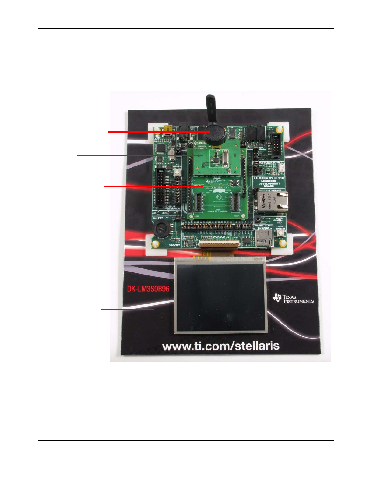
Stellaris® LM3S9B96 Development Kit User’s Manual
EM2 expansion board
EM module
Antenna for EM module
DK-LM3S9B96 board
4. Use a slight pressure to seat the EM module firmly on the EM2 expansion board. See
Figure G-6 on page 73 for fully assembled DK-LM3S9B96 board with EM2 expansion board
and wireless EM module.
Figure G-6. Fully Assembled DK-LM3S9B96 Board with EM2 Expansion Board and Wireless EM
Module
Follow these same steps for installing a second module into the secondary EM header location
which will be oriented 180 degrees from the primary EM header location.
NOTE: The secondary EM header should on ly be used whe n two EM modules are in stalled in the
system or when specifically indicated in the EM module’s README First document.
September 5, 2010 73
Page 74
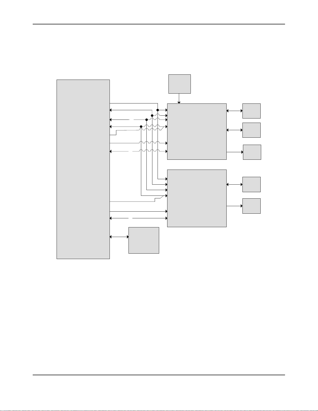
Hardware Description
EPI
Connector
UART1
MOD1 GP IO
MOD2 GP IO
MO D1 SHUTDOW N
MO D2 SHUTDOW N
SPI
MOD1 SPI_CS
MOD2 SPI_CS
MOD_I2C
AD_I2C
+3.3 V
CAT24C01
EEPROM
32 KHZ
OSC
/4
/4
/4
SDIO
Header
I2S
Audio
Header
Analog
Audio
Header
I2S
Audio
Header
Analog
Audio
Header
+3.3 V
I2C
UART
SPI
SHUT
DOWN
GPIO
+3.3 V
I2C
UART
SPI
SHUT
DOWN
GPIO
SECONDARY
EM
HEADER
(MOD2)
PRIMARY
EM
HEADER
(MOD1)
The block diagram for the EM2 expansion board is shown in Figure G-7.
Figure G-7. EM2 Expansion Board Block Diagram
Primary EM Header
74 September 5, 2010
The primary EM header should always be used when only one EM module is installed unless
otherwise indicated in the README First document for the EM module you are installing.
The primary EM header connects three buses to the EPI connector that are also shared with the
secondary EM header. These buses are I
2
C, UART1, and SPI.
NOTE: The primary and secondary EM headers have a unique SPI chip select signal, but share
the data and clock signals.
The primary EM header contains four GPIO connections to the EPI connector. These GPIOs can
be used as inputs or outputs depending upon th e EM module installed. In addition, four unique
GPIOs are provided to each EM header.
Page 75

The primary EM header contains one GPIO connection used to shut down and/or reset the EM
module. The actual function depends on the EM module installed. The MODx_nSHUTD signal is
pulled up to 3.3 V on the EM2 adapter. Each header has its own MODx_nSHUTD signal.
The primary EM header contains additional features not found on the secondary EM header
including a 32-KHz oscillator input and a header for a 4-bit SDIO module. These features are not
currently used by the EM modules available today but are available for future expansion.
Secondary EM Header
The secondary EM header should only be u sed wh en two EM m odu les are installed in the system
or when specifically indicated in the EM module’s README First document.
CAT24C01 EEPROM
The EM2 board contains a 1-Kbit I2C EEPROM which connects to an I2C bus separate from the
one connected to the EM headers. This EEPROM contains data that is used by the software
drivers to auto detect that the EM2 expansion board is installed in the system. The EEPROM is
normally write-protected. To make the EEPROM writeable, install a jumper between pins 2 and 3
of JPS1.
I2S Header
The primary EM header and the secondary EM header ea ch contain co nnections to separa te 6-pin
2
I
S headers J2 and J4 respectively. These headers connect to the EM modules only and are not
connected to the EPI header which connects to the DK-LM3S9B9 6. See th e EM mo d ule’s
documentation for more information on the functionality of this header.
Stellaris® LM3S9B96 Development Kit User’s Manual
Analog Audio Header
The primary EM header and the secondary EM header ea ch contain co nnections to separa te 4-pin
analog audio headers J3 and J5 respectively. These headers connect to the EM modules only and
are not connected to the EPI header which connects to the DK-LM3S9B96. See the EM module’s
documentation for more information on the functionality of this header.
SDIO Header
The primary EM header contains a connection to 8-pin SDIO header J1. This header connects to
the EM modules only and is not connected to the EPI header which con nects to the
DK-LM3S9B96. See the EM module’s documentation for more information on the functionality of
this header.
EPI Signal Descriptions
Figure G-1 provides the EPI module's signal descriptions.
Table G-1. EPI Signal Descriptions
LM3S9B96 Function Port EM2 Signal Direction Description
PE1 PE1 SPI_CS1 Out SPI Ch ip Select for Primary EM Module
PJ4 PJ4 SPI_CS2 Out SPI Chip Select for Secondary EM Module
SSI1CLK PH4 SPI_CLK Out SPI Clock
SSI1Rx PF4 SPI_MISO In SPI Receive
September 5, 2010 75
Page 76

Table G-1. EPI Signal Descriptions (Continued)
LM3S9B96 Function Port EM2 Signal Direction Description
SSI1TX PF5 SPI_MOSI Out SPI Transmit
U1RX PC6 MOD_UART_TX In Modulator UART TX, LM3S9B96 RX
U1TX PC7 MOD_UART_RX Out Modulator UART RX, LM3S9B96 TX
U1RTS PJ6 MOD_UART_CTS Out Modulator UART CTS, LM3S9B96 RTS
U1CTS PJ3 MOD_UART_RTS In Modulator UART RTS, LM3S9B96 CTS
I2C1SCL PJ0 MOD_I2C_SCL Out I
I2C1SDA PJ1 MOD_I2C_SDA I/O I
I2C0SCL PB2 AD_I2C_SCL0 Out I
I2C0SDA PB3 AD_I2C_SDA0 I/O I
PC4 PC4 MOD1_nSHUTD Out Shutdown/Reset Signal for Primary EM Module
PH5 PH5 MOD2_nSHUTD Out Shutdown/Reset Signal for Secondary EM Module
PH0 PH0 MOD1_GPIO0 I/O GPIO for Primary EM Module
PH1 PH1 MOD1_GPIO1 I/O GPIO for Primary EM Module
2
C Bus to EM Modules
2
C Bus to EM Modules
2
C Bus to Auto Discovery EEPROM
2
C Bus to Auto Discovery EEPROM
PH2 PH2 MOD1_GPIO2 I/O GPIO for Primary EM Module
PH3 PH3 MOD1_GPIO3 I/O GPIO for Primary EM Module
PG0 PG0 MOD2_GPIO0 I/O GPIO for Secondary EM Module
PG1 PG1 MOD2_GPIO1 I/O GPIO for Secondary EM Module
PG7 PG7 MOD2_GPIO2 I/O GPIO for Secondary EM Module
PJ2 PJ2 MOD2_GPIO3 I/O GPIO for Secondary EM Module
76 September 5, 2010
Page 77
Stellaris® LM3S9B96 Development Kit User’s Manual
Top
Bottom
Component Locations
Figure G-8 shows the details of the component locations.
Figure G-8. Component Placement Plot for Top and Bottom
Schematics
This section shows the schematics for the EM2 expansion board:
EM2 Expansion Board on page 78
September 5, 2010 77
Page 78
5
5
4
4
3
3
2
2
1
1
D D
C C
B B
A A
Primary EM header
Secondary EM header
Stellaris LM3S9B96 EPI header
32KHz Clock
INSTALL RESISTOR R7 WHEN 2nd
MODULE NEEDS SLOW CLK.
I2C chip to enable adapterboard auto discovery.
32KHz clock for BT boards
MOD1_SDIO_D0
MOD_UART_CTS
MOD1_SDIO_D1
MOD_SLOWCLK
MOD1_SDIO_D2
MOD1_SDIO_D3
MOD_UART_RX
MOD_UART_TX
MOD1_GPIO0
MOD_I2C_SDA
MOD1_GPIO1
MOD_I2C_SCL
MOD1_SDIO_CLK
SPI_CLK
MOD1_SDIO_CMD
SPI_MOSI
SPI_MISO
MOD1_AUD_DATA_IN
MOD1_AUD_FSYNC
MOD1_GPIO2
MOD1_nSHUTD
MOD1_AUD_CLK
MOD1_GPIO3
MOD1_nSHUTD
MOD1_AUD_ANA_L
MOD1_AUD_ANA_R
MOD1_AUD_DATA_OUT
MOD_UART_RTS
SPI_CS1
MOD1_AUD_DATA_OUT
MOD1_AUD_DATA_IN
MOD1_AUD_FSYNC
MOD1_AUD_CLK
MOD1_AUD_ANA_R
MOD1_AUD_ANA_L
MOD_UART_CTS
MOD2_AUD_ANA_R
MOD2_AUD_ANA_L
MOD_UART_RX
MOD_UART_TX
MOD_UART_RTS
MOD2_GPIO0 MOD2_AUD_DATA_IN
MOD2_AUD_FSYNC
MOD2_GPIO2
MOD2_nSHUTD
MOD2_AUD_CLK
MOD2_GPIO3
MOD_I2C_SDA
MOD2_nSHUTD
MOD2_GPIO1
MOD2_AUD_ANA_L
MOD2_AUD_DATA_OUT
MOD_I2C_SCL
MOD2_AUD_DATA_OUT
SPI_CS2
MOD2_AUD_ANA_R
SPI_CLK
MOD2_AUD_DATA_IN
MOD2_AUD_FSYNC
MOD2_AUD_CLK
SPI_MOSI
SPI_MISO
MOD1_SDIO_CMD
MOD1_SDIO_CLK
MOD1_SDIO_D3
MOD1_SDIO_D2
MOD1_SDIO_D1
MOD1_SDIO_D0
EPI13
EPI14
EPI16
EPI30
EPI17
EPI06
EPI01
EPI00
EPI10
EPI07
EPI04
EPI05
EPI31
EPI15
EPI12
EPI18
EPI09
EPI02
SPI_CS1
SPI_CLK
MOD1_GPIO0
MOD_I2C_SDA
MOD1_GPIO1
MOD1_GPIO2
MOD1_GPIO3
MOD_UART_CTS
MOD2_GPIO0
MOD2_GPIO1
SPI_MISO
SPI_MOSI
MOD2_GPIO2
MOD2_GPIO3
MOD1_nSHUTD
EPI19
EPI28
MOD_UART_RTS
MOD2_nSHUTD
MOD_UART_TX
MOD_UART_RX SEC_MOD_SCLK
WP_I2C
AD_I2C_SDA0
AD_I2C_SCL0
MOD_SLOWCLK
SEC_MOD_SCLK
SPI_CS2
EPI11
PB2
PB3
MOD_I2C_SCL
AD_I2C_SCL0
AD_I2C_SDA0
PB2
PB3
+3.3V
+3.3V
+3.3V
+3.3V
+3.3V
+3.3V
+3.3V
+3.3V
+3.3V
+3.3V
+3.3V
Title
Size Document Number Rev
Date: Sheet
of
DK-LM3S9B96_EM2
DK-LM3S9B96_EM2DK-LM3S9B96_EM2
DK-LM3S9B96_EM2
C
LM3S9B96 EM2 Adapter
LM3S9B96 EM2 AdapterLM3S9B96 EM2 Adapter
LM3S9B96 EM2 Adapter
B
11Monday, July 12, 2010
Title
Size Document Number Rev
Date: Sheet
of
DK-LM3S9B96_EM2
DK-LM3S9B96_EM2DK-LM3S9B96_EM2
DK-LM3S9B96_EM2
C
LM3S9B96 EM2 Adapter
LM3S9B96 EM2 AdapterLM3S9B96 EM2 Adapter
LM3S9B96 EM2 Adapter
B
11Monday, July 12, 2010
Title
Size Document Number Rev
Date: Sheet
of
DK-LM3S9B96_EM2
DK-LM3S9B96_EM2DK-LM3S9B96_EM2
DK-LM3S9B96_EM2
C
LM3S9B96 EM2 Adapter
LM3S9B96 EM2 AdapterLM3S9B96 EM2 Adapter
LM3S9B96 EM2 Adapter
B
11Monday, July 12, 2010
R15
2.7K
R15
2.7K
C4
1uFC41uF
JPS1
I2C_WP
JPS1
I2C_WP
1
3
2
J4
Header_1x6_100_430L
RFMOD2_I2S
J4
Header_1x6_100_430L
RFMOD2_I2S
1
2
3
4
5
6
J6
RECT_DF12A-50DS
LM3S9B96 EPI Header
J6
RECT_DF12A-50DS
LM3S9B96 EPI Header
1
2
3
4
5
6
7
8
9
10
11
12
13
14
15
16
17
18
19
20
21
22
23
24
25
50
49
48
47
46
45
44
43
42
41
40
39
38
37
36
35
34
33
32
31
30
29
28
27
26
R7 0
DNI
R7 0
DNI
R8 0R8 0
CC-P2CC-P1
MOD2
HPA_MB_MODULE_ASSY_RF
RF_MODULE-PORT_1A
TFM-110-02-S-D-K-A
TFM-110-02-S-D-K-A
CC-P2CC-P1
MOD2
HPA_MB_MODULE_ASSY_RF
RF_MODULE-PORT_1A
TFM-110-02-S-D-K-A
TFM-110-02-S-D-K-A
B7
B7
B8
B8
B9
B9
B10
B10
B11
B11
B12
B12
B13
B13
B14
B14
B15
B15
B16
B16
B17
B17
B18
B18
B19
B19
B20
B20
B1
B1
B2
B2
B3
B3
B4
B4
B5
B5
B6
B6
D1
D1
D2
D2
D3
D3
D4
D4
D5
D5
D6
D6
D7
D7
D8
D8
D9
D9
D10
D10
D11
D11
D12
D12
D13
D13
D14
D14
D15
D15
D16
D16
D17
D17
D18
D18
D19
D19
D20
D20
R13
2.7K
R13
2.7K
R227R2
27
1
2
3
4
5
6
7
89
10
11
12
13
14
15
16
R14
2.7K
R14
2.7K
U2
CAT24C01
U2
CAT24C01
A0
1
A1
2
A2
3
VSS4SDA
5
SCL
6
WP
7
VCC
8
J1
Header_1x8_100_430L
RFMOD1_SDIO
J1
Header_1x8_100_430L
RFMOD1_SDIO
1
2
3
4
5
6
7
8
R6
100KR6100K
XJ1
Shunt_100
XJ1
Shunt_100
R11
10K
R11
10K
C2
10000pF
DNI
C2
10000pF
DNI
C3
10nFC310nF
C5
1uFC51uF
J2
Header_1x6_100_430L
RFMOD1_I2S
J2
Header_1x6_100_430L
RFMOD1_I2S
1
2
3
4
5
6
R127R1
27
1
2
3
4
5
6
7
89
10
11
12
13
14
15
16
CC-P2CC-P1
MOD1
HPA_MB_MODULE_ASSY_RF
RF_MODULE-PORT_1A
TFM-110-02-S-D-K-A
TFM-110-02-S-D-K-A
CC-P2CC-P1
MOD1
HPA_MB_MODULE_ASSY_RF
RF_MODULE-PORT_1A
TFM-110-02-S-D-K-A
TFM-110-02-S-D-K-A
B7
B7
B8
B8
B9
B9
B10
B10
B11
B11
B12
B12
B13
B13
B14
B14
B15
B15
B16
B16
B17
B17
B18
B18
B19
B19
B20
B20
B1
B1
B2
B2
B3
B3
B4
B4
B5
B5
B6
B6
D1
D1
D2
D2
D3
D3
D4
D4
D5
D5
D6
D6
D7
D7
D8
D8
D9
D9
D10
D10
D11
D11
D12
D12
D13
D13
D14
D14
D15
D15
D16
D16
D17
D17
D18
D18
D19
D19
D20
D20
R327R3
27
1
2
3
4
5
6
7
89
10
11
12
13
14
15
16
J3
Header_1x4_100_430L
RFMOD1_ANALOG
J3
Header_1x4_100_430L
RFMOD1_ANALOG
1
2
3
4
R5
100KR5100K
R12
2.7K
R12
2.7K
OSC1
MC_32.768kHz
OSC1
MC_32.768kHz
VCC
4
OUT
1
GND2EN
3
J5
Header_1x4_100_430L
RFMOD2_ANALOG
J5
Header_1x4_100_430L
RFMOD2_ANALOG
1
2
3
4
EM2 Expansion Board
Page 79

APPENDIX H
References
In addition to this document, the following references are included on the Stellaris DK-LM3S9B96
Development Kit Documentation and Software CD and are also available for download at
www.ti.com/stellaris
Stellaris LM3S9B96 Microcontroller Data Sheet
Kitron ix LCD Data Sheet
StellarisWare Driver Library
StellarisWare Driver Library User’s Manual, publication number SW-DRL-UG
Additional references include:
FT2232D Dual USB/UART FIFO IC Data sheet, version 0.91, 2006, Future Technology
Devices International Ltd.
Texas Instruments TLV320AIC23BPM Audio CODEC Data Sheet
Information on development tool being used:
– RealView MDK web site, www.keil.com/arm/rvmdkkit.asp
– IAR Embedded Workbench web site, www.iar.com
– Code Sourcery GCC development tools web site,
www.codesourcery.com/gnu_toolchains/arm
:
– Code Red Technologies development tools web site, www.code-red-tech.com
– Texas Instruments’ Code Composer Studio™ IDE web site, www.ti.com/ccs
September 5, 2010 79
Page 80

80 September 5, 2010
Page 81

IMPORTANT NOTICE
Texas Instruments Incorporated and its subsidiaries (TI) reserve the right to make corrections, modifications, enhancements, improvements,
and other changes to its products and services at any time and to discontinue any product or service without notice. Customers should
obtain the latest relevant information before placing orders and should verify that such information is current and complete. All products are
sold subject to TI’s terms and conditions of sale supplied at the time of order acknowledgment.
TI warrants performance of its hardware products to the specifications applicable at the time of sale in accordance with TI’s standard
warranty. Testing and other quality control techniques are used to the extent TI deems necessary to support this warranty. Except where
mandated by government requirements, testing of all parameters of each product is not necessarily performed.
TI assumes no liability for applications assistance or customer product design. Customers are responsible for their products and
applications using TI components. To minimize the risks associated with customer products and applications, customers should provide
adequate design and operating safeguards.
TI does not warrant or represent that any license, either express or implied, is granted under any TI patent right, copyright, mask work right,
or other TI intellectual property right relating to any combination, machine, or process in which TI products or services are used. Information
published by TI regarding third-party products or services does not constitute a license from TI to use such products or services or a
warranty or endorsement thereof. Use of such information may require a license from a third party under the patents or other intellectual
property of the third party, or a license from TI under the patents or other intellectual property of TI.
Reproduction of TI information in TI data books or data sheets is permissible only if reproduction is without alteration and is accompanied
by all associated warranties, conditions, limitations, and notices. Reproduction of this information with alteration is an unfair and deceptive
business practice. TI is not responsible or liable for such altered documentation. Information of third parties may be subject to additional
restrictions.
Resale of TI products or services with statements different from or beyond the parameters stated by TI for that product or service voids all
express and any implied warranties for the associated TI product or service and is an unfair and deceptive business practice. TI is not
responsible or liable for any such statements.
TI products are not authorized for use in safety-critical applications (such as life support) where a failure of the TI product would reasonably
be expected to cause severe personal injury or death, unless officers of the parties have executed an agreement specifically governing
such use. Buyers represent that they have all necessary expertise in the safety and regulatory ramifications of their applications, and
acknowledge and agree that they are solely responsible for all legal, regulatory and safety-related requirements concerning their products
and any use of TI products in such safety-critical applications, notwithstanding any applications-related information or support that may be
provided by TI. Further, Buyers must fully indemnify TI and its representatives against any damages arising out of the use of TI products in
such safety-critical applications.
TI products are neither designed nor intended for use in military/aerospace applications or environments unless the TI products are
specifically designated by TI as military-grade or "enhanced plastic." Only products designated by TI as military-grade meet military
specifications. Buyers acknowledge and agree that any such use of TI products which TI has not designated as military-grade is solely at
the Buyer's risk, and that they are solely responsible for compliance with all legal and regulatory requirements in connection with such use.
TI products are neither designed nor intended for use in automotive applications or environments unless the specific TI products are
designated by TI as compliant with ISO/TS 16949 requirements. Buyers acknowledge and agree that, if they use any non-designated
products in automotive applications, TI will not be responsible for any failure to meet such requirements.
Following are URLs where you can obtain information on other Texas Instruments products and application solutions:
Products Applications
Audio www.ti.com/audio Communications and Telecom www.ti.com/communications
Amplifiers amplifier.ti.com Computers and Peripherals www.ti.com/computers
Data Converters dataconverter.ti.com Consumer Electronics www.ti.com/consumer-apps
DLP® Products www.dlp.com Energy and Lighting www.ti.com/energy
DSP dsp.ti.com Industrial www.ti.com/industrial
Clocks and Timers www.ti.com/clocks Medical www.ti.com/medical
Interface interface.ti.com Security www.ti.com/security
Logic logic.ti.com Space, Avionics and Defense www.ti.com/space-avionics-defense
Power Mgmt power.ti.com Transportation and www.ti.com/automotive
Microcontrollers microcontroller.ti.com Video and Imaging www.ti.com/video
RFID www.ti-rfid.com Wireless www.ti.com/wireless-apps
RF/IF and ZigBee® Solutions www.ti.com/lprf
TI E2E Community Home Page e2e.ti.com
Automotive
Mailing Address: Texas Instruments, Post Office Box 655303, Dallas, Texas 75265
Copyright © 2011, Texas Instruments Incorporated
 Loading...