

Page 1

TEXAS INSTRUMENTS-PRODUCTION DATA
Stellaris® LM3S1332 Microcontroller
DATA SHEET
DS-LM3S1332-7393
Copyright © 2007-2010 Texas Instruments
Incorporated
Page 2

Copyright
Copyright ©2007-2010 Texas Instruments Incorporated All rights reserved. Stellaris and StellarisWare are registered trademarks of Texas Instruments
Incorporated. ARM and Thumb are registered trademarks and Cortex is a trademark of ARM Limited. Other names and brands may be claimed as the
property of others.
PRODUCTION DATA information is current as of publication date. Products conform to specications per the terms of Texas Instruments standard
warranty. Production processing does not necessarily include testing of all parameters.
Please be aware that an important notice concerning availability, standard warranty, and use in critical applications of Texas Instruments semiconductor
products and disclaimers thereto appears at the end of this data sheet.
Texas Instruments Incorporated
108 Wild Basin, Suite 350
Austin, TX 78746
http://www.ti.com/stellaris
http://www-k.ext.ti.com/sc/technical-support/product-information-centers.htm
Texas Instruments-Production Data
June 23, 20102
Page 3

Stellaris® LM3S1332 Microcontroller
Table of Contents
Revision History ............................................................................................................................. 17
About This Document .................................................................................................................... 21
Audience .............................................................................................................................................. 21
About This Manual ................................................................................................................................ 21
Related Documents ............................................................................................................................... 21
Documentation Conventions .................................................................................................................. 22
1 Architectural Overview .......................................................................................... 24
1.1 Product Features .......................................................................................................... 24
1.2 Target Applications ........................................................................................................ 30
1.3 High-Level Block Diagram ............................................................................................. 31
1.4 Functional Overview ...................................................................................................... 33
1.4.1 ARM Cortex™-M3 ......................................................................................................... 33
1.4.2 Motor Control Peripherals .............................................................................................. 33
1.4.3 Analog Peripherals ........................................................................................................ 34
1.4.4 Serial Communications Peripherals ................................................................................ 35
1.4.5 System Peripherals ....................................................................................................... 35
1.4.6 Memory Peripherals ...................................................................................................... 36
1.4.7 Additional Features ....................................................................................................... 37
1.4.8 Hardware Details .......................................................................................................... 37
2 ARM Cortex-M3 Processor Core ........................................................................... 39
2.1 Block Diagram .............................................................................................................. 40
2.2 Functional Description ................................................................................................... 40
2.2.1 Serial Wire and JTAG Debug ......................................................................................... 40
2.2.2 Embedded Trace Macrocell (ETM) ................................................................................. 41
2.2.3 Trace Port Interface Unit (TPIU) ..................................................................................... 41
2.2.4 ROM Table ................................................................................................................... 41
2.2.5 Memory Protection Unit (MPU) ....................................................................................... 41
2.2.6 Nested Vectored Interrupt Controller (NVIC) .................................................................... 41
3 Memory Map ........................................................................................................... 45
4 Interrupts ................................................................................................................. 47
5 JTAG Interface ........................................................................................................ 50
5.1 Block Diagram .............................................................................................................. 51
5.2 Functional Description ................................................................................................... 51
5.2.1 JTAG Interface Pins ...................................................................................................... 51
5.2.2 JTAG TAP Controller ..................................................................................................... 53
5.2.3 Shift Registers .............................................................................................................. 54
5.2.4 Operational Considerations ............................................................................................ 54
5.3 Initialization and Configuration ....................................................................................... 57
5.4 Register Descriptions .................................................................................................... 57
5.4.1 Instruction Register (IR) ................................................................................................. 57
5.4.2 Data Registers .............................................................................................................. 59
6 System Control ....................................................................................................... 62
6.1 Functional Description ................................................................................................... 62
6.1.1 Device Identification ...................................................................................................... 62
Texas Instruments-Production Data
3June 23, 2010
Page 4

Table of Contents
6.1.2 Reset Control ................................................................................................................ 62
6.1.3 Power Control ............................................................................................................... 65
6.1.4 Clock Control ................................................................................................................ 66
6.1.5 System Control ............................................................................................................. 71
6.2 Initialization and Configuration ....................................................................................... 72
6.3 Register Map ................................................................................................................ 73
6.4 Register Descriptions .................................................................................................... 74
7 Hibernation Module .............................................................................................. 124
7.1 Block Diagram ............................................................................................................ 125
7.2 Functional Description ................................................................................................. 125
7.2.1 Register Access Timing ............................................................................................... 125
7.2.2 Clock Source .............................................................................................................. 126
7.2.3 Battery Management ................................................................................................... 127
7.2.4 Real-Time Clock .......................................................................................................... 127
7.2.5 Non-Volatile Memory ................................................................................................... 128
7.2.6 Power Control ............................................................................................................. 128
7.2.7 Initiating Hibernate ...................................................................................................... 128
7.2.8 Interrupts and Status ................................................................................................... 129
7.3 Initialization and Configuration ..................................................................................... 129
7.3.1 Initialization ................................................................................................................. 129
7.3.2 RTC Match Functionality (No Hibernation) .................................................................... 129
7.3.3 RTC Match/Wake-Up from Hibernation ......................................................................... 130
7.3.4 External Wake-Up from Hibernation .............................................................................. 130
7.3.5 RTC/External Wake-Up from Hibernation ...................................................................... 130
7.4 Register Map .............................................................................................................. 130
7.5 Register Descriptions .................................................................................................. 131
8 Internal Memory ................................................................................................... 144
8.1 Block Diagram ............................................................................................................ 144
8.2 Functional Description ................................................................................................. 144
8.2.1 SRAM Memory ............................................................................................................ 144
8.2.2 Flash Memory ............................................................................................................. 145
8.3 Flash Memory Initialization and Configuration ............................................................... 146
8.3.1 Flash Programming ..................................................................................................... 146
8.3.2 Nonvolatile Register Programming ............................................................................... 147
8.4 Register Map .............................................................................................................. 148
8.5 Flash Register Descriptions (Flash Control Offset) ......................................................... 148
8.6 Flash Register Descriptions (System Control Offset) ...................................................... 156
9 General-Purpose Input/Outputs (GPIOs) ........................................................... 169
9.1 Functional Description ................................................................................................. 169
9.1.1 Data Control ............................................................................................................... 170
9.1.2 Interrupt Control .......................................................................................................... 171
9.1.3 Mode Control .............................................................................................................. 172
9.1.4 Commit Control ........................................................................................................... 172
9.1.5 Pad Control ................................................................................................................. 172
9.1.6 Identification ............................................................................................................... 173
9.2 Initialization and Configuration ..................................................................................... 173
9.3 Register Map .............................................................................................................. 174
9.4 Register Descriptions .................................................................................................. 176
Texas Instruments-Production Data
June 23, 20104
Page 5

Stellaris® LM3S1332 Microcontroller
10 General-Purpose Timers ...................................................................................... 211
10.1 Block Diagram ............................................................................................................ 212
10.2 Functional Description ................................................................................................. 213
10.2.1 GPTM Reset Conditions .............................................................................................. 213
10.2.2 32-Bit Timer Operating Modes ...................................................................................... 213
10.2.3 16-Bit Timer Operating Modes ...................................................................................... 214
10.3 Initialization and Configuration ..................................................................................... 218
10.3.1 32-Bit One-Shot/Periodic Timer Mode ........................................................................... 218
10.3.2 32-Bit Real-Time Clock (RTC) Mode ............................................................................. 219
10.3.3 16-Bit One-Shot/Periodic Timer Mode ........................................................................... 219
10.3.4 16-Bit Input Edge Count Mode ..................................................................................... 220
10.3.5 16-Bit Input Edge Timing Mode .................................................................................... 220
10.3.6 16-Bit PWM Mode ....................................................................................................... 221
10.4 Register Map .............................................................................................................. 221
10.5 Register Descriptions .................................................................................................. 222
11 Watchdog Timer ................................................................................................... 247
11.1 Block Diagram ............................................................................................................ 248
11.2 Functional Description ................................................................................................. 248
11.3 Initialization and Configuration ..................................................................................... 249
11.4 Register Map .............................................................................................................. 249
11.5 Register Descriptions .................................................................................................. 250
12 Analog-to-Digital Converter (ADC) ..................................................................... 271
12.1 Block Diagram ............................................................................................................ 271
12.2 Functional Description ................................................................................................. 272
12.2.1 Sample Sequencers .................................................................................................... 272
12.2.2 Module Control ............................................................................................................ 273
12.2.3 Hardware Sample Averaging Circuit ............................................................................. 274
12.2.4 Analog-to-Digital Converter .......................................................................................... 274
12.2.5 Differential Sampling ................................................................................................... 274
12.2.6 Test Modes ................................................................................................................. 276
12.2.7 Internal Temperature Sensor ........................................................................................ 277
12.3 Initialization and Configuration ..................................................................................... 277
12.3.1 Module Initialization ..................................................................................................... 277
12.3.2 Sample Sequencer Configuration ................................................................................. 278
12.4 Register Map .............................................................................................................. 278
12.5 Register Descriptions .................................................................................................. 279
13 Universal Asynchronous Receivers/Transmitters (UARTs) ............................. 307
13.1 Block Diagram ............................................................................................................ 308
13.2 Functional Description ................................................................................................. 308
13.2.1 Transmit/Receive Logic ............................................................................................... 308
13.2.2 Baud-Rate Generation ................................................................................................. 309
13.2.3 Data Transmission ...................................................................................................... 310
13.2.4 Serial IR (SIR) ............................................................................................................. 310
13.2.5 FIFO Operation ........................................................................................................... 311
13.2.6 Interrupts .................................................................................................................... 311
13.2.7 Loopback Operation .................................................................................................... 312
13.2.8 IrDA SIR block ............................................................................................................ 312
13.3 Initialization and Configuration ..................................................................................... 312
Texas Instruments-Production Data
5June 23, 2010
Page 6

Table of Contents
13.4 Register Map .............................................................................................................. 313
13.5 Register Descriptions .................................................................................................. 314
14 Synchronous Serial Interface (SSI) .................................................................... 348
14.1 Block Diagram ............................................................................................................ 348
14.2 Functional Description ................................................................................................. 348
14.2.1 Bit Rate Generation ..................................................................................................... 349
14.2.2 FIFO Operation ........................................................................................................... 349
14.2.3 Interrupts .................................................................................................................... 349
14.2.4 Frame Formats ........................................................................................................... 350
14.3 Initialization and Configuration ..................................................................................... 357
14.4 Register Map .............................................................................................................. 358
14.5 Register Descriptions .................................................................................................. 359
15 Analog Comparators ............................................................................................ 385
15.1 Block Diagram ............................................................................................................ 386
15.2 Functional Description ................................................................................................. 386
15.2.1 Internal Reference Programming .................................................................................. 387
15.3 Initialization and Configuration ..................................................................................... 388
15.4 Register Map .............................................................................................................. 388
15.5 Register Descriptions .................................................................................................. 389
16 Pin Diagram .......................................................................................................... 397
17 Signal Tables ........................................................................................................ 399
17.1 100-Pin LQFP Package Pin Tables ............................................................................... 399
17.2 108-Pin BGA Package Pin Tables ................................................................................ 410
17.3 Connections for Unused Signals ................................................................................... 422
18 Operating Characteristics ................................................................................... 424
19 Electrical Characteristics .................................................................................... 425
19.1 DC Characteristics ...................................................................................................... 425
19.1.1 Maximum Ratings ....................................................................................................... 425
19.1.2 Recommended DC Operating Conditions ...................................................................... 425
19.1.3 On-Chip Low Drop-Out (LDO) Regulator Characteristics ................................................ 426
19.1.4 GPIO Module Characteristics ....................................................................................... 426
19.1.5 Power Specifications ................................................................................................... 426
19.1.6 Flash Memory Characteristics ...................................................................................... 428
19.1.7 Hibernation ................................................................................................................. 428
19.2 AC Characteristics ....................................................................................................... 428
19.2.1 Load Conditions .......................................................................................................... 428
19.2.2 Clocks ........................................................................................................................ 429
19.2.3 JTAG and Boundary Scan ............................................................................................ 430
19.2.4 Reset ......................................................................................................................... 432
19.2.5 Sleep Modes ............................................................................................................... 434
19.2.6 Hibernation Module ..................................................................................................... 434
19.2.7 General-Purpose I/O (GPIO) ........................................................................................ 435
19.2.8 Analog-to-Digital Converter .......................................................................................... 435
19.2.9 Synchronous Serial Interface (SSI) ............................................................................... 436
19.2.10 Analog Comparator ..................................................................................................... 438
A Serial Flash Loader .............................................................................................. 439
A.1 Serial Flash Loader ..................................................................................................... 439
Texas Instruments-Production Data
June 23, 20106
Page 7

Stellaris® LM3S1332 Microcontroller
A.2 Interfaces ................................................................................................................... 439
A.2.1 UART ......................................................................................................................... 439
A.2.2 SSI ............................................................................................................................. 439
A.3 Packet Handling .......................................................................................................... 440
A.3.1 Packet Format ............................................................................................................ 440
A.3.2 Sending Packets ......................................................................................................... 440
A.3.3 Receiving Packets ....................................................................................................... 440
A.4 Commands ................................................................................................................. 441
A.4.1 COMMAND_PING (0X20) ............................................................................................ 441
A.4.2 COMMAND_GET_STATUS (0x23) ............................................................................... 441
A.4.3 COMMAND_DOWNLOAD (0x21) ................................................................................. 441
A.4.4 COMMAND_SEND_DATA (0x24) ................................................................................. 442
A.4.5 COMMAND_RUN (0x22) ............................................................................................. 442
A.4.6 COMMAND_RESET (0x25) ......................................................................................... 442
B Register Quick Reference ................................................................................... 444
C Ordering and Contact Information ..................................................................... 457
C.1 Ordering Information .................................................................................................... 457
C.2 Part Markings .............................................................................................................. 457
C.3 Kits ............................................................................................................................. 458
C.4 Support Information ..................................................................................................... 458
D Package Information ............................................................................................ 459
Texas Instruments-Production Data
7June 23, 2010
Page 8

Table of Contents
List of Figures
Figure 1-1. Stellaris®LM3S1332 Microcontroller High-Level Block Diagram ............................. 32
Figure 2-1. CPU Block Diagram ............................................................................................. 40
Figure 2-2. TPIU Block Diagram ............................................................................................ 41
Figure 5-1. JTAG Module Block Diagram ................................................................................ 51
Figure 5-2. Test Access Port State Machine ........................................................................... 54
Figure 5-3. IDCODE Register Format ..................................................................................... 60
Figure 5-4. BYPASS Register Format .................................................................................... 60
Figure 5-5. Boundary Scan Register Format ........................................................................... 61
Figure 6-1. Basic RST Configuration ...................................................................................... 63
Figure 6-2. External Circuitry to Extend Power-On Reset ........................................................ 64
Figure 6-3. Reset Circuit Controlled by Switch ........................................................................ 64
Figure 6-4. Power Architecture .............................................................................................. 66
Figure 6-5. Main Clock Tree .................................................................................................. 68
Figure 7-1. Hibernation Module Block Diagram ..................................................................... 125
Figure 7-2. Clock Source Using Crystal ................................................................................ 126
Figure 7-3. Clock Source Using Dedicated Oscillator ............................................................. 127
Figure 8-1. Flash Block Diagram .......................................................................................... 144
Figure 9-1. GPIO Port Block Diagram ................................................................................... 170
Figure 9-2. GPIODATA Write Example ................................................................................. 171
Figure 9-3. GPIODATA Read Example ................................................................................. 171
Figure 10-1. GPTM Module Block Diagram ............................................................................ 212
Figure 10-2. 16-Bit Input Edge Count Mode Example .............................................................. 216
Figure 10-3. 16-Bit Input Edge Time Mode Example ............................................................... 217
Figure 10-4. 16-Bit PWM Mode Example ................................................................................ 218
Figure 11-1. WDT Module Block Diagram .............................................................................. 248
Figure 12-1. ADC Module Block Diagram ............................................................................... 272
Figure 12-2. Differential Sampling Range, V
Figure 12-3. Differential Sampling Range, V
Figure 12-4. Differential Sampling Range, V
Figure 12-5. Internal Temperature Sensor Characteristic ......................................................... 277
Figure 13-1. UART Module Block Diagram ............................................................................. 308
Figure 13-2. UART Character Frame ..................................................................................... 309
Figure 13-3. IrDA Data Modulation ......................................................................................... 311
Figure 14-1. SSI Module Block Diagram ................................................................................. 348
Figure 14-2. TI Synchronous Serial Frame Format (Single Transfer) ........................................ 351
Figure 14-3. TI Synchronous Serial Frame Format (Continuous Transfer) ................................ 351
Figure 14-4. Freescale SPI Format (Single Transfer) with SPO=0 and SPH=0 .......................... 352
Figure 14-5. Freescale SPI Format (Continuous Transfer) with SPO=0 and SPH=0 .................. 352
Figure 14-6. Freescale SPI Frame Format with SPO=0 and SPH=1 ......................................... 353
Figure 14-7. Freescale SPI Frame Format (Single Transfer) with SPO=1 and SPH=0 ............... 354
Figure 14-8. Freescale SPI Frame Format (Continuous Transfer) with SPO=1 and SPH=0 ........ 354
Figure 14-9. Freescale SPI Frame Format with SPO=1 and SPH=1 ......................................... 355
Figure 14-10. MICROWIRE Frame Format (Single Frame) ........................................................ 356
Figure 14-11. MICROWIRE Frame Format (Continuous Transfer) ............................................. 357
Figure 14-12. MICROWIRE Frame Format, SSIFss Input Setup and Hold Requirements ............ 357
IN_ODD
IN_ODD
IN_ODD
= 1.5 V ...................................................... 275
= 0.75 V .................................................... 276
= 2.25 V .................................................... 276
Texas Instruments-Production Data
June 23, 20108
Page 9

Stellaris® LM3S1332 Microcontroller
Figure 15-1. Analog Comparator Module Block Diagram ......................................................... 386
Figure 15-2. Structure of Comparator Unit .............................................................................. 387
Figure 15-3. Comparator Internal Reference Structure ............................................................ 387
Figure 16-1. 100-Pin LQFP Package Pin Diagram .................................................................. 397
Figure 16-2. 108-Ball BGA Package Pin Diagram (Top View) ................................................... 398
Figure 19-1. Load Conditions ................................................................................................ 429
Figure 19-2. JTAG Test Clock Input Timing ............................................................................. 431
Figure 19-3. JTAG Test Access Port (TAP) Timing .................................................................. 432
Figure 19-4. JTAG TRST Timing ............................................................................................ 432
Figure 19-5. External Reset Timing (RST) .............................................................................. 433
Figure 19-6. Power-On Reset Timing ..................................................................................... 433
Figure 19-7. Brown-Out Reset Timing .................................................................................... 433
Figure 19-8. Software Reset Timing ....................................................................................... 433
Figure 19-9. Watchdog Reset Timing ..................................................................................... 434
Figure 19-10. Hibernation Module Timing ................................................................................. 435
Figure 19-11. ADC Input Equivalency Diagram ......................................................................... 436
Figure 19-12. SSI Timing for TI Frame Format (FRF=01), Single Transfer Timing
Measurement .................................................................................................... 437
Figure 19-13. SSI Timing for MICROWIRE Frame Format (FRF=10), Single Transfer ................. 437
Figure 19-14. SSI Timing for SPI Frame Format (FRF=00), with SPH=1 ..................................... 438
Figure D-1. 100-Pin LQFP Package ...................................................................................... 459
Figure D-2. 108-Ball BGA Package ...................................................................................... 461
Texas Instruments-Production Data
9June 23, 2010
Page 10

Table of Contents
List of Tables
Table 1. Revision History .................................................................................................. 17
Table 2. Documentation Conventions ................................................................................ 22
Table 3-1. Memory Map ....................................................................................................... 45
Table 4-1. Exception Types .................................................................................................. 47
Table 4-2. Interrupts ............................................................................................................ 48
Table 5-1. JTAG Port Pins Reset State ................................................................................. 52
Table 5-2. JTAG Instruction Register Commands ................................................................... 57
Table 6-1. Clock Source Options .......................................................................................... 67
Table 6-2. Possible System Clock Frequencies Using the SYSDIV Field ................................. 69
Table 6-3. Examples of Possible System Clock Frequencies Using the SYSDIV2 Field ............ 69
Table 6-4. System Control Register Map ............................................................................... 73
Table 6-5. RCC2 Fields that Override RCC fields .................................................................. 88
Table 7-1. Hibernation Module Register Map ....................................................................... 130
Table 8-1. Flash Protection Policy Combinations ................................................................. 145
Table 8-2. User-Programmable Flash Memory Resident Registers ....................................... 147
Table 8-3. Flash Register Map ............................................................................................ 148
Table 9-1. GPIO Pad Configuration Examples ..................................................................... 173
Table 9-2. GPIO Interrupt Configuration Example ................................................................ 173
Table 9-3. GPIO Register Map ........................................................................................... 175
Table 10-1. Available CCP Pins ............................................................................................ 212
Table 10-2. 16-Bit Timer With Prescaler Configurations ......................................................... 215
Table 10-3. Timers Register Map .......................................................................................... 221
Table 11-1. Watchdog Timer Register Map ............................................................................ 249
Table 12-1. Samples and FIFO Depth of Sequencers ............................................................ 272
Table 12-2. Differential Sampling Pairs ................................................................................. 274
Table 12-3. ADC Register Map ............................................................................................. 278
Table 13-1. UART Register Map ........................................................................................... 313
Table 14-1. SSI Register Map .............................................................................................. 358
Table 15-1. Internal Reference Voltage and ACREFCTL Field Values ..................................... 387
Table 15-2. Analog Comparators Register Map ..................................................................... 389
Table 17-1. Signals by Pin Number ....................................................................................... 399
Table 17-2. Signals by Signal Name ..................................................................................... 403
Table 17-3. Signals by Function, Except for GPIO ................................................................. 406
Table 17-4. GPIO Pins and Alternate Functions ..................................................................... 409
Table 17-5. Signals by Pin Number ....................................................................................... 410
Table 17-6. Signals by Signal Name ..................................................................................... 415
Table 17-7. Signals by Function, Except for GPIO ................................................................. 418
Table 17-8. GPIO Pins and Alternate Functions ..................................................................... 421
Table 17-9. Connections for Unused Signals (100-pin LQFP) ................................................. 423
Table 17-10. Connections for Unused Signals, 108-pin BGA .................................................... 423
Table 18-1. Temperature Characteristics ............................................................................... 424
Table 18-2. Thermal Characteristics ..................................................................................... 424
Table 18-3. ESD Absolute Maximum Ratings ........................................................................ 424
Table 19-1. Maximum Ratings .............................................................................................. 425
Table 19-2. Recommended DC Operating Conditions ............................................................ 425
Table 19-3. LDO Regulator Characteristics ........................................................................... 426
Texas Instruments-Production Data
June 23, 201010
Page 11

Stellaris® LM3S1332 Microcontroller
Table 19-4. GPIO Module DC Characteristics ........................................................................ 426
Table 19-5. Detailed Power Specifications ............................................................................ 427
Table 19-6. Flash Memory Characteristics ............................................................................ 428
Table 19-7. Hibernation Module DC Characteristics ............................................................... 428
Table 19-8. Phase Locked Loop (PLL) Characteristics ........................................................... 429
Table 19-9. Actual PLL Frequency ........................................................................................ 429
Table 19-10. Clock Characteristics ......................................................................................... 429
Table 19-11. Crystal Characteristics ....................................................................................... 430
Table 19-12. System Clock Characteristics with ADC Operation ............................................... 430
Table 19-13. JTAG Characteristics ......................................................................................... 430
Table 19-14. Reset Characteristics ......................................................................................... 432
Table 19-15. Sleep Modes AC Characteristics ......................................................................... 434
Table 19-16. Hibernation Module AC Characteristics ............................................................... 434
Table 19-17. GPIO Characteristics ......................................................................................... 435
Table 19-18. ADC Characteristics ........................................................................................... 435
Table 19-19. ADC Module Internal Reference Characteristics .................................................. 436
Table 19-20. SSI Characteristics ............................................................................................ 436
Table 19-21. Analog Comparator Characteristics ..................................................................... 438
Table 19-22. Analog Comparator Voltage Reference Characteristics ........................................ 438
Table C-1. Part Ordering Information ................................................................................... 457
Texas Instruments-Production Data
11June 23, 2010
Page 12

Table of Contents
List of Registers
System Control .............................................................................................................................. 62
Register 1: Device Identification 0 (DID0), offset 0x000 ....................................................................... 75
Register 2: Brown-Out Reset Control (PBORCTL), offset 0x030 .......................................................... 77
Register 3: LDO Power Control (LDOPCTL), offset 0x034 ................................................................... 78
Register 4: Raw Interrupt Status (RIS), offset 0x050 ........................................................................... 79
Register 5: Interrupt Mask Control (IMC), offset 0x054 ........................................................................ 80
Register 6: Masked Interrupt Status and Clear (MISC), offset 0x058 .................................................... 81
Register 7: Reset Cause (RESC), offset 0x05C .................................................................................. 82
Register 8: Run-Mode Clock Configuration (RCC), offset 0x060 .......................................................... 83
Register 9: XTAL to PLL Translation (PLLCFG), offset 0x064 .............................................................. 87
Register 10: Run-Mode Clock Configuration 2 (RCC2), offset 0x070 ...................................................... 88
Register 11: Deep Sleep Clock Configuration (DSLPCLKCFG), offset 0x144 .......................................... 90
Register 12: Device Identification 1 (DID1), offset 0x004 ....................................................................... 91
Register 13: Device Capabilities 0 (DC0), offset 0x008 ......................................................................... 93
Register 14: Device Capabilities 1 (DC1), offset 0x010 ......................................................................... 94
Register 15: Device Capabilities 2 (DC2), offset 0x014 ......................................................................... 96
Register 16: Device Capabilities 3 (DC3), offset 0x018 ......................................................................... 98
Register 17: Device Capabilities 4 (DC4), offset 0x01C ....................................................................... 100
Register 18: Run Mode Clock Gating Control Register 0 (RCGC0), offset 0x100 ................................... 102
Register 19: Sleep Mode Clock Gating Control Register 0 (SCGC0), offset 0x110 ................................. 104
Register 20: Deep Sleep Mode Clock Gating Control Register 0 (DCGC0), offset 0x120 ....................... 106
Register 21: Run Mode Clock Gating Control Register 1 (RCGC1), offset 0x104 ................................... 108
Register 22: Sleep Mode Clock Gating Control Register 1 (SCGC1), offset 0x114 ................................. 110
Register 23: Deep Sleep Mode Clock Gating Control Register 1 (DCGC1), offset 0x124 ....................... 112
Register 24: Run Mode Clock Gating Control Register 2 (RCGC2), offset 0x108 ................................... 114
Register 25: Sleep Mode Clock Gating Control Register 2 (SCGC2), offset 0x118 ................................. 116
Register 26: Deep Sleep Mode Clock Gating Control Register 2 (DCGC2), offset 0x128 ....................... 118
Register 27: Software Reset Control 0 (SRCR0), offset 0x040 ............................................................. 120
Register 28: Software Reset Control 1 (SRCR1), offset 0x044 ............................................................. 121
Register 29: Software Reset Control 2 (SRCR2), offset 0x048 ............................................................. 123
Hibernation Module ..................................................................................................................... 124
Register 1: Hibernation RTC Counter (HIBRTCC), offset 0x000 ......................................................... 132
Register 2: Hibernation RTC Match 0 (HIBRTCM0), offset 0x004 ....................................................... 133
Register 3: Hibernation RTC Match 1 (HIBRTCM1), offset 0x008 ....................................................... 134
Register 4: Hibernation RTC Load (HIBRTCLD), offset 0x00C ........................................................... 135
Register 5: Hibernation Control (HIBCTL), offset 0x010 ..................................................................... 136
Register 6: Hibernation Interrupt Mask (HIBIM), offset 0x014 ............................................................. 138
Register 7: Hibernation Raw Interrupt Status (HIBRIS), offset 0x018 .................................................. 139
Register 8: Hibernation Masked Interrupt Status (HIBMIS), offset 0x01C ............................................ 140
Register 9: Hibernation Interrupt Clear (HIBIC), offset 0x020 ............................................................. 141
Register 10: Hibernation RTC Trim (HIBRTCT), offset 0x024 ............................................................... 142
Register 11: Hibernation Data (HIBDATA), offset 0x030-0x12C ............................................................ 143
Internal Memory ........................................................................................................................... 144
Register 1: Flash Memory Address (FMA), offset 0x000 .................................................................... 149
Register 2: Flash Memory Data (FMD), offset 0x004 ......................................................................... 150
Texas Instruments-Production Data
June 23, 201012
Page 13

Stellaris® LM3S1332 Microcontroller
Register 3: Flash Memory Control (FMC), offset 0x008 ..................................................................... 151
Register 4: Flash Controller Raw Interrupt Status (FCRIS), offset 0x00C ............................................ 153
Register 5: Flash Controller Interrupt Mask (FCIM), offset 0x010 ........................................................ 154
Register 6: Flash Controller Masked Interrupt Status and Clear (FCMISC), offset 0x014 ..................... 155
Register 7: USec Reload (USECRL), offset 0x140 ............................................................................ 157
Register 8: Flash Memory Protection Read Enable 0 (FMPRE0), offset 0x130 and 0x200 ................... 158
Register 9: Flash Memory Protection Program Enable 0 (FMPPE0), offset 0x134 and 0x400 ............... 159
Register 10: User Debug (USER_DBG), offset 0x1D0 ......................................................................... 160
Register 11: User Register 0 (USER_REG0), offset 0x1E0 .................................................................. 161
Register 12: User Register 1 (USER_REG1), offset 0x1E4 .................................................................. 162
Register 13: Flash Memory Protection Read Enable 1 (FMPRE1), offset 0x204 .................................... 163
Register 14: Flash Memory Protection Read Enable 2 (FMPRE2), offset 0x208 .................................... 164
Register 15: Flash Memory Protection Read Enable 3 (FMPRE3), offset 0x20C ................................... 165
Register 16: Flash Memory Protection Program Enable 1 (FMPPE1), offset 0x404 ............................... 166
Register 17: Flash Memory Protection Program Enable 2 (FMPPE2), offset 0x408 ............................... 167
Register 18: Flash Memory Protection Program Enable 3 (FMPPE3), offset 0x40C ............................... 168
General-Purpose Input/Outputs (GPIOs) ................................................................................... 169
Register 1: GPIO Data (GPIODATA), offset 0x000 ............................................................................ 177
Register 2: GPIO Direction (GPIODIR), offset 0x400 ......................................................................... 178
Register 3: GPIO Interrupt Sense (GPIOIS), offset 0x404 .................................................................. 179
Register 4: GPIO Interrupt Both Edges (GPIOIBE), offset 0x408 ........................................................ 180
Register 5: GPIO Interrupt Event (GPIOIEV), offset 0x40C ................................................................ 181
Register 6: GPIO Interrupt Mask (GPIOIM), offset 0x410 ................................................................... 182
Register 7: GPIO Raw Interrupt Status (GPIORIS), offset 0x414 ........................................................ 183
Register 8: GPIO Masked Interrupt Status (GPIOMIS), offset 0x418 ................................................... 184
Register 9: GPIO Interrupt Clear (GPIOICR), offset 0x41C ................................................................ 185
Register 10: GPIO Alternate Function Select (GPIOAFSEL), offset 0x420 ............................................ 186
Register 11: GPIO 2-mA Drive Select (GPIODR2R), offset 0x500 ........................................................ 188
Register 12: GPIO 4-mA Drive Select (GPIODR4R), offset 0x504 ........................................................ 189
Register 13: GPIO 8-mA Drive Select (GPIODR8R), offset 0x508 ........................................................ 190
Register 14: GPIO Open Drain Select (GPIOODR), offset 0x50C ......................................................... 191
Register 15: GPIO Pull-Up Select (GPIOPUR), offset 0x510 ................................................................ 192
Register 16: GPIO Pull-Down Select (GPIOPDR), offset 0x514 ........................................................... 193
Register 17: GPIO Slew Rate Control Select (GPIOSLR), offset 0x518 ................................................ 194
Register 18: GPIO Digital Enable (GPIODEN), offset 0x51C ................................................................ 195
Register 19: GPIO Lock (GPIOLOCK), offset 0x520 ............................................................................ 196
Register 20: GPIO Commit (GPIOCR), offset 0x524 ............................................................................ 197
Register 21: GPIO Peripheral Identification 4 (GPIOPeriphID4), offset 0xFD0 ....................................... 199
Register 22: GPIO Peripheral Identification 5 (GPIOPeriphID5), offset 0xFD4 ....................................... 200
Register 23: GPIO Peripheral Identification 6 (GPIOPeriphID6), offset 0xFD8 ....................................... 201
Register 24: GPIO Peripheral Identification 7 (GPIOPeriphID7), offset 0xFDC ...................................... 202
Register 25: GPIO Peripheral Identification 0 (GPIOPeriphID0), offset 0xFE0 ....................................... 203
Register 26: GPIO Peripheral Identification 1 (GPIOPeriphID1), offset 0xFE4 ....................................... 204
Register 27: GPIO Peripheral Identification 2 (GPIOPeriphID2), offset 0xFE8 ....................................... 205
Register 28: GPIO Peripheral Identification 3 (GPIOPeriphID3), offset 0xFEC ...................................... 206
Register 29: GPIO PrimeCell Identification 0 (GPIOPCellID0), offset 0xFF0 .......................................... 207
Register 30: GPIO PrimeCell Identification 1 (GPIOPCellID1), offset 0xFF4 .......................................... 208
Register 31: GPIO PrimeCell Identification 2 (GPIOPCellID2), offset 0xFF8 .......................................... 209
Texas Instruments-Production Data
13June 23, 2010
Page 14

Table of Contents
Register 32: GPIO PrimeCell Identification 3 (GPIOPCellID3), offset 0xFFC ......................................... 210
General-Purpose Timers ............................................................................................................. 211
Register 1: GPTM Configuration (GPTMCFG), offset 0x000 .............................................................. 223
Register 2: GPTM TimerA Mode (GPTMTAMR), offset 0x004 ............................................................ 224
Register 3: GPTM TimerB Mode (GPTMTBMR), offset 0x008 ............................................................ 226
Register 4: GPTM Control (GPTMCTL), offset 0x00C ........................................................................ 228
Register 5: GPTM Interrupt Mask (GPTMIMR), offset 0x018 .............................................................. 231
Register 6: GPTM Raw Interrupt Status (GPTMRIS), offset 0x01C ..................................................... 233
Register 7: GPTM Masked Interrupt Status (GPTMMIS), offset 0x020 ................................................ 234
Register 8: GPTM Interrupt Clear (GPTMICR), offset 0x024 .............................................................. 235
Register 9: GPTM TimerA Interval Load (GPTMTAILR), offset 0x028 ................................................. 237
Register 10: GPTM TimerB Interval Load (GPTMTBILR), offset 0x02C ................................................ 238
Register 11: GPTM TimerA Match (GPTMTAMATCHR), offset 0x030 ................................................... 239
Register 12: GPTM TimerB Match (GPTMTBMATCHR), offset 0x034 .................................................. 240
Register 13: GPTM TimerA Prescale (GPTMTAPR), offset 0x038 ........................................................ 241
Register 14: GPTM TimerB Prescale (GPTMTBPR), offset 0x03C ....................................................... 242
Register 15: GPTM TimerA Prescale Match (GPTMTAPMR), offset 0x040 ........................................... 243
Register 16: GPTM TimerB Prescale Match (GPTMTBPMR), offset 0x044 ........................................... 244
Register 17: GPTM TimerA (GPTMTAR), offset 0x048 ........................................................................ 245
Register 18: GPTM TimerB (GPTMTBR), offset 0x04C ....................................................................... 246
Watchdog Timer ........................................................................................................................... 247
Register 1: Watchdog Load (WDTLOAD), offset 0x000 ...................................................................... 251
Register 2: Watchdog Value (WDTVALUE), offset 0x004 ................................................................... 252
Register 3: Watchdog Control (WDTCTL), offset 0x008 ..................................................................... 253
Register 4: Watchdog Interrupt Clear (WDTICR), offset 0x00C .......................................................... 254
Register 5: Watchdog Raw Interrupt Status (WDTRIS), offset 0x010 .................................................. 255
Register 6: Watchdog Masked Interrupt Status (WDTMIS), offset 0x014 ............................................. 256
Register 7: Watchdog Test (WDTTEST), offset 0x418 ....................................................................... 257
Register 8: Watchdog Lock (WDTLOCK), offset 0xC00 ..................................................................... 258
Register 9: Watchdog Peripheral Identification 4 (WDTPeriphID4), offset 0xFD0 ................................. 259
Register 10: Watchdog Peripheral Identification 5 (WDTPeriphID5), offset 0xFD4 ................................. 260
Register 11: Watchdog Peripheral Identification 6 (WDTPeriphID6), offset 0xFD8 ................................. 261
Register 12: Watchdog Peripheral Identification 7 (WDTPeriphID7), offset 0xFDC ................................ 262
Register 13: Watchdog Peripheral Identification 0 (WDTPeriphID0), offset 0xFE0 ................................. 263
Register 14: Watchdog Peripheral Identification 1 (WDTPeriphID1), offset 0xFE4 ................................. 264
Register 15: Watchdog Peripheral Identification 2 (WDTPeriphID2), offset 0xFE8 ................................. 265
Register 16: Watchdog Peripheral Identification 3 (WDTPeriphID3), offset 0xFEC ................................. 266
Register 17: Watchdog PrimeCell Identification 0 (WDTPCellID0), offset 0xFF0 .................................... 267
Register 18: Watchdog PrimeCell Identification 1 (WDTPCellID1), offset 0xFF4 .................................... 268
Register 19: Watchdog PrimeCell Identification 2 (WDTPCellID2), offset 0xFF8 .................................... 269
Register 20: Watchdog PrimeCell Identification 3 (WDTPCellID3 ), offset 0xFFC .................................. 270
Analog-to-Digital Converter (ADC) ............................................................................................. 271
Register 1: ADC Active Sample Sequencer (ADCACTSS), offset 0x000 ............................................. 280
Register 2: ADC Raw Interrupt Status (ADCRIS), offset 0x004 ........................................................... 281
Register 3: ADC Interrupt Mask (ADCIM), offset 0x008 ..................................................................... 282
Register 4: ADC Interrupt Status and Clear (ADCISC), offset 0x00C .................................................. 283
Register 5: ADC Overflow Status (ADCOSTAT), offset 0x010 ............................................................ 285
Register 6: ADC Event Multiplexer Select (ADCEMUX), offset 0x014 ................................................. 286
Texas Instruments-Production Data
June 23, 201014
Page 15

Stellaris® LM3S1332 Microcontroller
Register 7: ADC Underflow Status (ADCUSTAT), offset 0x018 ........................................................... 289
Register 8: ADC Sample Sequencer Priority (ADCSSPRI), offset 0x020 ............................................. 290
Register 9: ADC Processor Sample Sequence Initiate (ADCPSSI), offset 0x028 ................................. 292
Register 10: ADC Sample Averaging Control (ADCSAC), offset 0x030 ................................................. 293
Register 11: ADC Sample Sequence Input Multiplexer Select 0 (ADCSSMUX0), offset 0x040 ............... 294
Register 12: ADC Sample Sequence Control 0 (ADCSSCTL0), offset 0x044 ........................................ 296
Register 13: ADC Sample Sequence Result FIFO 0 (ADCSSFIFO0), offset 0x048 ................................ 299
Register 14: ADC Sample Sequence Result FIFO 1 (ADCSSFIFO1), offset 0x068 ................................ 299
Register 15: ADC Sample Sequence Result FIFO 2 (ADCSSFIFO2), offset 0x088 ................................ 299
Register 16: ADC Sample Sequence Result FIFO 3 (ADCSSFIFO3), offset 0x0A8 ............................... 299
Register 17: ADC Sample Sequence FIFO 0 Status (ADCSSFSTAT0), offset 0x04C ............................. 300
Register 18: ADC Sample Sequence FIFO 1 Status (ADCSSFSTAT1), offset 0x06C ............................. 300
Register 19: ADC Sample Sequence FIFO 2 Status (ADCSSFSTAT2), offset 0x08C ............................ 300
Register 20: ADC Sample Sequence FIFO 3 Status (ADCSSFSTAT3), offset 0x0AC ............................ 300
Register 21: ADC Sample Sequence Input Multiplexer Select 1 (ADCSSMUX1), offset 0x060 ............... 301
Register 22: ADC Sample Sequence Input Multiplexer Select 2 (ADCSSMUX2), offset 0x080 ............... 301
Register 23: ADC Sample Sequence Control 1 (ADCSSCTL1), offset 0x064 ........................................ 302
Register 24: ADC Sample Sequence Control 2 (ADCSSCTL2), offset 0x084 ........................................ 302
Register 25: ADC Sample Sequence Input Multiplexer Select 3 (ADCSSMUX3), offset 0x0A0 ............... 304
Register 26: ADC Sample Sequence Control 3 (ADCSSCTL3), offset 0x0A4 ........................................ 305
Register 27: ADC Test Mode Loopback (ADCTMLB), offset 0x100 ....................................................... 306
Universal Asynchronous Receivers/Transmitters (UARTs) ..................................................... 307
Register 1: UART Data (UARTDR), offset 0x000 ............................................................................... 315
Register 2: UART Receive Status/Error Clear (UARTRSR/UARTECR), offset 0x004 ........................... 317
Register 3: UART Flag (UARTFR), offset 0x018 ................................................................................ 319
Register 4: UART IrDA Low-Power Register (UARTILPR), offset 0x020 ............................................. 321
Register 5: UART Integer Baud-Rate Divisor (UARTIBRD), offset 0x024 ............................................ 322
Register 6: UART Fractional Baud-Rate Divisor (UARTFBRD), offset 0x028 ....................................... 323
Register 7: UART Line Control (UARTLCRH), offset 0x02C ............................................................... 324
Register 8: UART Control (UARTCTL), offset 0x030 ......................................................................... 326
Register 9: UART Interrupt FIFO Level Select (UARTIFLS), offset 0x034 ........................................... 328
Register 10: UART Interrupt Mask (UARTIM), offset 0x038 ................................................................. 330
Register 11: UART Raw Interrupt Status (UARTRIS), offset 0x03C ...................................................... 332
Register 12: UART Masked Interrupt Status (UARTMIS), offset 0x040 ................................................. 333
Register 13: UART Interrupt Clear (UARTICR), offset 0x044 ............................................................... 334
Register 14: UART Peripheral Identification 4 (UARTPeriphID4), offset 0xFD0 ..................................... 336
Register 15: UART Peripheral Identification 5 (UARTPeriphID5), offset 0xFD4 ..................................... 337
Register 16: UART Peripheral Identification 6 (UARTPeriphID6), offset 0xFD8 ..................................... 338
Register 17: UART Peripheral Identification 7 (UARTPeriphID7), offset 0xFDC ..................................... 339
Register 18: UART Peripheral Identification 0 (UARTPeriphID0), offset 0xFE0 ...................................... 340
Register 19: UART Peripheral Identification 1 (UARTPeriphID1), offset 0xFE4 ...................................... 341
Register 20: UART Peripheral Identification 2 (UARTPeriphID2), offset 0xFE8 ...................................... 342
Register 21: UART Peripheral Identification 3 (UARTPeriphID3), offset 0xFEC ..................................... 343
Register 22: UART PrimeCell Identification 0 (UARTPCellID0), offset 0xFF0 ........................................ 344
Register 23: UART PrimeCell Identification 1 (UARTPCellID1), offset 0xFF4 ........................................ 345
Register 24: UART PrimeCell Identification 2 (UARTPCellID2), offset 0xFF8 ........................................ 346
Register 25: UART PrimeCell Identification 3 (UARTPCellID3), offset 0xFFC ........................................ 347
Texas Instruments-Production Data
15June 23, 2010
Page 16

Table of Contents
Synchronous Serial Interface (SSI) ............................................................................................ 348
Register 1: SSI Control 0 (SSICR0), offset 0x000 .............................................................................. 360
Register 2: SSI Control 1 (SSICR1), offset 0x004 .............................................................................. 362
Register 3: SSI Data (SSIDR), offset 0x008 ...................................................................................... 364
Register 4: SSI Status (SSISR), offset 0x00C ................................................................................... 365
Register 5: SSI Clock Prescale (SSICPSR), offset 0x010 .................................................................. 367
Register 6: SSI Interrupt Mask (SSIIM), offset 0x014 ......................................................................... 368
Register 7: SSI Raw Interrupt Status (SSIRIS), offset 0x018 .............................................................. 370
Register 8: SSI Masked Interrupt Status (SSIMIS), offset 0x01C ........................................................ 371
Register 9: SSI Interrupt Clear (SSIICR), offset 0x020 ....................................................................... 372
Register 10: SSI Peripheral Identification 4 (SSIPeriphID4), offset 0xFD0 ............................................. 373
Register 11: SSI Peripheral Identification 5 (SSIPeriphID5), offset 0xFD4 ............................................. 374
Register 12: SSI Peripheral Identification 6 (SSIPeriphID6), offset 0xFD8 ............................................. 375
Register 13: SSI Peripheral Identification 7 (SSIPeriphID7), offset 0xFDC ............................................ 376
Register 14: SSI Peripheral Identification 0 (SSIPeriphID0), offset 0xFE0 ............................................. 377
Register 15: SSI Peripheral Identification 1 (SSIPeriphID1), offset 0xFE4 ............................................. 378
Register 16: SSI Peripheral Identification 2 (SSIPeriphID2), offset 0xFE8 ............................................. 379
Register 17: SSI Peripheral Identification 3 (SSIPeriphID3), offset 0xFEC ............................................ 380
Register 18: SSI PrimeCell Identification 0 (SSIPCellID0), offset 0xFF0 ............................................... 381
Register 19: SSI PrimeCell Identification 1 (SSIPCellID1), offset 0xFF4 ............................................... 382
Register 20: SSI PrimeCell Identification 2 (SSIPCellID2), offset 0xFF8 ............................................... 383
Register 21: SSI PrimeCell Identification 3 (SSIPCellID3), offset 0xFFC ............................................... 384
Analog Comparators ................................................................................................................... 385
Register 1: Analog Comparator Masked Interrupt Status (ACMIS), offset 0x000 .................................. 390
Register 2: Analog Comparator Raw Interrupt Status (ACRIS), offset 0x004 ....................................... 391
Register 3: Analog Comparator Interrupt Enable (ACINTEN), offset 0x008 ......................................... 392
Register 4: Analog Comparator Reference Voltage Control (ACREFCTL), offset 0x010 ....................... 393
Register 5: Analog Comparator Status 0 (ACSTAT0), offset 0x020 ..................................................... 394
Register 6: Analog Comparator Status 1 (ACSTAT1), offset 0x040 ..................................................... 394
Register 7: Analog Comparator Status 2 (ACSTAT2), offset 0x060 ..................................................... 394
Register 8: Analog Comparator Control 0 (ACCTL0), offset 0x024 ..................................................... 395
Register 9: Analog Comparator Control 1 (ACCTL1), offset 0x044 ..................................................... 395
Register 10: Analog Comparator Control 2 (ACCTL2), offset 0x064 .................................................... 395
Texas Instruments-Production Data
June 23, 201016
Page 17

Revision History
The revision history table notes changes made between the indicated revisions of the LM3S1332
data sheet.
Table 1. Revision History
DescriptionRevisionDate
7393June 2010
■ Corrected base address for SRAM in architectural overview chapter.
■ Clarified system clock operation, adding content to “Clock Control” on page 66.
■ In Signal Tables chapter, added table "Connections for Unused Signals."
■ In "Thermal Characteristics" table, corrected thermal resistance value from 34 to 32.
■ In "Reset Characteristics" table, corrected value for supply voltage (VDD) rise time.
■ Additional minor data sheet clarifications and corrections.
Stellaris® LM3S1332 Microcontroller
7007April 2010
6712January 2010
■ Added caution note to the I2C Master Timer Period (I2CMTPR) register description and changed
field width to 7 bits.
■ Removed erroneous text about restoring the Flash Protection registers.
■ Added note about RST signal routing.
■ Clarified the function of the TnSTALL bit in the GPTMCTL register.
■ Additional minor data sheet clarifications and corrections.
■ In "System Control" section, clarified Debug Access Port operation after Sleep modes.
■ Clarified wording on Flash memory access errors.
■ Added section on Flash interrupts.
■ Changed the reset value of the ADC Sample Sequence Result FIFO n (ADCSSFIFOn) registers
to be indeterminate.
■ Clarified operation of SSI transmit FIFO.
■ Made these changes to the Operating Characteristics chapter:
– Added storage temperature ratings to "Temperature Characteristics" table
– Added "ESD Absolute Maximum Ratings" table
■ Made these changes to the Electrical Characteristics chapter:
– In "Flash Memory Characteristics" table, corrected Mass erase time
– Added sleep and deep-sleep wake-up times ("Sleep Modes AC Characteristics" table)
– In "Reset Characteristics" table, corrected units for supply voltage (VDD) rise time
Texas Instruments-Production Data
17June 23, 2010
Page 18

Revision History
Table 1. Revision History (continued)
DescriptionRevisionDate
6462October 2009
■ Deleted MAXADCSPD bit field from DCGC0 register as it is not applicable in Deep-Sleep mode.
■ Removed erroneous reference to the WRC bit in the Hibernation chapter.
■ Deleted reset value for 16-bit mode from GPTMTAILR, GPTMTAMATCHR, and GPTMTAR registers
because the module resets in 32-bit mode.
■ Clarified PWM source for ADC triggering.
■ Made these changes to the Electrical Characteristics chapter:
– Removed V
SIH
and V
parameters from Operating Conditions table.
SIL
– Added table showing actual PLL frequency depending on input crystal.
– Changed the name of the t
HIB_REG_WRITE
parameter to t
HIB_REG_ACCESS
.
– Revised ADC electrical specifications to clarify, including reorganizing and adding new data.
– Changed SSI set up and hold times to be expressed in system clocks, not ns.
Corrected ordering numbers.5920July 2009
5902July 2009
■ Clarified Power-on reset and RST pin operation; added new diagrams.
■ Corrected the reset value of the Hibernation Data (HIBDATA) and Hibernation Control (HIBCTL)
registers.
■ Clarified explanation of nonvolatile register programming in Internal Memory chapter.
■ Added explanation of reset value to FMPRE0/1/2/3, FMPPE0/1/2/3, USER_DBG, and USER_REG0/1
registers.
■ Changed buffer type for WAKE pin to TTL and HIB pin to OD.
■ In ADC characteristics table, changed Max value for GAIN parameter from ±1 to ±3 and added E
IR
(Internal voltage reference error) parameter.
■ Additional minor data sheet clarifications and corrections.
5367April 2009
■ Added JTAG/SWD clarification (see “Communication with JTAG/SWD” on page 56).
■ Added clarification that the PLL operates at 400 MHz, but is divided by two prior to the application
of the output divisor.
■ Added "GPIO Module DC Characteristics" table (see Table 19-4 on page 426).
■ Additional minor data sheet clarifications and corrections.
4660January 2009
■ Corrected bit type for RELOAD bit field in SysTick Reload Value register; changed to R/W.
■ Clarification added as to what happens when the SSI in slave mode is required to transmit but there
is no data in the TX FIFO.
■ Additional minor data sheet clarifications and corrections.
4283November 2008
■ Revised High-Level Block Diagram.
■ Additional minor data sheet clarifications and corrections were made.
June 23, 201018
Texas Instruments-Production Data
Page 19

Table 1. Revision History (continued)
DescriptionRevisionDate
4149October 2008
■ Corrected values for DSOSCSRC bit field in Deep Sleep Clock Configuration (DSLPCLKCFG)
register.
■ The FMA value for the FMPRE3 register was incorrect in the Flash Resident Registers table in the
Internal Memory chapter. The correct value is 0x0000.0006.
■ Incorrect Comparator Operating Modes tables were removed from the Analog Comparators chapter.
Stellaris® LM3S1332 Microcontroller
3447August 2008
■ Added note on clearing interrupts to Interrupts chapter.
■ Added Power Architecture diagram to System Control chapter.
■ Additional minor data sheet clarifications and corrections.
■ Additional minor data sheet clarifications and corrections.3108July 2008
2972May 2008
■ The 108-Ball BGA pin diagram and pin tables had an error. The following signals were erroneously
indicated as available and have now been changed to a No Connect (NC):
– Ball C1: Changed PE7 to NC
– Ball C2: Changed PE6 to NC
– Ball D2: Changed PE5 to NC
■ As noted in the PCN, the option to provide VDD25 power from external sources was removed. Use
the LDO output as the source of VDD25 input.
■ Additional minor data sheet clarifications and corrections.
2881April 2008 ■ The ΘJAvalue was changed from 55.3 to 34 in the "Thermal Characteristics" table in the Operating
Characteristics chapter.
■ Bit 31 of the DC3 register was incorrectly described in prior versions of the data sheet. A reset of
1 indicates that an even CCP pin is present and can be used as a 32-KHz input clock.
■ Values for I
DD_HIBERNATE
were added to the "Detailed Power Specifications" table in the "Electrical
Characteristics" chapter.
■ The "Hibernation Module DC Electricals" table was added to the "Electrical Characteristics" chapter.
■ The T
parameter in the "Reset Characteristics" table in the "Electrical Characteristics" chapter
VDDRISE
was changed from a max of 100 to 250.
■ The maximum value on Core supply voltage (V
) in the "Maximum Ratings" table in the "Electrical
DD25
Characteristics" chapter was changed from 4 to 3.
■ The operational frequency of the internal 30-kHz oscillator clock source is 30 kHz ± 50% (prior data
sheets incorrectly noted it as 30 kHz ± 30%).
■ A value of 0x3 in bits 5:4 of the MISC register (OSCSRC) indicates the 30-KHz internal oscillator is
the input source for the oscillator. Prior data sheets incorrectly noted 0x3 as a reserved value.
■ The reset for bits 6:4 of the RCC2 register (OSCSRC2) is 0x1 (IOSC). Prior data sheets incorrectly
noted the reset was 0x0 (MOSC).
■ Two figures on clock source were added to the "Hibernation Module":
– Clock Source Using Crystal
– Clock Source Using Dedicated Oscillator
19June 23, 2010
Texas Instruments-Production Data
Page 20

Revision History
Table 1. Revision History (continued)
DescriptionRevisionDate
■ The following notes on battery management were added to the "Hibernation Module" chapter:
– Battery voltage is not measured while in Hibernate mode.
– System level factors may affect the accuracy of the low battery detect circuit. The designer
should consider battery type, discharge characteristics, and a test load during battery voltage
measurements.
■ A note on high-current applications was added to the GPIO chapter:
For special high-current applications, the GPIO output buffers may be used with the following
restrictions. With the GPIO pins configured as 8-mA output drivers, a total of four GPIO outputs may
be used to sink current loads up to 18 mA each. At 18-mA sink current loading, the VOL value is
specified as 1.2 V. The high-current GPIO package pins must be selected such that there are only
a maximum of two per side of the physical package or BGA pin group with the total number of
high-current GPIO outputs not exceeding four for the entire package.
■ A note on Schmitt inputs was added to the GPIO chapter:
Pins configured as digital inputs are Schmitt-triggered.
■ The Buffer type on the WAKE pin changed from OD to - in the Signal Tables.
■ The "Differential Sampling Range" figures in the ADC chapter were clarified.
■ The last revision of the data sheet (revision 2550) introduced two errors that have now been corrected:
– The LQFP pin diagrams and pin tables were missing the comparator positive and negative input
pins.
– The base address was listed incorrectly in the FMPRE0 and FMPPE0 register bit diagrams.
■ Additional minor data sheet clarifications and corrections.
Started tracking revision history.2550March 2008
Texas Instruments-Production Data
June 23, 201020
Page 21

About This Document
This data sheet provides reference information for the LM3S1332 microcontroller, describing the
functional blocks of the system-on-chip (SoC) device designed around the ARM® Cortex™-M3
core.
Audience
This manual is intended for system software developers, hardware designers, and application
developers.
About This Manual
This document is organized into sections that correspond to each major feature.
Related Documents
The following related documents are available on the documentation CD or from the Stellaris®web
site at www.ti.com/stellaris:
Stellaris® LM3S1332 Microcontroller
■
ARM® CoreSight Technical Reference Manual
■
ARM® Cortex™-M3 Errata
■
ARM® Cortex™-M3 Technical Reference Manual
■
ARM® v7-M Architecture Application Level Reference Manual
■
Stellaris® Graphics Library User's Guide
■
Stellaris® Peripheral Driver Library User's Guide
■
Stellaris® Errata
The following related documents are also referenced:
■
IEEE Standard 1149.1-Test Access Port and Boundary-Scan Architecture
This documentation list was current as of publication date. Please check the web site for additional
documentation, including application notes and white papers.
Texas Instruments-Production Data
21June 23, 2010
Page 22

About This Document
Documentation Conventions
This document uses the conventions shown in Table 2 on page 22.
Table 2. Documentation Conventions
MeaningNotation
General Register Notation
REGISTER
offset 0xnnn
Register N
reserved
yy:xx
Register Bit/Field
Types
R/W1C
R/W1S
W1C
Reset Value
Pin/Signal Notation
APB registers are indicated in uppercase bold. For example, PBORCTL is the Power-On and
Brown-Out Reset Control register. If a register name contains a lowercase n, it represents more
than one register. For example, SRCRn represents any (or all) of the three Software Reset Control
registers: SRCR0, SRCR1 , and SRCR2.
A single bit in a register.bit
Two or more consecutive and related bits.bit field
A hexadecimal increment to a register's address, relative to that module's base address as specified
in “Memory Map” on page 45.
Registers are numbered consecutively throughout the document to aid in referencing them. The
register number has no meaning to software.
Register bits marked reserved are reserved for future use. In most cases, reserved bits are set to
0; however, user software should not rely on the value of a reserved bit. To provide software
compatibility with future products, the value of a reserved bit should be preserved across a
read-modify-write operation.
The range of register bits inclusive from xx to yy. For example, 31:15 means bits 15 through 31 in
that register.
This value in the register bit diagram indicates whether software running on the controller can
change the value of the bit field.
Software can read this field. The bit or field is cleared by hardware after reading the bit/field.RC
Software can read this field. Always write the chip reset value.RO
Software can read or write this field.R/W
Software can read or write this field. A write of a 0 to a W1C bit does not affect the bit value in the
register. A write of a 1 clears the value of the bit in the register; the remaining bits remain unchanged.
This register type is primarily used for clearing interrupt status bits where the read operation
provides the interrupt status and the write of the read value clears only the interrupts being reported
at the time the register was read.
Software can read or write a 1 to this field. A write of a 0 to a R/W1S bit does not affect the bit
value in the register.
Software can write this field. A write of a 0 to a W1C bit does not affect the bit value in the register.
A write of a 1 clears the value of the bit in the register; the remaining bits remain unchanged. A
read of the register returns no meaningful data.
This register is typically used to clear the corresponding bit in an interrupt register.
Only a write by software is valid; a read of the register returns no meaningful data.WO
This value in the register bit diagram shows the bit/field value after any reset, unless noted.Register Bit/Field
Bit cleared to 0 on chip reset.0
Bit set to 1 on chip reset.1
Nondeterministic.-
Pin alternate function; a pin defaults to the signal without the brackets.[ ]
Refers to the physical connection on the package.pin
Refers to the electrical signal encoding of a pin.signal
Texas Instruments-Production Data
June 23, 201022
Page 23
Table 2. Documentation Conventions (continued)
MeaningNotation
assert a signal
SIGNAL
SIGNAL
Numbers
X
0x
Change the value of the signal from the logically False state to the logically True state. For active
High signals, the asserted signal value is 1 (High); for active Low signals, the asserted signal value
is 0 (Low). The active polarity (High or Low) is defined by the signal name (see SIGNAL and SIGNAL
below).
Change the value of the signal from the logically True state to the logically False state.deassert a signal
Signal names are in uppercase and in the Courier font. An overbar on a signal name indicates that
it is active Low. To assert SIGNAL is to drive it Low; to deassert SIGNAL is to drive it High.
Signal names are in uppercase and in the Courier font. An active High signal has no overbar. To
assert SIGNAL is to drive it High; to deassert SIGNAL is to drive it Low.
An uppercase X indicates any of several values is allowed, where X can be any legal pattern. For
example, a binary value of 0X00 can be either 0100 or 0000, a hex value of 0xX is 0x0 or 0x1, and
so on.
Hexadecimal numbers have a prefix of 0x. For example, 0x00FF is the hexadecimal number FF.
All other numbers within register tables are assumed to be binary. Within conceptual information,
binary numbers are indicated with a b suffix, for example, 1011b, and decimal numbers are written
without a prefix or suffix.
Stellaris® LM3S1332 Microcontroller
Texas Instruments-Production Data
23June 23, 2010
Page 24

Architectural Overview
1 Architectural Overview
The Stellaris®family of microcontrollers—the first ARM® Cortex™-M3 based controllers—brings
high-performance 32-bit computing to cost-sensitive embedded microcontroller applications. These
pioneering parts deliver customers 32-bit performance at a cost equivalent to legacy 8- and 16-bit
devices, all in a package with a small footprint.
The Stellaris®family offers efficient performance and extensive integration, favorably positioning
the device into cost-conscious applications requiring significant control-processing and connectivity
capabilities. The Stellaris®LM3S1000 series extends the Stellaris®family with larger on-chip
memories, enhanced power management, and expanded I/O and control capabilities.
The LM3S1332 microcontroller is targeted for industrial applications, including remote monitoring,
electronic point-of-sale machines, test and measurement equipment, network appliances and
switches, factory automation, HVAC and building control, gaming equipment, motion control, medical
instrumentation, and fire and security.
For applications requiring extreme conservation of power, the LM3S1332 microcontroller features
a battery-backed Hibernation module to efficiently power down the LM3S1332 to a low-power state
during extended periods of inactivity. With a power-up/power-down sequencer, a continuous time
counter (RTC), a pair of match registers, an APB interface to the system bus, and dedicated
non-volatile memory, the Hibernation module positions the LM3S1332 microcontroller perfectly for
battery applications.
In addition, the LM3S1332 microcontroller offers the advantages of ARM's widely available
development tools, System-on-Chip (SoC) infrastructure IP applications, and a large user community.
Additionally, the microcontroller uses ARM's Thumb®-compatible Thumb-2 instruction set to reduce
memory requirements and, thereby, cost. Finally, the LM3S1332 microcontroller is code-compatible
to all members of the extensive Stellaris®family; providing flexibility to fit our customers' precise
needs.
Texas Instruments offers a complete solution to get to market quickly, with evaluation and
development boards, white papers and application notes, an easy-to-use peripheral driver library,
and a strong support, sales, and distributor network. See “Ordering and Contact
Information” on page 457 for ordering information for Stellaris®family devices.
1.1 Product Features
The LM3S1332 microcontroller includes the following product features:
■ 32-Bit RISC Performance
– 32-bit ARM® Cortex™-M3 v7M architecture optimized for small-footprint embedded
applications
– System timer (SysTick), providing a simple, 24-bit clear-on-write, decrementing, wrap-on-zero
counter with a flexible control mechanism
– Thumb®-compatible Thumb-2-only instruction set processor core for high code density
– 50-MHz operation
– Hardware-division and single-cycle-multiplication
Texas Instruments-Production Data
June 23, 201024
Page 25

Stellaris® LM3S1332 Microcontroller
– Integrated Nested Vectored Interrupt Controller (NVIC) providing deterministic interrupt
handling
– 30 interrupts with eight priority levels
– Memory protection unit (MPU), providing a privileged mode for protected operating system
functionality
– Unaligned data access, enabling data to be efficiently packed into memory
– Atomic bit manipulation (bit-banding), delivering maximum memory utilization and streamlined
peripheral control
■ ARM® Cortex™-M3 Processor Core
– Compact core.
– Thumb-2 instruction set, delivering the high-performance expected of an ARM core in the
memory size usually associated with 8- and 16-bit devices; typically in the range of a few
kilobytes of memory for microcontroller class applications.
– Rapid application execution through Harvard architecture characterized by separate buses
for instruction and data.
– Exceptional interrupt handling, by implementing the register manipulations required for handling
an interrupt in hardware.
– Deterministic, fast interrupt processing: always 12 cycles, or just 6 cycles with tail-chaining
– Memory protection unit (MPU) to provide a privileged mode of operation for complex
applications.
– Migration from the ARM7™ processor family for better performance and power efficiency.
– Full-featured debug solution
• Serial Wire JTAG Debug Port (SWJ-DP)
• Flash Patch and Breakpoint (FPB) unit for implementing breakpoints
• Data Watchpoint and Trigger (DWT) unit for implementing watchpoints, trigger resources,
and system profiling
• Instrumentation Trace Macrocell (ITM) for support of printf style debugging
• Trace Port Interface Unit (TPIU) for bridging to a Trace Port Analyzer
– Optimized for single-cycle flash usage
– Three sleep modes with clock gating for low power
– Single-cycle multiply instruction and hardware divide
– Atomic operations
– ARM Thumb2 mixed 16-/32-bit instruction set
Texas Instruments-Production Data
25June 23, 2010
Page 26

Architectural Overview
– 1.25 DMIPS/MHz
■ JTAG
– IEEE 1149.1-1990 compatible Test Access Port (TAP) controller
– Four-bit Instruction Register (IR) chain for storing JTAG instructions
– IEEE standard instructions: BYPASS, IDCODE, SAMPLE/PRELOAD, EXTEST and INTEST
– ARM additional instructions: APACC, DPACC and ABORT
– Integrated ARM Serial Wire Debug (SWD)
■ Hibernation
– System power control using discrete external regulator
– Dedicated pin for waking from an external signal
– Low-battery detection, signaling, and interrupt generation
– 32-bit real-time clock (RTC)
– Two 32-bit RTC match registers for timed wake-up and interrupt generation
– Clock source from a 32.768-kHz external oscillator or a 4.194304-MHz crystal
– RTC predivider trim for making fine adjustments to the clock rate
– 64 32-bit words of non-volatile memory
– Programmable interrupts for RTC match, external wake, and low battery events
■ Internal Memory
– 96 KB single-cycle flash
• User-managed flash block protection on a 2-KB block basis
• User-managed flash data programming
• User-defined and managed flash-protection block
– 16 KB single-cycle SRAM
■ GPIOs
– 29-57 GPIOs, depending on configuration
– 5-V-tolerant input/outputs
– Programmable control for GPIO interrupts
• Interrupt generation masking
• Edge-triggered on rising, falling, or both
Texas Instruments-Production Data
June 23, 201026
Page 27

Stellaris® LM3S1332 Microcontroller
• Level-sensitive on High or Low values
– Bit masking in both read and write operations through address lines
– Can initiate an ADC sample sequence
– Pins configured as digital inputs are Schmitt-triggered.
– Programmable control for GPIO pad configuration
• Weak pull-up or pull-down resistors
• 2-mA, 4-mA, and 8-mA pad drive for digital communication; up to four pads can be
configured with an 18-mA pad drive for high-current applications
• Slew rate control for the 8-mA drive
• Open drain enables
• Digital input enables
■ General-Purpose Timers
– Four General-Purpose Timer Modules (GPTM), each of which provides two 16-bit
timers/counters. Each GPTM can be configured to operate independently:
• As a single 32-bit timer
• As one 32-bit Real-Time Clock (RTC) to event capture
• For Pulse Width Modulation (PWM)
• To trigger analog-to-digital conversions
– 32-bit Timer modes
• Programmable one-shot timer
• Programmable periodic timer
• Real-Time Clock when using an external 32.768-KHz clock as the input
• User-enabled stalling when the controller asserts CPU Halt flag during debug
• ADC event trigger
– 16-bit Timer modes
• General-purpose timer function with an 8-bit prescaler (for one-shot and periodic modes
only)
• Programmable one-shot timer
• Programmable periodic timer
• User-enabled stalling when the controller asserts CPU Halt flag during debug
Texas Instruments-Production Data
27June 23, 2010
Page 28

Architectural Overview
• ADC event trigger
– 16-bit Input Capture modes
• Input edge count capture
• Input edge time capture
– 16-bit PWM mode
• Simple PWM mode with software-programmable output inversion of the PWM signal
■ ARM FiRM-compliant Watchdog Timer
– 32-bit down counter with a programmable load register
– Separate watchdog clock with an enable
– Programmable interrupt generation logic with interrupt masking
– Lock register protection from runaway software
– Reset generation logic with an enable/disable
– User-enabled stalling when the controller asserts the CPU Halt flag during debug
■ ADC
– Three analog input channels
– Single-ended and differential-input configurations
– On-chip internal temperature sensor
– Sample rate of 250 thousand samples/second
– Flexible, configurable analog-to-digital conversion
– Four programmable sample conversion sequences from one to eight entries long, with
corresponding conversion result FIFOs
– Flexible trigger control
• Controller (software)
• Timers
• Analog Comparators
• GPIO
– Hardware averaging of up to 64 samples for improved accuracy
– Converter uses an internal 3-V reference
– Power and ground for the analog circuitry is separate from the digital power and ground
June 23, 201028
Texas Instruments-Production Data
Page 29

Stellaris® LM3S1332 Microcontroller
■ UART
– Two fully programmable 16C550-type UARTs with IrDA support
– Separate 16x8 transmit (TX) and receive (RX) FIFOs to reduce CPU interrupt service loading
– Programmable baud-rate generator allowing speeds up to 3.125 Mbps
– Programmable FIFO length, including 1-byte deep operation providing conventional
double-buffered interface
– FIFO trigger levels of 1/8, 1/4, 1/2, 3/4, and 7/8
– Standard asynchronous communication bits for start, stop, and parity
– False-start bit detection
– Line-break generation and detection
– Fully programmable serial interface characteristics
• 5, 6, 7, or 8 data bits
• Even, odd, stick, or no-parity bit generation/detection
• 1 or 2 stop bit generation
– IrDA serial-IR (SIR) encoder/decoder providing
• Programmable use of IrDA Serial Infrared (SIR) or UART input/output
• Support of IrDA SIR encoder/decoder functions for data rates up to 115.2 Kbps half-duplex
• Support of normal 3/16 and low-power (1.41-2.23 μs) bit durations
• Programmable internal clock generator enabling division of reference clock by 1 to 256
for low-power mode bit duration
■ Synchronous Serial Interface (SSI)
– Master or slave operation
– Programmable clock bit rate and prescale
– Separate transmit and receive FIFOs, 16 bits wide, 8 locations deep
– Programmable interface operation for Freescale SPI, MICROWIRE, or Texas Instruments
synchronous serial interfaces
– Programmable data frame size from 4 to 16 bits
– Internal loopback test mode for diagnostic/debug testing
■ Analog Comparators
– Three independent integrated analog comparators
Texas Instruments-Production Data
29June 23, 2010
Page 30

Architectural Overview
– Configurable for output to drive an output pin, generate an interrupt, or initiate an ADC sample
sequence
– Compare external pin input to external pin input or to internal programmable voltage reference
– Compare a test voltage against any one of these voltages
• An individual external reference voltage
• A shared single external reference voltage
• A shared internal reference voltage
■ Power
– On-chip Low Drop-Out (LDO) voltage regulator, with programmable output user-adjustable
from 2.25 V to 2.75 V
– Hibernation module handles the power-up/down 3.3 V sequencing and control for the core
digital logic and analog circuits
– Low-power options on controller: Sleep and Deep-sleep modes
– Low-power options for peripherals: software controls shutdown of individual peripherals
– 3.3-V supply brown-out detection and reporting via interrupt or reset
■ Flexible Reset Sources
– Power-on reset (POR)
– Reset pin assertion
– Brown-out (BOR) detector alerts to system power drops
– Software reset
– Watchdog timer reset
– Internal low drop-out (LDO) regulator output goes unregulated
■ Industrial and extended temperature 100-pin RoHS-compliant LQFP package
■ Industrial-range 108-ball RoHS-compliant BGA package
1.2 Target Applications
■ Remote monitoring
■ Electronic point-of-sale (POS) machines
■ Test and measurement equipment
■ Network appliances and switches
■ Factory automation
Texas Instruments-Production Data
June 23, 201030
Page 31

■ HVAC and building control
■ Gaming equipment
■ Motion control
■ Medical instrumentation
■ Fire and security
■ Power and energy
■ Transportation
1.3 High-Level Block Diagram
Figure 1-1 on page 32 depicts the features on the Stellaris®LM3S1332 microcontroller.
Stellaris® LM3S1332 Microcontroller
Texas Instruments-Production Data
31June 23, 2010
Page 32

LM3S1332
ARM®
Cortex™-M3
(50 MHz)
NVIC MPU
Flash
(96 KB)
DCode bus
ICode bus
JTAG/SWD
System
Control and
Clocks
Bus Matrix
System Bus
SRAM
(16 KB)
SYSTEM PERIPHERALS
Watchdog
Timer
(1)
Hibernation
Module
General-
Purpose
Timers (4)
GPIOs
(29-57)
SERIAL PERIPHERALS
UARTs
(2)
SSI
(1)
ANALOG PERIPHERALS
ADC
Channels
(3)
Analog
Comparators
(3)
Advanced Peripheral Bus (APB)
Architectural Overview
Figure 1-1. Stellaris®LM3S1332 Microcontroller High-Level Block Diagram
Texas Instruments-Production Data
June 23, 201032
Page 33

1.4 Functional Overview
The following sections provide an overview of the features of the LM3S1332 microcontroller. The
page number in parenthesis indicates where that feature is discussed in detail. Ordering and support
information can be found in “Ordering and Contact Information” on page 457.
1.4.1 ARM Cortex™-M3
1.4.1.1 Processor Core (see page 39)
All members of the Stellaris®product family, including the LM3S1332 microcontroller, are designed
around an ARM Cortex™-M3 processor core. The ARM Cortex-M3 processor provides the core for
a high-performance, low-cost platform that meets the needs of minimal memory implementation,
reduced pin count, and low-power consumption, while delivering outstanding computational
performance and exceptional system response to interrupts.
“ARM Cortex-M3 Processor Core” on page 39 provides an overview of the ARM core; the core is
detailed in the ARM® Cortex™-M3 Technical Reference Manual.
1.4.1.2 System Timer (SysTick) (see page 42)
Cortex-M3 includes an integrated system timer, SysTick. SysTick provides a simple, 24-bit
clear-on-write, decrementing, wrap-on-zero counter with a flexible control mechanism. The counter
can be used in several different ways, for example:
Stellaris® LM3S1332 Microcontroller
■ An RTOS tick timer which fires at a programmable rate (for example, 100 Hz) and invokes a
SysTick routine.
■ A high-speed alarm timer using the system clock.
■ A variable rate alarm or signal timer—the duration is range-dependent on the reference clock
used and the dynamic range of the counter.
■ A simple counter. Software can use this to measure time to completion and time used.
■ An internal clock source control based on missing/meeting durations. The COUNTFLAG bit-field
in the control and status register can be used to determine if an action completed within a set
duration, as part of a dynamic clock management control loop.
1.4.1.3 Nested Vectored Interrupt Controller (NVIC) (see page 47)
The LM3S1332 controller includes the ARM Nested Vectored Interrupt Controller (NVIC) on the
ARM® Cortex™-M3 core. The NVIC and Cortex-M3 prioritize and handle all exceptions. All exceptions
are handled in Handler Mode. The processor state is automatically stored to the stack on an
exception, and automatically restored from the stack at the end of the Interrupt Service Routine
(ISR). The vector is fetched in parallel to the state saving, which enables efficient interrupt entry.
The processor supports tail-chaining, which enables back-to-back interrupts to be performed without
the overhead of state saving and restoration. Software can set eight priority levels on 7 exceptions
(system handlers) and 30 interrupts.
“Interrupts” on page 47 provides an overview of the NVIC controller and the interrupt map. Exceptions
and interrupts are detailed in the ARM® Cortex™-M3 Technical Reference Manual.
1.4.2 Motor Control Peripherals
To enhance motor control, the LM3S1332 controller features Pulse Width Modulation (PWM) outputs.
Texas Instruments-Production Data
33June 23, 2010
Page 34

Architectural Overview
1.4.2.1 PWM
Pulse width modulation (PWM) is a powerful technique for digitally encoding analog signal levels.
High-resolution counters are used to generate a square wave, and the duty cycle of the square
wave is modulated to encode an analog signal. Typical applications include switching power supplies
and motor control.
On the LM3S1332, PWM motion control functionality can be achieved through:
■ The motion control features of the general-purpose timers using the CCP pins
CCP Pins (see page 217)
The General-Purpose Timer Module's CCP (Capture Compare PWM) pins are software programmable
to support a simple PWM mode with a software-programmable output inversion of the PWM signal.
1.4.3 Analog Peripherals
To handle analog signals, the LM3S1332 microcontroller offers an Analog-to-Digital Converter
(ADC).
For support of analog signals, the LM3S1332 microcontroller offers three analog comparators.
1.4.3.1 ADC (see page 271)
An analog-to-digital converter (ADC) is a peripheral that converts a continuous analog voltage to a
discrete digital number.
The LM3S1332 ADC module features 10-bit conversion resolution and supports three input channels,
plus an internal temperature sensor. Four buffered sample sequences allow rapid sampling of up
to eight analog input sources without controller intervention. Each sample sequence provides flexible
programming with fully configurable input source, trigger events, interrupt generation, and sequence
priority.
1.4.3.2 Analog Comparators (see page 385)
An analog comparator is a peripheral that compares two analog voltages, and provides a logical
output that signals the comparison result.
The LM3S1332 microcontroller provides three independent integrated analog comparators that can
be configured to drive an output or generate an interrupt or ADC event.
A comparator can compare a test voltage against any one of these voltages:
■ An individual external reference voltage
■ A shared single external reference voltage
■ A shared internal reference voltage
The comparator can provide its output to a device pin, acting as a replacement for an analog
comparator on the board, or it can be used to signal the application via interrupts or triggers to the
ADC to cause it to start capturing a sample sequence. The interrupt generation and ADC triggering
logic is separate. This means, for example, that an interrupt can be generated on a rising edge and
the ADC triggered on a falling edge.
Texas Instruments-Production Data
June 23, 201034
Page 35

1.4.4 Serial Communications Peripherals
The LM3S1332 controller supports both asynchronous and synchronous serial communications
with:
■ Two fully programmable 16C550-type UARTs
■ One SSI module
1.4.4.1 UART (see page 307)
A Universal Asynchronous Receiver/Transmitter (UART) is an integrated circuit used for RS-232C
serial communications, containing a transmitter (parallel-to-serial converter) and a receiver
(serial-to-parallel converter), each clocked separately.
The LM3S1332 controller includes two fully programmable 16C550-type UARTs that support data
transfer speeds up to 3.125 Mbps. (Although similar in functionality to a 16C550 UART, it is not
register-compatible.) In addition, each UART is capable of supporting IrDA.
Separate 16x8 transmit (TX) and receive (RX) FIFOs reduce CPU interrupt service loading. The
UART can generate individually masked interrupts from the RX, TX, modem status, and error
conditions. The module provides a single combined interrupt when any of the interrupts are asserted
and are unmasked.
Stellaris® LM3S1332 Microcontroller
1.4.4.2 SSI (see page 348)
Synchronous Serial Interface (SSI) is a four-wire bi-directional full and low-speed communications
interface.
The LM3S1332 controller includes one SSI module that provides the functionality for synchronous
serial communications with peripheral devices, and can be configured to use the Freescale SPI,
MICROWIRE, or TI synchronous serial interface frame formats. The size of the data frame is also
configurable, and can be set between 4 and 16 bits, inclusive.
The SSI module performs serial-to-parallel conversion on data received from a peripheral device,
and parallel-to-serial conversion on data transmitted to a peripheral device. The TX and RX paths
are buffered with internal FIFOs, allowing up to eight 16-bit values to be stored independently.
The SSI module can be configured as either a master or slave device. As a slave device, the SSI
module can also be configured to disable its output, which allows a master device to be coupled
with multiple slave devices.
The SSI module also includes a programmable bit rate clock divider and prescaler to generate the
output serial clock derived from the SSI module's input clock. Bit rates are generated based on the
input clock and the maximum bit rate is determined by the connected peripheral.
1.4.5 System Peripherals
1.4.5.1 Programmable GPIOs (see page 169)
General-purpose input/output (GPIO) pins offer flexibility for a variety of connections.
The Stellaris®GPIO module is comprised of eight physical GPIO blocks, each corresponding to an
individual GPIO port. The GPIO module is FiRM-compliant (compliant to the ARM Foundation IP
for Real-Time Microcontrollers specification) and supports 29-57 programmable input/output pins.
The number of GPIOs available depends on the peripherals being used (see “Signal
Tables” on page 399 for the signals available to each GPIO pin).
35June 23, 2010
Texas Instruments-Production Data
Page 36

Architectural Overview
The GPIO module features programmable interrupt generation as either edge-triggered or
level-sensitive on all pins, programmable control for GPIO pad configuration, and bit masking in
both read and write operations through address lines. Pins configured as digital inputs are
Schmitt-triggered.
1.4.5.2 Four Programmable Timers (see page 211)
Programmable timers can be used to count or time external events that drive the Timer input pins.
The Stellaris®General-Purpose Timer Module (GPTM) contains four GPTM blocks. Each GPTM
block provides two 16-bit timers/counters that can be configured to operate independently as timers
or event counters, or configured to operate as one 32-bit timer or one 32-bit Real-Time Clock (RTC).
Timers can also be used to trigger analog-to-digital (ADC) conversions.
When configured in 32-bit mode, a timer can run as a Real-Time Clock (RTC), one-shot timer or
periodic timer. When in 16-bit mode, a timer can run as a one-shot timer or periodic timer, and can
extend its precision by using an 8-bit prescaler. A 16-bit timer can also be configured for event
capture or Pulse Width Modulation (PWM) generation.
1.4.5.3 Watchdog Timer (see page 247)
A watchdog timer can generate an interrupt or a reset when a time-out value is reached. The
watchdog timer is used to regain control when a system has failed due to a software error or to the
failure of an external device to respond in the expected way.
The Stellaris®Watchdog Timer module consists of a 32-bit down counter, a programmable load
register, interrupt generation logic, and a locking register.
The Watchdog Timer can be configured to generate an interrupt to the controller on its first time-out,
and to generate a reset signal on its second time-out. Once the Watchdog Timer has been configured,
the lock register can be written to prevent the timer configuration from being inadvertently altered.
1.4.6 Memory Peripherals
The LM3S1332 controller offers both single-cycle SRAM and single-cycle Flash memory.
1.4.6.1 SRAM (see page 144)
The LM3S1332 static random access memory (SRAM) controller supports 16 KB SRAM. The internal
SRAM of the Stellaris®devices starts at base address 0x2000.0000 of the device memory map. To
reduce the number of time-consuming read-modify-write (RMW) operations, ARM has introduced
bit-banding technology in the new Cortex-M3 processor. With a bit-band-enabled processor, certain
regions in the memory map (SRAM and peripheral space) can use address aliases to access
individual bits in a single, atomic operation.
1.4.6.2 Flash (see page 145)
The LM3S1332 Flash controller supports 96 KB of flash memory. The flash is organized as a set
of 1-KB blocks that can be individually erased. Erasing a block causes the entire contents of the
block to be reset to all 1s. These blocks are paired into a set of 2-KB blocks that can be individually
protected. The blocks can be marked as read-only or execute-only, providing different levels of code
protection. Read-only blocks cannot be erased or programmed, protecting the contents of those
blocks from being modified. Execute-only blocks cannot be erased or programmed, and can only
be read by the controller instruction fetch mechanism, protecting the contents of those blocks from
being read by either the controller or by a debugger.
Texas Instruments-Production Data
June 23, 201036
Page 37

1.4.7 Additional Features
1.4.7.1 Memory Map (see page 45)
A memory map lists the location of instructions and data in memory. The memory map for the
LM3S1332 controller can be found in “Memory Map” on page 45. Register addresses are given as
a hexadecimal increment, relative to the module's base address as shown in the memory map.
The ARM® Cortex™-M3 Technical Reference Manual provides further information on the memory
map.
1.4.7.2 JTAG TAP Controller (see page 50)
The Joint Test Action Group (JTAG) port is an IEEE standard that defines a Test Access Port and
Boundary Scan Architecture for digital integrated circuits and provides a standardized serial interface
for controlling the associated test logic. The TAP, Instruction Register (IR), and Data Registers (DR)
can be used to test the interconnections of assembled printed circuit boards and obtain manufacturing
information on the components. The JTAG Port also provides a means of accessing and controlling
design-for-test features such as I/O pin observation and control, scan testing, and debugging.
The JTAG port is composed of the standard five pins: TRST, TCK, TMS, TDI, and TDO. Data is
transmitted serially into the controller on TDI and out of the controller on TDO. The interpretation of
this data is dependent on the current state of the TAP controller. For detailed information on the
operation of the JTAG port and TAP controller, please refer to the IEEE Standard 1149.1-Test
Access Port and Boundary-Scan Architecture.
Stellaris® LM3S1332 Microcontroller
The Stellaris®JTAG controller works with the ARM JTAG controller built into the Cortex-M3 core.
This is implemented by multiplexing the TDO outputs from both JTAG controllers. ARM JTAG
instructions select the ARM TDO output while Stellaris®JTAG instructions select the Stellaris®TDO
outputs. The multiplexer is controlled by the Stellaris®JTAG controller, which has comprehensive
programming for the ARM, Stellaris®, and unimplemented JTAG instructions.
1.4.7.3 System Control and Clocks (see page 62)
System control determines the overall operation of the device. It provides information about the
device, controls the clocking of the device and individual peripherals, and handles reset detection
and reporting.
1.4.7.4 Hibernation Module (see page 124)
The Hibernation module provides logic to switch power off to the main processor and peripherals,
and to wake on external or time-based events. The Hibernation module includes power-sequencing
logic, a real-time clock with a pair of match registers, low-battery detection circuitry, and interrupt
signalling to the processor. It also includes 64 32-bit words of non-volatile memory that can be used
for saving state during hibernation.
1.4.8 Hardware Details
Details on the pins and package can be found in the following sections:
■ “Pin Diagram” on page 397
■ “Signal Tables” on page 399
■ “Operating Characteristics” on page 424
■ “Electrical Characteristics” on page 425
Texas Instruments-Production Data
37June 23, 2010
Page 38

Architectural Overview
■ “Package Information” on page 459
Texas Instruments-Production Data
June 23, 201038
Page 39

2 ARM Cortex-M3 Processor Core
The ARM Cortex-M3 processor provides the core for a high-performance, low-cost platform that
meets the needs of minimal memory implementation, reduced pin count, and low power consumption,
while delivering outstanding computational performance and exceptional system response to
interrupts. Features include:
■ Compact core.
■ Thumb-2 instruction set, delivering the high-performance expected of an ARM core in the memory
size usually associated with 8- and 16-bit devices; typically in the range of a few kilobytes of
memory for microcontroller class applications.
■ Rapid application execution through Harvard architecture characterized by separate buses for
instruction and data.
■ Exceptional interrupt handling, by implementing the register manipulations required for handling
an interrupt in hardware.
■ Deterministic, fast interrupt processing: always 12 cycles, or just 6 cycles with tail-chaining
Stellaris® LM3S1332 Microcontroller
■ Memory protection unit (MPU) to provide a privileged mode of operation for complex applications.
■ Migration from the ARM7™ processor family for better performance and power efficiency.
■ Full-featured debug solution
– Serial Wire JTAG Debug Port (SWJ-DP)
– Flash Patch and Breakpoint (FPB) unit for implementing breakpoints
– Data Watchpoint and Trigger (DWT) unit for implementing watchpoints, trigger resources,
and system profiling
– Instrumentation Trace Macrocell (ITM) for support of printf style debugging
– Trace Port Interface Unit (TPIU) for bridging to a Trace Port Analyzer
■ Optimized for single-cycle flash usage
■ Three sleep modes with clock gating for low power
■ Single-cycle multiply instruction and hardware divide
■ Atomic operations
■ ARM Thumb2 mixed 16-/32-bit instruction set
■ 1.25 DMIPS/MHz
The Stellaris®family of microcontrollers builds on this core to bring high-performance 32-bit computing
to cost-sensitive embedded microcontroller applications, such as factory automation and control,
industrial control power devices, building and home automation, and stepper motors.
39June 23, 2010
Texas Instruments-Production Data
Page 40

Private Peripheral
Bus
(internal)
Data
Watchpoint
and Trace
Interrupts
Debug
Sleep
Instrumentation
Trace Macrocell
Trace
Port
Interface
Unit
CM3 Core
Instructions Data
Flash
Patch and
Breakpoint
Memory
Protection
Unit
Adv. High-
Perf. Bus
Access Port
Nested
Vectored
Interrupt
Controller
Serial Wire JTAG
Debug Port
Bus
Matrix
Adv. Peripheral
Bus
I-code bus
D-code bus
System bus
ROM
Table
Private
Peripheral
Bus
(external)
Serial
Wire
Output
Trace
Port
(SWO)
ARM
Cortex-M3
ARM Cortex-M3 Processor Core
For more information on the ARM Cortex-M3 processor core, see the ARM® Cortex™-M3 Technical
Reference Manual. For information on SWJ-DP, see the ARM® CoreSight Technical Reference
Manual.
2.1 Block Diagram
Figure 2-1. CPU Block Diagram
2.2 Functional Description
Important:
Texas Instruments has implemented the ARM Cortex-M3 core as shown in Figure 2-1 on page 40.
As noted in the ARM® Cortex™-M3 Technical Reference Manual, several Cortex-M3 components
are flexible in their implementation: SW/JTAG-DP, ETM, TPIU, the ROM table, the MPU, and the
Nested Vectored Interrupt Controller (NVIC). Each of these is addressed in the sections that follow.
2.2.1 Serial Wire and JTAG Debug
Texas Instruments has replaced the ARM SW-DP and JTAG-DP with the ARM CoreSight™-compliant
Serial Wire JTAG Debug Port (SWJ-DP) interface. The SWJ-DP interface combines the SWD and
JTAG debug ports into one module. See the CoreSight™ Design Kit Technical Reference Manual
for details on SWJ-DP.
The ARM® Cortex™-M3 Technical Reference Manual describes all the features of an
ARM Cortex-M3 in detail. However, these features differ based on the implementation.
This section describes the Stellaris®implementation.
Texas Instruments-Production Data
June 23, 201040
Page 41

2.2.2 Embedded Trace Macrocell (ETM)
ATB
Interface
Asynchronous FIFO
APB
Interface
Trace Out
(serializer)
Debug
ATB
Slave
Port
APB
Slave
Port
Serial Wire
Trace Port
(SWO)
ETM was not implemented in the Stellaris®devices. This means Chapters 15 and 16 of the ARM®
Cortex™-M3 Technical Reference Manual can be ignored.
2.2.3 Trace Port Interface Unit (TPIU)
The TPIU acts as a bridge between the Cortex-M3 trace data from the ITM, and an off-chip Trace
Port Analyzer. The Stellaris®devices have implemented TPIU as shown in Figure 2-2 on page 41.
This is similar to the non-ETM version described in the ARM® Cortex™-M3 Technical Reference
Manual, however, SWJ-DP only provides SWV output for the TPIU.
Figure 2-2. TPIU Block Diagram
Stellaris® LM3S1332 Microcontroller
2.2.4 ROM Table
The default ROM table was implemented as described in the ARM® Cortex™-M3 Technical
Reference Manual.
2.2.5 Memory Protection Unit (MPU)
The Memory Protection Unit (MPU) is included on the LM3S1332 controller and supports the standard
ARMv7 Protected Memory System Architecture (PMSA) model. The MPU provides full support for
protection regions, overlapping protection regions, access permissions, and exporting memory
attributes to the system.
2.2.6 Nested Vectored Interrupt Controller (NVIC)
The Nested Vectored Interrupt Controller (NVIC):
■ Facilitates low-latency exception and interrupt handling
■ Controls power management
■ Implements system control registers
Texas Instruments-Production Data
41June 23, 2010
Page 42

ARM Cortex-M3 Processor Core
The NVIC supports up to 240 dynamically reprioritizable interrupts each with up to 256 levels of
priority. The NVIC and the processor core interface are closely coupled, which enables low latency
interrupt processing and efficient processing of late arriving interrupts. The NVIC maintains knowledge
of the stacked (nested) interrupts to enable tail-chaining of interrupts.
You can only fully access the NVIC from privileged mode, but you can pend interrupts in user-mode
if you enable the Configuration Control Register (see the ARM® Cortex™-M3 Technical Reference
Manual). Any other user-mode access causes a bus fault.
All NVIC registers are accessible using byte, halfword, and word unless otherwise stated.
2.2.6.1 Interrupts
The ARM® Cortex™-M3 Technical Reference Manual describes the maximum number of interrupts
and interrupt priorities. The LM3S1332 microcontroller supports 30 interrupts with eight priority
levels.
2.2.6.2 System Timer (SysTick)
Cortex-M3 includes an integrated system timer, SysTick. SysTick provides a simple, 24-bit
clear-on-write, decrementing, wrap-on-zero counter with a flexible control mechanism. The counter
can be used in several different ways, for example:
■ An RTOS tick timer which fires at a programmable rate (for example, 100 Hz) and invokes a
SysTick routine.
■ A high-speed alarm timer using the system clock.
■ A variable rate alarm or signal timer—the duration is range-dependent on the reference clock
used and the dynamic range of the counter.
■ A simple counter. Software can use this to measure time to completion and time used.
■ An internal clock source control based on missing/meeting durations. The COUNTFLAG bit-field
in the control and status register can be used to determine if an action completed within a set
duration, as part of a dynamic clock management control loop.
Functional Description
The timer consists of three registers:
■ A control and status counter to configure its clock, enable the counter, enable the SysTick
interrupt, and determine counter status.
■ The reload value for the counter, used to provide the counter's wrap value.
■ The current value of the counter.
A fourth register, the SysTick Calibration Value Register, is not implemented in the Stellaris®devices.
When enabled, the timer counts down from the reload value to zero, reloads (wraps) to the value
in the SysTick Reload Value register on the next clock edge, then decrements on subsequent clocks.
Writing a value of zero to the Reload Value register disables the counter on the next wrap. When
the counter reaches zero, the COUNTFLAG status bit is set. The COUNTFLAG bit clears on reads.
Writing to the Current Value register clears the register and the COUNTFLAG status bit. The write
does not trigger the SysTick exception logic. On a read, the current value is the value of the register
at the time the register is accessed.
June 23, 201042
Texas Instruments-Production Data
Page 43

Stellaris® LM3S1332 Microcontroller
If the core is in debug state (halted), the counter will not decrement. The timer is clocked with respect
to a reference clock. The reference clock can be the core clock or an external clock source.
SysTick Control and Status Register
Use the SysTick Control and Status Register to enable the SysTick features. The reset is
0x0000.0000.
DescriptionResetTypeNameBit/Field
Software should not rely on the value of a reserved bit. To provide compatibility
0ROreserved31:17
with future products, the value of a reserved bit should be preserved across
a read-modify-write operation.
Count Flag
0R/WCOUNTFLAG16
Returns 1 if timer counted to 0 since last time this was read. Clears on read
by application. If read by the debugger using the DAP, this bit is cleared on
read-only if the MasterType bit in the AHB-AP Control Register is set to 0.
Otherwise, the COUNTFLAG bit is not changed by the debugger read.
Software should not rely on the value of a reserved bit. To provide compatibility
0ROreserved15:3
with future products, the value of a reserved bit should be preserved across
a read-modify-write operation.
Clock Source
0R/WCLKSOURCE2
DescriptionValue
External reference clock. (Not implemented for Stellaris
0
microcontrollers.)
Core clock1
If no reference clock is provided, it is held at 1 and so gives the same time as
the core clock. The core clock must be at least 2.5 times faster than the
reference clock. If it is not, the count values are unpredictable.
Tick Interrupt
0R/WTICKINT1
DescriptionValue
Counting down to 0 does not generate the interrupt request to the
0
NVIC. Software can use the COUNTFLAG to determine if ever counted
to 0.
Counting down to 0 pends the SysTick handler.1
Enable
0R/WENABLE0
DescriptionValue
Counter disabled.0
Counter operates in a multi-shot way. That is, counter loads with the
1
Reload value and then begins counting down. On reaching 0, it sets
the COUNTFLAG to 1 and optionally pends the SysTick handler, based
on TICKINT. It then loads the Reload value again, and begins counting.
SysTick Reload Value Register
Use the SysTick Reload Value Register to specify the start value to load into the current value
register when the counter reaches 0. It can be any value between 1 and 0x00FF.FFFF. A start value
of 0 is possible, but has no effect because the SysTick interrupt and COUNTFLAG are activated
when counting from 1 to 0.
43June 23, 2010
Texas Instruments-Production Data
Page 44

ARM Cortex-M3 Processor Core
Therefore, as a multi-shot timer, repeated over and over, it fires every N+1 clock pulse, where N is
any value from 1 to 0x00FF.FFFF. So, if the tick interrupt is required every 100 clock pulses, 99
must be written into the RELOAD. If a new value is written on each tick interrupt, so treated as single
shot, then the actual count down must be written. For example, if a tick is next required after 400
clock pulses, 400 must be written into the RELOAD.
SysTick Current Value Register
Use the SysTick Current Value Register to find the current value in the register.
DescriptionResetTypeNameBit/Field
Software should not rely on the value of a reserved bit. To
0ROreserved31:24
provide compatibility with future products, the value of a reserved
bit should be preserved across a read-modify-write operation.
Reload
-R/WRELOAD23:0
Value to load into the SysTick Current Value Register when the
counter reaches 0.
DescriptionResetTypeNameBit/Field
Software should not rely on the value of a reserved bit. To provide
0ROreserved31:24
compatibility with future products, the value of a reserved bit should be
preserved across a read-modify-write operation.
Current Value
-W1CCURRENT23:0
Current value at the time the register is accessed. No read-modify-write
protection is provided, so change with care.
This register is write-clear. Writing to it with any value clears the register
to 0. Clearing this register also clears the COUNTFLAG bit of the SysTick
Control and Status Register.
SysTick Calibration Value Register
The SysTick Calibration Value register is not implemented.
Texas Instruments-Production Data
June 23, 201044
Page 45

3 Memory Map
The memory map for the LM3S1332 controller is provided in Table 3-1 on page 45.
In this manual, register addresses are given as a hexadecimal increment, relative to the module’s
base address as shown in the memory map. See also Chapter 4, “Memory Map” in the ARM®
Cortex™-M3 Technical Reference Manual.
Stellaris® LM3S1332 Microcontroller
Table 3-1. Memory Map
Memory
FiRM Peripherals
Peripherals
a
DescriptionEndStart
0x0001.7FFF0x0000.0000
0x2000.3FFF0x2000.0000
Reserved0x3FFF.FFFF0x2208.0000
Reserved0x4001.FFFF0x4000.E000
b
c
For details on
registers, see
page ...
148On-chip flash
-Reserved0x1FFF.FFFF0x0001.8000
148Bit-banded on-chip SRAM
-Reserved0x21FF.FFFF0x2000.4000
144Bit-band alias of 0x2000.0000 through 0x200F.FFFF0x2207.FFFF0x2200.0000
-
250Watchdog timer0x4000.0FFF0x4000.0000
-Reserved0x4000.3FFF0x4000.1000
176GPIO Port A0x4000.4FFF0x4000.4000
176GPIO Port B0x4000.5FFF0x4000.5000
176GPIO Port C0x4000.6FFF0x4000.6000
176GPIO Port D0x4000.7FFF0x4000.7000
359SSI00x4000.8FFF0x4000.8000
-Reserved0x4000.BFFF0x4000.9000
314UART00x4000.CFFF0x4000.C000
314UART10x4000.DFFF0x4000.D000
-
-Reserved0x4002.3FFF0x4002.0000
176GPIO Port E0x4002.4FFF0x4002.4000
176GPIO Port F0x4002.5FFF0x4002.5000
176GPIO Port G0x4002.6FFF0x4002.6000
176GPIO Port H0x4002.7FFF0x4002.7000
-Reserved0x4002.FFFF0x4002.8000
222Timer00x4003.0FFF0x4003.0000
222Timer10x4003.1FFF0x4003.1000
222Timer20x4003.2FFF0x4003.2000
222Timer30x4003.3FFF0x4003.3000
-Reserved0x4003.7FFF0x4003.4000
279ADC0x4003.8FFF0x4003.8000
-Reserved0x4003.BFFF0x4003.9000
Texas Instruments-Production Data
45June 23, 2010
Page 46

Memory Map
Table 3-1. Memory Map (continued)
Private Peripheral Bus
a. All reserved space returns a bus fault when read or written.
b. The unavailable flash will bus fault throughout this range.
c. The unavailable SRAM will bus fault throughout this range.
DescriptionEndStart
Reserved0xDFFF.FFFF0x4400.0000
Instrumentation Trace Macrocell (ITM)0xE000.0FFF0xE000.0000
Data Watchpoint and Trace (DWT)0xE000.1FFF0xE000.1000
Flash Patch and Breakpoint (FPB)0xE000.2FFF0xE000.2000
Nested Vectored Interrupt Controller (NVIC)0xE000.EFFF0xE000.E000
Trace Port Interface Unit (TPIU)0xE004.0FFF0xE004.0000
Reserved0xFFFF.FFFF0xE004.1000
For details on
registers, see
page ...
385Analog Comparators0x4003.CFFF0x4003.C000
-Reserved0x400F.BFFF0x4003.D000
131Hibernation Module0x400F.CFFF0x400F.C000
148Flash control0x400F.DFFF0x400F.D000
74System control0x400F.EFFF0x400F.E000
-Reserved0x41FF.FFFF0x400F.F000
-Bit-banded alias of 0x4000.0000 through 0x400F.FFFF0x43FF.FFFF0x4200.0000
-
ARM®
Cortex™-M3
Technical
Reference
Manual
ARM®
Cortex™-M3
Technical
Reference
Manual
ARM®
Cortex™-M3
Technical
Reference
Manual
-Reserved0xE000.DFFF0xE000.3000
ARM®
Cortex™-M3
Technical
Reference
Manual
-Reserved0xE003.FFFF0xE000.F000
ARM®
Cortex™-M3
Technical
Reference
Manual
-
Texas Instruments-Production Data
June 23, 201046
Page 47

4 Interrupts
The ARM Cortex-M3 processor and the Nested Vectored Interrupt Controller (NVIC) prioritize and
handle all exceptions. All exceptions are handled in Handler Mode. The processor state is
automatically stored to the stack on an exception, and automatically restored from the stack at the
end of the Interrupt Service Routine (ISR). The vector is fetched in parallel to the state saving, which
enables efficient interrupt entry. The processor supports tail-chaining, which enables back-to-back
interrupts to be performed without the overhead of state saving and restoration.
Table 4-1 on page 47 lists all exception types. Software can set eight priority levels on seven of
these exceptions (system handlers) as well as on 30 interrupts (listed in Table 4-2 on page 48).
Priorities on the system handlers are set with the NVIC System Handler Priority registers. Interrupts
are enabled through the NVIC Interrupt Set Enable register and prioritized with the NVIC Interrupt
Priority registers. You also can group priorities by splitting priority levels into pre-emption priorities
and subpriorities. All of the interrupt registers are described in Chapter 8, “Nested Vectored Interrupt
Controller” in the ARM® Cortex™-M3 Technical Reference Manual.
Internally, the highest user-settable priority (0) is treated as fourth priority, after a Reset, NMI, and
a Hard Fault. Note that 0 is the default priority for all the settable priorities.
If you assign the same priority level to two or more interrupts, their hardware priority (the lower
position number) determines the order in which the processor activates them. For example, if both
GPIO Port A and GPIO Port B are priority level 1, then GPIO Port A has higher priority.
Stellaris® LM3S1332 Microcontroller
Important: It may take several processor cycles after a write to clear an interrupt source in order
for NVIC to see the interrupt source de-assert. This means if the interrupt clear is done
as the last action in an interrupt handler, it is possible for the interrupt handler to complete
while NVIC sees the interrupt as still asserted, causing the interrupt handler to be
re-entered errantly. This can be avoided by either clearing the interrupt source at the
beginning of the interrupt handler or by performing a read or write after the write to clear
the interrupt source (and flush the write buffer).
See Chapter 5, “Exceptions” and Chapter 8, “Nested Vectored Interrupt Controller” in the ARM®
Cortex™-M3 Technical Reference Manual for more information on exceptions and interrupts.
Table 4-1. Exception Types
Exception Type
Interrupt (NMI)
Vector
Number
a
-3 (highest)1Reset
-22Non-Maskable
-13Hard Fault
settable4Memory Management
DescriptionPriority
Stack top is loaded from first entry of vector table on reset.-0-
Invoked on power up and warm reset. On first instruction, drops to
lowest priority (and then is called the base level of activation). This is
asynchronous.
Cannot be stopped or preempted by any exception but reset. This is
asynchronous.
An NMI is only producible by software, using the NVIC Interrupt
Control State register.
All classes of Fault, when the fault cannot activate due to priority or
the configurable fault handler has been disabled. This is synchronous.
MPU mismatch, including access violation and no match. This is
synchronous.
The priority of this exception can be changed.
Texas Instruments-Production Data
47June 23, 2010
Page 48

Interrupts
Table 4-1. Exception Types (continued)
Exception Type
Interrupts
a. 0 is the default priority for all the settable priorities.
Vector
Number
above
a
settable5Bus Fault
settable6Usage Fault
settable12Debug Monitor
settable14PendSV
settable16 and
DescriptionPriority
Pre-fetch fault, memory access fault, and other address/memory
related faults. This is synchronous when precise and asynchronous
when imprecise.
You can enable or disable this fault.
Usage fault, such as undefined instruction executed or illegal state
transition attempt. This is synchronous.
Reserved.-7-10-
System service call with SVC instruction. This is synchronous.settable11SVCall
Debug monitor (when not halting). This is synchronous, but only active
when enabled. It does not activate if lower priority than the current
activation.
Reserved.-13-
Pendable request for system service. This is asynchronous and only
pended by software.
System tick timer has fired. This is asynchronous.settable15SysTick
Asserted from outside the ARM Cortex-M3 core and fed through the
NVIC (prioritized). These are all asynchronous. Table 4-2 on page 48
lists the interrupts on the LM3S1332 controller.
Table 4-2. Interrupts
Vector Number
DescriptionInterrupt Number (Bit in
Interrupt Registers)
Processor exceptions-0-15
GPIO Port A016
GPIO Port B117
GPIO Port C218
GPIO Port D319
GPIO Port E420
UART0521
UART1622
SSI0723
Reserved8-1324-29
ADC Sequence 01430
ADC Sequence 11531
ADC Sequence 21632
ADC Sequence 31733
Watchdog timer1834
Timer0 A1935
Timer0 B2036
Timer1 A2137
Timer1 B2238
Timer2 A2339
Timer2 B2440
Texas Instruments-Production Data
June 23, 201048
Page 49
Table 4-2. Interrupts (continued)
Stellaris® LM3S1332 Microcontroller
Vector Number
DescriptionInterrupt Number (Bit in
Interrupt Registers)
Analog Comparator 02541
Analog Comparator 12642
Analog Comparator 22743
System Control2844
Flash Control2945
GPIO Port F3046
GPIO Port G3147
GPIO Port H3248
Reserved33-3449-50
Timer3 A3551
Timer3 B3652
Reserved37-4253-58
Hibernation Module4359
Reserved44-5460-70
Texas Instruments-Production Data
49June 23, 2010
Page 50

JTAG Interface
5 JTAG Interface
The Joint Test Action Group (JTAG) port is an IEEE standard that defines a Test Access Port and
Boundary Scan Architecture for digital integrated circuits and provides a standardized serial interface
for controlling the associated test logic. The TAP, Instruction Register (IR), and Data Registers (DR)
can be used to test the interconnections of assembled printed circuit boards and obtain manufacturing
information on the components. The JTAG Port also provides a means of accessing and controlling
design-for-test features such as I/O pin observation and control, scan testing, and debugging.
The JTAG port is comprised of five pins: TRST, TCK, TMS, TDI, and TDO. Data is transmitted serially
into the controller on TDI and out of the controller on TDO. The interpretation of this data is dependent
on the current state of the TAP controller. For detailed information on the operation of the JTAG
port and TAP controller, please refer to the IEEE Standard 1149.1-Test Access Port and
Boundary-Scan Architecture.
The Stellaris®JTAG controller works with the ARM JTAG controller built into the Cortex-M3 core.
This is implemented by multiplexing the TDO outputs from both JTAG controllers. ARM JTAG
instructions select the ARM TDO output while Stellaris®JTAG instructions select the Stellaris®TDO
outputs. The multiplexer is controlled by the Stellaris®JTAG controller, which has comprehensive
programming for the ARM, Stellaris®, and unimplemented JTAG instructions.
The Stellaris®JTAG module has the following features:
■ IEEE 1149.1-1990 compatible Test Access Port (TAP) controller
■ Four-bit Instruction Register (IR) chain for storing JTAG instructions
■ IEEE standard instructions: BYPASS, IDCODE, SAMPLE/PRELOAD, EXTEST and INTEST
■ ARM additional instructions: APACC, DPACC and ABORT
■ Integrated ARM Serial Wire Debug (SWD)
See the ARM® Cortex™-M3 Technical Reference Manual for more information on the ARM JTAG
controller.
Texas Instruments-Production Data
June 23, 201050
Page 51
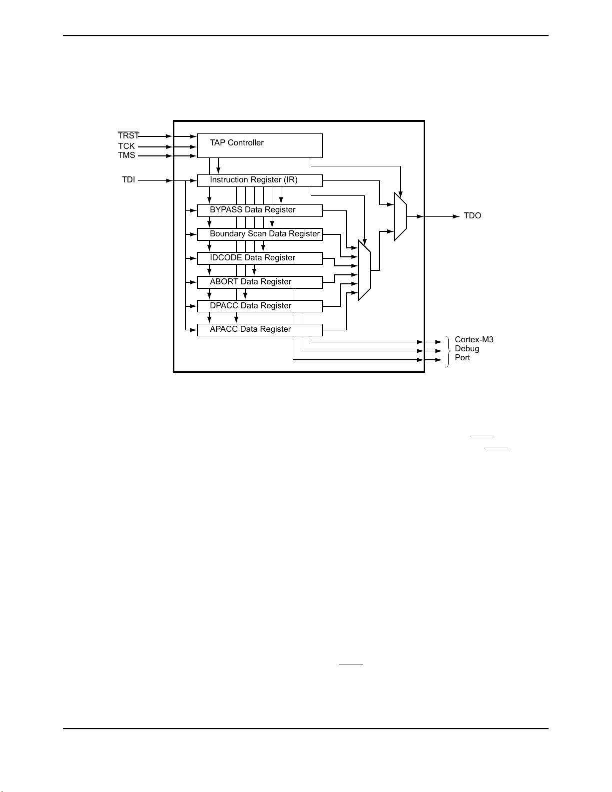
5.1 Block Diagram
Instruction Register (IR)
TAP Controller
BYPASS Data Register
Boundary Scan Data Register
IDCODE Data Register
ABORT Data Register
DPACC Data Register
APACC Data Register
TCK
TMS
TDI
TDO
Cortex-M3
Debug
Port
TRST
Figure 5-1. JTAG Module Block Diagram
Stellaris® LM3S1332 Microcontroller
5.2 Functional Description
A high-level conceptual drawing of the JTAG module is shown in Figure 5-1 on page 51. The JTAG
module is composed of the Test Access Port (TAP) controller and serial shift chains with parallel
update registers. The TAP controller is a simple state machine controlled by the TRST, TCK and
TMS inputs. The current state of the TAP controller depends on the current value of TRST and the
sequence of values captured on TMS at the rising edge of TCK. The TAP controller determines when
the serial shift chains capture new data, shift data from TDI towards TDO, and update the parallel
load registers. The current state of the TAP controller also determines whether the Instruction
Register (IR) chain or one of the Data Register (DR) chains is being accessed.
The serial shift chains with parallel load registers are comprised of a single Instruction Register (IR)
chain and multiple Data Register (DR) chains. The current instruction loaded in the parallel load
register determines which DR chain is captured, shifted, or updated during the sequencing of the
TAP controller.
Some instructions, like EXTEST and INTEST, operate on data currently in a DR chain and do not
capture, shift, or update any of the chains. Instructions that are not implemented decode to the
BYPASS instruction to ensure that the serial path between TDI and TDO is always connected (see
Table 5-2 on page 57 for a list of implemented instructions).
See “JTAG and Boundary Scan” on page 430 for JTAG timing diagrams.
5.2.1 JTAG Interface Pins
The JTAG interface consists of five standard pins: TRST,TCK, TMS, TDI, and TDO. These pins and
their associated reset state are given in Table 5-1 on page 52. Detailed information on each pin
follows.
51June 23, 2010
Texas Instruments-Production Data
Page 52

JTAG Interface
Table 5-1. JTAG Port Pins Reset State
5.2.1.1 Test Reset Input (TRST)
The TRST pin is an asynchronous active Low input signal for initializing and resetting the JTAG TAP
controller and associated JTAG circuitry. When TRST is asserted, the TAP controller resets to the
Test-Logic-Reset state and remains there while TRST is asserted. When the TAP controller enters
the Test-Logic-Reset state, the JTAG Instruction Register (IR) resets to the default instruction,
IDCODE.
By default, the internal pull-up resistor on the TRST pin is enabled after reset. Changes to the pull-up
resistor settings on GPIO Port B should ensure that the internal pull-up resistor remains enabled
on PB7/TRST; otherwise JTAG communication could be lost.
Drive ValueDrive StrengthInternal Pull-DownInternal Pull-UpData DirectionPin Name
N/AN/ADisabledEnabledInputTRST
N/AN/ADisabledEnabledInputTCK
N/AN/ADisabledEnabledInputTMS
N/AN/ADisabledEnabledInputTDI
High-Z2-mA driverDisabledEnabledOutputTDO
5.2.1.2 Test Clock Input (TCK)
The TCK pin is the clock for the JTAG module. This clock is provided so the test logic can operate
independently of any other system clocks. In addition, it ensures that multiple JTAG TAP controllers
that are daisy-chained together can synchronously communicate serial test data between
components. During normal operation, TCK is driven by a free-running clock with a nominal 50%
duty cycle. When necessary, TCK can be stopped at 0 or 1 for extended periods of time. While TCK
is stopped at 0 or 1, the state of the TAP controller does not change and data in the JTAG Instruction
and Data Registers is not lost.
By default, the internal pull-up resistor on the TCK pin is enabled after reset. This assures that no
clocking occurs if the pin is not driven from an external source. The internal pull-up and pull-down
resistors can be turned off to save internal power as long as the TCK pin is constantly being driven
by an external source.
5.2.1.3 Test Mode Select (TMS)
The TMS pin selects the next state of the JTAG TAP controller. TMS is sampled on the rising edge
of TCK. Depending on the current TAP state and the sampled value of TMS, the next state is entered.
Because the TMS pin is sampled on the rising edge of TCK, the IEEE Standard 1149.1 expects the
value on TMS to change on the falling edge of TCK.
Holding TMS high for five consecutive TCK cycles drives the TAP controller state machine to the
Test-Logic-Reset state. When the TAP controller enters the Test-Logic-Reset state, the JTAG
Instruction Register (IR) resets to the default instruction, IDCODE. Therefore, this sequence can
be used as a reset mechanism, similar to asserting TRST. The JTAG Test Access Port state machine
can be seen in its entirety in Figure 5-2 on page 54.
By default, the internal pull-up resistor on the TMS pin is enabled after reset. Changes to the pull-up
resistor settings on GPIO Port C should ensure that the internal pull-up resistor remains enabled
on PC1/TMS; otherwise JTAG communication could be lost.
June 23, 201052
Texas Instruments-Production Data
Page 53

5.2.1.4 Test Data Input (TDI)
The TDI pin provides a stream of serial information to the IR chain and the DR chains. TDI is
sampled on the rising edge of TCK and, depending on the current TAP state and the current
instruction, presents this data to the proper shift register chain. Because the TDI pin is sampled on
the rising edge of TCK, the IEEE Standard 1149.1 expects the value on TDI to change on the falling
edge of TCK.
By default, the internal pull-up resistor on the TDI pin is enabled after reset. Changes to the pull-up
resistor settings on GPIO Port C should ensure that the internal pull-up resistor remains enabled
on PC2/TDI; otherwise JTAG communication could be lost.
5.2.1.5 Test Data Output (TDO)
The TDO pin provides an output stream of serial information from the IR chain or the DR chains.
The value of TDO depends on the current TAP state, the current instruction, and the data in the
chain being accessed. In order to save power when the JTAG port is not being used, the TDO pin
is placed in an inactive drive state when not actively shifting out data. Because TDO can be connected
to the TDI of another controller in a daisy-chain configuration, the IEEE Standard 1149.1 expects
the value on TDO to change on the falling edge of TCK.
By default, the internal pull-up resistor on the TDO pin is enabled after reset. This assures that the
pin remains at a constant logic level when the JTAG port is not being used. The internal pull-up and
pull-down resistors can be turned off to save internal power if a High-Z output value is acceptable
during certain TAP controller states.
Stellaris® LM3S1332 Microcontroller
5.2.2 JTAG TAP Controller
The JTAG TAP controller state machine is shown in Figure 5-2 on page 54. The TAP controller
state machine is reset to the Test-Logic-Reset state on the assertion of a Power-On-Reset (POR)
or the assertion of TRST. Asserting the correct sequence on the TMS pin allows the JTAG module
to shift in new instructions, shift in data, or idle during extended testing sequences. For detailed
information on the function of the TAP controller and the operations that occur in each state, please
refer to IEEE Standard 1149.1.
Texas Instruments-Production Data
53June 23, 2010
Page 54
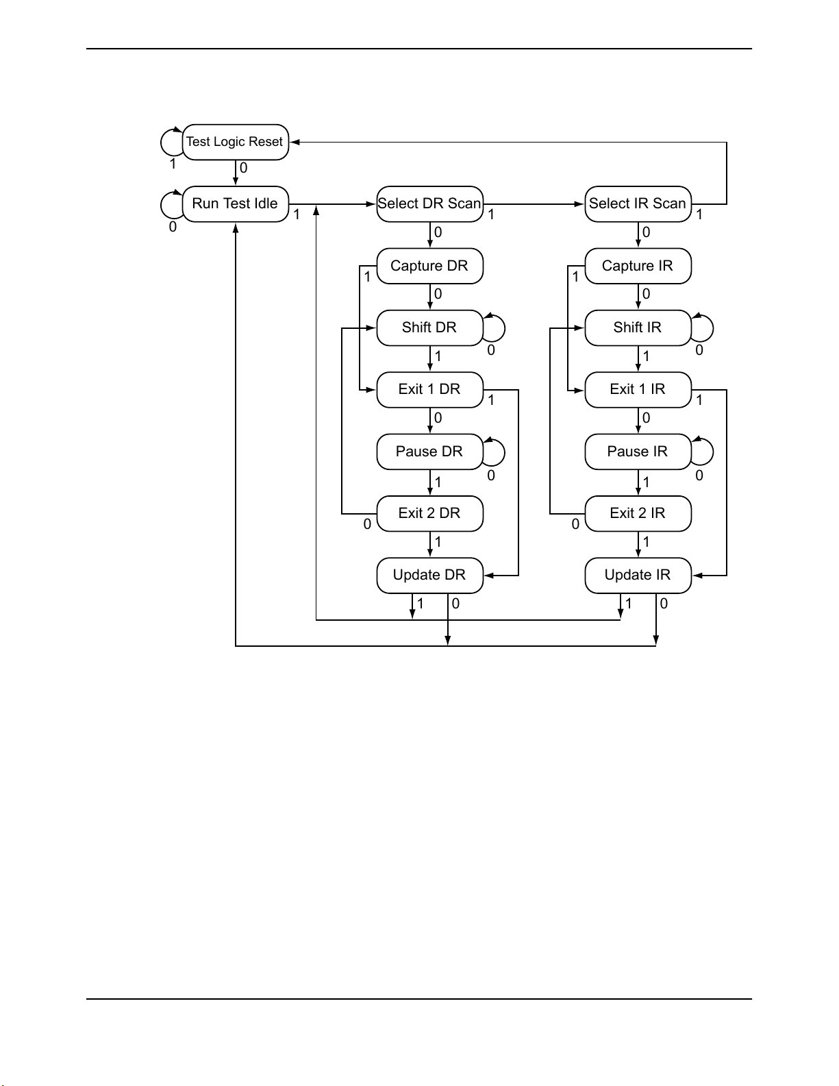
Test Logic Reset
Run Test Idle Select DR Scan Select IR Scan
Capture DR Capture IR
Shift DR Shift IR
Exit 1 DR Exit 1 IR
Exit 2 DR Exit 2 IR
Pause DR Pause IR
Update DR Update IR
1 11
1 1
1
1 1
1 1
1 1
1 1
1 10 0
00
00
0 0
0 0
0 0
00
0
0
JTAG Interface
Figure 5-2. Test Access Port State Machine
5.2.3 Shift Registers
The Shift Registers consist of a serial shift register chain and a parallel load register. The serial shift
register chain samples specific information during the TAP controller’s CAPTURE states and allows
this information to be shifted out of TDO during the TAP controller’s SHIFT states. While the sampled
data is being shifted out of the chain on TDO, new data is being shifted into the serial shift register
on TDI. This new data is stored in the parallel load register during the TAP controller’s UPDATE
states. Each of the shift registers is discussed in detail in “Register Descriptions” on page 57.
5.2.4 Operational Considerations
There are certain operational considerations when using the JTAG module. Because the JTAG pins
can be programmed to be GPIOs, board configuration and reset conditions on these pins must be
considered. In addition, because the JTAG module has integrated ARM Serial Wire Debug, the
method for switching between these two operational modes is described below.
Texas Instruments-Production Data
June 23, 201054
Page 55

5.2.4.1 GPIO Functionality
When the controller is reset with either a POR or RST, the JTAG/SWD port pins default to their
JTAG/SWD configurations. The default configuration includes enabling digital functionality (setting
GPIODEN to 1), enabling the pull-up resistors (setting GPIOPUR to 1), and enabling the alternate
hardware function (setting GPIOAFSEL to 1) for the PB7 and PC[3:0] JTAG/SWD pins.
It is possible for software to configure these pins as GPIOs after reset by writing 0s to PB7 and
PC[3:0] in the GPIOAFSEL register. If the user does not require the JTAG/SWD port for debugging
or board-level testing, this provides five more GPIOs for use in the design.
Caution – It is possible to create a software sequence that prevents the debugger from connecting to
the Stellaris®microcontroller. If the program code loaded into ash immediately changes the JTAG
pins to their GPIO functionality, the debugger may not have enough time to connect and halt the
controller before the JTAG pin functionality switches. This may lock the debugger out of the part. This
can be avoided with a software routine that restores JTAG functionality based on an external or software
trigger.
The GPIO commit control registers provide a layer of protection against accidental programming of
critical hardware peripherals. Protection is currently provided for the five JTAG/SWD pins (PB7 and
PC[3:0]). Writes to protected bits of the GPIO Alternate Function Select (GPIOAFSEL) register
(see page 186) are not committed to storage unless the GPIO Lock (GPIOLOCK) register (see
page 196) has been unlocked and the appropriate bits of the GPIO Commit (GPIOCR) register (see
page 197) have been set to 1.
Stellaris® LM3S1332 Microcontroller
Recovering a "Locked" Device
Note: The mass erase of the flash memory caused by the below sequence erases the entire flash
memory, regardless of the settings in the Flash Memory Protection Program Enable n
(FMPPEn) registers. Performing the sequence below does not affect the nonvolatile registers
discussed in “Nonvolatile Register Programming” on page 147.
If software configures any of the JTAG/SWD pins as GPIO and loses the ability to communicate
with the debugger, there is a debug sequence that can be used to recover the device. Performing
a total of ten JTAG-to-SWD and SWD-to-JTAG switch sequences while holding the device in reset
mass erases the flash memory. The sequence to recover the device is:
1. Assert and hold the RST signal.
2. Perform the JTAG-to-SWD switch sequence.
3. Perform the SWD-to-JTAG switch sequence.
4. Perform the JTAG-to-SWD switch sequence.
5. Perform the SWD-to-JTAG switch sequence.
6. Perform the JTAG-to-SWD switch sequence.
7. Perform the SWD-to-JTAG switch sequence.
8. Perform the JTAG-to-SWD switch sequence.
9. Perform the SWD-to-JTAG switch sequence.
10. Perform the JTAG-to-SWD switch sequence.
Texas Instruments-Production Data
55June 23, 2010
Page 56

JTAG Interface
11. Perform the SWD-to-JTAG switch sequence.
12. Release the RST signal.
13. Wait 400 ms.
14. Power-cycle the device.
The JTAG-to-SWD and SWD-to-JTAG switch sequences are described in “ARM Serial Wire Debug
(SWD)” on page 56. When performing switch sequences for the purpose of recovering the debug
capabilities of the device, only steps 1 and 2 of the switch sequence in the section called
“JTAG-to-SWD Switching” on page 56 must be performed.
5.2.4.2 Communication with JTAG/SWD
Because the debug clock and the system clock can be running at different frequencies, care must
be taken to maintain reliable communication with the JTAG/SWD interface. In the Capture-DR state,
the result of the previous transaction, if any, is returned, together with a 3-bit ACK response. Software
should check the ACK response to see if the previous operation has completed before initiating a
new transaction. Alternatively, if the system clock is at least 8 times faster than the debug clock
(TCK or SWCLK), the previous operation has enough time to complete and the ACK bits do not have
to be checked.
5.2.4.3 ARM Serial Wire Debug (SWD)
In order to seamlessly integrate the ARM Serial Wire Debug (SWD) functionality, a serial-wire
debugger must be able to connect to the Cortex-M3 core without having to perform, or have any
knowledge of, JTAG cycles. This is accomplished with a SWD preamble that is issued before the
SWD session begins.
The switching preamble used to enable the SWD interface of the SWJ-DP module starts with the
TAP controller in the Test-Logic-Reset state. From here, the preamble sequences the TAP controller
through the following states: Run Test Idle, Select DR, Select IR, Test Logic Reset, Test Logic
Reset, Run Test Idle, Run Test Idle, Select DR, Select IR, Test Logic Reset, Test Logic Reset, Run
Test Idle, Run Test Idle, Select DR, Select IR, and Test Logic Reset states.
Stepping through this sequences of the TAP state machine enables the SWD interface and disables
the JTAG interface. For more information on this operation and the SWD interface, see the ARM®
Cortex™-M3 Technical Reference Manual and the ARM® CoreSight Technical Reference Manual.
Because this sequence is a valid series of JTAG operations that could be issued, the ARM JTAG
TAP controller is not fully compliant to the IEEE Standard 1149.1. This is the only instance where
the ARM JTAG TAP controller does not meet full compliance with the specification. Due to the low
probability of this sequence occurring during normal operation of the TAP controller, it should not
affect normal performance of the JTAG interface.
JTAG-to-SWD Switching
To switch the operating mode of the Debug Access Port (DAP) from JTAG to SWD mode, the
external debug hardware must send the switching preamble to the device. The 16-bit switch sequence
for switching to SWD mode is defined as b1110011110011110, transmitted LSB first. This can also
be represented as 16'hE79E when transmitted LSB first. The complete switch sequence should
consist of the following transactions on the TCK/SWCLK and TMS/SWDIO signals:
1. Send at least 50 TCK/SWCLK cycles with TMS/SWDIO set to 1. This ensures that both JTAG and
SWD are in their reset/idle states.
June 23, 201056
Texas Instruments-Production Data
Page 57

Stellaris® LM3S1332 Microcontroller
2. Send the 16-bit JTAG-to-SWD switch sequence, 16'hE79E.
3. Send at least 50 TCK/SWCLK cycles with TMS/SWDIO set to 1. This ensures that if SWJ-DP was
already in SWD mode, before sending the switch sequence, the SWD goes into the line reset
state.
SWD-to-JTAG Switching
To switch the operating mode of the Debug Access Port (DAP) from SWD to JTAG mode, the
external debug hardware must send a switch sequence to the device. The 16-bit switch sequence
for switching to JTAG mode is defined as b1110011100111100, transmitted LSB first. This can also
be represented as 16'hE73C when transmitted LSB first. The complete switch sequence should
consist of the following transactions on the TCK/SWCLK and TMS/SWDIO signals:
1. Send at least 50 TCK/SWCLK cycles with TMS/SWDIO set to 1. This ensures that both JTAG and
SWD are in their reset/idle states.
2. Send the 16-bit SWD-to-JTAG switch sequence, 16'hE73C.
3. Send at least 5 TCK/SWCLK cycles with TMS/SWDIO set to 1. This ensures that if SWJ-DP was
already in JTAG mode, before sending the switch sequence, the JTAG goes into the Test Logic
Reset state.
5.3 Initialization and Configuration
After a Power-On-Reset or an external reset (RST), the JTAG pins are automatically configured for
JTAG communication. No user-defined initialization or configuration is needed. However, if the user
application changes these pins to their GPIO function, they must be configured back to their JTAG
functionality before JTAG communication can be restored. This is done by enabling the five JTAG
pins (PB7 and PC[3:0]) for their alternate function using the GPIOAFSEL register. In addition to
enabling the alternate functions, any other changes to the GPIO pad configurations on the five JTAG
pins (PB7 andPC[3:0]) should be reverted to their default settings.
5.4 Register Descriptions
There are no APB-accessible registers in the JTAG TAP Controller or Shift Register chains. The
registers within the JTAG controller are all accessed serially through the TAP Controller. The registers
can be broken down into two main categories: Instruction Registers and Data Registers.
5.4.1 Instruction Register (IR)
The JTAG TAP Instruction Register (IR) is a four-bit serial scan chain connected between the JTAG
TDI and TDO pins with a parallel load register. When the TAP Controller is placed in the correct
states, bits can be shifted into the Instruction Register. Once these bits have been shifted into the
chain and updated, they are interpreted as the current instruction. The decode of the Instruction
Register bits is shown in Table 5-2 on page 57. A detailed explanation of each instruction, along
with its associated Data Register, follows.
Table 5-2. JTAG Instruction Register Commands
DescriptionInstructionIR[3:0]
EXTEST0000
INTEST0001
Texas Instruments-Production Data
Drives the values preloaded into the Boundary Scan Chain by the
SAMPLE/PRELOAD instruction onto the pads.
Drives the values preloaded into the Boundary Scan Chain by the
SAMPLE/PRELOAD instruction into the controller.
57June 23, 2010
Page 58

JTAG Interface
Table 5-2. JTAG Instruction Register Commands (continued)
SAMPLE / PRELOAD0010
5.4.1.1 EXTEST Instruction
The EXTEST instruction is not associated with its own Data Register chain. The EXTEST instruction
uses the data that has been preloaded into the Boundary Scan Data Register using the
SAMPLE/PRELOAD instruction. When the EXTEST instruction is present in the Instruction Register,
the preloaded data in the Boundary Scan Data Register associated with the outputs and output
enables are used to drive the GPIO pads rather than the signals coming from the core. This allows
tests to be developed that drive known values out of the controller, which can be used to verify
connectivity. While the EXTEST instruction is present in the Instruction Register, the Boundary Scan
Data Register can be accessed to sample and shift out the current data and load new data into the
Boundary Scan Data Register.
DescriptionInstructionIR[3:0]
Captures the current I/O values and shifts the sampled values out of the
Boundary Scan Chain while new preload data is shifted in.
Shifts data into the ARM Debug Port Abort Register.ABORT1000
Shifts data into and out of the ARM DP Access Register.DPACC1010
Shifts data into and out of the ARM AC Access Register.APACC1011
IDCODE1110
ReservedAll Others
Loads manufacturing information defined by the IEEE Standard 1149.1
into the IDCODE chain and shifts it out.
Connects TDI to TDO through a single Shift Register chain.BYPASS1111
Defaults to the BYPASS instruction to ensure that TDI is always connected
to TDO.
5.4.1.2 INTEST Instruction
The INTEST instruction is not associated with its own Data Register chain. The INTEST instruction
uses the data that has been preloaded into the Boundary Scan Data Register using the
SAMPLE/PRELOAD instruction. When the INTEST instruction is present in the Instruction Register,
the preloaded data in the Boundary Scan Data Register associated with the inputs are used to drive
the signals going into the core rather than the signals coming from the GPIO pads. This allows tests
to be developed that drive known values into the controller, which can be used for testing. It is
important to note that although the RST input pin is on the Boundary Scan Data Register chain, it
is only observable. While the INTEXT instruction is present in the Instruction Register, the Boundary
Scan Data Register can be accessed to sample and shift out the current data and load new data
into the Boundary Scan Data Register.
5.4.1.3 SAMPLE/PRELOAD Instruction
The SAMPLE/PRELOAD instruction connects the Boundary Scan Data Register chain between
TDI and TDO. This instruction samples the current state of the pad pins for observation and preloads
new test data. Each GPIO pad has an associated input, output, and output enable signal. When the
TAP controller enters the Capture DR state during this instruction, the input, output, and output-enable
signals to each of the GPIO pads are captured. These samples are serially shifted out of TDO while
the TAP controller is in the Shift DR state and can be used for observation or comparison in various
tests.
While these samples of the inputs, outputs, and output enables are being shifted out of the Boundary
Scan Data Register, new data is being shifted into the Boundary Scan Data Register from TDI.
Once the new data has been shifted into the Boundary Scan Data Register, the data is saved in the
parallel load registers when the TAP controller enters the Update DR state. This update of the
parallel load register preloads data into the Boundary Scan Data Register that is associated with
Texas Instruments-Production Data
June 23, 201058
Page 59

each input, output, and output enable. This preloaded data can be used with the EXTEST and
INTEST instructions to drive data into or out of the controller. Please see “Boundary Scan Data
Register” on page 60 for more information.
5.4.1.4 ABORT Instruction
The ABORT instruction connects the associated ABORT Data Register chain between TDI and
TDO. This instruction provides read and write access to the ABORT Register of the ARM Debug
Access Port (DAP). Shifting the proper data into this Data Register clears various error bits or initiates
a DAP abort of a previous request. Please see the “ABORT Data Register” on page 61 for more
information.
5.4.1.5 DPACC Instruction
The DPACC instruction connects the associated DPACC Data Register chain between TDI and
TDO. This instruction provides read and write access to the DPACC Register of the ARM Debug
Access Port (DAP). Shifting the proper data into this register and reading the data output from this
register allows read and write access to the ARM debug and status registers. Please see “DPACC
Data Register” on page 61 for more information.
5.4.1.6 APACC Instruction
Stellaris® LM3S1332 Microcontroller
The APACC instruction connects the associated APACC Data Register chain between TDI and
TDO. This instruction provides read and write access to the APACC Register of the ARM Debug
Access Port (DAP). Shifting the proper data into this register and reading the data output from this
register allows read and write access to internal components and buses through the Debug Port.
Please see “APACC Data Register” on page 61 for more information.
5.4.1.7 IDCODE Instruction
The IDCODE instruction connects the associated IDCODE Data Register chain between TDI and
TDO. This instruction provides information on the manufacturer, part number, and version of the
ARM core. This information can be used by testing equipment and debuggers to automatically
configure their input and output data streams. IDCODE is the default instruction that is loaded into
the JTAG Instruction Register when a Power-On-Reset (POR) is asserted, TRST is asserted, or the
Test-Logic-Reset state is entered. Please see “IDCODE Data Register” on page 60 for more
information.
5.4.1.8 BYPASS Instruction
The BYPASS instruction connects the associated BYPASS Data Register chain between TDI and
TDO. This instruction is used to create a minimum length serial path between the TDI and TDO ports.
The BYPASS Data Register is a single-bit shift register. This instruction improves test efficiency by
allowing components that are not needed for a specific test to be bypassed in the JTAG scan chain
by loading them with the BYPASS instruction. Please see “BYPASS Data Register” on page 60 for
more information.
5.4.2 Data Registers
The JTAG module contains six Data Registers. These include: IDCODE, BYPASS, Boundary Scan,
APACC, DPACC, and ABORT serial Data Register chains. Each of these Data Registers is discussed
in the following sections.
59June 23, 2010
Texas Instruments-Production Data
Page 60

Version Part Number Manufacturer ID 1
31 28 27 12 11 1 0
TDOTDI
0
TDOTDI
0
JTAG Interface
5.4.2.1 IDCODE Data Register
The format for the 32-bit IDCODE Data Register defined by the IEEE Standard 1149.1 is shown in
Figure 5-3 on page 60. The standard requires that every JTAG-compliant device implement either
the IDCODE instruction or the BYPASS instruction as the default instruction. The LSB of the IDCODE
Data Register is defined to be a 1 to distinguish it from the BYPASS instruction, which has an LSB
of 0. This allows auto configuration test tools to determine which instruction is the default instruction.
The major uses of the JTAG port are for manufacturer testing of component assembly, and program
development and debug. To facilitate the use of auto-configuration debug tools, the IDCODE
instruction outputs a value of 0x3BA0.0477. This allows the debuggers to automatically configure
themselves to work correctly with the Cortex-M3 during debug.
Figure 5-3. IDCODE Register Format
5.4.2.2 BYPASS Data Register
The format for the 1-bit BYPASS Data Register defined by the IEEE Standard 1149.1 is shown in
Figure 5-4 on page 60. The standard requires that every JTAG-compliant device implement either
the BYPASS instruction or the IDCODE instruction as the default instruction. The LSB of the BYPASS
Data Register is defined to be a 0 to distinguish it from the IDCODE instruction, which has an LSB
of 1. This allows auto configuration test tools to determine which instruction is the default instruction.
Figure 5-4. BYPASS Register Format
5.4.2.3 Boundary Scan Data Register
The format of the Boundary Scan Data Register is shown in Figure 5-5 on page 61. Each GPIO
pin, starting with a GPIO pin next to the JTAG port pins, is included in the Boundary Scan Data
Register. Each GPIO pin has three associated digital signals that are included in the chain. These
signals are input, output, and output enable, and are arranged in that order as can be seen in the
figure.
When the Boundary Scan Data Register is accessed with the SAMPLE/PRELOAD instruction, the
input, output, and output enable from each digital pad are sampled and then shifted out of the chain
to be verified. The sampling of these values occurs on the rising edge of TCK in the Capture DR
state of the TAP controller. While the sampled data is being shifted out of the Boundary Scan chain
in the Shift DR state of the TAP controller, new data can be preloaded into the chain for use with
the EXTEST and INTEST instructions. These instructions either force data out of the controller, with
the EXTEST instruction, or into the controller, with the INTEST instruction.
Texas Instruments-Production Data
June 23, 201060
Page 61

Figure 5-5. Boundary Scan Register Format
O
TDOTDI
O
I
N E
U
T
O
O
I
N E
U
T
O
O
I
N E
U
T
O
O
I
N E
U
T
I
N
...
...
RSTGPIO PB6 GPIO m GPIO m+1 G PIO n
5.4.2.4 APACC Data Register
The format for the 35-bit APACC Data Register defined by ARM is described in the ARM®
Cortex™-M3 Technical Reference Manual.
5.4.2.5 DPACC Data Register
The format for the 35-bit DPACC Data Register defined by ARM is described in the ARM®
Cortex™-M3 Technical Reference Manual.
5.4.2.6 ABORT Data Register
The format for the 35-bit ABORT Data Register defined by ARM is described in the ARM®
Cortex™-M3 Technical Reference Manual.
Stellaris® LM3S1332 Microcontroller
61June 23, 2010
Texas Instruments-Production Data
Page 62

System Control
6 System Control
System control determines the overall operation of the device. It provides information about the
device, controls the clocking to the core and individual peripherals, and handles reset detection and
reporting.
6.1 Functional Description
The System Control module provides the following capabilities:
■ Device identification (see “Device Identification” on page 62)
■ Local control, such as reset (see “Reset Control” on page 62), power (see “Power
Control” on page 65) and clock control (see “Clock Control” on page 66)
■ System control (Run, Sleep, and Deep-Sleep modes); see “System Control” on page 71
6.1.1 Device Identification
Several read-only registers provide software with information on the microcontroller, such as version,
part number, SRAM size, flash size, and other features. See the DID0, DID1, and DC0-DC4 registers.
6.1.2 Reset Control
This section discusses aspects of hardware functions during reset as well as system software
requirements following the reset sequence.
6.1.2.1 CMOD0 and CMOD1 Test-Mode Control Pins
Two pins, CMOD0 and CMOD1, are defined for internal use for testing the microcontroller during
manufacture. They have no end-user function and should not be used. The CMOD pins should be
connected to ground.
6.1.2.2 Reset Sources
The controller has five sources of reset:
1. External reset input pin (RST) assertion; see “External RST Pin” on page 63.
2. Power-on reset (POR); see “Power-On Reset (POR)” on page 62.
3. Internal brown-out (BOR) detector; see “Brown-Out Reset (BOR)” on page 64.
4. Software-initiated reset (with the software reset registers); see “Software Reset” on page 65.
5. A watchdog timer reset condition violation; see “Watchdog Timer Reset” on page 65.
After a reset, the Reset Cause (RESC) register is set with the reset cause. The bits in this register
are sticky and maintain their state across multiple reset sequences, except when an internal POR
is the cause, and then all the other bits in the RESC register are cleared except for the POR indicator.
6.1.2.3 Power-On Reset (POR)
Note: The power-on reset also resets the JTAG controller. An external reset does not.
June 23, 201062
Texas Instruments-Production Data
Page 63

The internal Power-On Reset (POR) circuit monitors the power supply voltage (VDD) and generates
PU
RST
Stellaris®
R
VDD
a reset signal to all of the internal logic including JTAG when the power supply ramp reaches a
threshold value (VTH). The microcontroller must be operating within the specified operating parameters
when the on-chip power-on reset pulse is complete. The 3.3-V power supply to the microcontroller
must reach 3.0 V within 10 msec of VDDcrossing 2.0 V to guarantee proper operation. For applications
that require the use of an external reset signal to hold the microcontroller in reset longer than the
internal POR, the RST input may be used as discussed in “External RST Pin” on page 63.
The Power-On Reset sequence is as follows:
1. The microcontroller waits for internal POR to go inactive.
2. The internal reset is released and the core loads from memory the initial stack pointer, the initial
program counter, and the first instruction designated by the program counter, and then begins
execution.
The internal POR is only active on the initial power-up of the microcontroller. The Power-On Reset
timing is shown in Figure 19-6 on page 433.
6.1.2.4 External RST Pin
Note: It is recommended that the trace for the RST signal must be kept as short as possible. Be
sure to place any components connected to the RST signal as close to the microcontroller
as possible.
Stellaris® LM3S1332 Microcontroller
If the application only uses the internal POR circuit, the RST input must be connected to the power
supply (VDD) through an optional pull-up resistor (0 to 100K Ω) as shown in Figure 6-1 on page 63.
Figure 6-1. Basic RST Configuration
RPU= 0 to 100 kΩ
The external reset pin (RST) resets the microcontroller including the core and all the on-chip
peripherals except the JTAG TAP controller (see “JTAG Interface” on page 50). The external reset
sequence is as follows:
1. The external reset pin (RST) is asserted for the duration specified by T
and then de-asserted
MIN
(see “Reset” on page 432).
2. The internal reset is released and the core loads from memory the initial stack pointer, the initial
program counter, and the first instruction designated by the program counter, and then begins
execution.
To improve noise immunity and/or to delay reset at power up, the RST input may be connected to
an RC network as shown in Figure 6-2 on page 64.
Texas Instruments-Production Data
63June 23, 2010
Page 64

PU
C
1
RST
Stellaris®
R
VDD
PU
C
1
R
S
RST
Stellaris®
R
VDD
System Control
Figure 6-2. External Circuitry to Extend Power-On Reset
RPU= 1 kΩ to 100 kΩ
C1= 1 nF to 10 µF
If the application requires the use of an external reset switch, Figure 6-3 on page 64 shows the
proper circuitry to use.
Figure 6-3. Reset Circuit Controlled by Switch
Typical RPU= 10 kΩ
Typical RS= 470 Ω
C1= 10 nF
The RPUand C1components define the power-on delay.
The external reset timing is shown in Figure 19-5 on page 433.
6.1.2.5 Brown-Out Reset (BOR)
A drop in the input voltage resulting in the assertion of the internal brown-out detector can be used
to reset the controller. This is initially disabled and may be enabled by software.
The system provides a brown-out detection circuit that triggers if the power supply (VDD) drops
below a brown-out threshold voltage (V
generate a controller interrupt or a system reset.
Brown-out resets are controlled with the Power-On and Brown-Out Reset Control (PBORCTL)
register. The BORIOR bit in the PBORCTL register must be set for a brown-out condition to trigger
a reset.
The brown-out reset is equivalent to an assertion of the external RST input and the reset is held
active until the proper VDDlevel is restored. The RESC register can be examined in the reset interrupt
). If a brown-out condition is detected, the system may
BTH
Texas Instruments-Production Data
June 23, 201064
Page 65

handler to determine if a Brown-Out condition was the cause of the reset, thus allowing software to
determine what actions are required to recover.
The internal Brown-Out Reset timing is shown in Figure 19-7 on page 433.
6.1.2.6 Software Reset
Software can reset a specific peripheral or generate a reset to the entire system .
Peripherals can be individually reset by software via three registers that control reset signals to each
peripheral (see the SRCRn registers). If the bit position corresponding to a peripheral is set and
subsequently cleared, the peripheral is reset. The encoding of the reset registers is consistent with
the encoding of the clock gating control for peripherals and on-chip functions (see “System
Control” on page 71). Note that all reset signals for all clocks of the specified unit are asserted as
a result of a software-initiated reset.
The entire system can be reset by software by setting the SYSRESETREQ bit in the Cortex-M3
Application Interrupt and Reset Control register resets the entire system including the core. The
software-initiated system reset sequence is as follows:
1. A software system reset is initiated by writing the SYSRESETREQ bit in the ARM Cortex-M3
Application Interrupt and Reset Control register.
Stellaris® LM3S1332 Microcontroller
2. An internal reset is asserted.
3. The internal reset is deasserted and the controller loads from memory the initial stack pointer,
the initial program counter, and the first instruction designated by the program counter, and
then begins execution.
The software-initiated system reset timing is shown in Figure 19-8 on page 433.
6.1.2.7 Watchdog Timer Reset
The watchdog timer module's function is to prevent system hangs. The watchdog timer can be
configured to generate an interrupt to the controller on its first time-out, and to generate a reset
signal on its second time-out.
After the first time-out event, the 32-bit counter is reloaded with the value of the Watchdog Timer
Load (WDTLOAD) register, and the timer resumes counting down from that value. If the timer counts
down to its zero state again before the first time-out interrupt is cleared, and the reset signal has
been enabled, the watchdog timer asserts its reset signal to the system. The watchdog timer reset
sequence is as follows:
1. The watchdog timer times out for the second time without being serviced.
2. An internal reset is asserted.
3. The internal reset is released and the controller loads from memory the initial stack pointer, the
initial program counter, the first instruction designated by the program counter, and begins
execution.
The watchdog reset timing is shown in Figure 19-9 on page 434.
6.1.3 Power Control
The Stellaris®microcontroller provides an integrated LDO regulator that may be used to provide
power to the majority of the controller's internal logic. For power reduction, the LDO regulator provides
65June 23, 2010
Texas Instruments-Production Data
Page 66

I/O Buffers
Analog circuits
(ADC, analog
comparators)
Low-noise
LDO
Internal
Logic and PLL
GND
GND
GND
GND
GNDA
GND
GND
GND
GND
VDD
VDD
VDD
VDD
VDDA
VDDA
VDD25
VDD25
VDD25
VDD25
LDO
+3.3V
GNDA
System Control
software a mechanism to adjust the regulated value, in small increments (VSTEP), over the range
of 2.25 V to 2.75 V (inclusive)—or 2.5 V ± 10%. The adjustment is made by changing the value of
the VADJ field in the LDO Power Control (LDOPCTL) register.
Figure 6-4 on page 66 shows the power architecture.
Note: On the printed circuit board, use the LDO output as the source of VDD25 input. In addition,
Figure 6-4. Power Architecture
the LDO requires decoupling capacitors. See “On-Chip Low Drop-Out (LDO) Regulator
Characteristics” on page 426.
6.1.4 Clock Control
6.1.4.1 Fundamental Clock Sources
System control determines the control of clocks in this part.
There are multiple clock sources for use in the device:
Texas Instruments-Production Data
June 23, 201066
Page 67
Stellaris® LM3S1332 Microcontroller
■ Internal Oscillator (IOSC). The internal oscillator is an on-chip clock source. It does not require
the use of any external components. The frequency of the internal oscillator is 12 MHz ± 30%.
Applications that do not depend on accurate clock sources may use this clock source to reduce
system cost. The internal oscillator is the clock source the device uses during and following POR.
If the main oscillator is required, software must enable the main oscillator following reset and
allow the main oscillator to stabilize before changing the clock reference.
■ Main Oscillator (MOSC). The main oscillator provides a frequency-accurate clock source by
one of two means: an external single-ended clock source is connected to the OSC0 input pin, or
an external crystal is connected across the OSC0 input and OSC1 output pins. If the PLL is being
used, the crystal value must be one of the supported frequencies between 3.579545 MHz through
8.192 MHz (inclusive). If the PLL is not being used, the crystal may be any one of the supported
frequencies between 1 MHz and 8.192 MHz. The single-ended clock source range is from DC
through the specified speed of the device. The supported crystals are listed in the XTAL bit field
in the RCC register (see page 83).
■ Internal 30-kHz Oscillator. The internal 30-kHz oscillator is similar to the internal oscillator,
except that it provides an operational frequency of 30 kHz ± 50%. It is intended for use during
Deep-Sleep power-saving modes. This power-savings mode benefits from reduced internal
switching and also allows the main oscillator to be powered down.
■ External Real-Time Oscillator. The external real-time oscillator provides a low-frequency,
accurate clock reference. It is intended to provide the system with a real-time clock source. The
real-time oscillator is part of the Hibernation Module (see “Hibernation Module” on page 124) and
may also provide an accurate source of Deep-Sleep or Hibernate mode power savings.
The internal system clock (SysClk), is derived from any of the above sources plus two others: the
output of the main internal PLL, and the internal oscillator divided by four (3 MHz ± 30%). The
frequency of the PLL clock reference must be in the range of 3.579545 MHz to 8.192 MHz (inclusive).
Table 6-1 on page 67 shows how the various clock sources can be used in a system.
Table 6-1. Clock Source Options
MHz)
6.1.4.2 Clock Configuration
The Run-Mode Clock Configuration (RCC) and Run-Mode Clock Configuration 2 (RCC2)
registers provide control for the system clock. The RCC2 register is provided to extend fields that
offer additional encodings over the RCC register. When used, the RCC2 register field values are
used by the logic over the corresponding field in the RCC register. In particular, RCC2 provides for
a larger assortment of clock configuration options. These registers control the following clock
functionality:
Used as SysClk?Drive PLL?Clock Source
BYPASS = 1, OSCSRC = 0x1YesBYPASS = 1NoInternal Oscillator (12 MHz)
BYPASS = 1, OSCSRC = 0x2YesBYPASS = 1NoInternal Oscillator divide by 4 (3
YesMain Oscillator
0x0
BYPASS = 1, OSCSRC = 0x0YesBYPASS = 0, OSCSRC =
BYPASS = 1, OSCSRC = 0x3YesBYPASS = 1NoInternal 30-kHz Oscillator
BYPASS = 1, OSCSRC2 = 0x7YesBYPASS = 1NoExternal Real-Time Oscillator
■ Source of clocks in sleep and deep-sleep modes
■ System clock derived from PLL or other clock source
Texas Instruments-Production Data
67June 23, 2010
Page 68
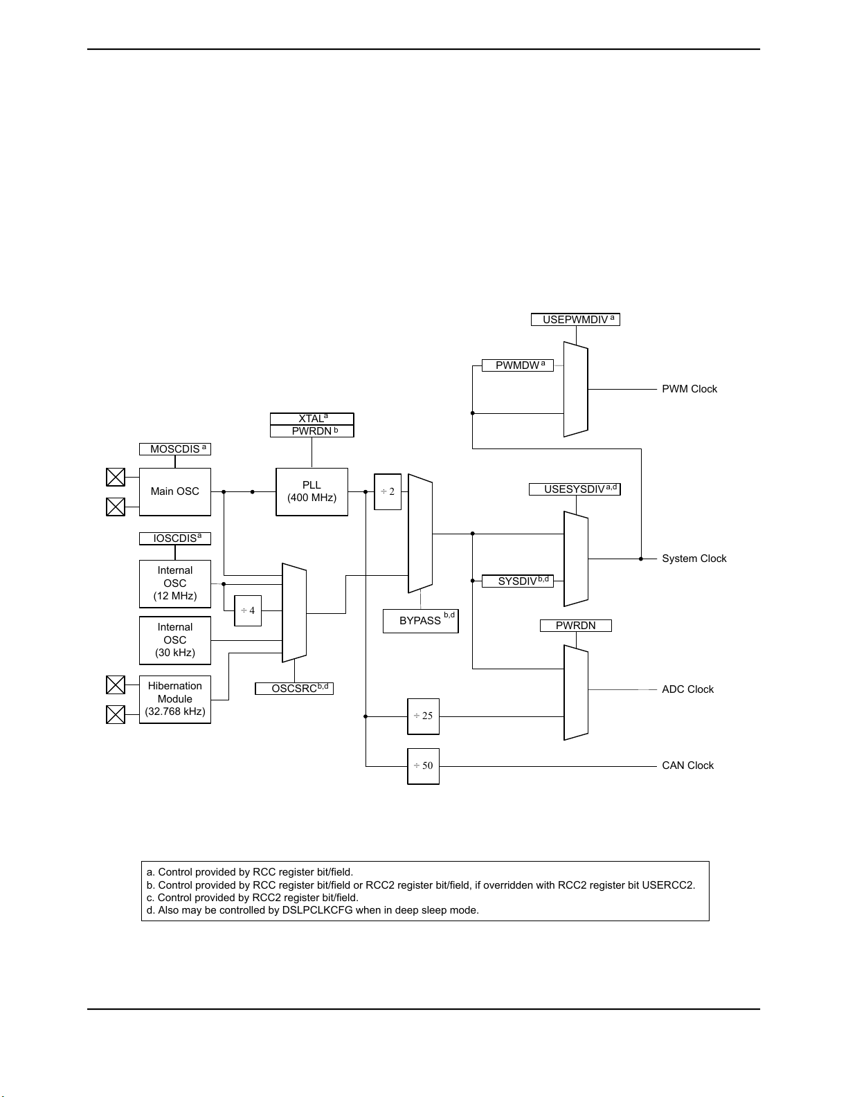
PLL
(400 MHz)
Main OSC
Internal
OSC
(12 MHz)
Internal
OSC
(30 kHz)
÷ 4
Hibernation
Module
(32.768 kHz)
÷ 25
PWRDN
ADC Clock
System Clock
XTAL
a
PWRDN
b
MOSCDIS
a
IOSCDIS
a
OSCSRC
b,d
BYPASS
b,d
SYSDIV
b,d
USESYSDIV
a,d
PWMDW
a
USEPWMDIV
a
PWM Clock
a. Control provided by RCC register bit/field.
b. Control provided by RCC register bit/field or RCC2 register bit/field, if overridden with RCC2 register bit USERCC2.
c. Control provided by RCC2 register bit/field.
d. Also may be controlled by DSLPCLKCFG when in deep sleep mode.
÷ 2
÷ 50 CAN Clock
System Control
■ Enabling/disabling of oscillators and PLL
■ Clock divisors
■ Crystal input selection
Figure 6-5 on page 68 shows the logic for the main clock tree. The peripheral blocks are driven by
the system clock signal and can be individually enabled/disabled. The ADC clock signal is
automatically divided down to 16 MHz for proper ADC operation.
Note: When the ADC module is in operation, the system clock must be at least 16 MHz.
Figure 6-5. Main Clock Tree
Note: The figure above shows all features available on all Stellaris® Fury-class devices.
Texas Instruments-Production Data
June 23, 201068
Page 69
Stellaris® LM3S1332 Microcontroller
In the RCC register, the SYSDIV field specifies which divisor is used to generate the system clock
from either the PLL output or the oscillator source (depending on how the BYPASS bit in this register
is configured). When using the PLL, the VCO frequency of 400 MHz is predivided by 2 before the
divisor is applied. Table 6-2 shows how the SYSDIV encoding affects the system clock frequency,
depending on whether the PLL is used (BYPASS=0) or another clock source is used (BYPASS=1).
The divisor is equivalent to the SYSDIV encoding plus 1. For a list of possible clock sources, see
Table 6-1 on page 67.
Table 6-2. Possible System Clock Frequencies Using the SYSDIV Field
DivisorSYSDIV
(BYPASS=0)
a. This parameter is used in functions such as SysCtlClockSet() in the Stellaris Peripheral Driver Library.
b. SYSCTL_SYSDIV_1 does not set the USESYSDIV bit. As a result, using this parameter without enabling the PLL results
in the system clock having the same frequency as the clock source.
Frequency (BYPASS=1)Frequency
Clock source frequency/2reserved/10x0
StellarisWare Parameter
SYSCTL_SYSDIV_1
SYSCTL_SYSDIV_2Clock source frequency/2reserved/20x1
SYSCTL_SYSDIV_3Clock source frequency/3reserved/30x2
SYSCTL_SYSDIV_4Clock source frequency/450 MHz/40x3
SYSCTL_SYSDIV_5Clock source frequency/540 MHz/50x4
SYSCTL_SYSDIV_6Clock source frequency/633.33 MHz/60x5
SYSCTL_SYSDIV_7Clock source frequency/728.57 MHz/70x6
SYSCTL_SYSDIV_8Clock source frequency/825 MHz/80x7
SYSCTL_SYSDIV_9Clock source frequency/922.22 MHz/90x8
SYSCTL_SYSDIV_10Clock source frequency/1020 MHz/100x9
SYSCTL_SYSDIV_11Clock source frequency/1118.18 MHz/110xA
SYSCTL_SYSDIV_12Clock source frequency/1216.67 MHz/120xB
SYSCTL_SYSDIV_13Clock source frequency/1315.38 MHz/130xC
SYSCTL_SYSDIV_14Clock source frequency/1414.29 MHz/140xD
SYSCTL_SYSDIV_15Clock source frequency/1513.33 MHz/150xE
SYSCTL_SYSDIV_16Clock source frequency/1612.5 MHz (default)/160xF
a
b
The SYSDIV2 field in the RCC2 register is 2 bits wider than the SYSDIV field in the RCC register
so that additional larger divisors up to /64 are possible, allowing a lower system clock frequency for
improved Deep Sleep power consumption. When using the PLL, the VCO frequency of 400 MHz is
predivided by 2 before the divisor is applied. The divisor is equivalent to the SYSDIV2 encoding
plus 1. Table 6-3 shows how the SYSDIV2 encoding affects the system clock frequency, depending
on whether the PLL is used (BYPASS2=0) or another clock source is used (BYPASS2=1). For a list
of possible clock sources, see Table 6-1 on page 67.
Table 6-3. Examples of Possible System Clock Frequencies Using the SYSDIV2 Field
DivisorSYSDIV2
(BYPASS2=0)
Frequency (BYPASS2=1)Frequency
Clock source frequency/2reserved/10x00
StellarisWare Parameter
SYSCTL_SYSDIV_1
SYSCTL_SYSDIV_2Clock source frequency/2reserved/20x01
SYSCTL_SYSDIV_3Clock source frequency/3reserved/30x02
SYSCTL_SYSDIV_4Clock source frequency/450 MHz/40x03
SYSCTL_SYSDIV_5Clock source frequency/540 MHz/50x04
Texas Instruments-Production Data
a
b
69June 23, 2010
Page 70
System Control
Table 6-3. Examples of Possible System Clock Frequencies Using the SYSDIV2 Field
(continued)
DivisorSYSDIV2
(BYPASS2=0)
a. This parameter is used in functions such as SysCtlClockSet() in the Stellaris Peripheral Driver Library.
b. SYSCTL_SYSDIV_1 does not set the USESYSDIV bit. As a result, using this parameter without enabling the PLL results
in the system clock having the same frequency as the clock source.
Frequency (BYPASS2=1)Frequency
6.1.4.3 Crystal Configuration for the Main Oscillator (MOSC)
The main oscillator supports the use of a select number of crystals. If the main oscillator is used by
the PLL as a reference clock, the supported range of crystals is 3.579545 to 8.192 MHz, otherwise,
the range of supported crystals is 1 to 8.192 MHz.
StellarisWare Parameter
SYSCTL_SYSDIV_6Clock source frequency/633.33 MHz/60x05
SYSCTL_SYSDIV_7Clock source frequency/728.57 MHz/70x06
SYSCTL_SYSDIV_8Clock source frequency/825 MHz/80x07
SYSCTL_SYSDIV_9Clock source frequency/922.22 MHz/90x08
SYSCTL_SYSDIV_10Clock source frequency/1020 MHz/100x09
...............
SYSCTL_SYSDIV_64Clock source frequency/643.125 MHz/640x3F
a
The XTAL bit in the RCC register (see page 83) describes the available crystal choices and default
programming values.
Software configures the RCC register XTAL field with the crystal number. If the PLL is used in the
design, the XTAL field value is internally translated to the PLL settings.
6.1.4.4 Main PLL Frequency Configuration
The main PLL is disabled by default during power-on reset and is enabled later by software if
required. Software specifies the output divisor to set the system clock frequency, and enables the
main PLL to drive the output. The PLL operates at 400 MHz, but is divided by two prior to the
application of the output divisor.
If the main oscillator provides the clock reference to the main PLL, the translation provided by
hardware and used to program the PLL is available for software in the XTAL to PLL Translation
(PLLCFG) register (see page 87). The internal translation provides a translation within ± 1% of the
targeted PLL VCO frequency. Table 19-9 on page 429 shows the actual PLL frequency and error for
a given crystal choice.
The Crystal Value field (XTAL) in the Run-Mode Clock Configuration (RCC) register (see page 83)
describes the available crystal choices and default programming of the PLLCFG register. Any time
the XTAL field changes, the new settings are translated and the internal PLL settings are updated.
To configure the external 32-kHz real-time oscillator as the PLL input reference, program the OSCRC2
field in the Run-Mode Clock Configuration 2 (RCC2) register to be 0x7.
6.1.4.5 PLL Modes
The PLL has two modes of operation: Normal and Power-Down
■ Normal: The PLL multiplies the input clock reference and drives the output.
■ Power-Down: Most of the PLL internal circuitry is disabled and the PLL does not drive the output.
June 23, 201070
Texas Instruments-Production Data
Page 71

The modes are programmed using the RCC/RCC2 register fields (see page 83 and page 88).
6.1.4.6 PLL Operation
If a PLL configuration is changed, the PLL output frequency is unstable until it reconverges (relocks)
to the new setting. The time between the configuration change and relock is T
19-8 on page 429). During the relock time, the affected PLL is not usable as a clock reference.
PLL is changed by one of the following:
■ Change to the XTAL value in the RCC register—writes of the same value do not cause a relock.
■ Change in the PLL from Power-Down to Normal mode.
Stellaris® LM3S1332 Microcontroller
(see Table
READY
A counter is defined to measure the T
oscillator. The range of the main oscillator has been taken into account and the down counter is set
to 0x1200 (that is, ~600 μs at an 8.192 MHz external oscillator clock). Hardware is provided to keep
the PLL from being used as a system clock until the T
changes above. It is the user's responsibility to have a stable clock source (like the main oscillator)
before the RCC/RCC2 register is switched to use the PLL.
If the main PLL is enabled and the system clock is switched to use the PLL in one step, the system
control hardware continues to clock the controller from the oscillator selected by the RCC/RCC2
register until the main PLL is stable (T
can use many methods to ensure that the system is clocked from the main PLL, including periodically
polling the PLLLRIS bit in the Raw Interrupt Status (RIS) register, and enabling the PLL Lock
interrupt.
6.1.5 System Control
For power-savings purposes, the RCGCn , SCGCn , and DCGCn registers control the clock gating
logic for each peripheral or block in the system while the controller is in Run, Sleep, and Deep-Sleep
mode, respectively.
There are four levels of operation for the device defined as:
■ Run Mode. In Run mode, the controller actively executes code. Run mode provides normal
operation of the processor and all of the peripherals that are currently enabled by the RCGCn
registers. The system clock can be any of the available clock sources including the PLL.
requirement. The counter is clocked by the main
READY
condition is met after one of the two
READY
time met), after which it changes to the PLL. Software
READY
■ Sleep Mode. In Sleep mode, the clock frequency of the active peripherals is unchanged, but the
processor and the memory subsystem are not clocked and therefore no longer execute code.
Sleep mode is entered by the Cortex-M3 core executing a WFI(Wait for Interrupt)
instruction. Any properly configured interrupt event in the system will bring the processor back
into Run mode. See the system control NVIC section of the ARM® Cortex™-M3 Technical
Reference Manual for more details.
Peripherals are clocked that are enabled in the SCGCn register when auto-clock gating is enabled
(see the RCC register) or the RCGCn register when the auto-clock gating is disabled. The system
clock has the same source and frequency as that during Run mode.
■ Deep-Sleep Mode. In Deep-Sleep mode, the clock frequency of the active peripherals may
change (depending on the Run mode clock configuration) in addition to the processor clock being
stopped. An interrupt returns the device to Run mode from one of the sleep modes; the sleep
modes are entered on request from the code. Deep-Sleep mode is entered by first writing the
Deep Sleep Enable bit in the ARM Cortex-M3 NVIC system control register and then executing
71June 23, 2010
Texas Instruments-Production Data
Page 72

System Control
■ Hibernate Mode. In this mode, the power supplies are turned off to the main part of the device
a WFI instruction. Any properly configured interrupt event in the system will bring the processor
back into Run mode. See the system control NVIC section of the ARM® Cortex™-M3 Technical
Reference Manual for more details.
The Cortex-M3 processor core and the memory subsystem are not clocked. Peripherals are
clocked that are enabled in the DCGCn register when auto-clock gating is enabled (see the RCC
register) or the RCGCn register when auto-clock gating is disabled. The system clock source is
the main oscillator by default or the internal oscillator specified in the DSLPCLKCFG register if
one is enabled. When the DSLPCLKCFG register is used, the internal oscillator is powered up,
if necessary, and the main oscillator is powered down. If the PLL is running at the time of the
WFI instruction, hardware will power the PLL down and override the SYSDIV field of the active
RCC/RCC2 register, to be determined by the DSDIVORIDE setting in the DSLPCLKCFG register,
up to /16 or /64 respectively. When the Deep-Sleep exit event occurs, hardware brings the system
clock back to the source and frequency it had at the onset of Deep-Sleep mode before enabling
the clocks that had been stopped during the Deep-Sleep duration.
and only the Hibernation module's circuitry is active. An external wake event or RTC event is
required to bring the device back to Run mode. The Cortex-M3 processor and peripherals outside
of the Hibernation module see a normal "power on" sequence and the processor starts running
code. It can determine that it has been restarted from Hibernate mode by inspecting the
Hibernation module registers.
Caution – If the Cortex-M3 Debug Access Port (DAP) has been enabled, and the device wakes from a
low power sleep or deep-sleep mode, the core may start executing code before all clocks to peripherals
have been restored to their run mode conguration. The DAP is usually enabled by software tools
accessing the JTAG or SWD interface when debugging or ash programming. If this condition occurs,
a Hard Fault is triggered when software accesses a peripheral with an invalid clock.
A software delay loop can be used at the beginning of the interrupt routine that is used to wake up a
system from a WFI (Wait For Interrupt) instruction. This stalls the execution of any code that accesses
a peripheral register that might cause a fault. This loop can be removed for production software as the
DAP is most likely not enabled during normal execution.
Because the DAP is disabled by default (power on reset), the user can also power-cycle the device. The
DAP is not enabled unless it is enabled through the JTAG or SWD interface.
6.2 Initialization and Configuration
The PLL is configured using direct register writes to the RCC/RCC2 register. If the RCC2 register
is being used, the USERCC2 bit must be set and the appropriate RCC2 bit/field is used. The steps
required to successfully change the PLL-based system clock are:
1. Bypass the PLL and system clock divider by setting the BYPASS bit and clearing the USESYS
bit in the RCC register. This configures the system to run off a “raw” clock source and allows
for the new PLL configuration to be validated before switching the system clock to the PLL.
2. Select the crystal value (XTAL) and oscillator source (OSCSRC), and clear the PWRDN bit in
RCC/RCC2. Setting the XTAL field automatically pulls valid PLL configuration data for the
appropriate crystal, and clearing the PWRDN bit powers and enables the PLL and its output.
3. Select the desired system divider (SYSDIV) in RCC/RCC2 and set the USESYS bit in RCC. The
SYSDIV field determines the system frequency for the microcontroller.
June 23, 201072
Texas Instruments-Production Data
Page 73

4. Wait for the PLL to lock by polling the PLLLRIS bit in the Raw Interrupt Status (RIS) register.
5. Enable use of the PLL by clearing the BYPASS bit in RCC/RCC2.
6.3 Register Map
Table 6-4 on page 73 lists the System Control registers, grouped by function. The offset listed is a
hexadecimal increment to the register's address, relative to the System Control base address of
0x400F.E000.
Note: Spaces in the System Control register space that are not used are reserved for future or
internal use. Software should not modify any reserved memory address.
Table 6-4. System Control Register Map
Stellaris® LM3S1332 Microcontroller
DescriptionResetTypeNameOffset
See
page
75Device Identification 0-RODID00x000
91Device Identification 1-RODID10x004
93Device Capabilities 00x003F.002FRODC00x008
94Device Capabilities 10x0001.31FFRODC10x010
96Device Capabilities 20x070F.0013RODC20x014
98Device Capabilities 30xBF07.37C0RODC30x018
100Device Capabilities 40x0000.C0FFRODC40x01C
77Brown-Out Reset Control0x0000.7FFDR/WPBORCTL0x030
78LDO Power Control0x0000.0000R/WLDOPCTL0x034
120Software Reset Control 00x00000000R/WSRCR00x040
121Software Reset Control 10x00000000R/WSRCR10x044
123Software Reset Control 20x00000000R/WSRCR20x048
79Raw Interrupt Status0x0000.0000RORIS0x050
80Interrupt Mask Control0x0000.0000R/WIMC0x054
81Masked Interrupt Status and Clear0x0000.0000R/W1CMISC0x058
Texas Instruments-Production Data
82Reset Cause-R/WRESC0x05C
83Run-Mode Clock Configuration0x0780.3AD1R/WRCC0x060
87XTAL to PLL Translation-ROPLLCFG0x064
88Run-Mode Clock Configuration 20x0780.2810R/WRCC20x070
102Run Mode Clock Gating Control Register 00x00000040R/WRCGC00x100
108Run Mode Clock Gating Control Register 10x00000000R/WRCGC10x104
114Run Mode Clock Gating Control Register 20x00000000R/WRCGC20x108
104Sleep Mode Clock Gating Control Register 00x00000040R/WSCGC00x110
110Sleep Mode Clock Gating Control Register 10x00000000R/WSCGC10x114
73June 23, 2010
Page 74

System Control
Table 6-4. System Control Register Map (continued)
6.4 Register Descriptions
All addresses given are relative to the System Control base address of 0x400F.E000.
DescriptionResetTypeNameOffset
See
page
116Sleep Mode Clock Gating Control Register 20x00000000R/WSCGC20x118
106Deep Sleep Mode Clock Gating Control Register 00x00000040R/WDCGC00x120
112Deep Sleep Mode Clock Gating Control Register 10x00000000R/WDCGC10x124
118Deep Sleep Mode Clock Gating Control Register 20x00000000R/WDCGC20x128
90Deep Sleep Clock Configuration0x0780.0000R/WDSLPCLKCFG0x144
Texas Instruments-Production Data
June 23, 201074
Page 75

Register 1: Device Identification 0 (DID0), offset 0x000
This register identifies the version of the device.
Device Identification 0 (DID0)
Base 0x400F.E000
Offset 0x000
Type RO, reset -
reserved
Stellaris® LM3S1332 Microcontroller
16171819202122232425262728293031
CLASSreservedVER
ROROROROROROROROROROROROROROROROType
1000000000001000Reset
0123456789101112131415
MINORMAJOR
ROROROROROROROROROROROROROROROROType
----------------Reset
DescriptionResetTypeNameBit/Field
0ROreserved31
Software should not rely on the value of a reserved bit. To provide
compatibility with future products, the value of a reserved bit should be
preserved across a read-modify-write operation.
0x1ROVER30:28
DID0 Version
This field defines the DID0 register format version. The version number
is numeric. The value of the VER field is encoded as follows:
DescriptionValue
Second version of the DID0 register format.0x1
0x0ROreserved27:24
Software should not rely on the value of a reserved bit. To provide
compatibility with future products, the value of a reserved bit should be
preserved across a read-modify-write operation.
0x1ROCLASS23:16
Device Class
The CLASS field value identifies the internal design from which all mask
sets are generated for all devices in a particular product line. The CLASS
field value is changed for new product lines, for changes in fab process
(for example, a remap or shrink), or any case where the MAJOR or MINOR
fields require differentiation from prior devices. The value of the CLASS
field is encoded as follows (all other encodings are reserved):
DescriptionValue
Stellaris® Fury-class devices.0x1
Texas Instruments-Production Data
75June 23, 2010
Page 76

System Control
DescriptionResetTypeNameBit/Field
-ROMAJOR15:8
-ROMINOR7:0
Major Revision
This field specifies the major revision number of the device. The major
revision reflects changes to base layers of the design. The major revision
number is indicated in the part number as a letter (A for first revision, B
for second, and so on). This field is encoded as follows:
DescriptionValue
Revision A (initial device)0x0
Revision B (first base layer revision)0x1
Revision C (second base layer revision)0x2
and so on.
Minor Revision
This field specifies the minor revision number of the device. The minor
revision reflects changes to the metal layers of the design. The MINOR
field value is reset when the MAJOR field is changed. This field is numeric
and is encoded as follows:
DescriptionValue
Initial device, or a major revision update.0x0
First metal layer change.0x1
Second metal layer change.0x2
and so on.
Texas Instruments-Production Data
June 23, 201076
Page 77

Register 2: Brown-Out Reset Control (PBORCTL), offset 0x030
This register is responsible for controlling reset conditions after initial power-on reset.
Brown-Out Reset Control (PBORCTL)
Base 0x400F.E000
Offset 0x030
Type R/W, reset 0x0000.7FFD
reserved
DescriptionResetTypeNameBit/Field
Stellaris® LM3S1332 Microcontroller
16171819202122232425262728293031
ROROROROROROROROROROROROROROROROType
0000000000000000Reset
0123456789101112131415
BORIORreserved
reserved
ROR/WROROROROROROROROROROROROROROType
0000000000000000Reset
0x0ROreserved31:2
Software should not rely on the value of a reserved bit. To provide
compatibility with future products, the value of a reserved bit should be
preserved across a read-modify-write operation.
0R/WBORIOR1
BOR Interrupt or Reset
This bit controls how a BOR event is signaled to the controller. If set, a
reset is signaled. Otherwise, an interrupt is signaled.
0ROreserved0
Software should not rely on the value of a reserved bit. To provide
compatibility with future products, the value of a reserved bit should be
preserved across a read-modify-write operation.
Texas Instruments-Production Data
77June 23, 2010
Page 78

System Control
Register 3: LDO Power Control (LDOPCTL), offset 0x034
The VADJ field in this register adjusts the on-chip output voltage (V
LDO Power Control (LDOPCTL)
Base 0x400F.E000
Offset 0x034
Type R/W, reset 0x0000.0000
).
OUT
16171819202122232425262728293031
reserved
ROROROROROROROROROROROROROROROROType
0000000000000000Reset
0123456789101112131415
VADJreserved
R/WR/WR/WR/WR/WR/WROROROROROROROROROROType
0000000000000000Reset
DescriptionResetTypeNameBit/Field
0ROreserved31:6
Software should not rely on the value of a reserved bit. To provide
compatibility with future products, the value of a reserved bit should be
preserved across a read-modify-write operation.
0x0R/WVADJ5:0
LDO Output Voltage
This field sets the on-chip output voltage. The programming values for
the VADJ field are provided below.
V
(V)Value
OUT
2.500x00
2.450x01
2.400x02
2.350x03
2.300x04
2.250x05
Reserved0x06-0x3F
2.750x1B
2.700x1C
2.650x1D
2.600x1E
2.550x1F
Texas Instruments-Production Data
June 23, 201078
Page 79

Register 4: Raw Interrupt Status (RIS), offset 0x050
Central location for system control raw interrupts. These are set and cleared by hardware.
Raw Interrupt Status (RIS)
Base 0x400F.E000
Offset 0x050
Type RO, reset 0x0000.0000
reserved
DescriptionResetTypeNameBit/Field
Stellaris® LM3S1332 Microcontroller
16171819202122232425262728293031
ROROROROROROROROROROROROROROROROType
0000000000000000Reset
0123456789101112131415
BORRISreservedPLLLRISreserved
reserved
ROROROROROROROROROROROROROROROROType
0000000000000000Reset
0ROreserved31:7
Software should not rely on the value of a reserved bit. To provide
compatibility with future products, the value of a reserved bit should be
preserved across a read-modify-write operation.
0ROPLLLRIS6
0ROreserved5:2
PLL Lock Raw Interrupt Status
This bit is set when the PLL T
READY
Timer asserts.
Software should not rely on the value of a reserved bit. To provide
compatibility with future products, the value of a reserved bit should be
preserved across a read-modify-write operation.
0ROBORRIS1
Brown-Out Reset Raw Interrupt Status
This bit is the raw interrupt status for any brown-out conditions. If set,
a brown-out condition is currently active. This is an unregistered signal
from the brown-out detection circuit. An interrupt is reported if the BORIM
bit in the IMC register is set and the BORIOR bit in the PBORCTL register
is cleared.
0ROreserved0
Software should not rely on the value of a reserved bit. To provide
compatibility with future products, the value of a reserved bit should be
preserved across a read-modify-write operation.
Texas Instruments-Production Data
79June 23, 2010
Page 80
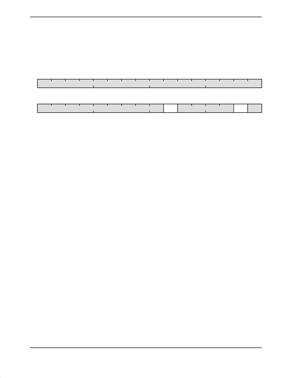
System Control
Register 5: Interrupt Mask Control (IMC), offset 0x054
Central location for system control interrupt masks.
Interrupt Mask Control (IMC)
Base 0x400F.E000
Offset 0x054
Type R/W, reset 0x0000.0000
reserved
DescriptionResetTypeNameBit/Field
16171819202122232425262728293031
ROROROROROROROROROROROROROROROROType
0000000000000000Reset
0123456789101112131415
reserved
BORIMreservedPLLLIMreserved
ROR/WROROROROR/WROROROROROROROROROType
0000000000000000Reset
0ROreserved31:7
Software should not rely on the value of a reserved bit. To provide
compatibility with future products, the value of a reserved bit should be
preserved across a read-modify-write operation.
0R/WPLLLIM6
PLL Lock Interrupt Mask
This bit specifies whether a PLL Lock interrupt is promoted to a controller
interrupt. If set, an interrupt is generated if PLLLRIS in RIS is set;
otherwise, an interrupt is not generated.
0ROreserved5:2
Software should not rely on the value of a reserved bit. To provide
compatibility with future products, the value of a reserved bit should be
preserved across a read-modify-write operation.
0R/WBORIM1
Brown-Out Reset Interrupt Mask
This bit specifies whether a brown-out condition is promoted to a
controller interrupt. If set, an interrupt is generated if BORRIS is set;
otherwise, an interrupt is not generated.
0ROreserved0
Software should not rely on the value of a reserved bit. To provide
compatibility with future products, the value of a reserved bit should be
preserved across a read-modify-write operation.
Texas Instruments-Production Data
June 23, 201080
Page 81

Register 6: Masked Interrupt Status and Clear (MISC), offset 0x058
On a read, this register gives the current masked status value of the corresponding interrupt. All of
the bits are R/W1C and this action also clears the corresponding raw interrupt bit in the RIS register
(see page 79).
Masked Interrupt Status and Clear (MISC)
Base 0x400F.E000
Offset 0x058
Type R/W1C, reset 0x0000.0000
reserved
DescriptionResetTypeNameBit/Field
Stellaris® LM3S1332 Microcontroller
16171819202122232425262728293031
ROROROROROROROROROROROROROROROROType
0000000000000000Reset
0123456789101112131415
BORMISreservedPLLLMISreserved
reserved
ROR/W1CROROROROR/W1CROROROROROROROROROType
0000000000000000Reset
0ROreserved31:7
Software should not rely on the value of a reserved bit. To provide
compatibility with future products, the value of a reserved bit should be
preserved across a read-modify-write operation.
0R/W1CPLLLMIS6
PLL Lock Masked Interrupt Status
This bit is set when the PLL T
READY
timer asserts. The interrupt is cleared
by writing a 1 to this bit.
0ROreserved5:2
Software should not rely on the value of a reserved bit. To provide
compatibility with future products, the value of a reserved bit should be
preserved across a read-modify-write operation.
0R/W1CBORMIS1
BOR Masked Interrupt Status
The BORMIS is simply the BORRIS ANDed with the mask value, BORIM.
0ROreserved0
Software should not rely on the value of a reserved bit. To provide
compatibility with future products, the value of a reserved bit should be
preserved across a read-modify-write operation.
Texas Instruments-Production Data
81June 23, 2010
Page 82
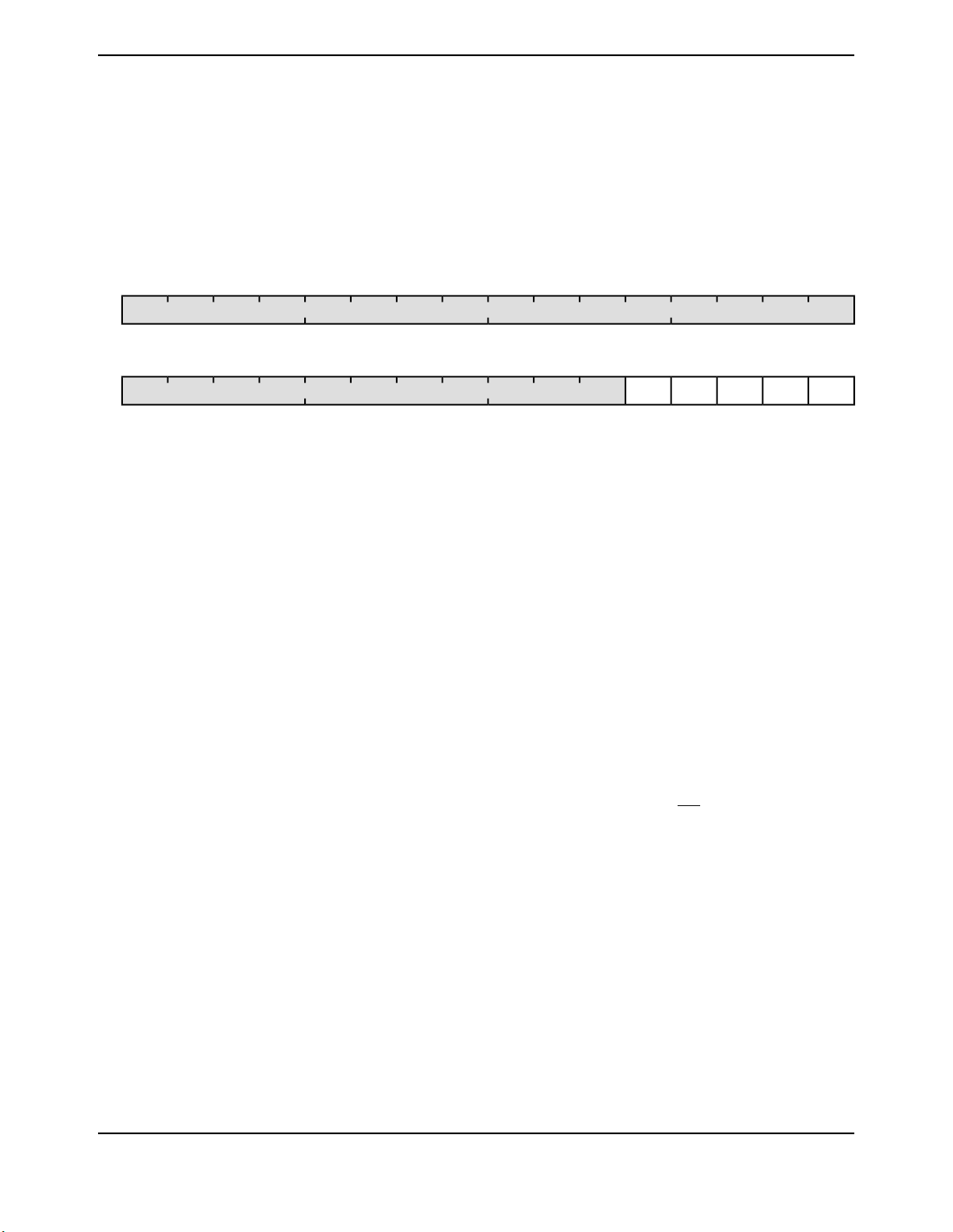
System Control
Register 7: Reset Cause (RESC), offset 0x05C
This register is set with the reset cause after reset. The bits in this register are sticky and maintain
their state across multiple reset sequences, except when an power-on reset is the cause, in which
case, all bits other than POR in the RESC register are cleared.
Reset Cause (RESC)
Base 0x400F.E000
Offset 0x05C
Type R/W, reset -
reserved
DescriptionResetTypeNameBit/Field
16171819202122232425262728293031
ROROROROROROROROROROROROROROROROType
0000000000000000Reset
0123456789101112131415
EXTPORBORWDTSWreserved
R/WR/WR/WR/WR/WROROROROROROROROROROROType
-----00000000000Reset
0ROreserved31:5
Software should not rely on the value of a reserved bit. To provide
compatibility with future products, the value of a reserved bit should be
preserved across a read-modify-write operation.
-R/WSW4
Software Reset
When set, indicates a software reset is the cause of the reset event.
-R/WWDT3
Watchdog Timer Reset
When set, indicates a watchdog reset is the cause of the reset event.
-R/WBOR2
Brown-Out Reset
When set, indicates a brown-out reset is the cause of the reset event.
-R/WPOR1
Power-On Reset
When set, indicates a power-on reset is the cause of the reset event.
-R/WEXT0
External Reset
When set, indicates an external reset (RST assertion) is the cause of
the reset event.
Texas Instruments-Production Data
June 23, 201082
Page 83
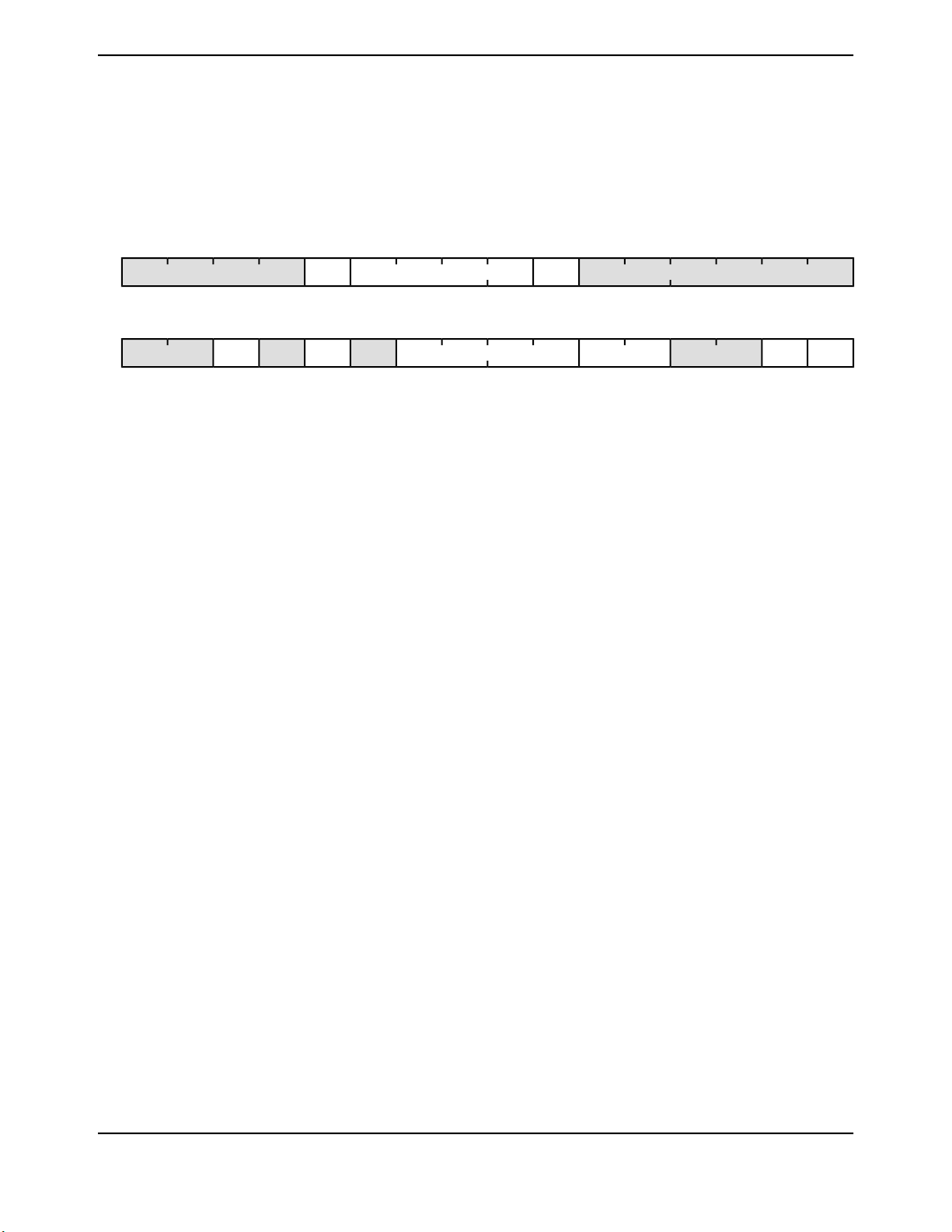
Register 8: Run-Mode Clock Configuration (RCC), offset 0x060
This register is defined to provide source control and frequency speed.
Run-Mode Clock Configuration (RCC)
Base 0x400F.E000
Offset 0x060
Type R/W, reset 0x0780.3AD1
reserved
PWRDNreserved
BYPASS
reserved
Stellaris® LM3S1332 Microcontroller
16171819202122232425262728293031
SYSDIVACGreserved
USESYSDIV
DescriptionResetTypeNameBit/Field
reserved
ROROROROROROR/WR/WR/WR/WR/WR/WROROROROType
0000000111100000Reset
0123456789101112131415
MOSCDISIOSCDISreservedOSCSRCXTAL
R/WR/WROROR/WR/WR/WR/WR/WR/WROR/WROR/WROROType
1000101101011100Reset
0x0ROreserved31:28
Software should not rely on the value of a reserved bit. To provide
compatibility with future products, the value of a reserved bit should be
preserved across a read-modify-write operation.
0R/WACG27
Auto Clock Gating
This bit specifies whether the system uses the Sleep-Mode Clock
Gating Control (SCGCn) registers and Deep-Sleep-Mode Clock
Gating Control (DCGCn) registers if the controller enters a Sleep or
Deep-Sleep mode (respectively). If set, the SCGCn or DCGCn registers
are used to control the clocks distributed to the peripherals when the
controller is in a sleep mode. Otherwise, the Run-Mode Clock Gating
Control (RCGCn) registers are used when the controller enters a sleep
mode.
The RCGCn registers are always used to control the clocks in Run
mode.
This allows peripherals to consume less power when the controller is
in a sleep mode and the peripheral is unused.
0xFR/WSYSDIV26:23
System Clock Divisor
Specifies which divisor is used to generate the system clock from either
the PLL output or the oscillator source (depending on how the BYPASS
bit in this register is configured). See Table 6-2 on page 69 for bit
encodings.
If the SYSDIV value is less than MINSYSDIV (see page 94), and the
PLL is being used, then the MINSYSDIV value is used as the divisor.
If the PLL is not being used, the SYSDIV value can be less than
MINSYSDIV.
0R/WUSESYSDIV22
Enable System Clock Divider
Use the system clock divider as the source for the system clock. The
system clock divider is forced to be used when the PLL is selected as
the source.
If the USERCC2 bit in the RCC2 register is set, then the SYSDIV2 field
in the RCC2 register is used as the system clock divider rather than the
SYSDIV field in this register.
Texas Instruments-Production Data
83June 23, 2010
Page 84

System Control
DescriptionResetTypeNameBit/Field
0ROreserved21:14
1R/WPWRDN13
1ROreserved12
1R/WBYPASS11
0ROreserved10
Software should not rely on the value of a reserved bit. To provide
compatibility with future products, the value of a reserved bit should be
preserved across a read-modify-write operation.
PLL Power Down
This bit connects to the PLL PWRDN input. The reset value of 1 powers
down the PLL.
Software should not rely on the value of a reserved bit. To provide
compatibility with future products, the value of a reserved bit should be
preserved across a read-modify-write operation.
PLL Bypass
Chooses whether the system clock is derived from the PLL output or
the OSC source. If set, the clock that drives the system is the OSC
source. Otherwise, the clock that drives the system is the PLL output
clock divided by the system divider.
See Table 6-2 on page 69 for programming guidelines.
Note: The ADC must be clocked from the PLL or directly from a
14-MHz to 18-MHz clock source to operate properly. While
the ADC works in a 14-18 MHz range, to maintain a 1 M
sample/second rate, the ADC must be provided a 16-MHz
clock source.
Software should not rely on the value of a reserved bit. To provide
compatibility with future products, the value of a reserved bit should be
preserved across a read-modify-write operation.
Texas Instruments-Production Data
June 23, 201084
Page 85

Stellaris® LM3S1332 Microcontroller
DescriptionResetTypeNameBit/Field
0xBR/WXTAL9:6
Crystal Value
This field specifies the crystal value attached to the main oscillator. The
encoding for this field is provided below. Depending on the crystal used,
the PLL frequency may not be exactly 400 MHz (see Table
19-9 on page 429 for more information).
Crystal Frequency (MHz) Not
Value
Using the PLL
6 MHz (reset value)0xB
Crystal Frequency (MHz) Using
the PLL
reserved1.0000x0
reserved1.84320x1
reserved2.0000x2
reserved2.45760x3
3.579545 MHz0x4
3.6864 MHz0x5
4 MHz0x6
4.096 MHz0x7
4.9152 MHz0x8
5 MHz0x9
5.12 MHz0xA
6.144 MHz0xC
7.3728 MHz0xD
8 MHz0xE
8.192 MHz0xF
0x1R/WOSCSRC5:4
0x0ROreserved3:2
Oscillator Source
Selects the input source for the OSC. The values are:
Input SourceValue
MOSC
0x0
Main oscillator
IOSC
0x1
Internal oscillator (default)
IOSC/4
0x2
Internal oscillator / 4
30 kHz
0x3
30-KHz internal oscillator
For additional oscillator sources, see the RCC2 register.
Software should not rely on the value of a reserved bit. To provide
compatibility with future products, the value of a reserved bit should be
preserved across a read-modify-write operation.
Texas Instruments-Production Data
85June 23, 2010
Page 86

System Control
DescriptionResetTypeNameBit/Field
0R/WIOSCDIS1
1R/WMOSCDIS0
Internal Oscillator Disable
0: Internal oscillator (IOSC) is enabled.
1: Internal oscillator is disabled.
Main Oscillator Disable
0: Main oscillator is enabled .
1: Main oscillator is disabled (default).
Texas Instruments-Production Data
June 23, 201086
Page 87
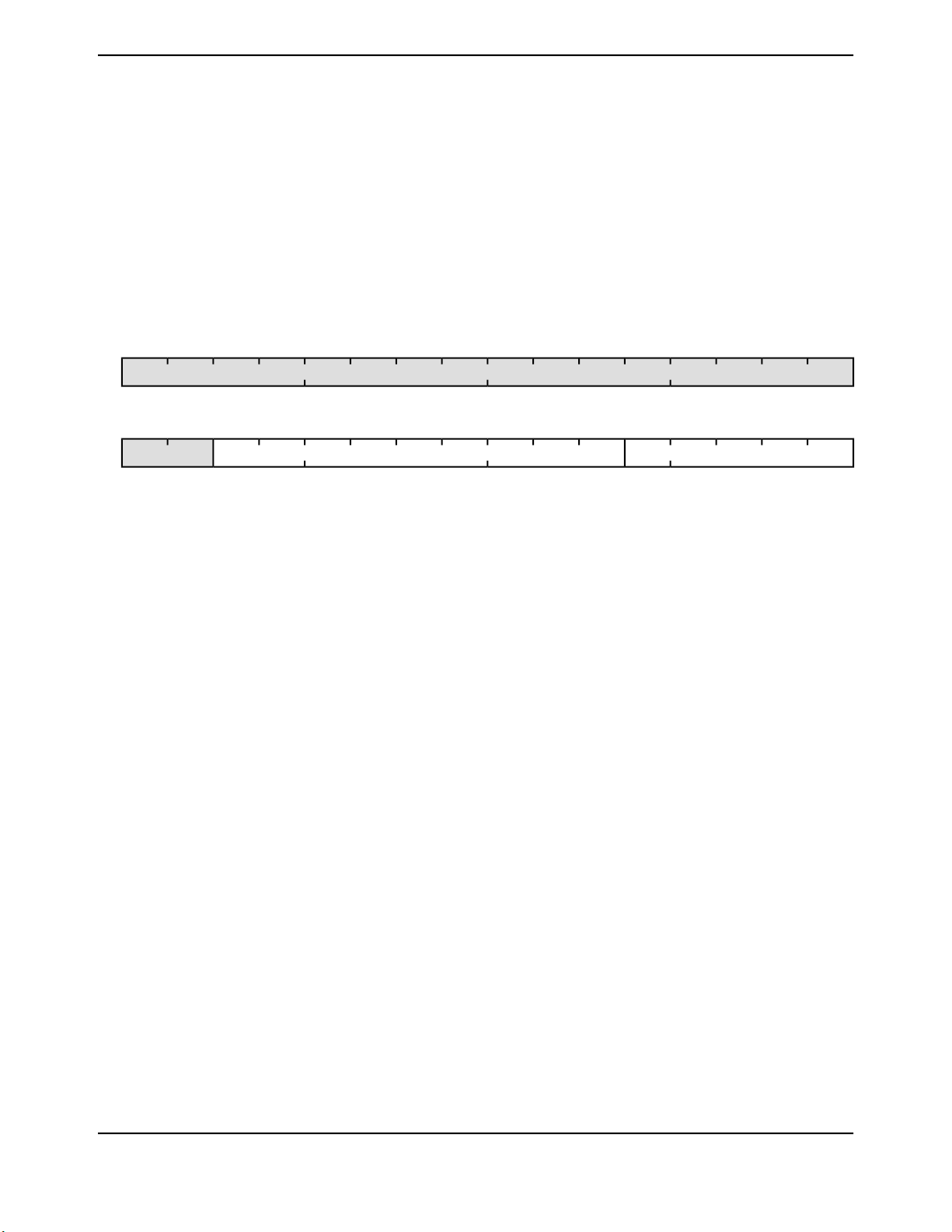
Register 9: XTAL to PLL Translation (PLLCFG), offset 0x064
This register provides a means of translating external crystal frequencies into the appropriate PLL
settings. This register is initialized during the reset sequence and updated anytime that the XTAL
field changes in the Run-Mode Clock Configuration (RCC) register (see page 83).
The PLL frequency is calculated using the PLLCFG field values, as follows:
PLLFreq = OSCFreq * F / (R + 1)
XTAL to PLL Translation (PLLCFG)
Base 0x400F.E000
Offset 0x064
Type RO, reset -
reserved
Stellaris® LM3S1332 Microcontroller
16171819202122232425262728293031
ROROROROROROROROROROROROROROROROType
0000000000000000Reset
0123456789101112131415
RFreserved
ROROROROROROROROROROROROROROROROType
--------------00Reset
DescriptionResetTypeNameBit/Field
0x0ROreserved31:14
Software should not rely on the value of a reserved bit. To provide
compatibility with future products, the value of a reserved bit should be
preserved across a read-modify-write operation.
-ROF13:5
PLL F Value
This field specifies the value supplied to the PLL’s F input.
-ROR4:0
PLL R Value
This field specifies the value supplied to the PLL’s R input.
Texas Instruments-Production Data
87June 23, 2010
Page 88
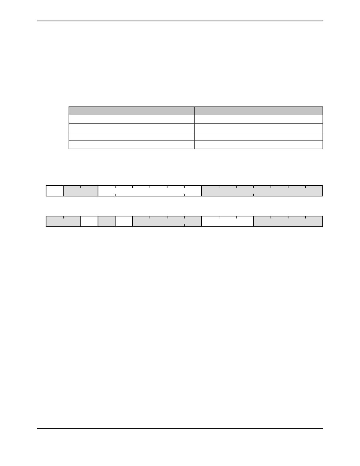
System Control
Register 10: Run-Mode Clock Configuration 2 (RCC2), offset 0x070
This register overrides the RCC equivalent register fields, as shown in Table 6-5, when the USERCC2
bit is set, allowing the extended capabilities of the RCC2 register to be used while also providing a
means to be backward-compatible to previous parts. Each RCC2 field that supersedes an RCC
field is located at the same LSB bit position; however, some RCC2 fields are larger than the
corresponding RCC field.
Table 6-5. RCC2 Fields that Override RCC fields
Run-Mode Clock Configuration 2 (RCC2)
Base 0x400F.E000
Offset 0x070
Type R/W, reset 0x0780.2810
PWRDN2reserved
reserved
Overrides RCC FieldRCC2 Field...
SYSDIV, bits[26:23]SYSDIV2, bits[28:23]
PWRDN, bit[13]PWRDN2, bit[13]
BYPASS, bit[11]BYPASS2, bit[11]
OSCSRC, bits[5:4]OSCSRC2, bits[6:4]
16171819202122232425262728293031
reservedSYSDIV2reservedUSERCC2
ROROROROROROROR/WR/WR/WR/WR/WR/WROROR/WType
0000000111100000Reset
0123456789101112131415
reservedOSCSRC2reservedBYPASS2
ROROROROR/WR/WR/WROROROROR/WROR/WROROType
0000100000010100Reset
DescriptionResetTypeNameBit/Field
0R/WUSERCC231
Use RCC2
When set, overrides the RCC register fields.
0x0ROreserved30:29
Software should not rely on the value of a reserved bit. To provide
compatibility with future products, the value of a reserved bit should be
preserved across a read-modify-write operation.
0x0FR/WSYSDIV228:23
System Clock Divisor
Specifies which divisor is used to generate the system clock from either
the PLL output or the oscillator source (depending on how the BYPASS2
bit is configured). SYSDIV2 is used for the divisor when both the
USESYSDIV bit in the RCC register and the USERCC2 bit in this register
are set. See Table 6-3 on page 69 for programming guidelines.
0x0ROreserved22:14
Software should not rely on the value of a reserved bit. To provide
compatibility with future products, the value of a reserved bit should be
preserved across a read-modify-write operation.
1R/WPWRDN213
Power-Down PLL
When set, powers down the PLL.
0ROreserved12
Software should not rely on the value of a reserved bit. To provide
compatibility with future products, the value of a reserved bit should be
preserved across a read-modify-write operation.
Texas Instruments-Production Data
June 23, 201088
Page 89

Stellaris® LM3S1332 Microcontroller
DescriptionResetTypeNameBit/Field
1R/WBYPASS211
0x0ROreserved10:7
0x1R/WOSCSRC26:4
Bypass PLL
When set, bypasses the PLL for the clock source.
See Table 6-3 on page 69 for programming guidelines.
Software should not rely on the value of a reserved bit. To provide
compatibility with future products, the value of a reserved bit should be
preserved across a read-modify-write operation.
Oscillator Source
Selects the input source for the OSC. The values are:
DescriptionValue
MOSC
0x0
Main oscillator
IOSC
0x1
Internal oscillator
IOSC/4
0x2
Internal oscillator / 4
30 kHz
0x3
30-kHz internal oscillator
Reserved0x4
Reserved0x5
Reserved0x6
32 kHz
0x7
32.768-kHz external oscillator
0ROreserved3:0
Software should not rely on the value of a reserved bit. To provide
compatibility with future products, the value of a reserved bit should be
preserved across a read-modify-write operation.
Texas Instruments-Production Data
89June 23, 2010
Page 90

System Control
Register 11: Deep Sleep Clock Configuration (DSLPCLKCFG), offset 0x144
This register provides configuration information for the hardware control of Deep Sleep Mode.
Deep Sleep Clock Configuration (DSLPCLKCFG)
Base 0x400F.E000
Offset 0x144
Type R/W, reset 0x0780.0000
16171819202122232425262728293031
reservedDSDIVORIDEreserved
ROROROROROROROR/WR/WR/WR/WR/WR/WROROROType
0000000111100000Reset
0123456789101112131415
reservedDSOSCSRCreserved
ROROROROR/WR/WR/WROROROROROROROROROType
0000000000000000Reset
DescriptionResetTypeNameBit/Field
0x0ROreserved31:29
Software should not rely on the value of a reserved bit. To provide
compatibility with future products, the value of a reserved bit should be
preserved across a read-modify-write operation.
0x0FR/WDSDIVORIDE28:23
Divider Field Override
6-bit system divider field to override when Deep-Sleep occurs with PLL
running.
0x0ROreserved22:7
Software should not rely on the value of a reserved bit. To provide
compatibility with future products, the value of a reserved bit should be
preserved across a read-modify-write operation.
0x0R/WDSOSCSRC6:4
Clock Source
Specifies the clock source during Deep-Sleep mode.
DescriptionValue
MOSC
0x0
Use main oscillator as source.
IOSC
0x1
Use internal 12-MHz oscillator as source.
Reserved0x2
30 kHz
0x3
Use 30-kHz internal oscillator as source.
Reserved0x4
Reserved0x5
Reserved0x6
32 kHz
0x7
Use 32.768-kHz external oscillator as source.
0x0ROreserved3:0
Software should not rely on the value of a reserved bit. To provide
compatibility with future products, the value of a reserved bit should be
preserved across a read-modify-write operation.
Texas Instruments-Production Data
June 23, 201090
Page 91

Register 12: Device Identification 1 (DID1), offset 0x004
This register identifies the device family, part number, temperature range, pin count, and package
type.
Device Identification 1 (DID1)
Base 0x400F.E000
Offset 0x004
Type RO, reset -
Stellaris® LM3S1332 Microcontroller
16171819202122232425262728293031
PARTNOFAMVER
ROROROROROROROROROROROROROROROROType
0110001100001000Reset
0123456789101112131415
QUALROHSPKGTEMPreservedPINCOUNT
ROROROROROROROROROROROROROROROROType
--1-----00000010Reset
DescriptionResetTypeNameBit/Field
0x1ROVER31:28
DID1 Version
This field defines the DID1 register format version. The version number
is numeric. The value of the VER field is encoded as follows (all other
encodings are reserved):
DescriptionValue
Second version of the DID1 register format.0x1
0x0ROFAM27:24
Family
This field provides the family identification of the device within the
Luminary Micro product portfolio. The value is encoded as follows (all
other encodings are reserved):
DescriptionValue
Stellaris family of microcontollers, that is, all devices with
0x0
external part numbers starting with LM3S.
0xC6ROPARTNO23:16
Part Number
This field provides the part number of the device within the family. The
value is encoded as follows (all other encodings are reserved):
DescriptionValue
LM3S13320xC6
0x2ROPINCOUNT15:13
Package Pin Count
This field specifies the number of pins on the device package. The value
is encoded as follows (all other encodings are reserved):
DescriptionValue
100-pin or 108-ball package0x2
Texas Instruments-Production Data
91June 23, 2010
Page 92

System Control
DescriptionResetTypeNameBit/Field
0ROreserved12:8
-ROTEMP7:5
-ROPKG4:3
1ROROHS2
Software should not rely on the value of a reserved bit. To provide
compatibility with future products, the value of a reserved bit should be
preserved across a read-modify-write operation.
Temperature Range
This field specifies the temperature rating of the device. The value is
encoded as follows (all other encodings are reserved):
DescriptionValue
Commercial temperature range (0°C to 70°C)0x0
Industrial temperature range (-40°C to 85°C)0x1
Extended temperature range (-40°C to 105°C)0x2
Package Type
This field specifies the package type. The value is encoded as follows
(all other encodings are reserved):
DescriptionValue
SOIC package0x0
LQFP package0x1
BGA package0x2
RoHS-Compliance
This bit specifies whether the device is RoHS-compliant. A 1 indicates
the part is RoHS-compliant.
-ROQUAL1:0
Qualification Status
This field specifies the qualification status of the device. The value is
encoded as follows (all other encodings are reserved):
DescriptionValue
Engineering Sample (unqualified)0x0
Pilot Production (unqualified)0x1
Fully Qualified0x2
Texas Instruments-Production Data
June 23, 201092
Page 93

Register 13: Device Capabilities 0 (DC0), offset 0x008
This register is predefined by the part and can be used to verify features.
Device Capabilities 0 (DC0)
Base 0x400F.E000
Offset 0x008
Type RO, reset 0x003F.002F
SRAMSZ
FLASHSZ
DescriptionResetTypeNameBit/Field
Stellaris® LM3S1332 Microcontroller
16171819202122232425262728293031
ROROROROROROROROROROROROROROROROType
1111110000000000Reset
0123456789101112131415
ROROROROROROROROROROROROROROROROType
1111010000000000Reset
0x003FROSRAMSZ31:16
SRAM Size
Indicates the size of the on-chip SRAM memory.
DescriptionValue
16 KB of SRAM0x003F
0x002FROFLASHSZ15:0
Flash Size
Indicates the size of the on-chip flash memory.
DescriptionValue
96 KB of Flash0x002F
Texas Instruments-Production Data
93June 23, 2010
Page 94

System Control
Register 14: Device Capabilities 1 (DC1), offset 0x010
This register provides a list of features available in the system. The Stellaris family uses this register
format to indicate the availability of the following family features in the specific device: CANs, PWM,
ADC, Watchdog timer, Hibernation module, and debug capabilities. This register also indicates the
maximum clock frequency and maximum ADC sample rate. The format of this register is consistent
with the RCGC0, SCGC0, and DCGC0 clock control registers and the SRCR0 software reset control
register.
Device Capabilities 1 (DC1)
Base 0x400F.E000
Offset 0x010
Type RO, reset 0x0001.31FF
16171819202122232425262728293031
ADCreserved
ROROROROROROROROROROROROROROROROType
1000000000000000Reset
0123456789101112131415
JTAGSWDSWOWDTPLLTEMPSNSHIBMPUMAXADCSPDreservedMINSYSDIV
ROROROROROROROROROROROROROROROROType
1111111110001100Reset
DescriptionResetTypeNameBit/Field
0ROreserved31:17
1ROADC16
0x3ROMINSYSDIV15:12
0ROreserved11:10
0x1ROMAXADCSPD9:8
Software should not rely on the value of a reserved bit. To provide
compatibility with future products, the value of a reserved bit should be
preserved across a read-modify-write operation.
ADC Module Present
When set, indicates that the ADC module is present.
System Clock Divider
Minimum 4-bit divider value for system clock. The reset value is
hardware-dependent. See the RCC register for how to change the
system clock divisor using the SYSDIV bit.
DescriptionValue
Specifies a 50-MHz CPU clock with a PLL divider of 4.0x3
Software should not rely on the value of a reserved bit. To provide
compatibility with future products, the value of a reserved bit should be
preserved across a read-modify-write operation.
Max ADC Speed
Indicates the maximum rate at which the ADC samples data.
DescriptionValue
250K samples/second0x1
1ROMPU7
MPU Present
When set, indicates that the Cortex-M3 Memory Protection Unit (MPU)
module is present. See the ARM Cortex-M3 Technical Reference Manual
for details on the MPU.
Texas Instruments-Production Data
June 23, 201094
Page 95

Stellaris® LM3S1332 Microcontroller
DescriptionResetTypeNameBit/Field
1ROHIB6
1ROTEMPSNS5
1ROPLL4
1ROWDT3
1ROSWO2
1ROSWD1
1ROJTAG0
Hibernation Module Present
When set, indicates that the Hibernation module is present.
Temp Sensor Present
When set, indicates that the on-chip temperature sensor is present.
PLL Present
When set, indicates that the on-chip Phase Locked Loop (PLL) is
present.
Watchdog Timer Present
When set, indicates that a watchdog timer is present.
SWO Trace Port Present
When set, indicates that the Serial Wire Output (SWO) trace port is
present.
SWD Present
When set, indicates that the Serial Wire Debugger (SWD) is present.
JTAG Present
When set, indicates that the JTAG debugger interface is present.
Texas Instruments-Production Data
95June 23, 2010
Page 96
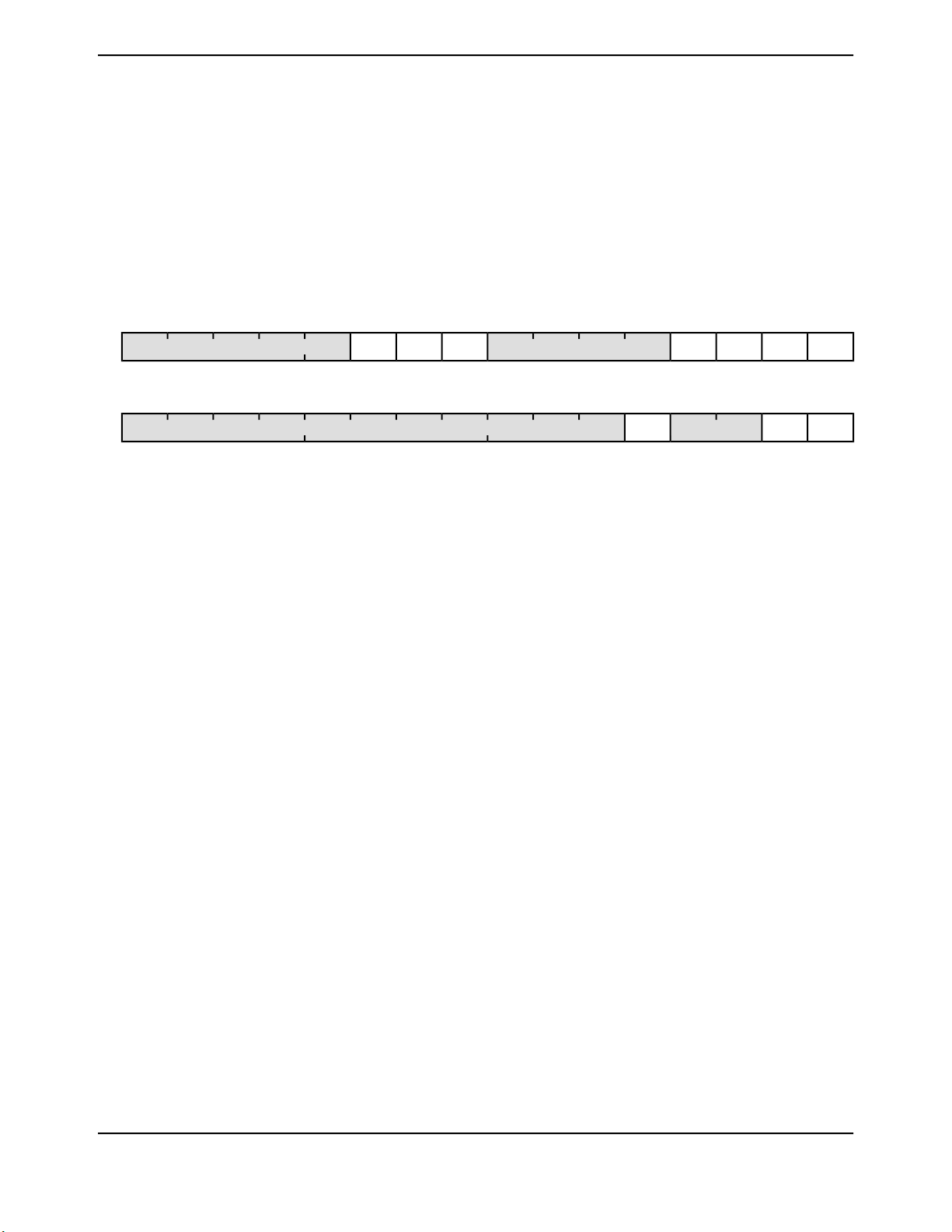
System Control
Register 15: Device Capabilities 2 (DC2), offset 0x014
This register provides a list of features available in the system. The Stellaris family uses this register
format to indicate the availability of the following family features in the specific device: Analog
Comparators, General-Purpose Timers, I2Cs, QEIs, SSIs, and UARTs. The format of this register
is consistent with the RCGC1, SCGC1, and DCGC1 clock control registers and the SRCR1 software
reset control register.
Device Capabilities 2 (DC2)
Base 0x400F.E000
Offset 0x014
Type RO, reset 0x070F.0013
16171819202122232425262728293031
TIMER0TIMER1TIMER2TIMER3reservedCOMP0COMP1COMP2reserved
ROROROROROROROROROROROROROROROROType
1111000011100000Reset
0123456789101112131415
UART0UART1reservedSSI0reserved
ROROROROROROROROROROROROROROROROType
1100100000000000Reset
DescriptionResetTypeNameBit/Field
0ROreserved31:27
Software should not rely on the value of a reserved bit. To provide
compatibility with future products, the value of a reserved bit should be
preserved across a read-modify-write operation.
1ROCOMP226
Analog Comparator 2 Present
When set, indicates that analog comparator 2 is present.
1ROCOMP125
Analog Comparator 1 Present
When set, indicates that analog comparator 1 is present.
1ROCOMP024
Analog Comparator 0 Present
When set, indicates that analog comparator 0 is present.
0ROreserved23:20
Software should not rely on the value of a reserved bit. To provide
compatibility with future products, the value of a reserved bit should be
preserved across a read-modify-write operation.
1ROTIMER319
Timer 3 Present
When set, indicates that General-Purpose Timer module 3 is present.
1ROTIMER218
Timer 2 Present
When set, indicates that General-Purpose Timer module 2 is present.
1ROTIMER117
Timer 1 Present
When set, indicates that General-Purpose Timer module 1 is present.
1ROTIMER016
Timer 0 Present
When set, indicates that General-Purpose Timer module 0 is present.
0ROreserved15:5
Software should not rely on the value of a reserved bit. To provide
compatibility with future products, the value of a reserved bit should be
preserved across a read-modify-write operation.
Texas Instruments-Production Data
June 23, 201096
Page 97

Stellaris® LM3S1332 Microcontroller
DescriptionResetTypeNameBit/Field
1ROSSI04
0ROreserved3:2
1ROUART11
1ROUART00
SSI0 Present
When set, indicates that SSI module 0 is present.
Software should not rely on the value of a reserved bit. To provide
compatibility with future products, the value of a reserved bit should be
preserved across a read-modify-write operation.
UART1 Present
When set, indicates that UART module 1 is present.
UART0 Present
When set, indicates that UART module 0 is present.
Texas Instruments-Production Data
97June 23, 2010
Page 98
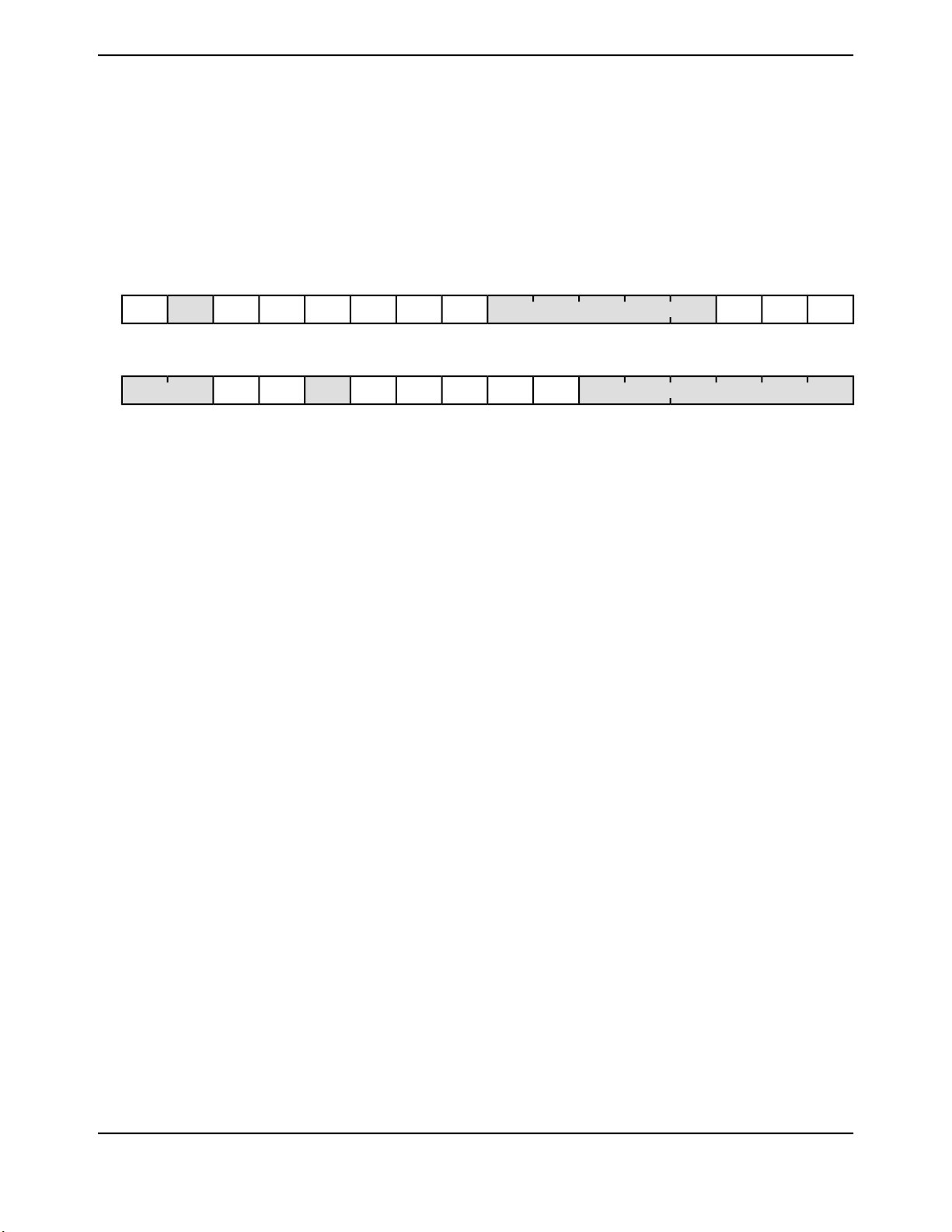
System Control
Register 16: Device Capabilities 3 (DC3), offset 0x018
This register provides a list of features available in the system. The Stellaris family uses this register
format to indicate the availability of the following family features in the specific device: Analog
Comparator I/Os, CCP I/Os, ADC I/Os, and PWM I/Os.
Device Capabilities 3 (DC3)
Base 0x400F.E000
Offset 0x018
Type RO, reset 0xBF07.37C0
reserved
32KHZ
16171819202122232425262728293031
ADC0ADC1ADC2reservedCCP0CCP1CCP2CCP3CCP4CCP5
ROROROROROROROROROROROROROROROROType
1110000011111101Reset
0123456789101112131415
C2MINUSC2PLUSreserved
reserved
reservedC0MINUSC0PLUSC0OC1MINUSC1PLUS
ROROROROROROROROROROROROROROROROType
0000001111101100Reset
DescriptionResetTypeNameBit/Field
1RO32KHZ31
32KHz Input Clock Available
When set, indicates an even CCP pin is present and can be used as a
32-KHz input clock.
0ROreserved30
Software should not rely on the value of a reserved bit. To provide
compatibility with future products, the value of a reserved bit should be
preserved across a read-modify-write operation.
1ROCCP529
CCP5 Pin Present
When set, indicates that Capture/Compare/PWM pin 5 is present.
1ROCCP428
CCP4 Pin Present
When set, indicates that Capture/Compare/PWM pin 4 is present.
1ROCCP327
CCP3 Pin Present
When set, indicates that Capture/Compare/PWM pin 3 is present.
1ROCCP226
CCP2 Pin Present
When set, indicates that Capture/Compare/PWM pin 2 is present.
1ROCCP125
CCP1 Pin Present
When set, indicates that Capture/Compare/PWM pin 1 is present.
1ROCCP024
CCP0 Pin Present
When set, indicates that Capture/Compare/PWM pin 0 is present.
0ROreserved23:19
Software should not rely on the value of a reserved bit. To provide
compatibility with future products, the value of a reserved bit should be
preserved across a read-modify-write operation.
1ROADC218
ADC2 Pin Present
When set, indicates that ADC pin 2 is present.
Texas Instruments-Production Data
June 23, 201098
Page 99

Stellaris® LM3S1332 Microcontroller
DescriptionResetTypeNameBit/Field
1ROADC117
1ROADC016
0ROreserved15:14
1ROC2PLUS13
1ROC2MINUS12
0ROreserved11
1ROC1PLUS10
1ROC1MINUS9
ADC1 Pin Present
When set, indicates that ADC pin 1 is present.
ADC0 Pin Present
When set, indicates that ADC pin 0 is present.
Software should not rely on the value of a reserved bit. To provide
compatibility with future products, the value of a reserved bit should be
preserved across a read-modify-write operation.
C2+ Pin Present
When set, indicates that the analog comparator 2 (+) input pin is present.
C2- Pin Present
When set, indicates that the analog comparator 2 (-) input pin is present.
Software should not rely on the value of a reserved bit. To provide
compatibility with future products, the value of a reserved bit should be
preserved across a read-modify-write operation.
C1+ Pin Present
When set, indicates that the analog comparator 1 (+) input pin is present.
C1- Pin Present
When set, indicates that the analog comparator 1 (-) input pin is present.
1ROC0O8
1ROC0PLUS7
1ROC0MINUS6
0ROreserved5:0
C0o Pin Present
When set, indicates that the analog comparator 0 output pin is present.
C0+ Pin Present
When set, indicates that the analog comparator 0 (+) input pin is present.
C0- Pin Present
When set, indicates that the analog comparator 0 (-) input pin is present.
Software should not rely on the value of a reserved bit. To provide
compatibility with future products, the value of a reserved bit should be
preserved across a read-modify-write operation.
Texas Instruments-Production Data
99June 23, 2010
Page 100

System Control
Register 17: Device Capabilities 4 (DC4), offset 0x01C
This register provides a list of features available in the system. The Stellaris family uses this register
format to indicate the availability of the following family features in the specific device: Ethernet MAC
and PHY, GPIOs, and CCP I/Os. The format of this register is consistent with the RCGC2, SCGC2,
and DCGC2 clock control registers and the SRCR2 software reset control register.
Device Capabilities 4 (DC4)
Base 0x400F.E000
Offset 0x01C
Type RO, reset 0x0000.C0FF
reserved
DescriptionResetTypeNameBit/Field
16171819202122232425262728293031
ROROROROROROROROROROROROROROROROType
0000000000000000Reset
0123456789101112131415
GPIOAGPIOBGPIOCGPIODGPIOEGPIOFGPIOGGPIOHreservedCCP6CCP7
ROROROROROROROROROROROROROROROROType
1111111100000011Reset
0ROreserved31:16
Software should not rely on the value of a reserved bit. To provide
compatibility with future products, the value of a reserved bit should be
preserved across a read-modify-write operation.
1ROCCP715
CCP7 Pin Present
When set, indicates that Capture/Compare/PWM pin 7 is present.
1ROCCP614
CCP6 Pin Present
When set, indicates that Capture/Compare/PWM pin 6 is present.
0ROreserved13:8
Software should not rely on the value of a reserved bit. To provide
compatibility with future products, the value of a reserved bit should be
preserved across a read-modify-write operation.
1ROGPIOH7
GPIO Port H Present
When set, indicates that GPIO Port H is present.
1ROGPIOG6
GPIO Port G Present
When set, indicates that GPIO Port G is present.
1ROGPIOF5
GPIO Port F Present
When set, indicates that GPIO Port F is present.
1ROGPIOE4
GPIO Port E Present
When set, indicates that GPIO Port E is present.
1ROGPIOD3
GPIO Port D Present
When set, indicates that GPIO Port D is present.
1ROGPIOC2
GPIO Port C Present
When set, indicates that GPIO Port C is present.
Texas Instruments-Production Data
June 23, 2010100
 Loading...