

Page 1

User’s Guide
July 2004
SBAU096
Page 2

IMPORTANT NOTICE
Texas Instruments Incorporated and its subsidiaries (TI) reserve the right to make corrections, modifications,
enhancements, improvements, and other changes to its products and services at any time and to discontinue
any product or service without notice. Customers should obtain the latest relevant information before placing
orders and should verify that such information is current and complete. All products are sold subject to TI’s terms
and conditions of sale supplied at the time of order acknowledgment.
TI warrants performance of its hardware products to the specifications applicable at the time of sale in
accordance with TI’s standard warranty. Testing and other quality control techniques are used to the extent TI
deems necessary to support this warranty . Except where mandated by government requirements, testing of all
parameters of each product is not necessarily performed.
TI assumes no liability for applications assistance or customer product design. Customers are responsible for
their products and applications using TI components. To minimize the risks associated with customer products
and applications, customers should provide adequate design and operating safeguards.
TI does not warrant or represent that any license, either express or implied, is granted under any TI patent right,
copyright, mask work right, or other TI intellectual property right relating to any combination, machine, or process
in which TI products or services are used. Information published by TI regarding third-party products or services
does not constitute a license from TI to use such products or services or a warranty or endorsement thereof.
Use of such information may require a license from a third party under the patents or other intellectual property
of the third party, or a license from TI under the patents or other intellectual property of TI.
Reproduction of information in TI data books or data sheets is permissible only if reproduction is without
alteration and is accompanied by all associated warranties, conditions, limitations, and notices. Reproduction
of this information with alteration is an unfair and deceptive business practice. TI is not responsible or liable for
such altered documentation.
Resale of TI products or services with statements different from or beyond the parameters stated by TI for that
product or service voids all express and any implied warranties for the associated TI product or service and
is an unfair and deceptive business practice. TI is not responsible or liable for any such statements.
Following are URLs where you can obtain information on other Texas Instruments products and application
solutions:
Products Applications
Amplifiers amplifier.ti.com Audio www.ti.com/audio
Data Converters dataconverter.ti.com Automotive www.ti.com/automotive
DSP dsp.ti.com Broadband www.ti.com/broadband
Interface interface.ti.com Digital Control www.ti.com/digitalcontrol
Logic logic.ti.com Military www.ti.com/military
Power Mgmt power.ti.com Optical Networking www.ti.com/opticalnetwork
Microcontrollers microcontroller.ti.com Security www.ti.com/security
Telephony www.ti.com/telephony
Video & Imaging www.ti.com/video
Wireless www.ti.com/wireless
Mailing Address: Texas Instruments
Post Office Box 655303 Dallas, Texas 75265
Copyright 2004, Texas Instruments Incorporated
Page 3

EVM IMPORTANT NOTICE
Texas Instruments (TI) provides the enclosed product(s) under the following conditions:
This evaluation kit being sold by TI is intended for use for ENGINEERING DEVELOPMENT OR EVALUATION
PURPOSES ONLY and is not considered by TI to be fit for commercial use. As such, the goods being provided
may not be complete in terms of required design-, marketing-, and/or manufacturing-related protective
considerations, including product safety measures typically found in the end product incorporating the goods.
As a prototype, this product does not fall within the scope of the European Union directive on electromagnetic
compatibility and therefore may not meet the technical requirements of the directive.
Should this evaluation kit not meet the specifications indicated in the EVM User’s Guide, the kit may be returned
within 30 days from the date of delivery for a full refund. THE FOREGOING WARRANTY IS THE EXCLUSIVE
WARRANTY MADE BY SELLER TO BUYER AND IS IN LIEU OF ALL OTHER WARRANTIES, EXPRESSED,
IMPLIED, OR S TATUTORY, INCLUDING ANY WARRANTY OF MERCHANTABILITY OR FITNESS FOR ANY
PARTICULAR PURPOSE.
The user assumes all responsibility and liability for proper and safe handling of the goods. Further, the user
indemnifies TI from all claims arising from the handling or use of the goods. Please be aware that the products
received may not be regulatory compliant or agency certified (FCC, UL, CE, etc.). Due to the open construction
of the product, it is the user’s responsibility to take any and all appropriate precautions with regard to electrostatic
discharge.
EXCEPT TO THE EXTENT OF THE INDEMNITY SET FORTH ABOVE, NEITHER PARTY SHALL BE LIABLE
TO THE OTHER FOR ANY INDIRECT, SPECIAL, INCIDENTAL, OR CONSEQUENTIAL DAMAGES.
TI currently deals with a variety of customers for products, and therefore our arrangement with the user is not
exclusive.
TI assumes no liability for applications assistance, customer product design, software performance, or
infringement of patents or services described herein.
Please read the EVM User’s Guide and, specifically, the EVM Warnings and Restrictions notice in the EVM
User’s Guide prior to handling the product. This notice contains important safety information about temperatures
and voltages. For further safety concerns, please contact the TI application engineer.
Persons handling the product must have electronics training and observe good laboratory practice standards.
No license is granted under any patent right or other intellectual property right of TI covering or relating to any
machine, process, or combination in which such TI products or services might be or are used.
Mailing Address:
Texas Instruments
Post Office Box 655303
Dallas, Texas 75265
Copyright 2004, Texas Instruments Incorporated
Page 4

EVM WARNINGS AND RESTRICTIONS
It is important to operate this EVM within the absolute operating conditions shown in
Table 2−1.
Exceeding the specified input range may cause unexpected operation and/or irreversible
damage to the EVM. If there are questions concerning the input range, please contact a TI
field representative prior to connecting the input power.
Applying loads outside of the specified output range may result in unintended operation and/or
possible permanent damage to the EVM. Please consult the EVM User’s Guide prior to
connecting any load to the EVM output. If there is uncertainty as to the load specification,
please contact a TI field representative.
During normal operation, some circuit components may have case temperatures greater than
+70°C. The EVM is designed to operate properly with certain components above +70°C as
long as the input and output ranges are maintained. These components include but are not
limited to linear regulators, switching transistors, pass transistors, and current sense
resistors. These types of devices can be identified using the EVM schematic located in the
EVM User’s Guide. When placing measurement probes near these devices during operation,
please be aware that these devices may be very warm to the touch.
Mailing Address:
Texas Instruments
Post Office Box 655303
Dallas, Texas 75265
Copyright 2004, Texas Instruments Incorporated
Page 5

About This Manual
Contents
Preface
This document contains the information required to setup and operate the
SRC4194EVM evaluation module. For a more detailed description of the
SRC4194, please refer to the product datasheet available from the Texas Instruments web site at http://www.ti.com
listed in the sections of this guide entitled Related Documentation from Tex-
as Instruments and Additional Documentation.
. Additional support documents are
How to Use This Manual
Throughout this document, the term EVM and the phrase evaluation module
are synonymous with the SRC4194EVM.
Chapter 1 provides a product overview for the SRC4194 four-channel asynchronous sample rate converter. The SRC4194EVM block diagram and primary features are also discussed.
Chapter 2 provides general information regarding EVM handling and unpacking, as well as absolute operating conditions for power supplies and input/output connections.
Chapter 3 provides general hardware descriptions and configuration information for the EVM. The information in this chapter is designed to guide the user
in the setup of the EVM.
Chapter 4 includes the EVM electrical schematic, printed circuit board (PCB)
layout, and the bill of materials
Contents
iii
Page 6

Contents
Information About Cautions
This document contains cautions. The information in a caution is provided for
your protection. Please read each caution carefully.
This is an example of a caution statement.
A caution statement describes a situation that could potentially
damage your software or equipment.
iv
Page 7

Related Documentation From Texas Instruments
The following documents provide information regarding T exas Instrument integrated circuits used in the assembly of the SRC4194EVM. These documents
are available from the TI web site at http://www.ti.com
the literature number corresponds to the document revision, which is current
at the time of the writing of this User’s Guide. Newer revisions may be available
from the TI web site, or by calling the Texas Instruments Literature Response
Center at (800) 477−8924 or the Product Information Center at (972)
644−5580. When ordering, identify the document(s) by both title and literature
number.
Data Sheets: Literature Number:
SRC4194 SBFS025A
DIT4192 SBOS229B
PLL1705 SLES046A
REG1117 SBVS001B
SN74ALVC125 SCES110E
Contents
. The last character of
SN74ALVC244 SCES188B
SN74ALVC245 SCES271B
SN74LVC1G04 SCES214M
SN74LVC1G08 SCES217L
SN74LVC244A SCAS414U
Additional Documentation
The following documents or references provide information regarding selected non-TI components used in the assembly of the SRC4194EVM. These
documents are available from the corresponding manufacturer.
Document: Manufacturer:
CS8414 Data Sheet Cirrus Logic, web site: http://www.cirrus.com
HCM49 Series Crystals Citizen, web site: http://www.citizencrystals.com
Contents
v
Page 8

Contents
If You Need Assistance
If you have questions regarding either the use of this evaluation module or the
information contained in the accompanying documentation, please contact
the Texas Instruments Product Information Center at (972) 644−5580 or visit
the TI Semiconductor Online Technical Support pages at http://www.ti.com
FCC Warning
This equipment is intended for use in a laboratory test environment only. It may
generate, use, or radiate radio frequency energy and has not been tested for
compliance with the limits of computing devices pursuant to sub−part J of part
15 of the FCC regulations, which are designed to provide reasonable protection against radio frequency interference. Operation of this equipment in other
environments may cause interference with radio communications, in which
case the user at his own expense will be required to take whatever measures
may be required to correct this interference.
Trademarks
All trademarks are the property of their respective owners.
.
vi
Page 9

Contents
1 Introduction 1-1 . . . . . . . . . . . . . . . . . . . . . . . . . . . . . . . . . . . . . . . . . . . . . . . . . . . . . . . . . . . . . . . . . . . . .
1.1 SRC4194 Product Overview 1-2 . . . . . . . . . . . . . . . . . . . . . . . . . . . . . . . . . . . . . . . . . . . . . . . . .
1.2 SRC4194 Functional Block Diagram 1-3 . . . . . . . . . . . . . . . . . . . . . . . . . . . . . . . . . . . . . . . . . .
1.3 SRC4194EVM Features 1-5 . . . . . . . . . . . . . . . . . . . . . . . . . . . . . . . . . . . . . . . . . . . . . . . . . . . . .
1.4 SRC4194EVM Functional Block Diagram 1-6 . . . . . . . . . . . . . . . . . . . . . . . . . . . . . . . . . . . . . .
2 Getting Started 2-1 . . . . . . . . . . . . . . . . . . . . . . . . . . . . . . . . . . . . . . . . . . . . . . . . . . . . . . . . . . . . . . . . . .
2.1 Electrostatic Discharge Warning 2-2 . . . . . . . . . . . . . . . . . . . . . . . . . . . . . . . . . . . . . . . . . . . . . .
2.2 Unpacking the EVM 2-3 . . . . . . . . . . . . . . . . . . . . . . . . . . . . . . . . . . . . . . . . . . . . . . . . . . . . . . . .
2.3 Absolute Maximum Operating Conditions 2-4 . . . . . . . . . . . . . . . . . . . . . . . . . . . . . . . . . . . . .
3 Hardware Description and Configuration 3-1 . . . . . . . . . . . . . . . . . . . . . . . . . . . . . . . . . . . . . . . . . .
3.1 Power Supply Configuration 3-2 . . . . . . . . . . . . . . . . . . . . . . . . . . . . . . . . . . . . . . . . . . . . . . . . . .
3.2 SRC4194 Configuration Modes 3-4 . . . . . . . . . . . . . . . . . . . . . . . . . . . . . . . . . . . . . . . . . . . . . .
3.2.1 SRC4194 Hardware (or Standalone) Mode Configuration 3-4 . . . . . . . . . . . . . . . . .
3.2.2 SRC4194 Software Mode Configuration Via The Host Port 3-6 . . . . . . . . . . . . . . . .
3.3 Audio Input Ports 3-7 . . . . . . . . . . . . . . . . . . . . . . . . . . . . . . . . . . . . . . . . . . . . . . . . . . . . . . . . . . .
3.4 Audio Output Ports 3-8 . . . . . . . . . . . . . . . . . . . . . . . . . . . . . . . . . . . . . . . . . . . . . . . . . . . . . . . . .
3.5 Reference Clock Generation 3-10 . . . . . . . . . . . . . . . . . . . . . . . . . . . . . . . . . . . . . . . . . . . . . . . .
3.6 TDM Test Mode 3-11 . . . . . . . . . . . . . . . . . . . . . . . . . . . . . . . . . . . . . . . . . . . . . . . . . . . . . . . . . . .
4 Schematic, PCB Layout, and Bill of Materials 4-1 . . . . . . . . . . . . . . . . . . . . . . . . . . . . . . . . . . . . . .
4.1 Schematic 4-2 . . . . . . . . . . . . . . . . . . . . . . . . . . . . . . . . . . . . . . . . . . . . . . . . . . . . . . . . . . . . . . . . .
4.2 PCB Layout 4-5 . . . . . . . . . . . . . . . . . . . . . . . . . . . . . . . . . . . . . . . . . . . . . . . . . . . . . . . . . . . . . . . .
4.3 Bill of Materials 4-11 . . . . . . . . . . . . . . . . . . . . . . . . . . . . . . . . . . . . . . . . . . . . . . . . . . . . . . . . . . . .
Contents
vii
Page 10

Contents
1−1. SRC4194 Functional Block Diagram 1-4 . . . . . . . . . . . . . . . . . . . . . . . . . . . . . . . . . . . . . . . . . . . . .
1−2. SRC4194EVM Functional Block Diagram 1-6 . . . . . . . . . . . . . . . . . . . . . . . . . . . . . . . . . . . . . . . .
3−1. SRC4194EVM Power Supply Configuration and Jumpers 3-2 . . . . . . . . . . . . . . . . . . . . . . . . . .
3−2. Input Port External Connections and Configuration 3-7 . . . . . . . . . . . . . . . . . . . . . . . . . . . . . . . .
3−3. Output Port External Connections and Configuration 3-8 . . . . . . . . . . . . . . . . . . . . . . . . . . . . . . .
3−4. Reference Clock Generation, Connections, and Configuration 3-10 . . . . . . . . . . . . . . . . . . . . .
4−1. SRC4194EVM Schematic Diagram, Page 1 of 2 4-3 . . . . . . . . . . . . . . . . . . . . . . . . . . . . . . . . . .
4−2. SRC4194EVM Schematic Diagram, Page 2 of 2 4-4 . . . . . . . . . . . . . . . . . . . . . . . . . . . . . . . . . .
4−3. Top Side Silk Screen 4-5 . . . . . . . . . . . . . . . . . . . . . . . . . . . . . . . . . . . . . . . . . . . . . . . . . . . . . . . . . .
4−4. Bottom Side Silk Screen 4-6 . . . . . . . . . . . . . . . . . . . . . . . . . . . . . . . . . . . . . . . . . . . . . . . . . . . . . . .
4−5. Top Layer (Component Side) 4-7 . . . . . . . . . . . . . . . . . . . . . . . . . . . . . . . . . . . . . . . . . . . . . . . . . . .
4−6. Ground Plane Layer 4-8 . . . . . . . . . . . . . . . . . . . . . . . . . . . . . . . . . . . . . . . . . . . . . . . . . . . . . . . . . . .
4−7. Power Layer 4-9 . . . . . . . . . . . . . . . . . . . . . . . . . . . . . . . . . . . . . . . . . . . . . . . . . . . . . . . . . . . . . . . . . .
4−8. Bottom layer (Solder Side) 4-10 . . . . . . . . . . . . . . . . . . . . . . . . . . . . . . . . . . . . . . . . . . . . . . . . . . . .
2−1. Absolute Operating Conditions 2-4 . . . . . . . . . . . . . . . . . . . . . . . . . . . . . . . . . . . . . . . . . . . . . . . . . .
3−1. Common Configurations using a +5V Supply and an Optional EXT VIO Supply 3-3 . . . . . . . .
3−2. Setting the Configuration Mode 3-4 . . . . . . . . . . . . . . . . . . . . . . . . . . . . . . . . . . . . . . . . . . . . . . . . .
3−3. Hardware Mode Setup Matrix Using Switches SW1, SW2, SW4 and SW5 (x = A or B) 3-5
3−4. Transmitter Clock Divider Configuration 3-9 . . . . . . . . . . . . . . . . . . . . . . . . . . . . . . . . . . . . . . . . . .
3−5. Transmitter Stereo/Mono Mode Configuration 3-9 . . . . . . . . . . . . . . . . . . . . . . . . . . . . . . . . . . . . .
3−6. PLL Configuration for U25 and U28 3-10 . . . . . . . . . . . . . . . . . . . . . . . . . . . . . . . . . . . . . . . . . . . . .
4−1. Bill of Materials 4-11 . . . . . . . . . . . . . . . . . . . . . . . . . . . . . . . . . . . . . . . . . . . . . . . . . . . . . . . . . . . . . .
viii
Page 11

Chapter 1
This chapter provides a brief technical overview for the SRC4194 four-channel
audio asynchronous sample rate converter, as well as a general description
and feature list for the SRC4194EVM.
Topic Page
1.1 SRC4194 Product Overview 1-2. . . . . . . . . . . . . . . . . . . . . . . . . . . . . . . . . . . .
1.2 SRC4194 Functional Block Diagram 1-3. . . . . . . . . . . . . . . . . . . . . . . . . . . .
1.3 SRC4194EVM Features 1-5. . . . . . . . . . . . . . . . . . . . . . . . . . . . . . . . . . . . . . . .
1.4 SRC4194EVM Functional Block Diagram 1-6. . . . . . . . . . . . . . . . . . . . . . . .
Introduction
1-1
Page 12

SRC4194 Product Overview
1.1 SRC4194 Product Overview
The SRC4194 is a four-channel, asynchronous sample rate converter
(ASRC), implemented as two stereo sections referred to as SRC A and SRC
B. Operation at input and output sampling frequencies up to 212kHz is
supported, with a continuous input/output sampling ratio range of 16:1 to 1:16.
Excellent dynamic range and THD+N are achieved by employing high
performance, linear phase digital filtering with better than 140dB of image
rejection. The digital filters provide settings for lower latency processing,
including low group delay options for the interpolation filter and a direct
down-sampling option for the decimation filter. Digital de-emphasis filtering is
also included, supporting 32kHz, 44.1kHz, and 48kHz input sampling
frequencies.
The audio input and output ports support standard audio data formats, as well
as a time division multiplexed (TDM) format. Word lengths of 24, 20, 18, and
16 bits are supported. Input and output ports may operate in Slave mode, deriving their word and bit clocks from external input and output devices. Alternatively, one port may operate in Master mode while the other remains in Slave
mode. In Master mode, the LRCK and BCK clocks are derived from the reference clock inputs, either RCKIA or RCKIB. The flexible configuration options
for the input and output ports allows connection to a variety of audio data converters, digital audio interface devices, and digital signal processors.
A bypass mode is included, which allows audio data to be passed directly from
the input port to the output port, bypassing the ASRC function. The bypass option is useful for passing through compressed or encoded audio data, as well
as non-audio data (that is, control or status information).
A soft mute function is available for the SRC4194 in both Hardware and Software modes. Digital output attenuation is available only in Software mode.
Both soft mute and digital attenuation functions provide artifact-free operation.
The mute attenuation is typically −144dB, while the digital attenuation function
is programmable from 0dB to −127.5dB in 0.5dB steps.
The SRC4194 includes a four-wire SPI port, which is used to access on-chip
control and status registers in Software mode. The SPI port facilitates interfacing to microprocessors or digital signal processors that support synchronous
serial peripherals. In Hardware (or Standalone) mode, dedicated control pins
are provided for the majority of the SRC4194 functions. These pins can be either hardwired or driven by logic or host control.
1-2
Page 13

1.2 SRC4194 Functional Block Diagram
Figure 1−1 shows a functional block diagram of the SRC4194. The SRC4194
is segmented into two stereo SRC sections referred to as SRC A and SRC B.
Each section can operate independently from the other. Each section has its
own set of configuration pins in Hardware mode, and its own bank of control
and status registers in Software mode.
SRC A and SRC B have identical operations. Audio data is received at the input serial port, clocked by either the audio source device in Slave mode, or by
the SRC4194 in Master mode. The output port data is clocked by either the
audio output device in Slave mode, or by the SRC4194 in Master mode. The
input data is passed through interpolation filters that up-sample the data,
which is then passed on to the re-sampler. The rate estimator compares the
input and output sampling frequencies by comparing LRCKI, LRCKO, and a
reference clock. The results of the rate estimation are used to configure the
re-sampler coefficients and data pointers.
The output of the re-sampler is passed on to either the decimation filter or
direct down-sampler function. The decimation filter performs down-sampling
and antialias filtering functions, and is required when the output sampling
frequency is equal to or lower than the input sampling frequency. The direct
down-sampling function does not provide any filtering, and may be used in
cases when the output sampling frequency is greater than the input sampling
frequency. The advantage of the direct down-sampling function is a significant
reduction in the group delay associated with the decimation function, allowing
lower latency processing.
SRC4194 Functional Block Diagram
For additional information regarding the SRC4194, please refer to the product
datasheet available from the TI web site, located at http://www.ti.com
.
Introduction
1-3
Page 14
SRC4194 Functional Block Diagram
Figure 1−1.SRC4194 Functional Block Diagram
LRCKIA
BCKIA
SDINA
RCKIA
IFMTA0
IFMTA1
IFMTA2
OFMTA0
OFMTA1
OWLA0
OWLA1
BYPA
LRCKIB
BCKIB
SDINB
RCKIB
Input
Serial
Port
Control
SRC A
Input
Serial
Port
Digital
De−Emphasis and
Interpolation Filters
LGRPA0
LGRPA1
DDNA
DEMA0
DEMA1
MODEA0
MODEA1
MODEA2
MUTEA
Digital
De−Emphasis and
Interpolation Filters
f
sIN
f
sIN
Re−Sampler
Rate
Estimator
Re−Sampler
Rate
Estimator
Digital
Decimation
Filter
f
sOUT
RDYA
RATIOA
LGRPB0
LGRPB1
DDNB
DEMB0
DEMB1 (CDOUT)
MODEB0 (CS)
MODEB1 (CCLK)
MODEB2 (CDIN)
MUTEB
Digital
Decimation
Filter
f
sOUT
RDYB
RATIOB
Output
Serial
Port
Control
SRC B
SPI Po rt
and
Reset
Output
Serial
Port
LRCKOA
BCKOA
SDOUTA
TDMIA
IFMTB0
IFMTB1
IFMTB2
OFMTB0
OFMTB1
OWLB0
OWLB1
BYPB
H/S
RST
LRCKOB
BCKOB
SDOUTB
TDMIB
V
IO
DGND
VDD18 (2)
VDD33 (2)
DGND
REGEN
1-4
Page 15

1.3 SRC4194EVM Features
The SRC4194EVM provides a convenient platform for evaluating the performance and functionality of the SRC4194 product. Key EVM features include:
- Supports operation from a single +5V power supply
- Flexible power-supply configuration using either onboard voltage regula-
tors or external supplies
- Buffered input and output serial ports support connection to external hard-
ware and test systems
- Two 75Ω AES3 inputs with onboard receivers supporting input sampling
rates up to 108kHz
- Two 75Ω AES3 outputs supporting sampling rates up to 192kHz
- Flexible SRC reference clock generation using onboard PLL circuitry or
external clock sources
- Supports hardware mode operation using onboard switches
- Supports software mode operation using the buffered host port interface
SRC4194EVM Features
Introduction
1-5
Page 16

SRC4194EVM Functional Block Diagram
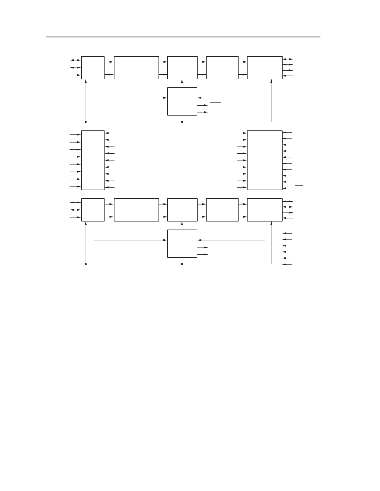
1.4 SRC4194EVM Functional Block Diagram
The SRC4194EVM functional block diagram is shown in Figure 1−2. Besides
the SRC4194, there are multiple audio input and output port interfaces, reference clock generation circuitry, switches for Hardware mode configuration and
logic functions, and a buffered host port interface for communications with the
SRC4194 SPI port when configured for Software mode operation. Chapter 3
provides operational and configuration details for the various hardware functions included on the EVM board.
Figure 1−2. SRC4194EVM Functional Block Diagram
AES
OUT B
OUTPUT
PORT B
AES3 Tx
DIT4192
SW8
H
D
R
PORT
BUFFERS
DIT
CLOCK B
SW10
CLOCK GEN
PLL1705
RCKIB
SRC B
EXT CLOCK
SW4 SW5
AES
IN B
AES
IN A
AES
OUT A
INPUT
PORT B
INPUT
PORT A
OUTPUT
PORT A
AES3 Rx
CS8414
SW8
H
D
R
H
D
R
H
D
R
PORT
BUFFERS
PORT
BUFFERS
SW6
AES3 Rx
CS8414
PORT
BUFFERS
SW6
AES3 Tx
DIT4192
DIT
CLOCK A
4−CHANNEL ASYNCHRONOUS
SAMPLE RATE CONVERTER
SRC4194
RCKIA
CLOCK GEN
PLL1705
SW10
Power Supplies are not shown in this diagram. Refer
to Figure 3−1 for power supply configuration details
SW1
SRC A
EXT CLOCK
SW2
HOST PORT
BUFFER
HDR
HOST
PORT
1-6
Page 17

Chapter 2
This chapter provides information regarding SRC4194EVM handling and
unpacking, as well as absolute operating conditions.
Topic Page
2.1 Electrostatic Discharge Warning 2-2. . . . . . . . . . . . . . . . . . . . . . . . . . . . . . .
2.2 Unpacking the EVM 2-3. . . . . . . . . . . . . . . . . . . . . . . . . . . . . . . . . . . . . . . . . . .
2.3 Absolute Maximum Operating Conditions 2-4. . . . . . . . . . . . . . . . . . . . . . .
Getting Started
2-1
Page 18

Electrostatic Discharge Warning
2.1 Electrostatic Discharge Warning
Failure to observe proper ESD handling precautions may result in
damage to EVM components.
Many of the components on the SRC4194EVM are susceptible to damage by
electrostatic discharge (ESD). Customers are advised to observe proper ESD
handling procedures when unpacking and handling the EVM, including the
use of a grounded wrist strap at an approved ESD workstation. Failure to observe ESD handling procedures may result in damage to EVM components.
2-2
Page 19

2.2 Unpacking the EVM
Upon opening the SRC4194EVM package, please check to make sure that the
following items are included:
- One SRC4194EVM
- One printed copy of the SRC4194 data sheet
- One printed copy of the SRC4194EVM User’s Guide
If any of these items are missing, please contact the Texas Instruments Product Information Center nearest you to inquire about replacements.
Unpacking the EVM
Getting Started
2-3
Page 20

Absolute Maximum Operating Conditions
2.3 Absolute Maximum Operating Conditions
Exceeding the Absolute Operating Conditions may result in
damage to the evaluation module and/or the equipment connected
to it.
The user should be aware of the absolute operating conditions for the
SRC4194EVM. Exceeding these conditions may result in damage to the EVM
and possibly the equipment connected to it. Table 2−1 summarizes the critical
data points.
Table 2−1.Absolute Operating Conditions
Power Supplies
+5V +4.5 +6.0 V
EXT +1.8V +1.65 +2.0 V
EXT +3.3V +3.0 +3.6 V
EXT VIO
Input Port A and B, Output Port A and B, Host Port, SRC A and B EXT Clock, and DIT
Clock A and B
V
V
AES IN A and B Ports
V
V
(1)
(1)
(1)
IH
IL
IH
IL
VIO may be set to +1.8V or +3.3V using onboard regulators, or +1.65V to +3.6V using an
external power supply connected to the EXT VIO terminal located on connector J14.
MIN MAX UNIT
+1.65 +3.6 V
VIO + 0.3 V
−0.3 V
+7.0 V
−0.5 V
2-4
Page 21

Chapter 3
This chapter provides hardware description and configuration information for
the SRC4194EVM.
Topic Page
3.1 Power Supply Configuration 3-2. . . . . . . . . . . . . . . . . . . . . . . . . . . . . . . . . . .
3.2 SRC4194 Configuration Modes 3-4. . . . . . . . . . . . . . . . . . . . . . . . . . . . . . . . .
SRC4194 Hardware (or Standalone) Mode Configuration 3-4. . . . . . . . . . . .
SCR4194 Software Mode Configuration Via The Host Port 3-6. . . . . . . . . . .
3.3 Audio Input Ports 3-7. . . . . . . . . . . . . . . . . . . . . . . . . . . . . . . . . . . . . . . . . . . . .
3.4 Audio Output Ports 3-8. . . . . . . . . . . . . . . . . . . . . . . . . . . . . . . . . . . . . . . . . . .
3.5 Reference Clock Generation 3-10. . . . . . . . . . . . . . . . . . . . . . . . . . . . . . . . . .
3.6 TDM Test Mode 3-11. . . . . . . . . . . . . . . . . . . . . . . . . . . . . . . . . . . . . . . . . . . . . .
Hardware Description and Configuration
3-1
Page 22

Power Supply Configuration
3.1 Power Supply Configuration
Changes to settings for jumpers J15 through J17, as well as
changes to the state of the REGEN element of switch SW2, should
be performed with all power supplies connected to terminal block
J14 powered off, thereby avoiding potential damage to the EVM a n d
external components.
The SRC4194EVM provides several options for power-supply configuration
using onboard regulators and/or external supplies. Onboard jumpers and a
switch are used to select the available options. Figure 3−1 illustrates the EVM
power-supply configuration using jumpers J15 through J17 and terminal block
J14. Table 3−1 summarizes the common jumper configurations based upon
a setup using a +5V supply and an optional EXT VIO supply.
Figure 3−1.SRC4194EVM Power Supply Configuration and Jumpers
+5V GND GND +1.8V +3.3V
EXT
EXT
+1.8V
+3.3V
U32
+3.3V
+5V
REG
U33
+1.8V
REG
NOTE: (1) NC = not connected.
EXT
VIO
EXT
VIO
REG +3.3V
REG +1.8V
J14
VIO
VDD33
VDD18
REG +1.8V
J15
65
43
21
J16
J17
NC
NC
(1)
(1)
REG +3.3V
EXT VIO
REG +3.3V
EXT +3.3V
REG +1.8V
EXT +1.8V
Referring to Figure 3−1, the SRC4194EVM includes two onboard linear voltage regulators, U32 and U33, which are used to derive +1.8V and +3.3V from
a single +5V external power supply. The outputs of the two regulators may be
connected to the onboard VDD18, VDD33, or VIO power busses using jumpers J15 through J17. The jumpers also allow for connection to external power
supplies using terminal block J14.
Table 3−1 summarizes five common supply configurations for the
SRC4194EVM. Jumper settings for J15 through J17 are indicated, as well as
the state of the REGEN element of switch SW2. The user is reminded to power
down all supplies connected to terminal block J14 of the EVM before changing
the jumper and switch configurations.
3-2
Page 23

Power Supply Configuration
1
2
3
4
5
Table 3−1.Common Configurations using a +5V Supply and an Optional EXT VIO Supply
Case Description J15 J16
Core Voltage = +1.8V
using onboard regulator (U33)
VIO = +1.8V
using onboard regulator (U33)
Core Voltage = +1.8V
using onboard regulator (U33)
VIO = +3.3V
using onboard regulator (U32)
Core Voltage = +3.3V
using onboard regulator (U32)
VIO = 3.3V
using onboard regulator (U32)
Core Voltage = +1.8V
using onboard regulator (U33)
VIO = +1.65V to 3.6V
using EXT VIO supply
Core Voltage = +3.3V
using onboard regulator (U32)
VIO = +1.65V to 3.6V
using EXT VIO supply
— NC REG + 1.8V LO
REG + 1.8V
— NC REG + 1.8V LO
REG + 3.3V
— REG + 3.3V NC HI
REG + 3.3V
— NC REG + 1.8V LO
EXT VIO
— REG + 3.3V NC HI
EXT VIO
(1)
J17
(1)
REGEN
(SW2)
1) NC = not connected.
Hardware Description and Configuration
3-3
Page 24

SRC4194 Configuration Modes
3.2 SRC4194 Configuration Modes
The SRC4194 can be set to one of two configuration modes: Hardware (or
Standalone) or Software (via a four-wire SPI port). The H/S
SW2 is used to set the mode. Table 3−2 summarizes the H/S
tings.
Table 3−2.Setting the Configuration Mode
H/S Switch Setting SRC4194 Configuration Mode
LO Software Mode
HI Hardware (or Standalone) Mode
3.2.1 SRC4194 Hardware (or Standalone) Mode Configuration
In Hardware mode, switches SW1, SW2, SW4, and SW5 are used to set the
dedicated control pins to either a low or high logic level. The switches correspond one-to-one with the pin names of the SRC4194 device. Table 3−3 summarizes the switch functions and available settings for each element of switch
SW1, SW2, SW4, and SW5.
element of switch
mode switch set-
In addition to the switches already mentioned, a momentary pushbutton switch
(SW3) is used for the SRC4194 reset function. The RST
input (pin 21) of the
SRC4194 is normally pulled high via an external 10kΩ resistor connected to
the VIO supply bus. When the pushbutton is pressed, the switch shorts the
pin to ground. Releasing the switch then causes the RST pin to be pulled
RST
high again. By momentarily pressing and then releasing SW3, the user can
generate a reset pulse for the SRC4194.
3-4
Page 25

S
2
Input Port Data Format
S
2
Output Port Data Format
Output Port Word Length
Bypass Mode
Interpolation Filter Group Delay
SRC4194 Configuration Modes
Decimation Mode
De-Emphasis Filter Function
Output Soft Mute
Input & Output Serial Port Mode
HI LO LO Output Port is Master w/ RCKI =128fs
HI HI LO Output Port is Master w/ RCKI =256fs
HI LO HI Input Port is Master w/ RCKI =128fs
LO LO LO Input and Output Ports are Slave
LO HI LO Output Port is Master w/ RCKI =512fs
HI HI HI Input Port is Master w/ RCKI =256fs
LO LO HI Input and Output Ports are Slave
LO HI HI Input Port is Master w/ RCKI =512fs
HI Enabled
LO Disabled
HI LO I
LO LO Left Justified
LO HI TDM
HI LO 20 bits
LO LO 24 bits
HI HI Right Justified
HI HI 16 bits
LO HI 18 bits
HI LO Buffer 32 samples before resampling
HI HI Buffer 8 samples before resampling
LO LO Buffer 64 samples before resampling
LO HI Buffer 16 samples before resampling
HI Enabled
LO Disabled
HI LO Enabled for fs = 48kHz
HI HI Enabled for fs = 32kHz
LO LO Disabled
LO HI Enabled for fs = 44.1kHz
HI Direct Downsampling Enabled
LO Decimation Filter Enabled
HI LO LO 24-bit I
HI HI LO Unused
HI LO HI 18-bit Right Justified
LO LO LO 24-bit Left Justified
IFMTx0 IFMTx1 IFMTx2 OFMTx0 OFMTx1 OWLx0 OWLx1 BYPx LRGPx0 LGRPx1 DDNx DEMx0 DEMx1 MODEx0 MODEx1 MODEx2 MUTEx Function/Description
Table 3−3.Hardware Mode Setup Matrix Using Switches SW1, SW2, SW4 and SW5 (x = A or B)
LO HI LO Unused
HI HI HI 24-bit Right Justified
LO LO HI 16-bit Right Justified
LO HI HI 20-bit Right Justified
Hardware Description and Configuration
3-5
Page 26

3.2.2 SRC4194 Software Mode Configuration Via The Host Port
In Software mode, the SRC4194 relies upon an external host device to program the internal control registers via the four-wire SPI port. The SPI port is
accessed using the Host Port header, connector J1. The header is buffered
by U2, an octal buffer IC with tri-state outputs. The buffer outputs are enabled
only when the H/S
HI, the buffer outputs are set to a high-impedance state.
The Host Port header provides a convenient interface point for connection to
an external host device, such as a microprocessor, a digital signal controller/
processor, or a digital input/output card installed in a PC.
Refer to the SRC4194 datasheet for a description of the SPI port protocol and
control register definitions.
element of switch SW2 is set to the LO state. When H/S is
3-6
Page 27

3.3 Audio Input Ports
The SRC4192EVM includes four audio input ports, two each for the SRC A and
SRC B sections of the SRC4194. Each section is provided with an
AES3/SPDIF-compatible input, along with a buffered I/O header. Figure 3−2
illustrates the input port external connections and associated switch settings.
Figure 3−2.Input Port External Connections and Configuration
Audio Input Ports
Switch SW6 or SW8
x_DIR
LO = OutputEnabled
HI = Output Disabled
U14 or U24
CS8414−CS
SCK
FSYNC
SDAT A
NOTE: x = A or B
RCKIx
SDINx
LRCKx
BCKx
2
1
Switch SW6 or SW8
x_IM/S
LO = SRC is Slave
HI = SRC is Master
U1
SRC4194IPAG
BCKx
LRCKx
SDINx
RCKIx
From
RCKIx
Source
INPUT PORT A (J5)
or
INPUT PORT B (J10)
The SRC A section input port selection and Master/Slave mode operation are
configured using the A_DIR and A_IM/S elements of switch SW6. The SRC
B section input port selection and Master/Slave mode operation are configured using the B_DIR
and B_IM/S elements of switch SW8.
The AES IN A (J6) and AES IN B (J11) connectors accept 75Ω coaxial cable
connections terminated with RCA plugs. The onboard AES3 receivers (U14
and U24) recover audio clocks and data from the AES3 encoded input stream.
The receivers are configured to output 24-bit I
serial bit (or data) clock rate of 64f
fs is the frame or sampling rate of the incoming AES3-formatted data stream.
Sampling rates up to 108kHz are supported. The AES IN A and B input ports
provide a convenient, standard interface to consumer and professional audio
equipment, as well as common audio test systems.
The buffered input serial ports INPUT PORT A (J5) and INPUT PORT B (J10)
support Left-Justified, Right-Justified, and I
lengths up to 24 bits and sampling rates up to 212kHz. The input ports may
be operated in either Slave or Master mode, but must match the input port setup for the SRC4194 device, as defined in Table 3−3. The buffered serial input
ports provide a convenient method for interfacing to audio devices that support
an audio serial data interface, including external digital audio receivers, audio
data converters, and digital signal processing components.
2
S-formatted audio data with a
and a left/right word clock rate of fs, where
s
2
S-formatted audio data with word
3-7
Page 28
Audio Output Ports
3.4 Audio Output Ports
The SRC4192EVM includes four audio output ports, two each for the SRC A
and SRC B sections of the SRC4194. Each section is provided with an
AES3/SPDIF-compatible output, along with a buffered I/O header. Figure 3−3
illustrates the output port external connections and associated switch settings.
The SRC A section output port selection and Master/Slave mode operation are
configured using switch SW6. The SRC B section output port selection and
Master/Slave mode operation are configured using switch SW8.
The AES OUT A (J3) and AES OUT B (J8) connectors accept 75Ω coaxial
cable connections terminated with RCA plugs. The onboard AES3 transmitters (U7 and U17) provide the AES3 encoded data streams for each output.
Both transmitters are configured to accept 24-bit I
sampling rates up to 192kHz. The AES OUT A and B output ports provide a
convenient, standard interface to consumer and professional audio equipment, as well as common audio test systems.
Figure 3−3.Output Port External Connections and Configuration
Switch SW6 or SW8
U1
SRC4194IPAG
x_OM/S
LO =SRC is Slave
HI = SRC is Master
NOTE: x = Aor B
2
S-formatted audio data at
U7 or U17
DIT4192IPW
From
RCKIx
Source
BCKx
LRCKx
SDOUTx
TDMIx
RCKIx
RCKIx
TDMIx
SDOUTx
LRCKx
BCKx
2
1
OUTPUTPORTA(J2)
OUTPUTPORTB (J7)
or
Switch SW6 or SW8
x_OM/S
LO = DIT CLOCK x
HI = RCKI x
DIT CLOCKA (J4)
or
DIT CLOCK B (J9)
SCLK
SYNC
SDATA
MCLK M/S
Switch SW6 or SW8
x_DIT
LO = DIT is Slave Only
HI = See Text BoxBelow
Switch SW6 or SW8
x_OM/S
LO = DIT is Master
HI = DIT is Slave
3-8
Page 29

Audio Output Ports
The DIT4192 transmitters (U7 and U17) have additional configuration
switches, summarized in Table 3−4 and Table 3−5. For the clock divider, the
corresponding control pins need to be set dependent upon the incoming master clock (MCLK) and output sampling rates, f
. The master clock (MCLK)
Sout
rate is set by either reference clock RCKIA or RCKIB, or by the corresponding
DIT CLOCK input at connector J4 or J9 (dependent upon the clock configuration; see Figure 3−3 and Figure 3−4).
Stereo mode operation is the default for most test cases. The Mono mode configuration is utilized primarily to support testing at 176.4kHz and 192kHz output
sampling rates using an Audio Precision System Two Cascade or Cascade
Plus test system with Dual Channel mode support.
The buffered output serial ports OUTPUT PORT A (J2) and OUTPUT PORT
2
B (J7) support Left-Justified, Right-Justified, I
S, and time division multiplexed
(TDM) formatted audio data with word lengths up to 24 bits and sampling rates
up to 212kHz. The output ports may be operated in either Slave or Master
mode, but must match the output port setup for the SRC4194 device as defined in Table 3−3. The buffered serial output ports provide a convenient method for interfacing to audio devices which support an audio serial data interface,
including external digital audio transmitters, audio data converters, and signal
processing components.
Table 3−4.Transmitter Clock Divider Configuration
If MCLK Rate Equal To: Set Transmitter Clock Divider Switches To:
128 × f
256 × f
384 × f
512 × f
Where f
sOUT
sOUT
sOUT
sOUT
= the output sampling rate Where x = A (switch SW6) or B (switch SW8)
sOUT
x_CLK0 = LO, x_CLK1 = LO
x_CLK0 = HI, x_CLK1 = LO
x_CLK0 = LO, x_CLK1 = HI
x_CLK0 = HI, x_CLK1 = HI
Table 3−5.Transmitter Stereo/Mono Mode Configuration
Transmitter Output Mode Set Mode Switches To:
Stereo x_MONO = LO, x_MDAT = LO
Mono with Left Channel Data Source x_MONO = HI, x_MDAT = LO
Mono with Right Channel Data Source x_MONO = HI, x_MDAT = HI
Where x = A (switch SW6) or B (switch SW8)
3-9
Page 30

Reference Clock Generation
3.5 Reference Clock Generation
The SRC4194EVM supports a flexible configuration for the SRC4194 reference clock generation. Figure 3−4 illustrates the PLL and clock connections
used for the reference clocks.
Both SRC A and SRC B have their own reference clocks, referred to as RCKIA
and RCKIB, respectively. The reference clocks may be derived by onboard
PLL clock generators (U25 and U28), or by external clock sources applied at
connectors J12 and J13. Table 3−6 summarizes the output rates available
from the onboard PLL circuits.
The reference clocks are also used by the transmitter sections of the EVM, and
are made available at the audio input and output ports for use by external hardware.
Figure 3−4.Reference Clock Generation, Connections, and Configuration
SRC A EXT
CLOCK (J12)
To RCKIA
SRC B EXT
CLOCK (J13)
To RCKIB
Switch SW 10
A_PLL
LO = UsePLL (U25)
HI = Use Ext Clock (J12)
U25
PLL1705DBQ
SCKO2
FS1
FS2
Switch SW10
A_FS1
A_FS2
A_SR
SR
Switch SW10
B_PLL
LO = Use PLL (U28)
HI = Use Ext Clock (J13)
U28
PLL1705DBQ
SCKO2
FS1
FS2
Switch SW10
B_FS1
B_FS2
B_SR
Switch SW10
B_CLK
LO = Use PLL or EXT CLK
HI = Use RCKIA
SR
Table 3−6.PLL Configuration for U25 and U28
x_SR (switch SW10) x_FS2 (switch SW10) x_FS1 (switch SW10) PLL Output Rate
LO LO LO 12.288 MHz
LO LO HI 11.2896 MHz
LO HI LO 8.192 MHz
LO HI HI Reserved
HI LO LO 24.576 MHz
HI LO HI 22.5792 MHz
HI HI LO 16.384 MHz
HI HI HI Reserved
Where x = A or B Where x = A or B Where x = A or B
3-10
Page 31

3.6 TDM Test Mode
Jumper J18 is provided to allow a simple onboard connection between
SDOUT A ( pin 64) and TDMIB (pin 52). This provides a test mode for evaluating
the TDM output data format. When J18 is shorted, the TDMIB pin at header
J7 should be floating, with no external connection.
TDM Test Mode
3-11
Page 32

3-12
Page 33

Chapter 4
! "# ! $
This chapter provides the electrical schematic and physical layout information
for the SRC4194EVM. The bill of materials is included for component and
manufacturer reference.
Topic Page
4.1 Schematic 4-2. . . . . . . . . . . . . . . . . . . . . . . . . . . . . . . . . . . . . . . . . . . . . . . . . . . .
4.2 PCB Layout 4-5. . . . . . . . . . . . . . . . . . . . . . . . . . . . . . . . . . . . . . . . . . . . . . . . . .
4.3 Bill of Materials 4-11. . . . . . . . . . . . . . . . . . . . . . . . . . . . . . . . . . . . . . . . . . . . . .
Schematic, PCB Layout, and Bill of Materials
4-1
Page 34

Schematic
4.1 Schematic
The electrical schematic for the SRC4194EVM is shown in Figure 4−1 and
Figure 4−2. Descriptions of the components shown on the schematics are
listed in Table 4−1.
4-2
Page 35

Figure 4−1.SRC4194EVM Schematic Diagram, Page 1 of 2
C41
0.1uF
10uF
C31
VIO
20
U5
1
0.1uF
B118B217B316B415B514B613B712B8
VCC
A12A23A34A45A56A67A78A8
DIR
+5V
23
28
25
24
21
26
U27V
BLS
BLSM
EMPH
MODE
AUDIO22MONO
CSS1COPY/C2L3CLK14CLK05MCLK6VIO7DGND8FMT09FMT110SCLK11SYNC12SDATA13M/S
U7
VIO
100
10uF
C32
0.1uF
C11
RN16
19
11
OE
GND
9
10
U6A
C29
0.1uF
VCC20GND
VIO
G1A1
C13
18
16
20
15
17
TX−
RST
VDD19TX+
MDAT
DGND
14
C33
VIO
SN74ALVC245PW
SN74LVC1G04DBV
18
16
14
12
Y1
Y2
Y3
Y4
10
A2
A3
A4
2
4
6
8
J3
C42
0.1uF
AES OUT A
R4
120
R6
150
C2
0.01uF
J4
6
8
11
1Y
2Y
3Y
4Y
1OE
2OE
3A93OE
4A124OE
11A2
42A5
10
RN15
SN74ALVC244PW
DIT CLOCKA
R8
75
7
GND
SN74ALVC125PW
13
100
J18
C36
VIO
20
J2
OUTPUT PORT A
9 10
7 8
6
5
U15
4
3
1
2
1
1 2
TDM
DIT4192IPW
SW7
R2
10K
A_DITRST
VIO
453U8
SN74LVC1G08DBV
VIO
0.1uF
C34
C35
0.1uF
VIO
1
2
3
14
VCC
U9
U10
53
2 4
0.1uF
9
7
5
3
U6B
Y1
Y2
Y3
Y4
SN74ALVC244PW
G19A1
A2
A3
A4
11
13
15
17
C43
+5V
VIO
28U27V26
25
24
23
BLS
BLSM
MODE
CSS1COPY/C2L3CLK14CLK05MCLK6VIO7DGND8FMT09FMT110SCLK11SYNC12SDATA13M/S
U17
VIO
C37
C12
0.1uF
0.1uF
B118B217B316B415B514B613B712B8
VCC
A12A23A34A45A56A67A78A8
DIR
C30
VIO
EMPH
11
9
0.1uF
0.1uF
10uF
C14
18
20
21
17
VDD19TX+
MDAT
AUDIO22MONO
RN19
10uF
19
OE
GND
SN74ALV C245PW
10
18
16
Y1
Y2
U16A
VCC20GND
G1A1
A2
2
4
Schematic
J8
R7
150
AESOUT B
R5
120
C3
C44
0.1uF
0.01uF
SW9
16
15
TX−
RST
DGND
14
100
SN74LVC1G04DBV
14
12
Y3
Y4
A3
A4
6
8
B_DITRST
J9
DIT CLOCKB
R9
R3
DIT4192IPW
VIO
453U18
VIO
1
C38
0.1uF
53
VIO
C39
0.1uF
10
SN74ALVC244PW
75
10K
C40
0.1uF
VIO
SN74LVC1G08DBV
2
U19
U20
2 4
9
7
5
U16B
Y1
Y2
G19A1
A2
11
13
15
14
3
Y3
A3
17
3
1Y
VCC
3A93OE
Y4
A4
SN74ALVC244PW
6
8
11
2Y
3Y
4Y
1OE
2OE
4A124OE
11A2
42A5
7
GND
SN74ALVC125PW
10
13
RN18
100
9 10
7 8
6
5
4
3
2
1
J7
OUTPUT PORT B
B_/DIR
B_IM/S
A_/DIR
A_IM/S
VIO
RN9
RN10
10K
VIO
SW6
1 16
2 15
3 14
4 13
5 12
6 11
7 10
8 9
BCKIB
LRCKIB
SDINB
RN1
100
BCKIA
LRCKIA
SDINA
VIO
C8
SW4
1 20
2 19
3 18
4 17
5 16
RN7
10K
RN6
10K
VIO
48
45
U1
IFMTB246IFMTB147IFMTB0
SDOUTB
49
BCKOB
50
LRCKOB
51
TDMIB
52
BCKIB
53
LRCKIB
54
SDINB
55
VIO
56
C23
0.1uF
10uF
VIO
DGND
57
SDINA
58
LRCKIA
59
BCKIA
60
TDMIA
61
LRCKOA
62
BCKOA
63
SDOUTA
64
1
RN3
10K
RN2
10K
SW5
6 15
7 14
8 13
9 12
1 20
2 19
3 18
4 17
5 16
10 11
38
41
43
40
BYPB
OWLB142OWLB0
LGRPB139LGRPB0
OFMTB144OFMTB0
6 15
34
33
35
37
36
DDNB
DEMB0
MODEB0 (CS)
MODEB2 (CDIN)
MODEB1 (CCLK)
DEMB1(CDOUT)
RATIOB
RDYB
MUTEB
RCKIB
VDD18
VDD18
REGEN
VDD33
VDD33
DGND
H/S
RST
RCKIA
MUTEA
RDYA
RATIOA
MODEA216MODEA115MODEA014DEMA113DEMA012DDNA11LGRPA110LGRPA09BYPA8OWLA17OWLA06OFMTA15OFMTA04IFMTA23IFMTA12IFMTA0
D1
10K
7 14
8 13
9 12
10 11
RN8
10K
1
G
U3A
VCC20GND
VIO
C27
0.1uF
VIO
/RDYB
D4
SRC4194IPAG
D3
32
RATIOB
31
30
29
28
27
26
25
24
23
22
21
20
19
18
17
D2
VIO
RATIOA
RCKIB
C26
0.1uF
C10
10uF
C24
0.1uF
VDD33 VDD18
C9
10uF
/RDYA
RCKIA
RN5
10K
VIO
RN4
10K
18
Y1
U2A
VCC20GND
VIO
G1A1
2
C25
0.1uF
RN14
246
R20
10K
135
VIO
J1
R1
10K
VIO
VIO
10K
RN11
U4
SW8
1 16
2 15
3 14
4 13
5 12
6 11
7 10
17
A3
Y3
3
G19A1
8 9
A4
Y4
SN74ALVC244PW
9
7
5
3
SN74ALVC244PW
Y1
Y2
Y3
Y4
A2
A3
A4
11
13
15
17
53
VIO
2
4
6
A1
A2
A3
Y1
Y2
Y3
18
16
14
16
14
12
Y2
Y3
Y4
A2
A3
A4
4
6
8
7 8
SW3
2 4
8
C28
0.1uF
A4
SN74ALVC244PW
10
Y4
12
SN74ALVC244PW
10
9 10
C1
0.01uF
RST
SN74LVC1G04DBV
11
13
15
19
U2B
G
A1
A2
Y1
Y2
9
7
5
100
HOST PORT
U3B
VIO
SW1
1 20
2 19
3 18
4 17
5 16
SW2
6 15
7 14
8 13
9 12
1 20
2 19
3 18
4 17
5 16
6 15
7 14
8 13
10 11
9 12
10 11
Schematic, PCB Layout, and Bill of Materials
4-3
Page 36

Schematic
Figure 4−2.SRC4194EVM Schematic Diagram, Page 2 of 2
VIO
VDD33
VDD18
1 2
3 4
5 6
1 2
3 4
5 6
1 2
3 4
J15
18
16
14
12
U23A
C70
0.1uF
VIO
C61
0.1uF
VIO
A_IM/S
BCKIA
LRCKIA
9
1
U11
DIR
VCC
20
VIO
C55
0.1uF
A_/DIR
10
A12A23A34A45A56A67A78A8
B118B217B316B415B514B613B712B8
11
9
7
5
3
Y1
Y2
Y3
U12B
G19A1
A2
A3
11
13
15
17
9
7
5
3
Y1
Y2
Y3
Y4
U13B
G19A1
A2
A3
A4
11
13
15
17
+5V
R16
475
LOCK A
D5
27
25
26
28
ERF
VERF
CE/F2
SDATA
C1CD/F12CC/F03CB/E24CA/E15C0/E06VDD7DGND8RXP9RXN10FSYNC11SCK12CS12/FCK13U
U14
+5V +5V
SN74LVC244APW
Y1
Y2
Y3
Y4
VCC20GND
10
G1A1
A2
A3
A4
2
4
6
8
18
16
14
12
U13A
SN74LVC244 APW
Y1
Y2
Y3
Y4
VCC20GND
10
G1A1
A2
A3
A4
2
4
6
8
GND
OE
SN74ALVC245PW
19
18
16
14
12
Y1
Y2
Y3
SDINA
Y4
A4
SN74LVC2 44APW
22M023M124
VCC
U12A
VCC20GND
VIO
G1A1
A2
C56
SN74ALVC244PW
RN17
100
C72
C18
10uF
C49
0.1uF
20
21
19
FILT
MCK
AGND
C45
0.1uF
C15
10uF
C4
0.01uFC50.01uF
J6
AESIN A
A3
0.1uF
2
4
6
8
9 10
7 8
6
5
4
3
2
1
J5
INPUTPORTA
0.068uF
R17
475
15
16
18
M317M2
SEL
CBL
CS8414−CS
14
R10
75
J16
EXTVIOREG +3.3VREG +1.8V
EXT VDD33REG +3.3V
+5V
1
2
3
4
5
6
J14
POWER SUPPLIES
EXTVIO
B_IM/S
BCKIB
1
U21
DIR
VCC
20
VIO
C57
0.1uF
Y4
SN74ALVC244PW
10
A4
B_/DIR
5 6
J17
EXT VDD18REG +1.8V
C71
0.1uF
C83
100uF
C63
0.1uF
EXT VDD18
C84
0.1uF
C62
EXT VDD33
C82
100uF
LRCKIB
A12A23A34A45A56A67A78A8
B118B217B316B415B514B613B712B8
U22B
G19A1
9
Y1
U23B
G19A1
11
+5V
R18
475
LOCK B
D6
27
28
VERF
CE/F2
C1CD/F12CC/F03CB/E24CA/E15C0/E06VDD7DGND8RXP9RXN10FSYNC11SCK12CS12/FCK13U
U24
U33
100uF
C64
0.1uF
C85
100uF
U32
9
10
GND
OE
SN74ALVC245PW
11
19
SDINB
9
7
5
3
Y1
Y2
Y3
Y4
SN74ALVC244PW
A2
A3
A4
11
13
15
17
7
5
3
RN20
Y2
Y3
Y4
A2
A3
A4
SN74LVC2 44APW
13
15
17
C19
10uF
C50
0.1uF
21
25
26
22M023M124
ERF
VCC
AGND
SDATA
C46
0.1uF
C16
10uF
+5V +5V
J11
REG1117A−1.8
REG +3.3V +5V REG +1.8V+5V
REG1117−3.3
100
C6
AESIN B
C81
2
VOUT
VIN
3
C80
C79
2
VOUT
VIN
3
C78
VIO
C58
20
19
FILT
10uF
GND
1
10uF
10uF
GND
1
10uF
U22A
0.1uF
J10
C73
0.068uF
R19
475
16
18
M317M2
MCK
0.01uFC70.01uF
R11
75
SEL
6
4
2
G1A1
INPUTPORTB
15
CBL
14
18
16
Y1
VCC20GND
2
4
9 10
7 8
5
3
1
CS8414−CS
14
12
Y2
Y3
Y4
SN74ALVC244PW
10
A2
A3
A4
6
8
C66
0.1uF
C21
RN13
RN12
REG+3.3V
REG +3.3V
REG +3.3V
VIO
C65
10K
10K
C51
C67
0.1uF
0.1uF
U29
SW10
0.1uF
C20
C52
0.1uF
C47
VIO
U26
VIO
10uF
19
20
VDD3
VDD11SCKO22SCKO33DGND14FS15FS26SR7VCC8AGND9XT1
U28
3
6
14
1Y
VCC
3A93OE
J13
SRC BEXT CLOCK
1 20
2 19
3 18
4 17
10uF
19
20
VDD3
VDD11SCKO22SCKO33DGND14FS15FS26SR7VCC8AGND9XT1
U25
0.1uF
14
3
6
1Y
VCC
3A93OE
J12
SRC A EXTCLOCK
REG +3.3V
REG +3.3V
17
SCKO118SCKO0
8
11
2Y
3Y
4Y
1OE
2OE
4A124OE
11A2
42A5
10
R14
75
5 16
6 15
7 14
17
SCKO118SCKO0
R13
8
11
2Y
3Y
4Y
1OE
2OE
4A124OE
11A2
42A5
10
R12
75
C68
0.1uF
C77
27pF
11
12
13
XT2
CSEL
VDD2
MCKO114MCKO215DGND216DGND3
X2
27.000MHz
PLL1705DBQ
C76
27pF
10
C69
0.1uF
R15
75
C22
10uF
REG +3.3V
7
GND
RCKIB
SN74ALVC125PW
13
U30
53
VIO
C59
0.1uF
8 13
9 12
10 11
12
13
CSEL
VDD2
MCKO114MCKO215DGND216DGND3
75
7
GND
SN74ALVC125PW
13
U31
SN74LVC1G04DBV
53
VIO
2 4
C60
0.1uF
RCKIA
2 4
SN74LVC1G04DBV
C53
0.1uF
C75
27pF
11
XT2
X1
27.000 MHz
PLL1705DBQ
C74
27pF
10
C54
0.1uF
C17
10uF
REG +3.3V
U27
53
VIO
2 4
C48
0.1uF
SN74LVC1G04DBV
4-4
Page 37

4.2 PCB Layout
The SRC4194EVM is a four-layer printed circuit board (PCB) with the following
layer structure:
- Layer 1: Top (Component Side)
- Layer 2: Ground Plane
- Layer 3: Power
- Layer 4: Bottom (Solder Side)
Figure 4−3 through Figure 4−8 show the top side silk screen, along with the
top, ground plane, power, and bottom layers of the printed circuit assembly.
Figure 4−3.Top Side Silk Screen
PCB Layout
Schematic, PCB Layout, and Bill of Materials
4-5
Page 38

PCB Layout
Figure 4−4.Bottom Side Silk Screen
4-6
Page 39

Figure 4−5.Top Layer (Component Side)
PCB Layout
Schematic, PCB Layout, and Bill of Materials
4-7
Page 40

PCB Layout
Figure 4−6.Ground Plane Layer
4-8
Page 41

Figure 4−7.Power Layer
PCB Layout
Schematic, PCB Layout, and Bill of Materials
4-9
Page 42

PCB Layout
Figure 4−8.Bottom layer (Solder Side)
4-10
Page 43

DESCRIPTION
50WV, Size = 0603
16WV, Size = 0603
50WV, Size = 0603
Size = A
16WV, Size = 0603
Size = D
Bill of Materials
Size = 0805
Size = 0805
Chip Capacitor, NPO/C0G Ceramic, 27pF, ±5%,
PART NUMBER
MANUFACTURER
MFG
BOARD
QTY PER
Chip Capacitor, X7R Ceramic, 0.01µF, ±5%,
Chip Capacitor, X7R Ceramic, 0.068µF ±5%,
Chip Capacitor, X7R Ceramic, 0.1µF ±10%,
Resistor, 75Ω, ±1%, 1/10W, Thick Film Chip,
Chip Capacitor, Tantalum, 10µF ±10%, 10WV,
Chip Capacitor, Tantalum, 100µF ±10%, 10WV,
Resistor, 120Ω, ±1%, 1/10W, Thick Film Chip,
The bill of materials, listing the components used in the assembly of the SRC4194EVM, is shown in Table 4−1.
REFERENCE
DESIGNATOR
4.3 Bill of Materials
Table 4−1.SRC4194EVM Bill of Materials
ITEM VALUE
1 27pF C74−C77 4 Kemet C0603C270J5GACTU
2 0.01µF C1−C7 7 Kemet C0603C103J5RACTU
3 0.068µF C72, C73 2 Kemet C0603C683J4RACTU
4 0.1µF C23−C71 49 Kemet C0603C104K4RACTU
5 10µF C8−C22, C78−C81 19 Kemet T491A106K010AS
6 100µF C82−C85 4 Kemet T491D107K010AS
7 J1, J2, J5, J7, J10 5 Samtec TSW−105−07−G−D Terminal Strip, 10-pin (5x2)
8 J3, J6, J8, J11 4 CUI Stack RCJ−041 RCA Jack, PC Mount, Black
9 J4, J9, J12, J13 4 Kings Electronics KC−79−274−M06 BNC Connector, Female, PC Mount
Schematic, PCB Layout, and Bill of Materials
11 J15−J17 3 Samtec TSW−103−07−G−D Terminal Strip, 6-pin (3x2)
10 J14 1 Weidmuller 9967720000 Terminal Block, 3.5mm PCB, 6 poles
12 J18 1 Samtec TSW−102−07−G−S Terminal Strip, 2-pin (2x1)
13 D1−D6 6 Lumex SML−LX1206GC−TR Green LED, SMT, Size = 1206
14 75Ω R8−R15 8 Panasonic or equivalent ERJ−6ENF75R0V
15 120Ω R4, R5 2 Panasonic or equivalent ERJ−6ENF1200V
4-11
Page 44

Bill of Materials
Size = 0805
Size = 0805
Size = 0805
Terminal
Converter
Resistor, 150Ω, ±1%, 1/10W, Thick Film Chip,
PART NUMBER
MANUFACTURER
MFG
Thick Film Chip Resistor Array, 100Ω,
Resistor, 10kΩ, ±1%, 1/10W, Thick Film Chip,
Resistor, 475Ω, ±1%, 1/10W, Thick Film Chip,
8-terminal, 4 resistors
16-terminal, 8 resistors
Thick Film Chip Resistor Array, 100Ω,
16-terminal, 8 resistors
Thick Film Chip Resistor Array, 10kΩ,
8-terminal, 4 resistors
Surface-Mount, Tape-Sealed
Surface-Mount, Tape-Sealed
DIP Switch, 8-Position, Half Pitch
DIP Switch, 10-Position, Half Pitch
Thick Film Chip Resistor Array, 10kΩ,
Momentary Tact Switch, SMT w/o Ground
4-Channel Asynchronous, Sample Rate
BOARD
QTY PER
REFERENCE
DESIGNATOR
VALUE
16 150Ω R6, R7 2 Panasonic or equivalent ERJ−6ENF1500V
17 475Ω R16−R19 4 Panasonic or equivalent ERJ−6ENF4750V
Table 4−1.SRC4194EVM Bill of Materials (continued)
4-12
ITEM DESCRIPTION
18 10kΩ R1−R3 3 Panasonic or equivalent ERJ−6ENF1002V
4 CTS 741X163101JCT−ND
4 CTS 741X083101JCT−ND
RN18
RN16, RN17,
RN1, RN14, RN15,
19 100Ω
20 100Ω
7 CTS 741X163103JCT−ND
RN19, RN20
RN2, RN4, RN6,
RN8, RN10, RN11,
21 10kΩ
5 CTS 741X083103JCT−ND
5 ITT C&K Switch TDA10H0SK1
RN12
RN9, RN13
RN3, RN5, RN7,
SW1, SW2, SW4,
22 10kΩ
23
SW5
24 SW6, SW8 2 ITT C&K Switch TDA08H0SK1
25 SW3, SW7, SW9 3 Omron B3S−1000
26 U1 1 Texas Instruments SRC4194IPAG
6 Texas Instruments SN74ALVC244PW Octal Buffer/Driver with Tri-State Outputs
6 Texas Instruments SN74LVC1G04DBV Single Inverter
U16, U22
U4, U10, U20,
U2, U3, U6, U12,
27
U27, U30, U31
28
29 U5, U11, U15, U21 4 Texas Instruments SN74ALVC245PW Octal Bus Transceiver with Tri−State Outputs
Page 45

Bill of Materials
PART NUMBER
MANUFACTURER
MFG
BOARD
QTY PER
REFERENCE
DESIGNATOR
VALUE
30 U7, U17 2 Texas Instruments DIT4192IPW 192kHz Digital Audio Transmitter
31 U8, U18 2 Texas Instruments SN74LVC1G08DBV Single AND Gate
Table 4−1.SRC4194EVM Bill of Materials (continued)
ITEM DESCRIPTION
32 U9, U19, U26, U29 4 Texas Instruments SN74ALVC125PW Quad Buffer with Tri−State Outputs
33 U13, U23 2 Texas Instruments SN74LVC244APW Octal Buffer/Driver with Tri−State Outputs
34 U14, U24 2 Cirrus Logic CS8414−CS 96kHz Digital Audio Interface Receiver
35 U25, U28 2 Texas Instruments PLL1705DBQ Dual PLL Multiclock Generator
36 U32 1 Texas Instruments REG1117−3.3 +3.3V Linear Voltage Regulator
37 U33 1 Texas Instruments REG1117A−1.8 +1.8V Linear Voltage Regulator
38 X1, X2 2 Citizen HCM49−27.000MABJT Quartz Crystal, SMT, 27.000MHz ±50ppm
39 4 3M Bumpon SJ−5003 Rubber Feet, Adhesive Backed
40 4 Samtec SNT−100−BK−G−H Shorting Blocks
Schematic, PCB Layout, and Bill of Materials
4-13
 Loading...