

Page 1
SRC4184
Please be aware that an important notice concerning availability, standard warranty, and use in critical applications of Texas Instruments
SBFS026B − JUNE 2004 − REVISED SEPTEMBER 2007
4-Channel, Asynchronous Sample Rate Converter
FEATURES
D AUTOMATIC SENSING OF INPUT-TO-OUTPUT
SAMPLING RATIO
D WIDE INPUT-TO-OUTPUT SAMPLING RANGE:
16:1 to 1:16
D SUPPORTS INPUT AND OUTPUT SAMPLING
RATES UP TO 212kHz
D DYNAMIC RANGE: 128dB (−60dbFS Input,
BW = 20Hz to fs/2, A-Weighted)
D THD+N: −125dB (0dbFS Input, BW = 20Hz to f
D HIGH-PERFORMANCE, LINEAR PHASE DIGITAL
FILTERING
D FLEXIBLE AUDIO SERIAL PORTS:
− Master or Slave Mode Operation
− Supports I
and TDM Data Formats
− TDM Mode Allows Daisy-Chaining of Up to
Four Devices
2
S, Left-Justified, Right-Justified,
D SUPPORTS 24-, 20-, 18-, or 16-BIT INPUT AND
OUTPUT DATA:
− All Output Data is Dithered from the Internal
28-Bit Data Path
D SERIAL PERIPHERAL INTERFACE (SPI) PORT
SUPPORTS REGISTER READ AND WRITE
OPERATIONS IN SOFTWARE MODE
D BYPASS MODE:
− Routes Input Port Data Directly to the Output
Port
D FOUR GROUP DELAY OPTIONS FOR THE
INTERPOLATION FILTER
D DIRECT DOWNSAMPLING OPTION FOR THE
DECIMATION FILTER
D DIGITAL DE-EMPHASIS FILTER:
− User-Selectable for 32kHz, 44.1kHz, and
48kHz Sampling Rates
D SOFT MUTE FUNCTION
D PROGRAMMABLE DIGITAL OUTPUT
ATTENUATION (SOFTWARE MODE ONLY):
− 256 Steps: 0dB to −127.5dB with 0.5dB Steps
/2)
s
D INPUT-TO-OUTPUT SAMPLING RATIO
READBACK (SOFTWARE MODE ONLY)
D POWER-DOWN MODES
D SUPPORTS OPERATION FROM A SINGLE +1.8V
OR +3.3V POWER SUPPLY
D AVAILABLE IN A TQFP-64 PACKAGE
APPLICATIONS
D DIGITAL MIXING CONSOLES
D DIGITAL AUDIO WORKSTATIONS
D AUDIO DISTRIBUTION SYSTEMS
D BROADCAST STUDIO EQUIPMENT
D GENERAL DIGITAL AUDIO PROCESSING
DESCRIPTION
The SRC4184 is a four-channel, asynchronous sample
rate converter (ASRC), designed for professional and
broadcast audio applications. The SRC4184 combines a
wide input-to-output sampling ratio with outstanding
dynamic range and ultra low distortion. The input and
output serial ports support the most common audio data
formats, as well as a time division multiplexed (TDM)
format. This allows the SRC4184 to interface to a wide
range of audio data converters, digital audio receivers and
transmitters, and digital signal processors.
The SRC4184 may be operated in Hardware mode as a
standalone pin-programmed device, with dedicated
control pins for serial port mode, audio data format, soft
mute, bypass, and digital filtering functions. Alternatively,
the SRC4184 may be operated in Software mode, where
a four-wire serial peripheral interface (SPI) port provides
access to internal control and status registers.
The SRC4184 operates from either a +1.8V core supply or
a +3.3V core supply. When operating from +3.3V, the
+1.8V requir e d b y t h e core logic is derived from an internal
voltage regulator. The SRC4184 also requires a digital I/O
supply, which operates from +1.65V to +3.6V. The
SRC4184 is available in a TQFP-64 package.
U.S. Patent No. 7,262,716.
semiconductor products and disclaimers thereto appears at the end of this data sheet.
All trademarks are the property of their respective owners.
! !
www.ti.com
Copyright 2004, Texas Instruments Incorporated
Page 2
"#$%#
SBFS026B − JUNE 2004 − REVISED SEPTEMBER 2007
www.ti.com
ABSOLUTE MAXIMUM RATINGS
(1)
Core Supply Voltage
VDD18 −0.3V to +2.0V. . . . . . . . . . . . . . . . . . . . . . . . . . . . . . . . .
VDD33 −0.3V to +4.0V. . . . . . . . . . . . . . . . . . . . . . . . . . . . . . . . .
Digital I/O Supply Voltage, V
IO
−0.3V to +4.0V. . . . . . . . . . . . . . . .
Digital Input Voltage −0.3V to +4.0V. . . . . . . . . . . . . . . . . . . . . . . . .
Operating Case Temperature Range, T
Storage Temperature Range, T
(1)
Stresses above these ratings may cause permanent damage.
C
STG
−40°C to +85°C. . . . . . . .
−65°C to +150°C. . . . . . . . . . .
proper handling and installation procedures can cause damage.
ESD damage can range from subtle performance degradation to
complete device failure. Precision integrated circuits may be more
susceptible t o damage because very small parametric changes could
cause the device not to meet its published specifications.
This integrated circuit can be damaged by ESD. Texas
Instruments recommends that all integrated circuits be
handled with appropriate precautions. Failure to observe
Exposure to absolute maximum conditions for extended periods
may degrade device reliability. These are stress ratings only , an d
functional operation of the device at these or any other conditions
beyond those specified is not supported.
ORDERING INFORMATION
For the most current package and ordering information, see the Package Option Addendum located at the end of this data
sheet.
ELECTRICAL CHARACTERISTICS
All specifications at TA = +25°C, VDD33 = +3.3V, VIO = +3.3V, REGEN = High, and VDD18 floating, unless otherwise noted.
SRC4184
PARAMETER CONDITIONS MIN TYP MAX UNITS
DYNAMIC PERFORMANCE
Resolution 24 Bits
Input Sampling Frequency, f
Output Sampling Frequency, f
INPUT/OUTPUT SAMPLING RATIO
Upsampling 1:16
Downsampling 16:1
DYNAMIC RANGE BW = 20Hz to f
44.1kHz:48kHz 128 dB
48kHz:44.1kHz 128 dB
48kHz:96kHz 128 dB
44.1kHz:192kHz 128 dB
96kHz:48kHz 128 dB
192kHz:12kHz 128 dB
192kHz:32kHz 128 dB
192kHz:48kHz 128 dB
32kHz:48kHz 128 dB
12kHz:192kHz 128 dB
TOTAL HARMONIC DISTORTION + NOISE BW = 20Hz to f
44.1kHz:48kHz −125 dB
48kHz:44.1kHz −125 dB
48kHz:96kHz −125 dB
44.1kHz:192kHz −125 dB
96kHz:48kHz −125 dB
192kHz:12kHz −125 dB
192kHz:32kHz −125 dB
192kHz:48kHz −125 dB
32kHz:48kHz −125 dB
12kHz:192kHz −125 dB
Interchannel Gain Mismatch 0 dB
Interchannel Phase Deviation 0 degrees
(1)
Dynamic performance is measured with an Audio Precision System Two Cascade or Cascade Plus test system.
(2)
f
= min (f
sMIN
(3)
f
sMAX
(4)
Power-supply current for power-down modes is measured without loading.
(5)
Dynamic current is measured with active loading and the excercized output pins equal to ±2mA.
= max (f
sIN
sIN
, f
, f
sOUT
sOUT
sIN
).
sOUT
).
/2, −60dBFS Input
sOUT
fIN = 1kHz, A-Weighted
/2, −60dBFS Input
sOUT
fIN = 1kHz, Unweighted
4 212 kHz
4 212 kHz
2
Page 3
"#$%#
www.ti.com
SBFS026B − JUNE 2004 − REVISED SEPTEMBER 2007
ELECTRICAL CHARACTERISTICS (continued)
All specifications at TA = +25°C, VDD33 = +3.3V, VIO = +3.3V, REGEN = High, and VDD18 floating, unless otherwise noted.
SRC4184
PARAMETER UNITSMAXTYPMINCONDITIONS
DIGITAL ATTENUATION Software Mode Only
Minimum 0 dB
Maximum −127.5 dB
Step Size 0.5 dB
Mute Attenuation 24-Bit Word Length −128 dB
DIGITAL INTERPOLATION FILTER CHARACTERISTICS
Passband 0.4535 × f
Passband Ripple ±0.007 dB
Transition Band 0.4535 × f
Stop Band 0.5465 × f
Stop Band Attenuation −128 dB
Group Delay (64 sample buffer) Decimation Filter Enabled 102.53125/f
Group Delay (64 sample buffer) Direct Downsampling Enabled 102/f
Group Delay (32 sample buffer) Decimation Filter Enabled 70.53125/f
Group Delay (32 sample buffer) Direct Downsampling Enabled 70/f
Group Delay (16 sample buffer) Decimation Filter Enabled 54.53125/f
Group Delay (16 sample buffer) Direct Downsampling Enabled 54/f
Group Delay (8 sample buffer) Decimation Filter Enabled 46.53125/f
Group Delay (8 sample buffer) Direct Downsampling Enabled 46/f
DIGITAL DECIMATION FILTER CHARACTERISTICS
Passband 0.4535 × f
Passband Ripple ±0.008 dB
Transition Band 0.4535 × f
Stop Band 0.5465 × f
Stop Band Attenuation −128 dB
Group Delay
Decimation Filter Decimation Filter Enabled 36.46875/f
Direct Downsampling Direct Downsampling Enabled 0 seconds
DIGITAL DE-EMPHASIS
De-Emphasis Error for fs = 32kHz, 44.1kHz, or
48kHz
DIGITAL I/O CHARACTERISTICS
High-Level Input Voltage V
Low-Level Input Voltage V
High-Level Input Current I
Low-Level Input Current I
High-Level Output Voltage V
Low-Level Output Voltage V
Input Capacitance C
SWITCHING CHARACTERISTICS
Reference Clock Timing
RCKI Frequency
RCKI Period t
RCKI Pulsewidth High t
RCKI Pulsewidth Low t
Reset Timing
RST Pulsewidth Low t
Delay Following RST Rising Edge Software Mode Only 500 µs
Input Serial Port Timing
LRCKI to BCKI Setup Time t
BCKI Pulsewidth High t
BCKI Pulsewidth Low t
SDIN Data Setup Time t
SDIN Data Hold Time t
(1)
Dynamic performance is measured with an Audio Precision System Two Cascade or Cascade Plus test system.
(2)
f
sMIN
(3)
f
sMAX
(4)
Power-supply current for power-down modes is measured without loading.
(5)
Dynamic current is measured with active loading and the excercized output pins equal to ±2mA.
= min (f
= max (f
(2)(3)
sIN
sIN
, f
sOUT
, f
sOUT
).
).
IH
IL
IH
IL
OH
OL
IN
RCKIP
RCKIH
RCKIL
RSTL
LRIS
SIH
SIL
LDIS
LDIH
De-Emphasis Enabled 0.001 dB
IO = −4mA 0.8 × V
IO = +4mA 0 0.2 × V
0.4 × t
0.4 × t
sIN
sIN
sIN
sIN
sIN
sIN
sOUT
sOUT
0.7 × V
IO
0 0.3 × V
IO
128 × f
sMIN
20 1/(128 × f
RCKIP
RCKIP
500 ns
10 ns
10 ns
10 ns
10 ns
10 ns
0.5 10 µA
0.5 10 µA
3 pF
sIN
sIN
sIN
sIN
sOUT
0.5465 × f
sOUT
0.5465 × f
sOUT
V
IO
V
IO
50 MHz
sMIN
IO
IO
sIN
sIN
Hz
Hz
Hz
seconds
seconds
seconds
seconds
seconds
seconds
seconds
seconds
Hz
Hz
Hz
seconds
) ns
ns
ns
V
V
V
V
3
Page 4
"#$%#
www.ti.com
SBFS026B − JUNE 2004 − REVISED SEPTEMBER 2007
ELECTRICAL CHARACTERISTICS (continued)
All specifications at TA = +25°C, VDD33 = +3.3V, VIO = +3.3V, REGEN = High, and VDD18 floating, unless otherwise noted.
SRC4184
PARAMETER UNITSMAXTYPMINCONDITIONS
SWITCHING CHARACTERISTICS (continued)
Output Serial Port Timing
SDOUT Data Delay Time t
SDOUT Data Hold Time t
BCKO Pulsewidth High t
BCKO Pulsewidth Low t
TDM Mode Timing
LRCKO Setup Time t
LRCKO Hold Time t
TDMI Data Setup Time t
TDMI Data Hold Time t
SPI Timing
CCLK Frequency 25 MHz
CDATA Setup Time t
CDATA Hold Time t
CS Falling to CCLK Rising t
CCLK Falling to CS Rising t
CCLK Falling to CDOUT Data Valid t
CS Rising to CDOUT High Impedance t
POWER SUPPLIES
Operating Voltage
VDD18 REGEN = 0 +1.65 +1.8 +2.0 V
VDD33 REGEN = 1 +3.0 +3.3 +3.6 V
V
IO
Supply Current VDD18 = +1.8V, VIO = +1.8V, REGEN = 0
IDD, Hard Power-Down RST = 0, No Clocks 100 µA
IDD, Soft Power-Down PDN Bit = 0, No Clocks 100 µA
IDD, Dynamic f
IIO, Hard Power-Down RST = 0, No Clocks 100 µA
IIO, Soft Power-Down PDN Bit = 0, No Clocks 100 µA
IIO, Dynamic f
Total Power Dissipation VDD18 = +1.8V, VIO = +1.8V, REGEN = 0
PD, Hard Power-Down RST = 0, No Clocks 1 mW
PD, Soft Power-Down PDN Bit = 0, No Clocks 360 µW
PD, Dynamic f
Supply Current VDD33 = +3.3V, VIO = +3.3V, REGEN = 1
IDD, Hard Power-Down RST = 0, No Clocks 100 µA
IDD, Soft Power-Down PDN Bit = 0, No Clocks 6 mA
IDD, Dynamic f
IIO, Hard Power-Down RST = 0, No Clocks 100 µA
IIO, Soft Power-Down PDN Bit = 0, No Clocks 100 µA
IIO, Dynamic f
Total Power Dissipation VDD33 = +3.3V, VIO = +3.3V, REGEN = 1
PD, Hard Power-Down RST = 0, No Clocks 1 mW
PD, Soft Power-Down PDN Bit = 0, No Clocks 21 mW
PD, Dynamic f
(1)
Dynamic performance is measured with an Audio Precision System Two Cascade or Cascade Plus test system.
(2)
f
= min (f
sMIN
(3)
f
sMAX
(4)
Power-supply current for power-down modes is measured without loading.
(5)
Dynamic current is measured with active loading and the excercized output pins equal to ±2mA.
= max (f
sIN
(4, 5)
sIN
, f
, f
sOUT
sOUT
).
).
DOPD
DOH
SOH
SOL
LROS
LROH
TDMS
TDMH
CDS
CDH
CSCR
CFCS
CFDO
CSZ
= 96kHz, f
sIN
= 96kHz, f
sIN
sIN
= 96kHz, f
sIN
= 96kHz, f
sIN
sIN
2 ns
10 ns
5 ns
10 ns
10 ns
10 ns
10 ns
12 ns
8 ns
15 ns
12 ns
+1.65 +3.3 +3.6 V
= 192kHz 80 mA
sOUT
= 192kHz 6 mA
sOUT
= f
= 192kHz 155 mW
sOUT
= 192kHz 90 mA
sOUT
= 192kHz 6 mA
sOUT
= f
= 192kHz 320 mW
sOUT
10 ns
5 ns
5 ns
4
Page 5
"#$%#
www.ti.com
SBFS026B − JUNE 2004 − REVISED SEPTEMBER 2007
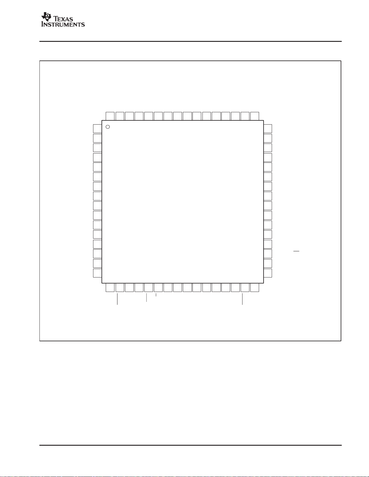
PIN CONFIGURATION
Top View TQFP
SDOUTA
BCKOA
LRCKOA
TDMIA
BCKIA
LRCKIA
SDINA
DGND
IFMTA0
IFMTA1
IFMTA2
OFMTA0
OFMTA1
OWLA0
OWLA1
BYPA
LGRPA0
LGRPA1
DDNA
DEMA0
DEMA1
MODEA0
MODEA1
MODEA2
64 63 62 61 60 59 58
1
2
3
4
5
6
7
8
9
10
11
12
13
14
15
16
VIOSDINB
57 56 55 54
SRC4184
LRCKIB
BCKIB
TDMIB
LRCKOB
BCKOB
52 51 50 49
SDOUTB
48
47
46
45
44
43
42
41
40
39
38
37
36
35
34
33
IFMTB0
IFMTB1
IFMTB2
OFMTB0
OFMTB1
OWLB0
OWLB1
BYPB
LGRPB0
LGRPB1
DDNB
DEMB0
DEMB1 (CDOUT)
MODEB0 (CS)
MODEB1 (CCLK)
MODEB2 (CDIN)
17 18 19 20 21 22 23 24 25 26 275328 29 30 31 32
H/S
RDYA
RATIOA
MUTEA
RST
RCKIA
DGND
VDD33
VDD33
VDD18
REGEN
RCKIB
VDD18
RDYB
MUTEB
RATIOB
5
Page 6
"#$%#
www.ti.com
SBFS026B − JUNE 2004 − REVISED SEPTEMBER 2007
PIN DESCRIPTIONS
PIN # NAME I/O DESCRIPTION
1 IFMTA0 Input SRC A Audio Input Data Format
2 IFMTA1 Input SRC A Audio Input Data Format
3 IFMTA2 Input SRC A Audio Input Data Format
4 OFMTA0 Input SRC A Audio Output Data Format
5 OFMTA1 Input SRC A Audio Output Data Format
6 OWLA0 Input SRC A Audio Output Data Word Length
7 OWLA1 Input SRC A Audio Output Data Word Length
8 BYPA Input SRC A Bypass Mode (Active High)
9 LGRPA0 Input SRC A Low Group Delay Mode
10 LGRPA1 Input SRC A Low Group Delay Mode
11 DDNA Input SRC A Direct Downsampling Mode (Active High)
12 DEMA0 Input SRC A Digital De-Emphasis Filter Mode
13 DEMA1 Input SRC A Digital De-Emphasis Filter Mode
14 MODEA0 Input SRC A Serial Port Mode
15 MODEA1 Input SRC A Serial Port Mode
16 MODEA2 Input SRC A Serial Port Mode
17 RATIOA Output SRC A Ratio Flag
18 RDYA Output SRC A Ready Flag (Active Low)
19 MUTEA Input SRC A Output Soft Mute
20 RCKIA Input SRC A Reference Clock
21 RST Input Reset and Power-Down (Active Low)
22 H/S Input Control Mode (0 = Software, 1 = Hardware)
23 DGND Ground Digital Ground
24, 25 VDD33 Power Core Supply, +3.3V. Required when REGEN is high. When REGEN is low, VDD33 must be left unconnected.
26 REGEN Input Voltage Regulator Enable (Active High)
27, 28 VDD18 Power Core Supply, +1.8V. Required when REGEN is low. When REGEN is high, VDD18 must be left unconnected.
29 RCKIB Input SRC B Reference Clock
30 MUTEB Input SRC B Output Soft Mute
31 RDYB Output SRC B Ready Flag (Active Low)
32 RATIOB Output SRC B Ratio Flag
33 MODEB2 or CDIN Input SRC B Serial Port Mode
34 MODEB1 or CCLK Input SRC B Serial Port Mode
35 MODEB0 or CS Input SRC B Serial Port Mode
36 DEMB1 or CDOUT I/O SRC B Digital De-Emphasis Filter Mode
37 DEMB0 Input SRC B Digital De-Emphasis Filter Mode
38 DDNB Input SRC B Direct Downsampling Mode (Active High)
39 LGRPB1 Input SRC B Low Group Delay Mode
40 LGRPB0 Input SRC B Low Group Delay Mode
41 BYPB Input SRC B Bypass Mode (Active High)
42 OWLB1 Input SRC B Audio Output Data Word Length
43 OWLB0 Input SRC B Audio Output Data Word Length
44 OFMTB1 Input SRC B Audio Output Data Format
45 OFMTB0 Input SRC B Audio Output Data Format
46 IFMTB2 Input SRC B Audio Input Data Format
47 IFMTB1 Input SRC B Audio Input Data Format
48 IFMTB0 Input SRC B Audio Input Data Format
49 SDOUTB Output SRC B Audio Output Data
50 BCKOB I/O SRC B Audio Output Bit Clock
51 LRCKOB I/O SRC B Audio Output Left/Right or Word Clock
52 TDMIB Input SRC B TDM Input Data (TDM Format Only)
53 BCKIB I/O SRC B Audio Input Bit Clock
54 LRCKIB I/O SRC B Audio Input Left/Right or Word Clock
55 SDINB Input SRC B Audio Input Data
56 V
57 DGND Ground Digital Ground
58 SDINA Input SRC A Audio Input Data
59 LRCKIA I/O SRC A Audio Input Left/Right or Word Clock
60 BCKIA I/O SRC A Audio Input Bit Clock
61 TDMIA Input SRC A TDM Input Data (TDM Format Only)
62 LRCKOA I/O SRC A Audio Output Left/Right or Word Clock
63 BCKOA I/O SRC A Audio Output Bit Clock
64 SDOUTA Output SRC A Audio Output Data
(1)
Disabled in Software control mode.
(2)
Disabled in Hardware control mode.
IO
Power Digital I/O Supply, +1.65V to +3.6V
(1)
(1)
(1)
(1)
(1)
(1)
(1)
(1)
(1)
(1)
(1)
(1)
(1)
or SPI Port Serial Data Input
(1)
or SPI Port Data Clock
(1)
or SPI Port Chip Select (Active Low)
(1)
(1)
(1)
(1)
(1)
(1)
(1)
(1)
(1)
(1)
(2)
(1)
or SPI Port Serial Data Output
(1)
(1)
(1)
(1)
(2)
(2)
(2)
6
Page 7
www.ti.com
SBFS026B − JUNE 2004 − REVISED SEPTEMBER 2007
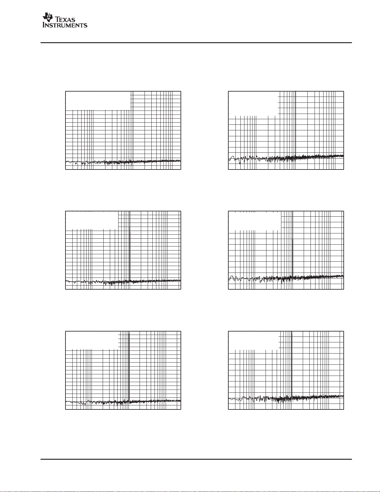
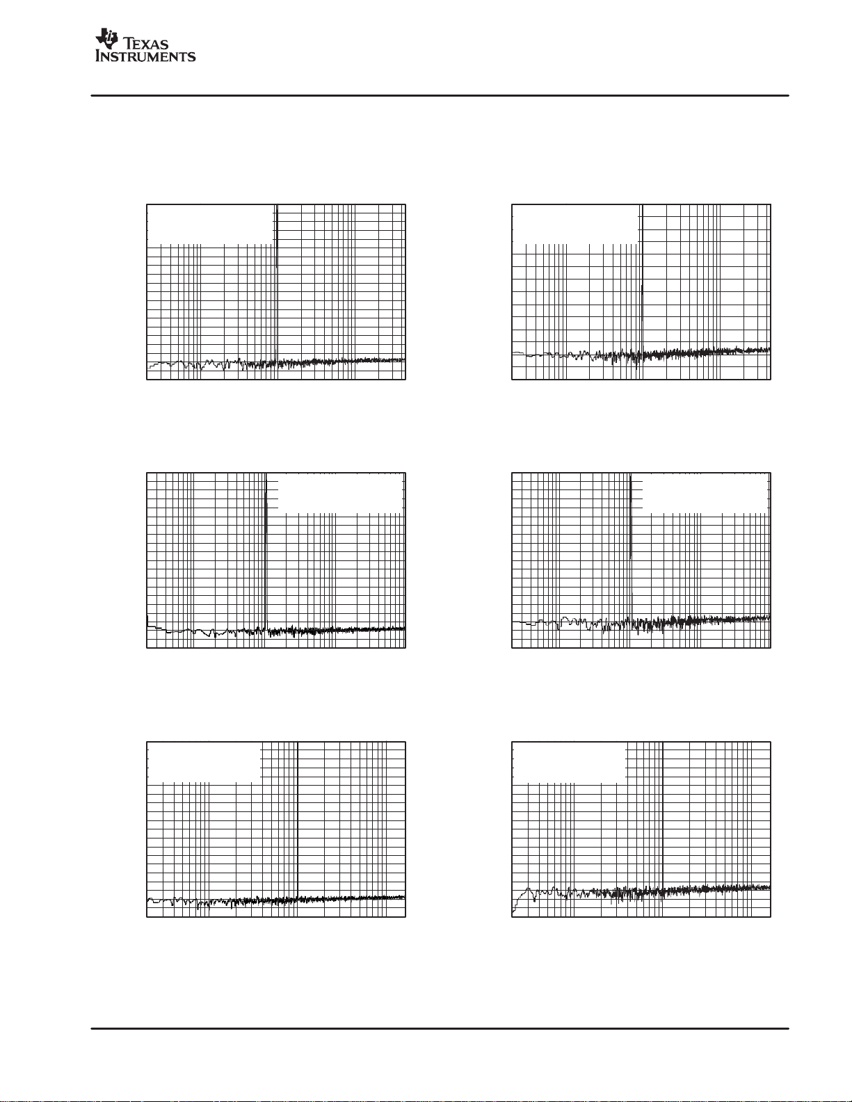
TYPICAL CHARACTERISTICS
All specifications at TA = +25°C, VDD33 = +3.3V, VIO = +3.3V, REGEN = High, and VDD18 floating, unless otherwise noted.
"#$%#
0
f
−
10
−
20
−
30
−
40
−
50
−
60
−
70
−
80
−
90
−
100
−
110
−
120
−
130
Amplitude (dBFS)
−
140
−
150
−
160
−
170
−
180
−
190
−
200
= 32kHz:32kHz
sIN:fsOUT
(asynchronous)
= 1kHz with 0dBFS Amplitude
f
IN
20 100 1k 16k10k
Frequency (Hz)
FFT PLOT
FFT PLOT
0
f
−
10
−
20
−
30
−
40
−
50
−
60
−
70
−
80
−
90
−
100
−
110
−
120
−
130
Amplitude (dBFS)
−
140
−
150
−
160
−
170
−
180
−
190
−
200
= 32kHz:44.1kHz
sIN:fsOUT
=1kHz
f
IN
with 0dBFS Amplitude
20 100 1k 22k10k
Frequency (Hz)
−
60
f
−
70
−
80
−
90
−
100
−
110
−
120
−
130
−
140
−
150
Amplitude (dBFS)
−
160
−
170
−
180
−
190
−
200
= 32kHz:32kHz
sIN:fsOUT
(asynchronous)
=1kHz
f
IN
with−60dBFS Amplitude
20 100 1k 16k10k
Frequency (Hz)
FFT PLOT
FFT PLOT
−
60
f
−
70
−
80
−
90
−
100
−
110
−
120
−
130
−
140
−
150
Amplitude (dBFS)
−
160
−
170
−
180
−
190
−
200
= 32kHz:44.1kHz
sIN:fsOUT
=1kHz
f
IN
with−60dBFS Amplitude
20 100 1k 22k10k
Frequency (Hz)
0
f
−
10
−
20
−
30
−
40
−
50
−
60
−
70
−
80
−
90
−
100
−
110
−
120
−
130
Amplitude (dBFS)
−
140
−
150
−
160
−
170
−
180
−
190
−
200
= 32kHz:48kHz
sIN:fsOUT
=1kHz
f
IN
with 0dBFS Amplitude
20 100 1k 24k10k
Frequency (Hz)
FFT PLOT
−
60
f
= 32kHz:48kHz
sIN:fsOUT
−
70
=1kHz
f
IN
−
80
with−60dBFS Amplitude
−
90
−
100
−
110
−
120
−
130
−
140
−
150
Amplitude (dBFS)
−
160
−
170
−
180
−
190
−
200
20 100 1k 24k10k
Frequency (Hz)
FFT PLOT
7
Page 8
"#$%#
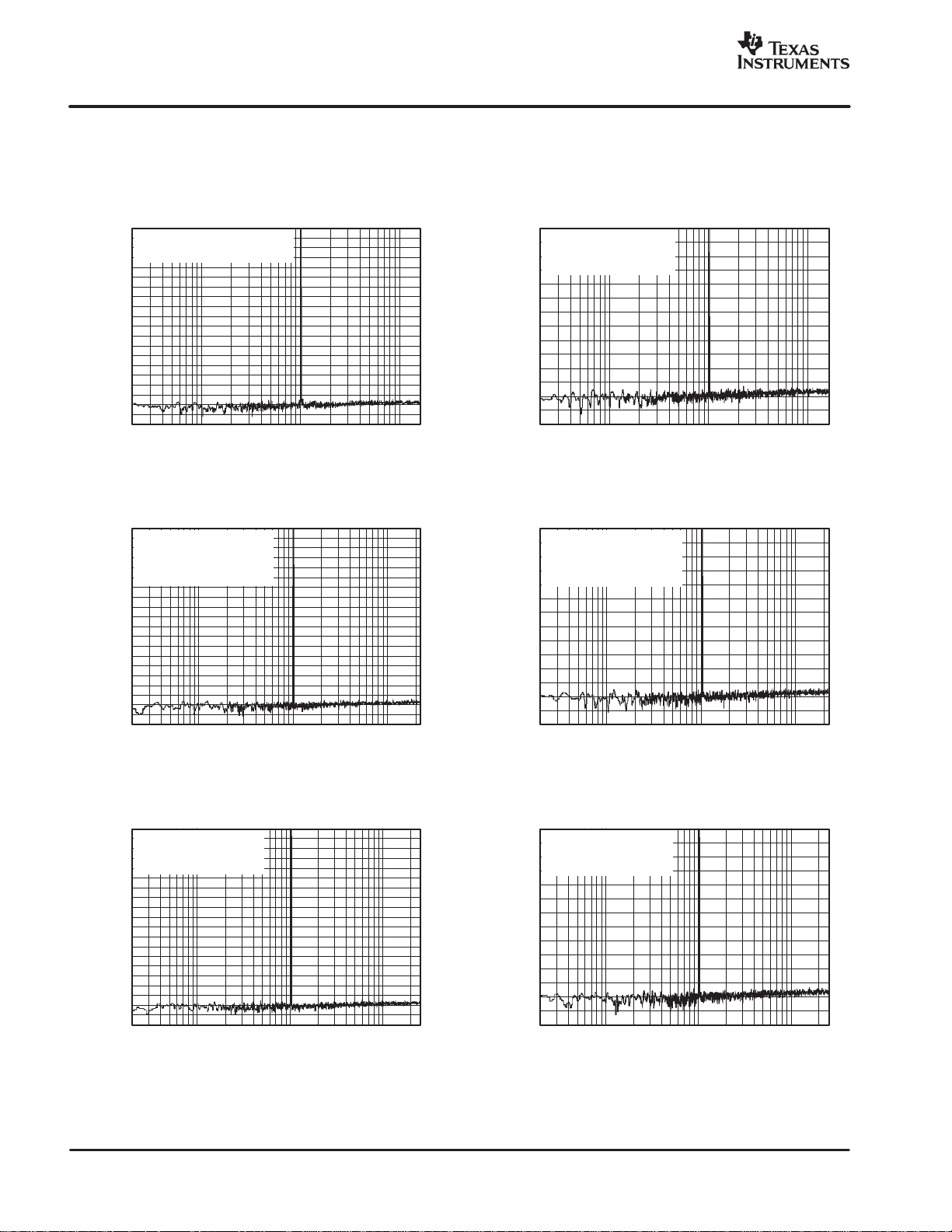
SBFS026B − JUNE 2004 − REVISED SEPTEMBER 2007
TYPICAL CHARACTERISTICS (continued)
All specifications at TA = +25°C, VDD33 = +3.3V, VIO = +3.3V, REGEN = High, and VDD18 floating, unless otherwise noted.
www.ti.com
0
f
−
10
−
20
−
30
−
40
−
50
−
60
−
70
−
80
−
90
−
100
−
110
−
120
−
130
Amplitude (dBFS)
−
140
−
150
−
160
−
170
−
180
−
190
−
200
= 44.1kHz:32kHz
sIN:fsOUT
= 1kHz with 0dBFS Amplitude
f
IN
20 100 1k 16k10k
Frequency (Hz)
FFT PLOT
FFT PLOT
0
f
−
10
−
20
−
30
−
40
−
50
−
60
−
70
−
80
−
90
−
100
−
110
−
120
−
130
Amplitude (dBFS)
−
140
−
150
−
160
−
170
−
180
−
190
−
200
= 44.1kHz:44.1kHz
sIN:fsOUT
(asynchronous)
=1kHz
f
IN
with 0dBFS Amplitude
20 100 1k 22k10k
Frequency (Hz)
−
60
f
−
70
−
80
−
90
−
100
−
110
−
120
−
130
−
140
−
150
Amplitude (dBFS)
−
160
−
170
−
180
−
190
−
200
= 44.1kHz:32kHz
sIN:fsOUT
=1kHz
f
IN
with−60dBFS Amplitude
20 100 1k 16k10k
Frequency (Hz)
FFT PLOT
FFT PLOT
−
60
f
= 44.1kHz:44.1kHz
sIN:fsOUT
−
70
(asynchronous)
−
80
=1kHz
f
IN
−
90
with−60dBFS Amplitude
−
100
−
110
−
120
−
130
−
140
−
150
Amplitude (dBFS)
−
160
−
170
−
180
−
190
−
200
20 100 1k 22k10k
Frequency (Hz)
0
f
−
10
−
20
−
30
−
40
−
50
−
60
−
70
−
80
−
90
−
100
−
110
−
120
−
130
Amplitude (dBFS)
−
140
−
150
−
160
−
170
−
180
−
190
−
200
= 44.1kHz:48kHz
sIN:fsOUT
=1kHz
f
IN
with 0dBFS Amplitude
20 100 1k 24k10k
Frequency (Hz)
FFT PLOT
−
60
f
= 44.1kHz:48kHz
sIN:fsOUT
−
70
=1kHz
f
IN
−
80
with−60dBFS Amplitude
−
90
−
100
−
110
−
120
−
130
−
140
−
150
Amplitude (dBFS)
−
160
−
170
−
180
−
190
−
200
20 100 1k 24k10k
FFT PLOT
Frequency (Hz)
8
Page 9
www.ti.com
SBFS026B − JUNE 2004 − REVISED SEPTEMBER 2007
TYPICAL CHARACTERISTICS (continued)
All specifications at TA = +25°C, VDD33 = +3.3V, VIO = +3.3V, REGEN = High, and VDD18 floating, unless otherwise noted.
"#$%#
0
f
−
10
−
20
−
30
−
40
−
50
−
60
−
70
−
80
−
90
−
100
−
110
−
120
−
130
Amplitude (dBFS)
−
140
−
150
−
160
−
170
−
180
−
190
−
200
= 44.1kHz:88.2kHz
sIN:fsOUT
=1kHz
f
IN
with 0dBFS Amplitude
20 100 1k 44k10k
Frequency (Hz)
FFT PLOT
FFT PLOT
0
−
10
−
20
−
30
−
40
−
50
−
60
−
70
−
80
−
90
−
100
−
110
−
120
−
130
Amplitude (dBFS)
−
140
−
150
−
160
−
170
−
180
−
190
−
200
f
sIN:fsOUT
20 100 1k 96k10k
Frequency (Hz)
= 44.1kHz:192kHz
=1kHz
f
with 0dBFS Amplitude
IN
−
60
f
= 44.1kHz:88.2kHz
sIN:fsOUT
−
70
=1kHz
f
IN
−
80
with−60dBFS Amplitude
−
90
−
100
−
110
−
120
−
130
−
140
−
150
Amplitude (dBFS)
−
160
−
170
−
180
−
190
−
200
20 100 1k 44k10k
Frequency (Hz)
FFT PLOT
FFT PLOT
−
60
−
70
−
80
−
90
−
100
−
110
−
120
−
130
−
140
−
150
Amplitude (dBFS)
−
160
−
170
−
180
−
190
−
200
f
sIN:fsOUT
20 100 1k 96k10k
Frequency (Hz)
= 44.1kHz:192kHz
=1kHz
f
with−60dBFS Amplitude
IN
0
f
−
10
−
20
−
30
−
40
−
50
−
60
−
70
−
80
−
90
−
100
−
110
−
120
−
130
Amplitude (dBFS)
−
140
−
150
−
160
−
170
−
180
−
190
−
200
= 48kHz:32kHz
sIN:fsOUT
=1kHz
f
IN
with 0dBFS Amplitude
20 100 1k 16k10k
Frequency (Hz)
FFT PLOT
−
60
f
= 48kHz:32kHz
sIN:fsOUT
−
70
=1kHz
f
IN
−
80
with−60dBFS Amplitude
−
90
−
100
−
110
−
120
−
130
−
140
−
150
Amplitude (dBFS)
−
160
−
170
−
180
−
190
−
200
20 100 1k 16k10k
Frequency (Hz)
FFT PLOT
9
Page 10
"#$%#
SBFS026B − JUNE 2004 − REVISED SEPTEMBER 2007
TYPICAL CHARACTERISTICS (continued)
All specifications at TA = +25°C, VDD33 = +3.3V, VIO = +3.3V, REGEN = High, and VDD18 floating, unless otherwise noted.
www.ti.com
0
f
−
10
−
20
−
30
−
40
−
50
−
60
−
70
−
80
−
90
−
100
−
110
−
120
−
130
Amplitude (dBFS)
−
140
−
150
−
160
−
170
−
180
−
190
−
200
= 48kHz:44.1kHz
sIN:fsOUT
=1kHz
f
IN
with 0dBFS Amplitude
20 100 1k 22k10k
Frequency (Hz)
FFT PLOT
FFT PLOT
0
f
−
10
−
20
−
30
−
40
−
50
−
60
−
70
−
80
−
90
−
100
−
110
−
120
−
130
Amplitude (dBFS)
−
140
−
150
−
160
−
170
−
180
−
190
−
200
= 48kHz:48kHz
sIN:fsOUT
(asynchronous)
=1kHz
f
IN
with 0dBFS Amplitude
20 100 1k 24k10k
Frequency (Hz)
−
60
f
= 48kHz:44.1kHz
sIN:fsOUT
−
70
=1kHz
f
IN
−
80
with−60dBFS Amplitude
−
90
−
100
−
110
−
120
−
130
−
140
−
150
Amplitude (dBFS)
−
160
−
170
−
180
−
190
−
200
20 100 1k 22k10k
Frequency (Hz)
FFT PLOT
FFT PLOT
−
60
f
= 48kHz:48kHz
sIN:fsOUT
−
70
(asynchronous)
−
80
=1kHz
f
IN
−
90
with−60dBFS Amplitude
−
100
−
110
−
120
−
130
−
140
−
150
Amplitude (dBFS)
−
160
−
170
−
180
−
190
−
200
20 100 1k 24k10k
Frequency (Hz)
10
0
f
−
10
−
20
−
30
−
40
−
50
−
60
−
70
−
80
−
90
−
100
−
110
−
120
−
130
Amplitude (dBFS)
−
140
−
150
−
160
−
170
−
180
−
190
−
200
= 48kHz:96kHz
sIN:fsOUT
=1kHz
f
IN
with 0dBFS Amplitude
20 100 1k 48k10k
Frequency (Hz)
FFT PLOT
−
60
f
= 48kHz:96kHz
sIN:fsOUT
−
70
=1kHz
f
IN
−
80
with−60dBFS Amplitude
−
90
−
100
−
110
−
120
−
130
−
140
−
150
Amplitude (dBFS)
−
160
−
170
−
180
−
190
−
200
20 100 1k 48k10k
Frequency (Hz)
FFT PLOT
Page 11
www.ti.com
SBFS026B − JUNE 2004 − REVISED SEPTEMBER 2007
TYPICAL CHARACTERISTICS (continued)
All specifications at TA = +25°C, VDD33 = +3.3V, VIO = +3.3V, REGEN = High, and VDD18 floating, unless otherwise noted.
"#$%#
0
−
10
−
20
−
30
−
40
−
50
−
60
−
70
−
80
−
90
−
100
−
110
−
120
−
130
Amplitude (dBFS)
−
140
−
150
−
160
−
170
−
180
−
190
−
200
f
sIN:fsOUT
with 0dBFS Amplitude
20 100 1k 96k10k
Frequency (Hz)
FFT PLOT
FFT PLOT
0
f
−
10
−
20
−
30
−
40
−
50
−
60
−
70
−
80
−
90
−
100
−
110
−
120
−
130
Amplitude (dBFS)
−
140
−
150
−
160
−
170
−
180
−
190
−
200
= 96kHz:44.1kHz
sIN:fsOUT
=1kHz
f
IN
with 0dBFS Amplitude
20 100 1k 22k10k
Frequency (Hz)
= 48kHz:192kHz
=1kHz
f
IN
−
60
−
70
−
80
−
90
−
100
−
110
−
120
−
130
−
140
−
150
Amplitude (dBFS)
−
160
−
170
−
180
−
190
−
200
f
sIN:fsOUT
with−60dBFS Amplitude
20 100 1k 96k10k
Frequency (Hz)
FFT PLOT
FFT PLOT
−
60
f
= 96kHz:44.1kHz
sIN:fsOUT
−
70
=1kHz
f
IN
−
80
with−60dBFS Amplitude
−
90
−
100
−
110
−
120
−
130
−
140
−
150
Amplitude (dBFS)
−
160
−
170
−
180
−
190
−
200
20 100 1k 22k10k
Frequency (Hz)
= 48kHz:192kHz
=1kHz
f
IN
0
f
−
10
−
20
−
30
−
40
−
50
−
60
−
70
−
80
−
90
−
100
−
110
−
120
−
130
Amplitude (dBFS)
−
140
−
150
−
160
−
170
−
180
−
190
−
200
= 96kHz:48kHz
sIN:fsOUT
=1kHz
f
IN
with 0dBFS Amplitude
20 100 1k 24k10k
Frequency (Hz)
FFT PLOT
−
60
f
= 96kHz:48kHz
sIN:fsOUT
−
70
=1kHz
f
IN
−
80
with−60dBFS Amplitude
−
90
−
100
−
110
−
120
−
130
−
140
−
150
Amplitude (dBFS)
−
160
−
170
−
180
−
190
−
200
20 100 1k 24k10k
Frequency (Hz)
FFT PLOT
11
Page 12
"#$%#
SBFS026B − JUNE 2004 − REVISED SEPTEMBER 2007
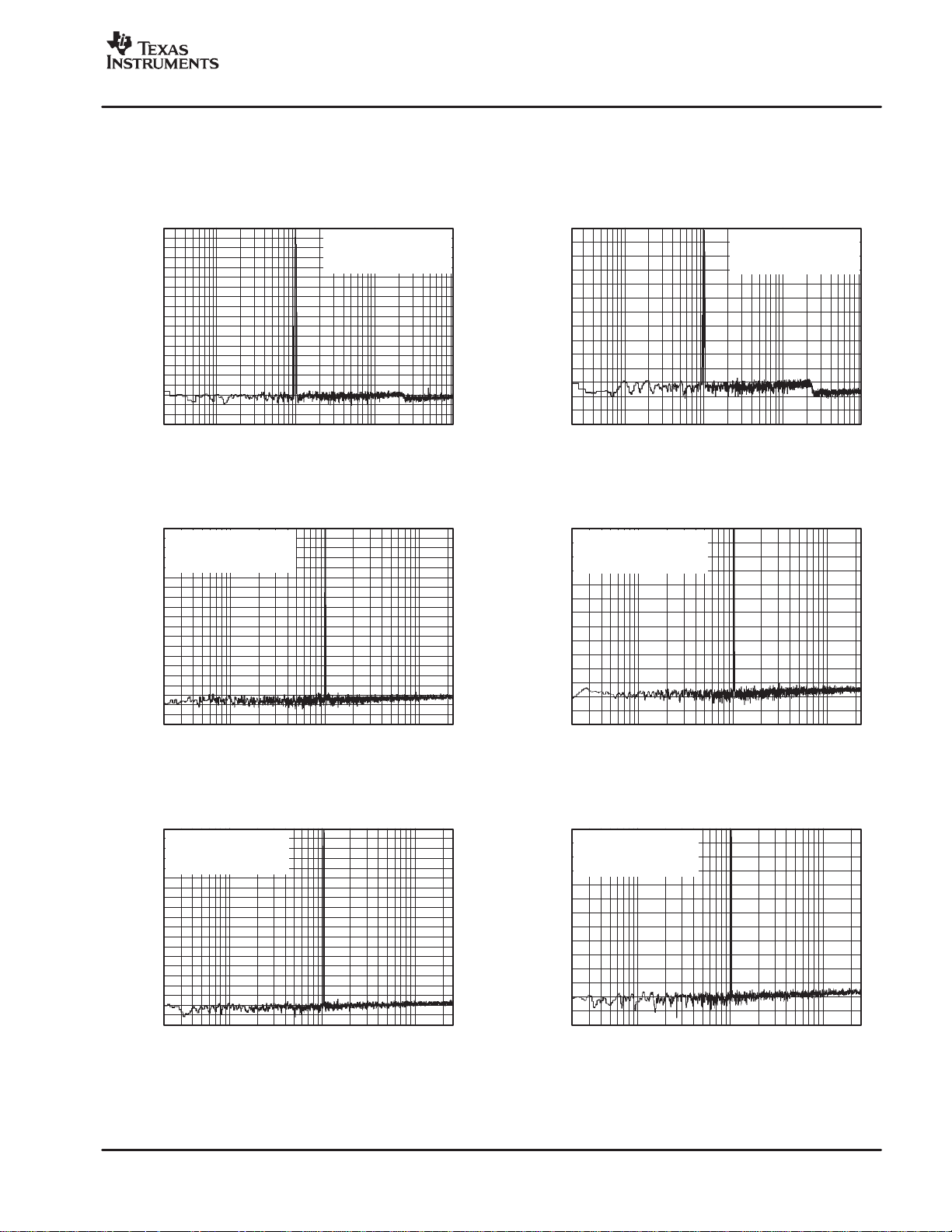
TYPICAL CHARACTERISTICS (continued)
All specifications at TA = +25°C, VDD33 = +3.3V, VIO = +3.3V, REGEN = High, and VDD18 floating, unless otherwise noted.
www.ti.com
0
f
−
10
−
20
−
30
−
40
−
50
−
60
−
70
−
80
−
90
−
100
−
110
−
120
−
130
Amplitude (dBFS)
−
140
−
150
−
160
−
170
−
180
−
190
−
200
= 96kHz:96kHz
sIN:fsOUT
(asynchronous)
=1kHz
f
IN
with 0dBFS Amplitude
20 100 1k 48k10k
Frequency (Hz)
FFT PLOT
FFT PLOT
0
−
10
−
20
−
30
−
40
−
50
−
60
−
70
−
80
−
90
−
100
−
110
−
120
−
130
Amplitude (dBFS)
−
140
−
150
−
160
−
170
−
180
−
190
−
200
20 100 1k 96k10k
Frequency (Hz)
f
= 96kHz:192kHz
sIN:fsOUT
with 0dBFS Amplitude
f
IN
=1kHz
−
60
f
= 96kHz:96kHz
sIN:fsOUT
−
70
(asynchronous)
−
80
=1kHz
f
IN
−
90
with−60dBFS Amplitude
−
100
−
110
−
120
−
130
−
140
−
150
Amplitude (dBFS)
−
160
−
170
−
180
−
190
−
200
20 100 1k 48k10k
Frequency (Hz)
FFT PLOT
FFT PLOT
−
60
−
70
−
80
−
90
−
100
−
110
−
120
−
130
−
140
−
150
Amplitude (dBFS)
−
160
−
170
−
180
−
190
−
200
20 100 1k 96k10k
Frequency (Hz)
f
= 96kHz:192kHz
sIN:fsOUT
with−60dBFS Amplitude
f
IN
=1kHz
12
0
f
−
10
−
20
−
30
−
40
−
50
−
60
−
70
−
80
−
90
−
100
−
110
−
120
−
130
Amplitude (dBFS)
−
140
−
150
−
160
−
170
−
180
−
190
−
200
= 192kHz:44.1kHz
sIN:fsOUT
=1kHz
f
IN
with 0dBFS Amplitude
20 100 1k 22k10k
Frequency (Hz)
FFT PLOT
−
60
f
= 192kHz:44.1kHz
sIN:fsOUT
−
70
=1kHz
f
IN
−
80
with−60dBFS Amplitude
−
90
−
100
−
110
−
120
−
130
−
140
−
150
Amplitude (dBFS)
−
160
−
170
−
180
−
190
−
200
20 100 1k 22k10k
Frequency (Hz)
FFT PLOT
Page 13
www.ti.com
SBFS026B − JUNE 2004 − REVISED SEPTEMBER 2007
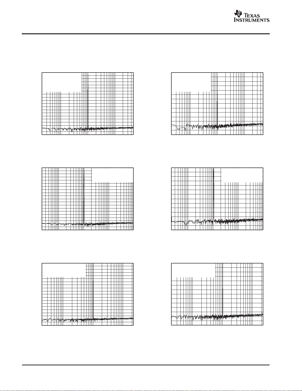
TYPICAL CHARACTERISTICS (continued)
All specifications at TA = +25°C, VDD33 = +3.3V, VIO = +3.3V, REGEN = High, and VDD18 floating, unless otherwise noted.
"#$%#
0
f
−
10
−
20
−
30
−
40
−
50
−
60
−
70
−
80
−
90
−
100
−
110
−
120
−
130
Amplitude (dBFS)
−
140
−
150
−
160
−
170
−
180
−
190
−
200
= 192kHz:48kHz
sIN:fsOUT
=1kHz
f
IN
with 0dBFS Amplitude
20 100 1k 24k10k
Frequency (Hz)
FFT PLOT
FFT PLOT
0
f
−
10
−
20
−
30
−
40
−
50
−
60
−
70
−
80
−
90
−
100
−
110
−
120
−
130
Amplitude (dBFS)
−
140
−
150
−
160
−
170
−
180
−
190
−
200
= 192kHz:96kHz
sIN:fsOUT
=1kHz
f
IN
with 0dBFS Amplitude
20 100 1k 48k10k
Frequency (Hz)
−
60
f
= 192kHz:48kHz
sIN:fsOUT
−
70
=1kHz
f
IN
−
80
with−60dBFS Amplitude
−
90
−
100
−
110
−
120
−
130
−
140
−
150
Amplitude (dBFS)
−
160
−
170
−
180
−
190
−
200
20 100 1k 24k10k
Frequency (Hz)
FFT PLOT
FFT PLOT
−
60
f
= 192kHz:96kHz
sIN:fsOUT
−
70
=1kHz
f
IN
−
80
with−60dBFS Amplitude
−
90
−
100
−
110
−
120
−
130
−
140
−
150
Amplitude (dBFS)
−
160
−
170
−
180
−
190
−
200
20 100 1k 48k10k
Frequency (Hz)
0
−
10
−
20
−
30
−
40
−
50
−
60
−
70
−
80
−
90
−
100
−
110
−
120
−
130
Amplitude (dBFS)
−
140
−
150
−
160
−
170
−
180
−
190
−
200
20 100 1k 96k10k
Frequency (Hz)
FFT PLOT
f
= 48kHz:192kHz
sIN:fsOUT
f
with 0dBFS Amplitude
=1kHz
IN
−
60
−
70
−
80
−
90
−
100
−
110
−
120
−
130
−
140
−
150
Amplitude (dBFS)
−
160
−
170
−
180
−
190
−
200
20 100 1k 96k10k
Frequency (Hz)
FFT PLOT
f
= 48kHz:192kHz
sIN:fsOUT
with−60dBFS Amplitude
f
IN
=1kHz
13
Page 14

"#$%#
SBFS026B − JUNE 2004 − REVISED SEPTEMBER 2007
TYPICAL CHARACTERISTICS (continued)
All specifications at TA = +25°C, VDD33 = +3.3V, VIO = +3.3V, REGEN = High, and VDD18 floating, unless otherwise noted.
www.ti.com
0
f
−
10
−
20
−
30
−
40
−
50
−
60
−
70
−
80
−
90
−
100
−
110
−
120
−
130
Amplitude (dBFS)
−
140
−
150
−
160
−
170
−
180
−
190
−
200
= 44.1kHz:48kHz
sIN:fsOUT
= 20kHz with 0dBFS Amplitude
f
IN
20 100 1k 24k10k
Frequency (Hz)
FFT PLOT
FFT PLOT
0
f
−
10
−
20
−
30
−
40
−
50
−
60
−
70
−
80
−
90
−
100
−
110
−
120
−
130
Amplitude (dBFS)
−
140
−
150
−
160
−
170
−
180
−
190
−
200
= 48kHz:48kHz (asynchronous)
sIN:fsOUT
= 20kHz with 0dBFS Amplitude
f
IN
20 100 1k 24k10k
Frequency (Hz)
0
f
−
10
−
20
−
30
−
40
−
50
−
60
−
70
−
80
−
90
−
100
−
110
−
120
−
130
Amplitude (dBFS)
−
140
−
150
−
160
−
170
−
180
−
190
−
200
= 48kHz:44.1kHz
sIN:fsOUT
= 20kHz with 0dBFS Amplitude
f
IN
20 100 1k 22k10k
Frequency (Hz)
FFT PLOT
FFT PLOT
0
f
−
10
−
20
−
30
−
40
−
50
−
60
−
70
−
80
−
90
−
100
−
110
−
120
−
130
Amplitude (dBFS)
−
140
−
150
−
160
−
170
−
180
−
190
−
200
= 48kHz:96kHz
sIN:fsOUT
= 20kHz with 0dBFS Amplitude
f
IN
20 100 1k 48k10k
Frequency (Hz)
14
0
f
−
10
−
20
−
30
−
40
−
50
−
60
−
70
−
80
−
90
−
100
−
110
−
120
−
130
Amplitude (dBFS)
−
140
−
150
−
160
−
170
−
180
−
190
−
200
= 96kHz:48kHz
sIN:fsOUT
= 20kHz with 0dBFS Amplitude
f
IN
20 100 1k 24k10k
Frequency (Hz)
FFT PLOT
0
f
−
10
−
20
−
30
−
40
−
50
−
60
−
70
−
80
−
90
−
100
−
110
−
120
−
130
Amplitude (dBFS)
−
140
−
150
−
160
−
170
−
180
−
190
−
200
= 192kHz:192kHz (asynchronous)
sIN:fsOUT
= 80kHz with 0dBFS Amplitude
f
IN
20 100 1k 96k10k
Frequency (Hz)
FFT PLOT
Page 15

www.ti.com
SBFS026B − JUNE 2004 − REVISED SEPTEMBER 2007
TYPICAL CHARACTERISTICS (continued)
All specifications at TA = +25°C, VDD33 = +3.3V, VIO = +3.3V, REGEN = High, and VDD18 floating, unless otherwise noted.
"#$%#
−
120
−
122
f
= 44.1kHz:48kHz
sIN:fsOUT
−
124
=1kHz
f
IN
−
126
−
BW = 10Hzto f
128
−
130
−
132
−
134
−
136
−
138
−
140
−
142
−
144
THD+N (dB)
−
146
−
148
−
150
−
152
−
154
−
156
−
158
−
160
−
−
140 0
120−100−80−60−40−20
sOUT
/2
Input Amplitude (dBFS)
THD+N vs INPUT AMPLITUDE
THD+N vs INPUT AMPLITUDE
−
120
f
−
122
−
124
−
126
−
128
−
130
−
132
−
134
−
136
−
138
−
140
−
142
−
144
THD+N (dB)
−
146
−
148
−
150
−
152
−
154
−
156
−
158
−
160
−
140 0
= 48kHz:48kHz (asynchronous)
sIN:fsOUT
=1kHz
f
IN
BW = 10Hzto f
−
120−100−80−60−40−20
sOUT
/2
Input Amplitude (dBFS)
−
120
f
−
122
−
124
−
126
−
128
−
130
−
132
−
134
−
136
−
138
−
140
−
142
−
144
THD+N (dB)
−
146
−
148
−
150
−
152
−
154
−
156
−
158
−
160
−
140 0
= 48kHz:44.1kHz
sIN:fsOUT
=1kHz
f
IN
BW = 10Hzto f
−
120−100−80−60−40−20
sOUT
/2
Input Amplitude (dBFS)
THD+N vs INPUT AMPLITUDE
THD+N vs INPUT AMPLITUDE
−
120
−
f
122
−
124
−
126
−
128
−
130
−
132
−
134
−
136
−
138
−
140
−
142
−
144
THD+N (dB)
−
146
−
148
−
150
−
152
−
154
−
156
−
158
−
160
−
140 0
= 48kHz:96kHz
sIN:fsOUT
=1kHz
f
IN
BW = 10Hzto f
−
120−100−80−60−40−20
sOUT
/2
Input Amplitude (dBFS)
−
120
f
−
122
−
124
−
126
−
128
−
130
−
132
−
134
−
136
−
138
−
140
−
142
−
144
THD+N (dB)
−
146
−
148
−
150
−
152
−
154
−
156
−
158
−
160
−
140 0
= 96kHz:48kHz
sIN:fsOUT
=1kHz
f
IN
BW = 10Hzto f
−
120−100−80−60−40−20
sOUT
/2
Input Amplitude (dBFS)
THD+N vs INPUT AMPLITUDE
−
120
f
−
122
−
124
−
126
−
128
−
130
−
132
−
134
−
136
−
138
−
140
−
142
−
144
THD+N (dB)
−
146
−
148
−
150
−
152
−
154
−
156
−
158
−
160
−
140 0
= 96kHz:96kHz (asynchronous)
sIN:fsOUT
=1kHz
f
IN
BW = 10Hzto f
−
120−100−80−60−40−20
sOUT
/2
Input Amplitude (dBFS)
THD+N vs INPUT AMPLITUDE
15
Page 16

"#$%#
SBFS026B − JUNE 2004 − REVISED SEPTEMBER 2007
TYPICAL CHARACTERISTICS (continued)
All specifications at TA = +25°C, VDD33 = +3.3V, VIO = +3.3V, REGEN = High, and VDD18 floating, unless otherwise noted.
www.ti.com
−
120
f
−
122
−
124
−
126
−
128
−
130
−
132
−
134
−
136
−
138
−
140
−
142
−
144
THD+N (dB)
−
146
−
148
−
150
−
152
−
154
−
156
−
158
−
160
−
140 0
= 192kHz:192kHz (asynchronous)
sIN:fsOUT
=1kHz
f
IN
BW = 10Hzto f
−
120−100−80−60−40−20
sOUT
/2
Input Amplitude (dBFS)
THD+N vs INPUT FREQUENCY
THD+N vs INPUT AMPLITUDE
−
120
f
−
122
−
124
−
126
−
128
−
130
−
132
−
134
−
136
−
138
−
140
−
142
−
144
THD+N (dB)
−
146
−
148
−
150
−
152
−
154
−
156
−
158
−
160
= 48kHz:44.1kHz
sIN:fsOUT
Input Amplitude = 0dBFS
BW = 10Hz to f
sOUT
/2
20 100 1k 20k10k
Input Frequency (Hz)
−
120
f
−
122
−
124
−
126
−
128
−
130
−
132
−
134
−
136
−
138
−
140
−
142
−
144
THD+N (dB)
−
146
−
148
−
150
−
152
−
154
−
156
−
158
−
160
= 44.1kHz:48kHz
sIN:fsOUT
Input Amplitude = 0dBFS
BW = 10Hz to f
sOUT
/2
20 100 1k 20k10k
Input Frequency (Hz)
THD+N vs INPUT FREQUENCY
THD+N vs INPUT FREQUENCY
−
120
f
−
122
−
124
−
126
−
128
−
130
−
132
−
134
−
136
−
138
−
140
−
142
−
144
THD+N (dB)
−
146
−
148
−
150
−
152
−
154
−
156
−
158
−
160
= 48kHz:48kHz (asynchronous)
sIN:fsOUT
Input Amplitude = 0dBFS
BW = 10Hz to f
sOUT
/2
20 100 1k 20k10k
Input Frequency (Hz)
16
−
120
f
−
122
−
124
−
126
−
128
−
130
−
132
−
134
−
136
−
138
−
140
−
142
−
144
THD+N (dB)
−
146
−
148
−
150
−
152
−
154
−
156
−
158
−
160
= 48kHz:96kHz
sIN:fsOUT
Input Amplitude = 0dBFS
BW = 10Hz to f
sOUT
/2
20 100 1k 20k10k
Input Frequency (Hz)
THD+N vs INPUT FREQUENCY
−
120
f
−
122
−
124
−
126
−
128
−
130
−
132
−
134
−
136
−
138
−
140
−
142
−
144
THD+N (dB)
−
146
−
148
−
150
−
152
−
154
−
156
−
158
−
160
= 96kHz:48kHz
sIN:fsOUT
Input Amplitude = 0dBFS
BW = 10Hz to f
sOUT
/2
20 100 1k 20k10k
Input Frequency (Hz)
THD+N vs INPUT FREQUENCY
Page 17

www.ti.com
SBFS026B − JUNE 2004 − REVISED SEPTEMBER 2007
TYPICAL CHARACTERISTICS (continued)
All specifications at TA = +25°C, VDD33 = +3.3V, VIO = +3.3V, REGEN = High, and VDD18 floating, unless otherwise noted.
"#$%#
−
120
f
−
122
−
124
−
126
−
128
−
130
−
132
−
134
−
136
−
138
−
140
−
142
−
144
THD+N (dB)
−
146
−
148
−
150
−
152
−
154
−
156
−
158
−
160
= 96kHz:96kHz (asynchronous)
sIN:fsOUT
Input Amplitude = 0dBFS
BW = 10Hz to f
sOUT
/2
20 100 1k 40k10k
Input Frequency (Hz)
LINEARITY
THD+N vs INPUT FREQUENCY
0
f
−
10
−
20
−
30
−
40
−
50
−
60
−
70
−
80
−
90
−
100
−
110
Output Amplitude (dBFS)
−
120
−
130
−
140
−
150
−
150−130 0
= 32kHz:32kHz (asynchronous)
sIN:fsOUT
= 200Hz
f
IN
−
110−90−70−50−30−10
Input Amplitude (dBFS)
−
120
f
−
122
−
124
−
126
−
128
−
130
−
132
−
134
−
136
−
138
−
140
−
142
−
144
THD+N (dB)
−
146
−
148
−
150
−
152
−
154
−
156
−
158
−
160
= 192kHz:192kHz (asynchronous)
sIN:fsOUT
Input Amplitude = 0dBFS
BW = 10Hz to f
sOUT
/2
20 100 1k 80k10k
Input Frequency (Hz)
LINEARITY
THD+N vs INPUT FREQUENCY
0
f
−
10
−
20
−
30
−
40
−
50
−
60
−
70
−
80
−
90
−
100
−
110
Output Amplitude (dBFS)
−
120
−
130
−
140
−
150
−
150−130 0
= 48kHz:48kHz (asynchronous)
sIN:fsOUT
= 200Hz
f
IN
−
110−90−70−50−30−10
Input Amplitude (dBFS)
0
f
−
10
−
20
−
30
−
40
−
50
−
60
−
70
−
80
−
90
−
100
−
110
Output Amplitude (dBFS)
−
120
−
130
−
140
−
150
−
150−130 0
= 96kHz:96kHz (asynchronous)
sIN:fsOUT
= 200Hz
f
IN
−
110−90−70−50−30−10
Input Amplitude (dBFS)
LINEARITY
0
f
−
10
−
20
−
30
−
40
−
50
−
60
−
70
−
80
−
90
−
100
−
110
Output Amplitude (dBFS)
−
120
−
130
−
140
−
150
−
150−130 0
= 192kHz:192kHz (asynchronous)
sIN:fsOUT
= 200Hz
f
IN
−
110−90−70−50−30−10
Input Amplitude (dBFS)
LINEARITY
17
Page 18

"#$%#
5
SBFS026B − JUNE 2004 − REVISED SEPTEMBER 2007
TYPICAL CHARACTERISTICS (continued)
All specifications at TA = +25°C, VDD33 = +3.3V, VIO = +3.3V, REGEN = High, and VDD18 floating, unless otherwise noted.
www.ti.com
0
−
10
−
20
−
30
−
40
−
50
−
60
−
70
−
80
−
90
−
100
−
110
Output Amplitude (dBFS)
−
120
−
130
f
sIN:fsOUT
−
140
Input Amplitude = 0dBFS
−
150
024 326 8 10 12 14 16 18 20 22 24 26 28 30
0
f
−
10
sIN:fsOUT
Input Amplitude = 0dBFS
−
20
−
30
−
40
−
50
−
60
−
70
−
80
−
90
−
100
−
110
Output Amplitude (dBFS)
−
120
−
130
−
140
−
150
0605 10152025303540455055
FREQUENCY RESPONSE
= 192kHz:32kHz
Input Frequency (kHz)
FREQUENCY RESPONSE
= 192kHz:96kHz
Input Frequency (kHz)
0
f
−
10
sIN:fsOUT
Input Amplitude = 0dBFS
−
20
−
30
−
40
−
50
−
60
−
70
−
80
−
90
−
100
−
110
Output Amplitude (dBFS)
−
120
−
130
−
140
−
150
0505 1015202530354045
0
f
sIN:fsOUT
−
0.005
−
0.010
−
0.015
−
0.020
Output Amplitude (dBFS)
−
0.025
−
0.030
01 15234567891011121314
FREQUENCY RESPONSE
= 192kHz:48kHz
Input Frequency (kHz)
PASS BANDRIPPLE
= 32kHz:32kHz (asynchronous)
Input Frequency(kHz)
18
0
f
= 48kHz:48kHz (asynchronous)
sIN:fsOUT
−
0.005
−
0.010
−
0.015
−
0.020
Output Amplitude (dBFS)
−
0.025
−
0.030
02 224 6 8 101214161820
PASS BANDRIPPLE
Input Frequency(kHz)
0
f
= 96kHz:96kHz (asynchronous)
sIN:fsOUT
−
0.005
−
0.010
−
0.015
−
0.020
Output Amplitude (dBFS)
−
0.025
−
0.030
0510 4
PASS BANDRIPPLE
15 20 25 30 35 40
Input Frequency (kHz)
Page 19

www.ti.com
SBFS026B − JUNE 2004 − REVISED SEPTEMBER 2007
TYPICAL CHARACTERISTICS (continued)
All specifications at TA = +25°C, VDD33 = +3.3V, VIO = +3.3V, REGEN = High, and VDD18 floating, unless otherwise noted.
"#$%#
0
f
= 192kHz:192kHz (asynchronous)
sIN:fsOUT
−
0.005
−
0.010
−
0.015
−
0.020
Output Amplitude (dBFS)
−
0.025
−
0.030
01020 9030 40 50 60 70 80
PASS BANDRIPPLE
Input Frequency (kHz)
19
Page 20

"#$%#
SBFS026B − JUNE 2004 − REVISED SEPTEMBER 2007
www.ti.com
PRODUCT OVERVIEW
The SRC4184 is a four-channel, asynchronous sample
rate converter (ASRC), implemented as two stereo
sections, referred to as SRC A and SRC B. Operation at
input and output sampling frequencies up to 212kHz is
supported, with a continuous input/output sampling ratio
range of 16:1 to 1:16. Excellent dynamic range and
THD+N are achieved by employing high-performance,
linear-phase digital filtering with better than 128dB of
image rejection. The digital filters provide settings for lower
latency processing, including low group delay options for
the interpolation filter and a direct downsampling option for
the decimation filter. Digital de-emphasis filtering is
included, supporting 32kHz, 44.1kHz, and 48kHz
sampling frequencies.
The audio input and output ports support standard audio
data formats, as well as a time division multiplexed (TDM)
format. Word lengths of 24-, 20-, 18-, and 16-bits are
supported. Input and output ports may operate in Slave
mode, deriving their word and bit clocks from external input
and output devices. Alternatively, one port may operate in
Master mode while the other remains in Slave mode. In
Master mode, the LRCK and BCK clocks are derived from
the reference clock inputs, either RCKIA or RCKIB. The
flexible configuration options for the input and output ports
allow connections to a variety of audio data converters,
digital audio interface devices, and digital signal
processors.
A bypass mode is included, which allows audio data to be
passed directly from the input port to the output port,
bypassing the ASRC function. The bypass option is useful
for passing through compressed or encoded audio data,
as well as non-audio data (that is, control or status
information).
A soft mute function is available for the SRC4184 in both
Hardware and Software modes. Digital output attenuation
is available only in Software mode. Both soft mute and
digital attenuation functions provide artifact-free
operation. The mute attenuation is typically −128dB, while
the digital attenuation function is adjustable from 0dB to
−127.5dB in 0.5dB steps.
The SRC4184 includes a four-wire SPI port, which is used
to access on-chip control and status registers in Software
mode. The SPI port facilitates interfacing to microprocessors or digital signal processors that support synchronous
serial peripherals. In Hardware mode, dedicated control
pins are provided for the majority of the SRC4184
functions. These pins can be hard-wired or driven by logic
or host control.
FUNCTIONAL BLOCK DIAGRAM
Figure 1 shows a functional block diagram of the
SRC4184. The SRC4184 is segmented into two stereo
SRC sections, referred to as SRC A and SRC B. Each
section can operate independently from the other. Each
section has individual sets of configuration pins in
Hardware mode, an d separate banks of control and status
registers in Software mode.
LRCKIA
BCKIA
SDINA
RCKIA
IFMTA0
IFMTA1
IFMTA2
OFMTA0
OFMTA1
OWLA0
OWLA1
BYPA
LRCKIB
BCKIB
SDINB
RCKIB
Input
Serial
Port
Control
SRCA
Input
Serial
Port
Digital
De−Emphasis and
Interpolation Filters
LGRPA 0
LGRPA 1
DDNA
DEMA0
DEMA1
MODEA0
MODEA1
MODEA2
MUTEA
Digital
De−Emphasis and
Interpolation Filters
Re−Sampler
f
sIN
f
sIN
Rate
Estimator
Re−Sampler
Rate
Estimator
Decimation
f
sOUT
RDYA
RATIOA
DEMB1 (CDOUT)
MODEB0(CS)
MODEB1(CCLK)
MODEB2 (CDIN)
Decimation
f
sOUT
RDYB
RATIOB
Figure 1. Functional Block Diagram
Digital
Filter
Digital
Filter
LGRPB0
LGRPB1
DDNB
DEMB0
MUTEB
Output
Serial
Port
Control
SRC B
SPI Port
and
Reset
Output
Serial
Port
LRCKOA
BCKOA
SDOUTA
TDMIA
IFMTB0
IFMTB1
IFMTB2
OFMTB0
OFMTB1
OWLB0
OWLB1
BYPB
H/S
RST
LRCKOB
BCKOB
SDOUTB
TDMIB
V
IO
DGND
VDD18 (2)
VDD33 (2)
DGND
REGEN
20
Page 21

www.ti.com
"#$%#
SBFS026B − JUNE 2004 − REVISED SEPTEMBER 2007
Operation for SRC A and SRC B is identical. Audio data
is received at the input serial port, clocked by either the
audio source device in Slave mode, or by the SRC4184 in
Master mode. The output port data is clocked by either the
audio output device in Slave mode, or by the SRC4184 in
Master mode. The input data is passed through
interpolation filters that upsample the data, which is then
passed on to the re-sampler. The rate estimator compares
the input and output sampling frequencies by comparing
LRCKI, LRCKO, and a reference clock. The results of the
rate estimation are utilized to configure the re-sampler
coefficients and data pointers.
The output of the re-sampler is passed on to either the
decimation filter or direct downsampler function. The
decimation filter performs downsampling and anti-alias
filtering functions, and is required when the output
sampling frequency is equal to or lower than the input
sampling frequency. The direct downsampler function
does not provide any filtering, and may be used in cases
when the output sampling frequency is greater than the
input sampling frequency. The advantage of the direct
downsampling function is a significant reduction in the
group delay associated with the decimation function,
allowing lower latency processing.
REFERENCE CLOCK
The SRC4184 includes two reference clock inputs, one
each for SRC A and SRC B. The reference clocks are
applied at the RCKIA (pin 20) and RCKIB (pin 29) inputs,
respectively. The reference clock is required for the rate
estimator function, as well as for the input or output serial
ports when configured in Master mode.
Figure 2 illustrates the reference clock connections and
requirements for the SRC4184. When either the input or
output port is configured in Master mode, the reference
clock may operate at 128f
desired sampling rate for the Master mode port. When both
the input and output port are configured in Slave mode, the
, 256fs, or 512fs, where fs is the
s
reference clock does not have to be a multiple of the input
or output sampling rates. The maximum reference clock
input frequency is 50MHz for RCKIA and RCKIB.
SRC4184
RCKI1
Clock Source(s)
RCKI
RCKI2
20
From External
50MHz Max
t
RCKIH
t
RCKIP
29
t
>20nsmin
RCKIP
t
>0.4t
t
RCKIL
RCKIH
t
RCKIL
>0.4t
RCKIP
RCKIP
Figure 2. Reference Clock Input Connections and
Timing Requirements
RESET AND POWER-DOWN OPERATION
The SRC4184 may be reset using the RST input (pin 21).
There is no internal power-on reset, so the user should
force a reset sequence after power-up in order to initialize
the device. In order to force a reset, the reference clock
inputs must be active, with external clock sources
supplying a valid reference clock signal (refer to Figure 2).
The user must assert RST
then bring RST
high again to force a reset. The reset
function affects both SRC A and SRC B. Figure 3 shows
the reset timing for the SRC4184.
In Software mode, there is a 500ms delay after the RST
rising edge due to internal logic requirements. The
customer should wait a minimum 500ms after the RST
rising edge before attempting to write to the SPI port of the
SRC4184 in Software mode.
low for a minimum of 500ns and
RCKI
RST
t
> 500ns
RSTL
Figure 3. Reset Pulsewidth Requirement
21
Page 22

"#$%#
SBFS026B − JUNE 2004 − REVISED SEPTEMBER 2007
www.ti.com
The SRC4184 also supports two power-down modes. The
entire SRC4184 may be powered down by forcing and
holding the RST input low. This is referred to as a Hard
Power-Down, and the SRC4184 consumes the least
amount of power in this mode.
In Software mode, there is an additional Soft Power-Down
available, utilizing the PDN
Power-Down is enabled when the PDN
bit in Control Register 1. Soft
bit is set to 0. Since
SRC A and SRC B have their own separate register banks,
they may be set to Soft Power-Down mode individually.
During Soft Power-Down, the SPI port and control
registers remain active for write and read access. The
internal voltage regulator also remains active if the
REGEN pin is forced high and +3.3V is applied at the
VDD33 pin.
Soft Power-Down mode consumes more power than the
Hard Power-Down mode. Refer to the Electrical
Characteristics tables in this data sheet for supply current
and power dissipation specifications for both modes.
Finally, there is one very important item to remember when
using Software mode. The default state of the PDN
bit is
0, meaning that the SRC4184 will default to the Soft
Power-Down state for both SRC A and SRC B after
power-up or reset. The user must set the PDN
bit to 1 for
both the SRC A and SRC B control register banks in order
to enable normal operation for both SRC sections.
AUDIO SERIAL PORT MODES
The SRC4184 supports seven serial port modes for the
SRC A and SRC B sections, which are shown in Table 1.
In Hardware mode, the audio port mode is selected using
the MODEA0 (pin 14), MODEA1 (pin 15), and MODEA2
(pin 16) inputs for SRC A, while the MODEB0 (pin 35),
MODEB1 (pin 34), and MODEB2 (pin 33) inputs are used
for SRC B.
In Software mode, the audio serial port modes are
selected using the MODE[2:0] bits in Control Register 1 for
the SRC A and SRC B register banks. The default setting
for Software mode is both input and output ports set to
Slave mode.
In Slave mode, the port LRCK and BCK clocks are
configured as inputs, and receive their clocks from an
external audio device. In Master mode, the LRCK and
BCK clocks are configured as outputs, being derived from
the reference clock input for the corresponding SRC
section, either RCKIA or RCKIB. Only one port can be set
to Master mode at any given time, as indicated in Table 1.
Table 1. Setting the Serial Port Modes (x = A or B)
MODEx2 MODEx1 MODEx0 SERIAL PORT MODE
0 0 0 Both Input and Output Ports are
0 0 1 Output Port is Master Mode with
0 1 0 Output Port is Master Mode with
0 1 1 Output Port is Master Mode with
1 0 0 Both Input and Output Ports are
1 0 1 Input Port is Master Mode with
1 1 0 Input Port is Master Mode with
1 1 1 Input Port is Master Mode with
Slave mode
RCKIx = 128f
RCKIx = 512f
RCKIx = 256f
Slave mode
RCKIx = 128f
RCKIx = 512f
RCKIx = 256f
S
S
S
S
S
S
INPUT PORT OPERATION
The audio input port is a three-wire synchronous serial
interface that may operate in either Slave or Master mode.
The SDINA (pin 58) and SDINB (pin 55) are the serial
audio data inputs for SRC A and SRC B, respectively.
Audio data is input at these pins in one of three standard
audio data formats: Philips I
Right-Justified. The audio data word length may be up to
24-bits for I
2
S and Left-Justified formats, while the
Right-Justified format supports 16-, 18-, 20-, or 24-bit data.
The audio data is always Binary Two’s Complement with
the MSB first. Refer to Figure 4 for the input data formats
and Figure 5 for the critical timing parameters, which are
also listed in the Electrical Characteristics table.
The bit clock is either an input or output at BCKIA (pin 60)
and BCKIB (pin 53). In Slave mode, the bit clock is
configured as an input pin, and may operate at rates from
32f
to 128fs,with a minimum of one clock cycle per data
s
bit. In Master mode, bit clock operates at a fixed rate of
64f
.
s
The left/right word clock, LRCKIA (pin 59) and LRCKIB
(pin 54), may be configured as an input or output pin. In
Slave mode, left/right clock is an input pin, while in Master
mode the left/right clock is an output pin. In either case, the
clock rate is equal to f
, the input sampling frequency . The
s
LRCKI duty cycle is fixed to 50% for Master mode
operation.
2
S, Left-Justified, or
22
Page 23

www.ti.com
"#$%#
SBFS026B − JUNE 2004 − REVISED SEPTEMBER 2007
LRCKI
BCKI
SDIN
LRCKI
BCKI
SDIN
LRCKI
BCKI
SDIN
Left Channel
MSB LSB LSBMSB
(a) Left−Justified Data Format
MSB MSB LSBLSB
(b) Right−Justified Data Format
MSB LSB MSB LSB
(c) I2SDataFormat
Right Channel
Figure 4. Input Data Formats
LRCKI
BCKI
SDIN
t
t
LRIS
LDIS
t
LDIH
t
SIH
t
SIL
Figure 5. Input Port Timing
Table 2 illustrates the data format selection for the input
port. For Hardware mode, the IFMTA0 (pin 1), IFMTA1
(pin 2), and IFMTA2 (pin 3) inputs are utilized to set the
1/f
S
input port data format for SRC A. IFMTB0 (pin 48), IFMTB1
(pin 47), and IFMTB2 (pin 46) are utilized to set the input
port data format for SRC B.
Table 2. Input Port Data Format Selection (x = A or B)
IFMTx2 IFMTx1 IFMTx0 INPUT PORT DA TA FORMAT
0 0 0 24-Bit Left-Justified
0 0 1 24-Bit I2S
0 1 0 Unused
0 1 1 Unused
1 0 0 16-Bit Right-Justified
1 0 1 18-Bit Right-Justified
1 1 0 20-Bit Right-Justified
1 1 1 24-Bit Right-Justified
In Software mode, the IFMT[2:0] bits in Control Register 3
are used to select the data format for the SRC A and
SRC B register banks. The default format is 24-Bit
Left-Justified.
23
Page 24

"#$%#
SBFS026B − JUNE 2004 − REVISED SEPTEMBER 2007
www.ti.com
OUTPUT PORT OPERATION
The audio output port is a four-wire synchronous serial
interface that may operate in either Slave or Master mode.
SDOUTA (pin 64) and SDOUTB (pin 49) are the serial
audio data outputs for SRC A and SRC B, respectively.
Audio data is output at these pins in one of four data
formats: Philips I
TDM. The audio data word length may be 16-, 18-, 20-, or
24-bits. For all word lengths, the data is triangular PDF
dithered from the internal 28-bit data path. The data
formats (with the exception of TDM mode) are shown in
Figure 7, while critical timing parameters are shown in
Figure 6 and listed in the Electrical Characteristics table.
The TDM format and timing are shown in Figure 15 and
Figure 16, respectively, while examples of standard TDM
configurations are shown in Figure 17 and Figure 18.
The bit clock is either input or output at BCKOA (pin 63)
and BCKOB (pin 50). In Slave mode, the bit clock is
configured as an input pin, and may operate at rates from
32f
to 128fs, with a minimum of one clock cycle for each
s
2
S, Left-Justified, Right-Justified, or
Left Channel
LRCKO
data bit. The exception is the TDM mode, where the BCKO
must operate at N × 64f
, where N is equal to the number
s
of SRC sections cascaded on the TDM bus. In Master
mode, the bit clock operates at a fixed rate of 64f
for all
s
data formats except TDM, where BCKO operates at the
reference clock frequency. Additional information
regarding TDM mode operation is included in the
Applications Information section of this data sheet.
LRCKO
t
SOH
BCKO
t
SOL
SDOUT
t
DOPD
t
DOH
Figure 6. Output Port Timing
Right Channel
BCKO
SDOUT
LRCKO
BCKO
SDOUT
LRCKO
BCKO
SDOUT
MSB LSB LSBMSB
(a)Left−JustifiedDataFormat
MSB MSB LSBLSB
(b) Right−Justified Data Format
MSB LSB MSB LSB
(c) I2SDataFormat
1/f
S
24
Figure 7. Output Data Formats
Page 25

www.ti.com
"#$%#
SBFS026B − JUNE 2004 − REVISED SEPTEMBER 2007
The left/right word clock, LRCKOA (pin 62) and LRCKOB
(pin 51), may be configured as an input or output pin. In
Slave mode, the left/right clock is an input pin, while in
Master mode it is an output pin. In either case, the clock
rate is equal to f
duty cycle is fixed to 50% for I
, the output sampling frequency . The clock
s
2
S, Left-Justified, and
Right-Justified formats in Master mode. The pulse width is
fixed to 32-bit clock cycles for the TDM format in Master
mode.
Table 3 illustrates data format selection for the output port.
In Hardware mode, the OFMTA0 (pin 4), OFMTA1 (pin 5),
OWLA0 (pin 6), and OWLA1 (pin 7) inputs are utilized to
set the output port data format and word length for SRC A.
The OFMTB0 (pin 45), OFMTB1 (pin 44), OWLB0 (pin 43),
and OWLB1 (pin 42) inputs are utilized to set the output
port data format and word length for SRC B.
Table 3. Output Port Data Format/Word Length
Selection (x = A or B)
OFMTx1 OFMTx0 OUTPUT PORT DATA FORMAT
0 0 Left-Justified
0 1 I2S
1 0 TDM
1 1 Right-Justified
OWLx1 OWLx0 OUTPUT PORT DATA WORD LENGTH
0 0 24 Bits
0 1 20 Bits
1 0 18 Bits
1 1 16 Bits
In Software mode, the OFMT[1:0] and OWL[1:0] bits in
Control Register 3 are used to select the data format and
word length for the SRC A and SRC B register banks. The
default format is Left-Justified data with a default word
length of 24-bits.
BYPASS MODE
passing through compressed or encoded audio data, as
well as non-audio data (that is, control or status
information).
INTERPOLATION FILTER GROUP DELAY
OPTIONS
The SRC4184 provides four group delay options for the
digital interpolation filter, as shown in Table 4. These
options allow the user to tailor the group delay for a given
application by selecting the number of input samples
buffered prior to the re-sampling function.
Table 4. Low Group Delay Configuration
(x = A or B)
LGRPx1 LGRPx0 BUFFER SIZE
0 0 64 Samples
0 1 32 Samples
1 0 16 Samples
1 1 8 Samples
In Hardware mode, the LGRPA0 (pin 9) and LGRPA1
(pin 10) inputs are used to select the group delay for
SRC A, while LGRPB0 (pin 40) and LGRPB1 (pin 39)
inputs are used for SRC B.
In Software mode, the LGRP[1:0] bits in Control Register 2
are used for the SRC A and SRC B register banks. The 64
sample buffer option is selected by default in Software
mode.
DIRECT DOWNSAMPLING OPTION
The SRC4184 decimation function allows the selection of
a direct downsampling option, as shown in Table 5. Unlike
the decimation filter, the direct downsampler does not
provide anti-alias filtering. This makes the direct
downsampler suitable for applications where the output
sample rate is higher than the input sample rate. The
advantage of the direct downsampler is that there is no
group delay associated with the decimation function.
The SRC4184 includes a bypass function for both SRC A
and SRC B, which routes the input port data directly to the
output port, bypassing the sample rate conversion block.
Bypass mode may be invoked by forcing BYPA (pin 8) or
BYPB (pin 41) high in either Hardware or Software mode.
In Software mode, the bypass function may also be
accessed using the BYPASS bit in Control Register 1 for
the SRC A and SRC B register banks. For normal SRC
operation, the bypass pins and control bits should be set
to 0.
No dithering is applied to the output data in Bypass mode,
and the digital attenuation, de-emphasis, and soft mute
functions are also unavailable. Bypass mode is useful for
Table 5. Decimation Function Configuration
(x = A or B)
DDNx DECIMATION FUNCTION
0 Decimation Filter Enabled
1 Direct Downsampler Enabled
In Hardware mode, the DDNA (pin 11) input is used to
select the direct downsampler for SRC A, while the DDNB
(pin 38) input is used for SRC B.
In Software mode, the DDN bit in Control Register 2 is
used to select the direct downsampler for the SRC A and
SRC B register banks. The decimation filter is selected by
default, with direct downsampling disabled.
25
Page 26

"#$%#
SBFS026B − JUNE 2004 − REVISED SEPTEMBER 2007
www.ti.com
DIGITAL DE-EMPHASIS FILTER
The SRC4184 includes digital de-emphasis filtering
following the input serial ports. The de-emphasis filter
processes audio data that has been pre-emphasized
using the 50/15µs transfer function, commonly used in
consumer and professional audio systems. Pre-emphasis
is utilized to increase the amplitude of the higher frequency
components within the audio band. The de-emphasis filter
normalizes the frequency response over the audio band.
The SRC4184 supports three sampling frequencies for the
de-emphasis filter: 32kHz, 44.1kHz, and 48kHz. The
de-emphasis filter can also be disabled. Table 6 shows the
configuration table for the de-emphasis filter options.
Table 6. Digital De-Emphasis Filter Configuration
(x = A or B)
DEMx1 DEMx0 DE-EMPHASIS FILTER FUNCTION
0 0 Disabled
0 1 48kHz Input Sample Rate
1 0 44.1kHz Input Sample Rate
1 1 32kHz Input Sample Rate
In Hardware mode, the DEMA0 (pin 12) and DEMA1
(pin 13) inputs are used to select the de-emphasis filter for
SRC A, while DEMB0 (pin 37) and DEMB1 (pin 36) inputs
are used for SRC B.
In Software mode, the DEM[1:0] bits in Control Register 2
are used to select the de-emphasis filter in both the SRC A
and SRC B register banks. De-emphasis filtering is
disabled by default in Software mode.
SOFT MUTE FUNCTION
The soft mute function of the SRC4184 may be invoked by
forcing the MUTEA (pin 19) or MUTEB (pin 30) inputs high.
In Software mode, the mute function may also be
accessed using the MUTE bit in Control Register 1 for
either the SRC A and SRC B register banks. The soft mute
function slowly attenuates the output signal level down to
an all zeros output. For normal output, the soft mute
function should be disabled by forcing the control pin or bit
low. The soft mute function is disabled by default in
Software mode.
DIGITAL ATTENUATION
(Software Mode Only)
The SRC4184 includes independent digital attenuation for
the Left and Right audio channels in Software mode. The
attenuation ranges from 0dB (unity gain) to −127.5dB in
0.5dB steps. The attenuation settings are programmed
using Control Register 4 and Control Register 5 for either
the SRC A and SRC B register banks. The attenuation
setting is programmed to 0dB (unity gain) by default.
The TRACK bit in Control Register 1 is used to select
Independent or Tracking attenuation modes. When
TRACK = 0, the Left and Right channels are controlled
independently. When TRACK = 1, the attenuation setting
for the Left channel is also used for the Right channel,
providing a tracking function. The digital attenuation mode
is set to Independent by default.
READY OUTPUT
The SRC4184 includes active low ready outputs for both
SRC A and SRC B. The outputs are designated RDYA
(pin 18) and RDYB (pin 31). The ready output is provided
from the rate estimator block, with a low output state
indicating that the input-to-output sampling frequency ratio
has been determined and that the coefficients and address
pointers for the re-sampling block have been updated. The
ready signal may be used as a flag output for an external
indicator or host.
RATIO OUTPUT
The SRC4184 includes a sampling ratio flag output for
both SRC A and SRC B. The outputs are designated
RATIOA (pin 17) and RATIOB (pin 32). When the ratio
output is low, it indicates that the output sampling
frequency is lower than the input sampling frequency.
When ratio output is high, it indicates that the output
sampling frequency is higher than the input sampling
frequency. The ratio output can be used as a flag output for
either an external indicator or host.
SAMPLING RATIO READBACK
(Software Mode Only)
In Software mode, Control Registers 6 and 7 in either the
SRC A and SRC B register banks function as status
registers, which contain the integer and fractional part of
the input-to-output sampling ratio, or f
or f
f
sOUT
is known, the unknown sampling rate can be
sIN
sIN:fsOUT
. Given that
computed using the contents of Registers 6 and 7. This
function may be useful for controlling end application
display or control processes. Refer to the Control Register
Definition section of this datasheet for additional
information regarding Registers 6 and 7.
SERIAL PERIPHERAL INTERFACE (SPI)
PORT
(Software Mode Only)
The SPI port is a four-wire synchronous serial interface
used to access the on-chip control registers of the
SRC4184. The interface is comprised of a serial data cl ock
input, CCLK (pin 34); a serial data input, CDIN (pin 33); a
serial data output, CDOUT (pin 36); and an active low
chip-select input, CS
output and is forced to a high impedance state when the
CS
input is forced high.
(pin 35). The CDOUT pin is a tri-state
26
Page 27

www.ti.com
"#$%#
SBFS026B − JUNE 2004 − REVISED SEPTEMBER 2007
Figure 8 illustrates the protocol for register write and read
operations via the SPI port. Figure 9 shows the critical
timing parameters for the SPI port interface, which are
listed in the Electrical Characteristics table.
Byte 0 indicates the register bank, register address, and
read/write status for the operation. The functions
contained within this byte are clearly shown in Figure 8. It
should be noted that either one or both of the SRC A and
SRC B register banks may be written to in the same
operation, but only one bank can be selected at any time
for a read operation. Byte 1 is a don’t care byte. This byte
is included in the protocol in order to maintain compatibility
with current and future Texas Instruments’ digital audio
interface products, including the DIT4096, DIT4192, and
SRC4193. Bytes 0 and 1 are followed by register data
bytes.
CS
CDIN
CDOUT
CCLK
Set CS = 1 hereto write/read one registerlocation.
Header Register Data
Byte 0
Hi−Z
Byte 1
Hi−Z
Byte 2
Data for A[2:0]
As shown in Figure 8, a write or read operation starts by
bringing the CS
input low. Bytes 0, 1, and 2 are then written
to write or read a single register. Byte 2 is not needed for
reading registers, so the CDIN pin can be forced low after
Byte 0 for a read operation. Bringing the CS
input high after
the third byte will write or read a single register address.
However, if C S remains low after writing or reading the first
control or status byte, the port will automatically increment
the address by 1, allowing successive addresses to be
written or read sequentially. The address is automatically
incremented by 1 after each byte is written or read, as long
as the CS
input remains low. This is referred to as
Auto-Increment operation, and is always enabled for the
SPI port.
Keep CS = 0 to enable the auto−increment mode.
Byte 3
RegisterData
Data for A[2:0] + 1
Byte N
Data for A[2:0] +N
Byte Definition:
MSB LSB
Byte0:
Byte1: Don’tCare
Byte 2 through Byte N: Register Data
RWB 0 0 SB SA A2 A1 A0
CSB
CCLK
CDIN
Register
Bank Select
Set to 0.
Set to 0 for Write; set to 1 for Rea d.
Register
Address
Figure 8. SPI Protocol for the SRC4184
t
CSCR
t
CDS
t
CDH
SB
SA
Write Access
0
0
1
0
1
SRC A and B
Disabled
SRC A
SRC B
0
1
1
Read Access
Disabled
SRC A
SRC B
SRC B
t
CFCS
CDOUT
Hi−Z Hi−Z
t
CFDO
t
CSZ
Figure 9. SPI Port Timing
27
Page 28

"#$%#
www.ti.com
SBFS026B − JUNE 2004 − REVISED SEPTEMBER 2007
CONTROL REGISTER MAP
(Software Mode Only)
The control register map for the SRC4184 is shown in Table 7. There are two identical register banks, one for SRC A and
one for SRC B, each conforming to the register map shown in Table 7.
Register 0 is reserved for factory use and defaults to all zeros upon reset. The user should avoid writing to or reading this
register, as unexpected operation may result if Register 0 is programmed to an arbitrary value.
Register 1 through Register 5 contain control bits, which are programmed to configure specific internal functions.
Register 1 through Register 5 are available for write or read access. Register 6 and Register 7 contain the integer and
fractional parts of the f
Table 7. Control Register Map for Either the SRC A or SRC B Register Banks
REGISTER ADDRESS
(HEX)
0 0 0 0 0 0 0 0 0
1 PDN TRACK 0 MUTE BYPASS MODE2 MODE1 MODE0
2 0 0 0 DEM1 DEM0 DDN LGRP1 LGRP0
3 OWL1 OWL0 OFMT1 OFMT0 0 IFMT2 IFMT1 IFMT0
4 AL7 AL6 AL5 AL4 AL3 AL2 AL1 AL0
5 AR7 AR6 AR5 AR4 AR3 AR2 AR1 AR0
6 SRI4 SRI3 SRI2 SRI1 SRI0 SRF10 SRF9 SRF8
7 SRF7 SRF6 SRF5 SRF4 SRF3 SRF2 SRF1 SRF0
sIN:fsOUT
sampling ratio and are read only status registers.
D7
(MSB)
D6 D5 D4 D3 D2 D1 D0
28
Page 29

"#$%#
www.ti.com
SBFS026B − JUNE 2004 − REVISED SEPTEMBER 2007
CONTROL REGISTER DEFINITIONS
(Software Mode Only)
This section contains descriptions for each control and status register available in Software mode. Reset defaults are also
shown for each register bit.
Register 1. System Control Register
D7
(MSB)
PDN TRACK 0 MUTE BYPASS MODE2 MODE1 MODE0
D6 D5 D4 D3 D2 D1
MODE[2:0] Audio Serial Port Mode
These bits are used to select the Slave or Master mode status of the input and output serial ports.
MODE2 MODE1 MODE0 AUDIO SERIAL PORT MODE
0 0 0 Both Serial Ports are in Slave Mode (default)
0 0 1 Output Serial Port is Master with RCKI = 128f
0 1 0 Output Serial Port is Master with RCKI = 512f
0 1 1 Output Serial Port is Master with RCKI = 256f
1 0 0 Both Serial Ports are in Slave Mode
1 0 1 Input Serial Port is Master with RCKI = 128f
1 1 0 Input Serial Port is Master with RCKI = 512f
1 1 1 Input Serial Port is Master with RCKI = 256f
BYPASS Bypass Mode
This bit is logically OR’d with the bypass input (BYPA or BYPB) for the corresponding SRC section.
BYPASS FUNCTION
0 Bypass Mode disabled with normal ASRC operation. (default)
1 Bypass Mode enabled with data routed directly from the input port to the output port, bypass-
ing the ARSC function.
MUTE Output Soft Mute
D0
(LSB)
s
s
s
s
s
s
This bit is logically OR’d with the MUTE input (MUTEA or MUTEB) for the corresponding SRC section.
MUTE OUTPUT MUTE FUNCTION
0 Soft mute disabled. (default)
1 Soft mute enabled with output data attenuated to all 0s
TRACK Digital Attenuation Tracking
TRACK ATTENUATION TRACKING
0 Tracking Off: Attenuation for the Left and Right channels is controlled independently by Con-
1 Tracking On: Left channel attenuation setting is used for both channels.
PDN Power-Down
Setting this bit to 0 will force the corresponding SRC section into Soft Power-Down mode. All other register
settings are preserved and the SPI port remains active. Setting this bit to 1 will power-up the corresponding
SRC section using the current register settings.
This bit defaults to 0 on power-up or reset. It must be programmed to 1 by the user in order to enable normal
operation for the corresponding SRC section.
trol Register 4 and Control Register 5. (default)
29
Page 30

"#$%#
SBFS026B − JUNE 2004 − REVISED SEPTEMBER 2007
Register 2. Digital Filter Control Register
www.ti.com
D7
(MSB)
0 0 0 DEM1 DEM0 DDN LGRP1 LGRP0
D6 D5 D4 D3 D2 D1
D0
(LSB)
LGRP0 Interpolation Filter Group Delay
LGRP1 These bits are used to select the number of input samples to be stored in the data buffer before the re-sampler
starts to process the data. This has a direct impact on the group delay or latency of the interpolation filter.
LGRP1 LGRP0 GROUP DELAY
0 0 64 Samples (default)
0 1 32 Samples
1 0 16 Samples
1 1 8 Samples
DDN Decimation Filtering/Direct DownSampling
The DDN bit is used to enable or disable the direct downsampling function of the decimation block.
DDN DECIMATION FILTER OPERATION
0 Decimation filter enabled. (default)
1 Direct downsampling enabled without filtering.
(Must be used when f
(May be enabled when f
is less than or equal to f
sOUT
is greater than f
sOUT
sIN
sIN
.)
.)
DEM0 Digital De-Emphasis Filtering
DEM1 These bits are used to configure the digital de-emphasis filter function.
DEM1 DEM0 DE-EMPHASIS FIL TER
0 0 Disabled (default)
0 1 48kHz Input Sampling Rate
1 0 44.1kHz Input Sampling Rate
1 1 32kHz Input Sampling Rate
30
Page 31

www.ti.com
Register 3. Audio Data Format Register
"#$%#
SBFS026B − JUNE 2004 − REVISED SEPTEMBER 2007
D7
(MSB)
OWL1 OWL0 OFMT1 OFMT0 0 IFMT2 IFMT1 IFMT0
D6 D5 D4 D3 D2 D1
IFMT[2:0] Input Serial Port Data Format
These bits are utilized to select the audio data format for the input serial port.
IFMT2 IFMT1 IFMT0 INPUT FORMAT
0 0 0 24-Bit, Left-Justified (default)
0 0 1 24-Bit, I2S
0 1 0 Reserved
0 1 1 Reserved
1 0 0 Right-Justified, 16-Bit Data
1 0 1 Right-Justified, 18-Bit Data
1 1 0 Right-Justified, 20-Bit Data
1 1 1 Right-Justified, 24-Bit Data
OFMT[1:0] Output Port Data Format
These bits are utilized to select the audio data format for the output serial port.
OFMT1 OFMT0 OUTPUT FORMAT
0 0 Left-Justified (default)
0 1 I2S
1 0 TDM
1 1 Right-Justified
D0
(LSB)
OWL[1:0] Output Port Data Word Length
OWL1 OWL0 OUTPUT WORD LENGTH
0 0 24-Bits (default)
0 1 20-Bits
1 0 18-Bits
1 1 16-Bits
31
Page 32

"#$%#
SBFS026B − JUNE 2004 − REVISED SEPTEMBER 2007
Register 4. Digital Output Attenuation Register—Left Channel
www.ti.com
D7
(MSB)
AL7 AL6 AL5 AL4 AL3 AL2 AL1 AL0
D6 D5 D4 D3 D2 D1
This register is utilized to program the digital output attenuation for the Left output channel of the
corresponding SRC section.
Register defaults to 00h, or 0dB (unity gain).
Output Attenuation (dB) = −N × 0.5, where N = AL[7:0]
DEC
Register 5. Digital Output Attenuation Register—Right Channel
D7
(MSB)
AR7 AR6 AR5 AR4 AR3 AR2 AR1 AR0
D6 D5 D4 D3 D2 D1
This register is utilized to program the digital output attenuation for the Right output channel of the
corresponding SRC section. When the TRACK bit in Control Register 1 is set to 1, the Left Channel
attenuation setting will also be used to set the Right Channel attenuation.
Register defaults to 00h, or 0dB (unity gain).
Output Attenuation (dB) = −N × 0.5, where N = AR[7:0]
DEC
Register 6. Sampling Ratio (read only)
D7
(MSB)
SRI4 SRI3 SRI2 SRI1 SRI0 SRF10 SRF9 SRF8
D6 D5 D4 D3 D2 D1
D0
(LSB)
D0
(LSB)
D0
(LSB)
Register 7. Sampling Ratio (read only)
D7
(MSB)
SRF7 SRF6 SRF5 SRF4 SRF3 SRF2 SRF1 SRF0
D6 D5 D4 D3 D2 D1
The contents of Register 6 and Register 7 indicate the input-to-output sampling ratio, and can be used to
determine either the input or output sampling rates when one of the two rates is known.
Bits SRI[4:0] comprise the integer portion of the input-to-output sampling ratio.
Bits SRF[10:0] comprise the fractional portion of the input-to-output sampling ratio.
The contents of Register 6 and Register 7 are updated when Register 6 is read. Register 6 must always be
read first in order to obtain the latest ratio data for both registers.
D0
(LSB)
32
Page 33

www.ti.com
"#$%#
SBFS026B − JUNE 2004 − REVISED SEPTEMBER 2007
APPLICATIONS INFORMATION
This section provides practical applications information for
hardware and systems engineers who will be designing
the SRC4184 into their end equipment.
TYPICAL CONNECTIONS
Figure 10 and Figure 11 illustrate typical connection
diagrams for Hardware and Software modes, respectively .
In Hardware mode, dedicated pins are controlled using
external logic circuitry, hardwiring pins high or low, or by
using the general-purpose I/O pins of a microprocessor or
DSP. In Software mode, the SRC4194 is controlled via the
4-wire SPI port and optional GPIO from either a
microprocessor or DSP.
64
63
62
61
60
59
58
57
56
1
2
3
4
5
6
7
8
9
10
11
12
13
14
15
16
17
18
19
20
21
22
23
24
25
26
+
V
IO
Supply
Digital
Audio I/O
(DIR, DIT, DSP)
0.1µF10µF
Control Logic,
µ
P, o r
Hardwired I/O
From Reference Clock Source
From System or External Reset
Refer to Figure 12
Figure 12 illustrates the power-supply options for the
SRC4194. When utilizing +3.3V for the core supply, the
REGEN input (pin 26) must be driven high in order to
enable the on-chip linear voltage regulator. The VDD33
pins are supplied with +3.3V and the VDD18 pins are left
unconnected.
Recommended power supply bypass capacitor values are
shown in Figure 10 through Figure 12. Ceramic capacitors
(X7R chip type) are recommended for the 0.1µF
capacitors, while the 10µF capacitors may be tantalum or
multi-layer X7R ceramic chip type, or through-hole or
surface mount aluminum electrolytic capacitors.
When utilizing +1.8V for the core supply , the REGEN input
(pin 26) must be driven low in order to disable the on-chip
linear voltage regulator. The VDD18 pins are supplied with
+1.8V and the VDD33 pins are left unconnected.
SRC4184
SDOUTA
BCKOA
LRCKOA
TDMIA
BCKIA
LRCKIA
SDINA
DGND
V
IO
IFMTA0
IFMTA1
IFMTA2
OFMTA0
OFMTA1
OWLA0
OWLA1
BYPA
LGRPA0
LGRPA1
DDNA
DEMA0
DEMA1
MODEA0
MODEA1
MODEA2
RATIOA
RDYA
MUTEA
RCKIA
RST
H/S
DGND
VDD33
VDD33
REGEN
SDOUTB
BCKOB
LRCKOB
TDMIB
BCKIB
LRCKIB
SDINB
IFMTB0
IFMTB1
IFMTB2
OFMTB0
OFMTB1
OWLB0
OWLB1
BYPB
LGRPB0
LGRPB1
DDNB
DEMB0
DEMB1
MODEB0
MODEB1
MODEB2
RATIOB
RDYB
MUTEB
RCKIB
VDD18
VDD18
49
50
51
52
53
54
55
48
47
46
45
44
43
42
41
40
39
38
37
36
35
34
33
32
31
30
29
28
27
Digital
Audio I/O
(DIR, DIT, DSP)
Control Logic,
µ
P, o r
Hardwired I/O
From Reference Source Clock
RefertoFigure12
Figure 10. Typical Pin Connections for Hardware Mode Operation
33
Page 34

"#$%#
SBFS026B − JUNE 2004 − REVISED SEPTEMBER 2007
(DIR, DIT, DSP)
0.1µF10µF
+
V
IO
Supply
To/FromHost Processor
From Reference Clock Source
From Systemor External Reset or HostProcessor
Refer to Figure 12
Digital
Audio I/O
64
63
62
61
60
59
58
57
56
10
11
12
13
14
15
16
17
18
19
20
21
22
23
24
25
26
1
2
3
4
5
6
7
8
9
SDOUTA
BCKOA
LRCKOA
TDMIA
BCKIA
LRCKIA
SDINA
DGND
V
IO
IFMTA0
IFMTA1
IFMTA2
OFMTA0
OFMTA1
OWLA0
OWLA1
BYPA
LGRPA0
LGRPA1
DDNA
DEMA0
DEMA1
MODEA0
MODEA1
MODEA2
RATIOA
RDYA
MUTEA
RCKIA
RST
H/S
DGND
VDD33
VDD33
REGEN
SRC4184
SDOUTB
BCKOB
LRCKOB
TDMIB
BCKIB
LRCKIB
SDINB
IFMTB0
IFMTB1
IFMTB2
OFMTB0
OFMTB1
OWLB0
OWLB1
BYPB
LGRPB0
LGRPB1
DDNB
DEMB0
CDOUT
CS
CCLK
CDIN
RATIOB
RDYB
MUTEB
RCKIB
VDD18
VDD18
49
50
51
52
53
54
55
48
47
46
45
44
43
42
41
40
39
38
37
36
35
34
33
32
31
30
29
28
27
Digital
Audio I/O
(DIR, DIT, DSP)
Host Processor
withSPIPort
andGPIO
From Reference Source Clock
RefertoFigure12
www.ti.com
34
Figure 11. Typical Pin Connections for Software Mode Operation
+3.3V
10µF
SRC4184
VDD33
VDD33
DGND
VDD18
VDD18
REGEN
24
25
23
27
28
26
+1.8V
Installjumper JMP1and associated byp ass capacitors
+
only if +3.3V will be used as thecore voltage.
0.1µF
10µF
+
0.1µF
Installjumper JMP2and associated byp ass capacitors
only if +1.8V will be used as thecore voltage.
DriveLow whenusing a +1.8V core supplyat the VDD18 pins.
DriveHigh whenusing a+3.3V core supplyat theVDD33 pi n
in order to enable theon−chip +1.8Vlinear voltage reg u l ator.
Figure 12. Core Power-Supply Connection Options
Page 35

www.ti.com
"#$%#
SBFS026B − JUNE 2004 − REVISED SEPTEMBER 2007
INTERFACING TO DIGITAL AUDIO
RECEIVERS AND TRANSMITTERS
The SRC4184 input and output ports are designed to
interface to a variety of audio devices, including receivers
and transmitters commonly used for AES/EBU, S/PDIF,
and CP1201 communications. Texas Instruments
manufactures the DIR1703 digital audio interface receiver
and DIT4096/4192 digital audio transmitters to address
these applications.
Figure 13 illustrates interfacing the DIR1703 to the
SRC4184 input port. The DIR1703 operates from a single
+3.3V supply, which requires that the V
for the SRC4184 to be set to +3.3V for interface
compatibility.
DIR1703
LRCKO
BCKO
DATA
SCKO
AES3,S/PDIF
Input
RS−422
Receiver
RCV DIN
supply (pin 56)
IO
SRC4184
LRCKI
BCKI
SDIN
RCLI
Figure 14 shows the interface between the SRC4184
output port and the DIT4096 or DIT4192 audio serial port.
Once again, the VIO supplies for both the SRC4184 and
DIT4096/4192 are set to +3.3V for interface compatibility.
SRC4184
REF Clock
Generator
DIT Clock
Generator
AssumesV
LRCKO
BCKO
SDOUT
RCKI
= +3.3V for SRC4184 and DIT4096, DIT4192
IO
DIT4096, DIT4192
SYNC
SCLK
SDATA
MCLK
Clock
Select
TX+
TX
−
AES3,S/PDIF
OUTPUT
Figure 14. Interfacing the SRC4184 to the
DIT4096/4192 Digital Audio Interface Receiver
Clock
Generator
Clock
Select
Assumes V
= +3.3V for SRC4184
IO
Figure 13. Interfacing the SRC4184 to the
DIR1703 Digital Audio Interface Receiver
Like the SRC4184 output ports, the DIT4096 and DIT4192
audio serial port may be configured as a Master or Slave.
In cases where the SRC4184 output port is set to Master
mode and the DIT4096/4192 is configured as the Slave, it
is recommended to use the reference clock source for the
corresponding section of the SRC4184 as the master
clock source for the DIT4096/4192. This will ensure that
the transmitter audio serial port clocks, SYNC and SCLK,
are synchronized to the master clock source.
35
Page 36

"#$%#
SBFS026B − JUNE 2004 − REVISED SEPTEMBER 2007
www.ti.com
TDM APPLICATIONS
The SRC4184 supports a TDM output mode, which allows
multiple devices to be daisy-chained together to create a
serial frame. Each device occupies one sub-frame within
a frame, and each sub-frame carries two channels (Left
followed by Right). Each sub-frame is 64 bits long, with 32
bits allotted for each channel. The audio data for each
channel is left-justified within the allotted 32 bits. Figure 16
illustrates the TDM frame format, while Figure 15 shows
TDM input timing parameters, which are listed in the
Electrical Characteristics table of this data sheet.
t
LROS
LRCKO
t
LROH
BCKO
t
TDMS
TDMI
t
TDMH
Figure 15. Input Timing for TDM Mode
The frame rate is equal to the output sampling frequency,
f
. The BCKO frequency for the TDM interface is N × 64fs,
s
where N is the number of SRC sections included in the
daisy-chain. For Master mode, the output BCKO
frequency is fixed to the reference clock input frequency.
The number of devices that can be daisy-chained in TDM
mode is dependent upon the output sampling frequency
and the bit clock frequency, leading to the following
numerical relationship:
Number of Daisy-Chained SRC Sections = (f
BCKO/fs
)/64
Where:
f
= Output Port Bit Clock (BCKO), 27MHz maximum
BCKO
f
= Output Port Sampling (or LRCKO) Frequency , 212kHz
s
maximum.
This relationship holds true for both Slave and Master
modes.
Figure 17 and Figure 18 illustrate typical connection
schemes for TDM mode. Although the TMS320C671x
DSP family is shown as the audio processing engine in
these figures, other TI digital signal processors with a
multi-channel buffered serial port (McBSP) may also
function with this arrangement. Interfacing to processors
from other manufacturers is also possible. Refer to the
timing diagrams this data sheet, along with the equivalent
serial port timing diagrams shown in the DSP data sheet
to determine compatibility.
LRCKO
BCKO
SDOUT
Left Right
Sub−Frame 1 Sub−Frame 2 Sub−Frame N
N = Numberof Daisy−Chained Devices
One Sub−Frame contains64 bits, with 32 bits per channel.
For each channel, the audio data is Left−Justified, MSB−first format, with the word length determined by the OWL[1:0] pins/bits.
Left Right Left Right
One Frame= 1/f
s
Figure 16. TDM Frame Format
36
Page 37

www.ti.com
"#$%#
SBFS026B − JUNE 2004 − REVISED SEPTEMBER 2007
SRC4184
Slave #N
TDMI
SRC4184
SRC1 Section
Master
TDMI
SDOUT
LRCKO
BCKO
RCKI
SDOUT
LRCKO
BCKO
RCKI
SRC4184
SRC2 Section
Slave#2
TDMI
SDOUT
LRCKO
BCKO
RCKI
SRC4184
SRC1 Section
Slave #1
TDMI
SDOUT
LRCKO
BCKO
RCKI
Figure 17. TDM Interface where All Devices are Slaves
SRC4184
SRC2 Section
TDMI
Slave
SDOUT
LRCKO
BCKO
RCKI
TDMI
SRC4184
Slave#1
SDOUT
LRCKO
BCKO
RCKI
TMS320C671x
McBSP
DRn
FSRn
CLKRn
CLKINor CLKSn
n=0or1
Clock
Generator
TMS320C671x
McBSP
DRn
FSRn
CLKRn
CLKIN or CLKSn
n=0or1
Figure 18. TDM Interface where One Device is Master to Multiple Slaves
Clock
Generator
37
Page 38

Revision History
DATE REV PAGE SECTION DESCRIPTION
9/07 B 1 Front Page Added U.S. patent number.
NOTE:Page numbers for previous revisions may differ from page numbers in the current version.
Page 39

PACKAGE OPTION ADDENDUM
www.ti.com
5-Sep-2007
PACKAGING INFORMATION
Orderable Device Status
(1)
Package
Type
Package
Drawing
Pins Package
Qty
Eco Plan
SRC4184IPAG ACTIVE TQFP PAG 64 160 Green (RoHS &
no Sb/Br)
SRC4184IPAGG4 ACTIVE TQFP PAG 64 160 Green (RoHS &
no Sb/Br)
SRC4184IPAGR ACTIVE TQFP PAG 64 1500 Green (RoHS &
no Sb/Br)
SRC4184IPAGRG4 ACTIVE TQFP PAG 64 1500 Green(RoHS &
no Sb/Br)
SRC4184IPAGT ACTIVE TQFP PAG 64 250 Green (RoHS &
no Sb/Br)
SRC4184IPAGTG4 ACTIVE TQFP PAG 64 250 Green (RoHS &
no Sb/Br)
(1)
The marketing status values are defined as follows:
ACTIVE: Product device recommended for new designs.
LIFEBUY: TI has announced that the device will be discontinued, and a lifetime-buy period is in effect.
NRND: Not recommended for new designs. Device is in production to support existing customers, but TI does not recommend using this part in
a new design.
PREVIEW: Device has been announced but is not in production. Samples may or may not be available.
OBSOLETE: TI has discontinued the production of the device.
(2)
Lead/Ball Finish MSL Peak Temp
CU NIPDAU Level-4-260C-72 HR
CU NIPDAU Level-4-260C-72 HR
CU NIPDAU Level-4-260C-72 HR
CU NIPDAU Level-4-260C-72 HR
CU NIPDAU Level-4-260C-72 HR
CU NIPDAU Level-4-260C-72 HR
(3)
(2)
Eco Plan - The planned eco-friendly classification: Pb-Free (RoHS), Pb-Free (RoHS Exempt), or Green (RoHS & no Sb/Br) - please check
http://www.ti.com/productcontent for the latest availability information and additional product content details.
TBD: The Pb-Free/Green conversion plan has not been defined.
Pb-Free (RoHS): TI's terms "Lead-Free" or "Pb-Free" mean semiconductor products that are compatible with the current RoHS requirements
for all 6 substances, including the requirement that lead not exceed 0.1% by weight in homogeneous materials. Where designed to be soldered
at high temperatures, TI Pb-Free products are suitable for use in specified lead-free processes.
Pb-Free (RoHS Exempt): This component has a RoHS exemption for either 1) lead-based flip-chip solder bumps used between the die and
package, or 2) lead-based die adhesive used between the die and leadframe. The component is otherwise considered Pb-Free (RoHS
compatible) as defined above.
Green (RoHS & no Sb/Br): TI defines "Green" to mean Pb-Free (RoHS compatible), and free of Bromine (Br) and Antimony (Sb) based flame
retardants (Br or Sb do not exceed 0.1% by weight in homogeneous material)
(3)
MSL, Peak Temp. -- The Moisture Sensitivity Level rating according to the JEDEC industry standard classifications, and peak solder
temperature.
Important Information and Disclaimer:The information provided on this page represents TI's knowledge and belief as of the date that it is
provided. TI bases its knowledge and belief on information provided by third parties, and makes no representation or warranty as to the
accuracy of such information. Efforts are underway to better integrate information from third parties. TI has taken and continues to take
reasonable steps to provide representative and accurate information but may not have conducted destructive testing or chemical analysis on
incoming materials and chemicals. TI and TI suppliers consider certain information to be proprietary, and thus CAS numbers and other limited
information may not be available for release.
In no event shall TI's liability arising out of such information exceed the total purchase price of the TI part(s) at issue in this document sold by TI
to Customer on an annual basis.
Addendum-Page 1
Page 40

PACKAGE MATERIALS INFORMATION
www.ti.com
TAPE AND REEL INFORMATION
19-Mar-2008
*All dimensions are nominal
Device Package
SRC4184IPAGR TQFP PAG 64 1500 330.0 24.4 13.0 13.0 1.5 16.0 24.0 Q2
SRC4184IPAGT TQFP PAG 64 250 330.0 24.4 13.0 13.0 1.5 16.0 24.0 Q2
Type
Package
Drawing
Pins SPQ Reel
Diameter
(mm)
Reel
Width
W1 (mm)
A0 (mm) B0 (mm) K0 (mm) P1
(mm)W(mm)
Pin1
Quadrant
Pack Materials-Page 1
Page 41

PACKAGE MATERIALS INFORMATION
www.ti.com
19-Mar-2008
*All dimensions are nominal
Device Package Type Package Drawing Pins SPQ Length (mm) Width (mm) Height (mm)
SRC4184IPAGR TQFP PAG 64 1500 346.0 346.0 41.0
SRC4184IPAGT TQFP PAG 64 250 346.0 346.0 41.0
Pack Materials-Page 2
Page 42

MECHANICAL DATA
MTQF006A – JANUARY 1995 – REVISED DECEMBER 1996
PAG (S-PQFP-G64) PLASTIC QUAD FLATPACK
64
49
0,50
1,05
0,95
48
0,27
0,17
33
32
17
1
7,50 TYP
10,20
SQ
9,80
12,20
SQ
11,80
16
M
0,08
0,05 MIN
Seating Plane
0,13 NOM
Gage Plane
0,25
0°–7°
0,75
0,45
1,20 MAX
NOTES: A. All linear dimensions are in millimeters.
B. This drawing is subject to change without notice.
C. Falls within JEDEC MS-026
0,08
4040282/C 11/96
POST OFFICE BOX 655303 • DALLAS, TEXAS 75265
Page 43

IMPORTANT NOTICE
Texas Instruments Incorporated and its subsidiaries (TI) reserve the right to make corrections, modifications, enhancements, improvements,
and other changes to its products and services at any time and to discontinue any product or service without notice. Customers should
obtain the latest relevant information before placing orders and should verify that such information is current and complete. All products are
sold subject to TI’s terms and conditions of sale supplied at the time of order acknowledgment.
TI warrants performance of its hardware products to the specifications applicable at the time of sale in accordance with TI’s standard
warranty. Testing and other quality control techniques are used to the extent TI deems necessary to support this warranty. Except where
mandated by government requirements, testing of all parameters of each product is not necessarily performed.
TI assumes no liability for applications assistance or customer product design. Customers are responsible for their products and
applications using TI components. To minimize the risks associated with customer products and applications, customers should provide
adequate design and operating safeguards.
TI does not warrant or represent that any license, either express or implied, is granted under any TI patent right, copyright, mask work right,
or other TI intellectual property right relating to any combination, machine, or process in which TI products or services are used. Information
published by TI regarding third-party products or services does not constitute a license from TI to use such products or services or a
warranty or endorsement thereof. Use of such information may require a license from a third party under the patents or other intellectual
property of the third party, or a license from TI under the patents or other intellectual property of TI.
Reproduction of TI information in TI data books or data sheets is permissible only if reproduction is without alteration and is accompanied
by all associated warranties, conditions, limitations, and notices. Reproduction of this information with alteration is an unfair and deceptive
business practice. TI is not responsible or liable for such altered documentation. Information of third parties may be subject to additional
restrictions.
Resale of TI products or services with statements different from or beyond the parameters stated by TI for that product or service voids all
express and any implied warranties for the associated TI product or service and is an unfair and deceptive business practice. TI is not
responsible or liable for any such statements.
TI products are not authorized for use in safety-critical applications (such as life support) where a failure of the TI product would reasonably
be expected to cause severe personal injury or death, unless officers of the parties have executed an agreement specifically governing
such use. Buyers represent that they have all necessary expertise in the safety and regulatory ramifications of their applications, and
acknowledge and agree that they are solely responsible for all legal, regulatory and safety-related requirements concerning their products
and any use of TI products in such safety-critical applications, notwithstanding any applications-related information or support that may be
provided by TI. Further, Buyers must fully indemnify TI and its representatives against any damages arising out of the use of TI products in
such safety-critical applications.
TI products are neither designed nor intended for use in military/aerospace applications or environments unless the TI products are
specifically designated by TI as military-grade or "enhanced plastic." Only products designated by TI as military-grade meet military
specifications. Buyers acknowledge and agree that any such use of TI products which TI has not designated as military-grade is solely at
the Buyer's risk, and that they are solely responsible for compliance with all legal and regulatory requirements in connection with such use.
TI products are neither designed nor intended for use in automotive applications or environments unless the specific TI products are
designated by TI as compliant with ISO/TS 16949 requirements. Buyers acknowledge and agree that, if they use any non-designated
products in automotive applications, TI will not be responsible for any failure to meet such requirements.
Following are URLs where you can obtain information on other Texas Instruments products and application solutions:
Products Applications
Amplifiers amplifier.ti.com Audio www.ti.com/audio
Data Converters dataconverter.ti.com Automotive www.ti.com/automotive
DSP dsp.ti.com Broadband www.ti.com/broadband
Clocks and Timers www.ti.com/clocks Digital Control www.ti.com/digitalcontrol
Interface interface.ti.com Medical www.ti.com/medical
Logic logic.ti.com Military www.ti.com/military
Power Mgmt power.ti.com Optical Networking www.ti.com/opticalnetwork
Microcontrollers microcontroller.ti.com Security www.ti.com/security
RFID www.ti-rfid.com Telephony www.ti.com/telephony
RF/IF and ZigBee® Solutions www.ti.com/lprf Video & Imaging www.ti.com/video
Mailing Address: Texas Instruments, Post Office Box 655303, Dallas, Texas 75265
Copyright © 2008, Texas Instruments Incorporated
Wireless www.ti.com/wireless
 Loading...