

SN55LBC173
QUADRUPLE LOW-POWER DIFFERENTIAL RECEIVER
SGLS081 – MARCH 1995
D
Meets EIA Standards RS-422-A, RS-423-A,
RS-485, and CCITT V.11
D
Designed to Operate With Pulse Durations
as Short as 20 ns
D
Designed for Multipoint Bus Transmission
on Long Bus Lines in Noisy Environments
D
Input Sensitivity...±200 mV
D
Low-Power Consumption...20 mA Max
D
Open-Circuit Fail-Safe Design
D
Pin Compatible With SN75173 and
AM26LS32
description
The SN55LBC173 is a monolithic quadruple
differential line receiver with 3-state outputs and is
designed to meet the requirements of the EIA
standards RS-422-A, RS-423-A, RS-485, and
CCITT V .1 1. This device is optimized for balanced
multipoint bus transmission at data rates up to and
exceeding 10 million bits per second. The four
receivers share two ORed enable inputs, one
active when high, the other active when low. Each
receiver features high input impedance, input
hysteresis for increased noise immunity , and input
sensitivity of ±200 mV over a common-mode input
voltage range of 12 V to –7 V. Fail-safe design
ensures that if the inputs are open circuited, the
output is always high. The SN55LBC173 is
designed using the T exas Instruments proprietary
LinBiCMOStechnology that provides low power
consumption, high switching speeds, and
robustness.
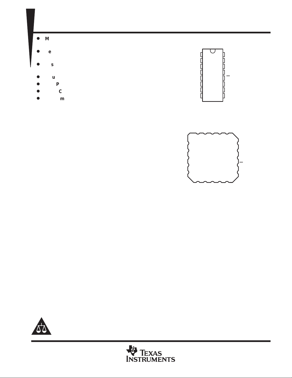
J OR W PACKAGE
(TOP VIEW)
1
2
3
4
5
6
7
8
GND
NC
16
15
14
13
12
11
10
9
CC
V
3B
1B
1A
1Y
G
2Y
2A
2B
GND
FK PACKAGE
(TOP VIEW)
1A1BNC
1Y
4
G
5
NC
6
2Y
7
2A
8
2B
NC – No internal connection
V
CC
4B
4A
4Y
G
3Y
3A
3B
4B
1920132
4A
18
4Y
17
NC
16
G
15
3Y
14
1312119 10
3A
This device offers optimum performance when used with the SN55LBC172M quadruple line driver. The
SN55LBC173 is available in the 16-pin CDIP (J), the 16-pin CPAK (W), or the 20-pin LCCC (FK) packages.
The SN55LBC173 is characterized over the military temperature range of –55°C to 125°C.
Please be aware that an important notice concerning availability, standard warranty, and use in critical applications of
Texas Instruments semiconductor products and disclaimers thereto appears at the end of this data sheet.
LinBiCMOS is a trademark of Texas Instruments Incorporated.
PRODUCTION DATA information is current as of publication date.
Products conform to specifications per the terms of Texas Instruments
standard warranty. Production processing does not necessarily include
testing of all parameters.
POST OFFICE BOX 655303 • DALLAS, TEXAS 75265
Copyright 1995, Texas Instruments Incorporated
1
SN55LBC173
QUADRUPLE LOW-POWER DIFFERENTIAL RECEIVER
SGLS081 – MARCH 1995
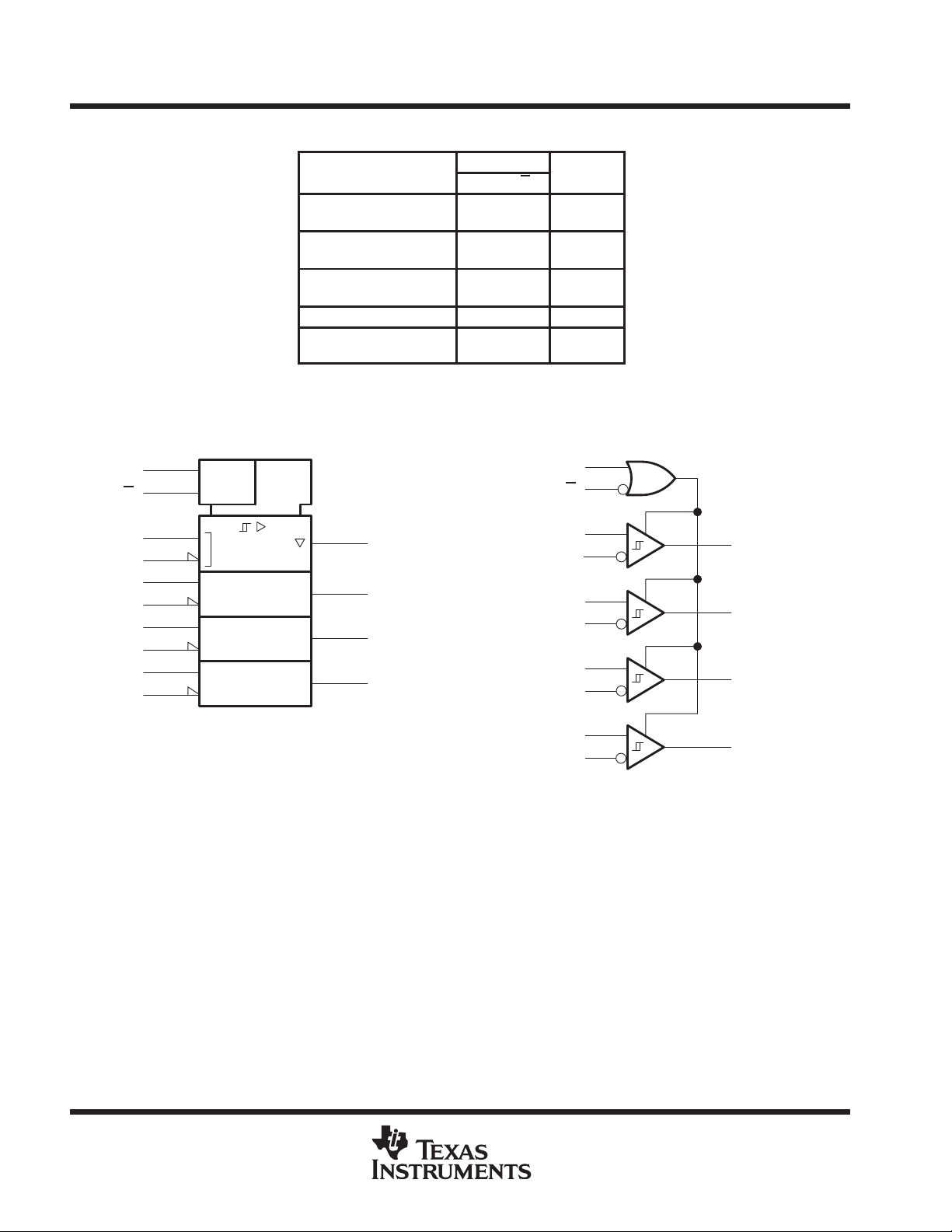
FUNCTION TABLE
(each receiver)
DIFFERENTIAL INPUTS
A–B
VID ≥ 0.2 V
–0.2 V < VID < 0.2 V
VID ≤ –0.2 V
X L H Z
Open circuit
H = high level, L = low level, X = irrelevant,
Z = high impedance (off), ? = indeterminate
ENABLES
G G
H
X
H
X
H
X
H
X
X
L
X
L
X
L
X
L
OUTPUT
Y
H
H
?
?
L
L
H
H
4
12
2
1
6
7
10
9
14
15
†
≥ 1
3
5
11
13
logic symbol
G
G
1A
1B
2A
2B
3A
3B
4A
4B
†
This symbol is in accordance with ANSI/IEEE Std 91-1984
and IEC Publication 617-12.
Pin numbers shown are for the J or W package.
1Y
2Y
3Y
4Y
logic diagram (positive logic)
4
G
12
G
2
1A
1
1B
6
2A
7
2B
10
3A
9
3B
14
4A
15
4B
13
3
1Y
5
2Y
11
3Y
4Y
2
POST OFFICE BOX 655303 • DALLAS, TEXAS 75265
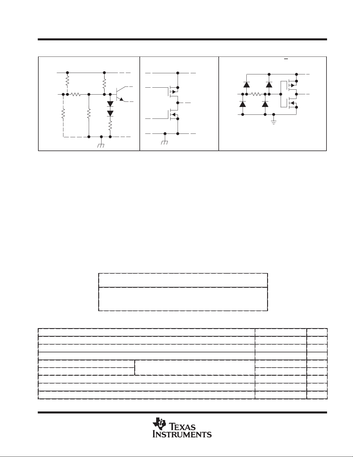
schematics of inputs and outputs
G inputs
SN55LBC173
QUADRUPLE LOW-POWER DIFFERENTIAL RECEIVER
SGLS081 – MARCH 1995
EQUIVALENT OF A AND B INPUTS
V
CC
100 kΩ
A Only
Input
18 kΩ
100 kΩ
B Only
3 kΩ
12 kΩ
Receiver
1 kΩ
TYPICAL OF ALL OUTPUTS
V
CC
Y Output
TYPICAL OF G AND G INPUTS
Input
V
CC
absolute maximum ratings over operating free-air temperature range (unless otherwise noted)
Supply voltage range, V
Input voltage, V
(A or B inputs) ±25 V. . . . . . . . . . . . . . . . . . . . . . . . . . . . . . . . . . . . . . . . . . . . . . . . . . . . . . . . . . . . .
I
Differential input voltage, V
Data and control voltage range –0.3 V to 7 V. . . . . . . . . . . . . . . . . . . . . . . . . . . . . . . . . . . . . . . . . . . . . . . . . . . . . .
Continuous total dissipation See Dissipation Rating Table. . . . . . . . . . . . . . . . . . . . . . . . . . . . . . . . . . . . . . . . . . .
Operating free-air temperature range, T
Storage temperature range, T
Lead temperature 1,6 mm (1/16 inch) from case for 10 seconds 260°C. . . . . . . . . . . . . . . . . . . . . . . . . . . . . . .
†
Stresses beyond those listed under “absolute maximum ratings” may cause permanent damage to the device. These are stress ratings only, and
functional operation of the device at these or any other conditions beyond those indicated under “recommended operating conditions” is not
implied. Exposure to absolute-maximum-rated conditions for extended periods may affect device reliability.
NOTES: 1. All voltage values are with respect to GND.
2. Differential input voltage is measured at the noninverting input with respect to the corresponding inverting input.
(see Note 1) –0.3 V to 7 V. . . . . . . . . . . . . . . . . . . . . . . . . . . . . . . . . . . . . . . . . . . . . .
CC
(see Note 2) ±25 V. . . . . . . . . . . . . . . . . . . . . . . . . . . . . . . . . . . . . . . . . . . . . . . . . . .
ID
–55°C to 125°C. . . . . . . . . . . . . . . . . . . . . . . . . . . . . . . . . . . . . . . . . . .
–65°C to 150°C. . . . . . . . . . . . . . . . . . . . . . . . . . . . . . . . . . . . . . . . . . . . . . . . . . .
stg
A
†
PACKAGE
FK 1375 mW 11.0 mW/°C 275 mW
J 1375 mW 11.0 mW/°C 275 mW
W 1000 mW 8.0 mW/°C 200 mW
POWER RATING
recommended operating conditions
Supply voltage, V
Common-mode input voltage, V
Differential input voltage, V
High-level input voltage, V
Low-level input voltage, V
High-level output current, I
Low-level output current, I
Operating free-air temperature, T
CC
IC
ID
IH
IL
OH
OL
A
DISSIPATION RATING TABLE
TA ≤ 25°C
p
DERATING FACTOR
ABOVE TA = 25°C
TA = 125°C
POWER RATING
MIN NOM MAX UNIT
4.75 5 5.25 V
–7 12 V
±6 V
2 V
0.8 V
–8 mA
16 mA
–55 125 °C
POST OFFICE BOX 655303 • DALLAS, TEXAS 75265
3

SN55LBC173
VOLLow-level output voltage
V
IIBus input current
mA
ICCSupply current
mA
t
Propagation delay time, high-to-low-level output
ID
,
ns
t
Propagation delay time, low-to-high-level output
ID
,
ns
t
Output enable time to high level
See Figure 2
ns
t
Output enable time to low level
See Figure 3
ns
t
Output disable time from high level
See Figure 2
ns
t
Output disable time from low level
See Figure 3
ns
t
)
Pulse skew (|t
PHL
t
PLH
|)
See Figure 1
ns
ttTransition time
See Figure 1
ns
QUADRUPLE LOW-POWER DIFFERENTIAL RECEIVER
SGLS081 – MARCH 1995
electrical characteristics over recommended ranges of supply voltage and operating free-air
temperature (unless otherwise noted)
PARAMETER TEST CONDITIONS MIN TYP†MAX UNIT
V
Positive-going input threshold voltage IO = –8 mA 0.2 V
IT+
V
Negative-going input threshold voltage IO =16 mA –0.2 V
IT–
V
Hysteresis voltage (V
hys
V
Enable input clamp voltage II = –18 mA –0.9 –1.5 V
IK
V
High-level output voltage VID = 200 mV, IOH = –8 mA 3.5 4.5 V
OH
p
I
High-impedance-state output current VO = 0 V to V
OZ
p
I
High-level input current VIH = 5 V ±20 µA
IH
I
Low-level input current VIL = 0 V –20 µA
IL
Short-circuit output
I
OS
current
pp
†
All typical values are at VCC = 5 V and TA = 25°C.
IT+
– V
) 45 mV
IT–
VID = –200 mV, IOL = 16 mA 0.3 0.5
VID = –200 mV, IOL = 16 mA, TA = 125°C 0.7
CC
VIH = 12 V, VCC = 5 V, Other inputs at 0 V 0.7 1
A or B
inputs
VIH = 12 V, VCC = 0 V , Other inputs at 0 V 0.8 1
VIH = –7 V, VCC = 5 V, Other inputs at 0 V –0.5 –0.8
VIH = –7 V, VCC = 0 V, Other inputs at 0 V –0.4 –0.8
VO = 0 –80 –120 mA
Outputs enabled, IO = 0, VID = 5 V 11 20
Outputs disabled 0.9 1.4
±20 µA
switching characteristics, VCC = 5 V, CL = 15 pF
PARAMETER TEST CONDITIONS T
V
PHL
PLH
PZH
PZL
PHZ
PLZ
sk(p
p
p
p
p
p
p
–
p
p
= –1.5 V to 1.5 V,
See Figure 1
V
= –1.5 V to 1.5 V,
See Figure 1
A
25°C 11 22 30
–55°C to 125°C 11 35
25°C 11 22 35
–55°C to 125°C 11 35
25°C 17 40
–55°C to 125°C 45
25°C 18 30
–55°C to 125°C 35
25°C 30 40
–55°C to 125°C 55
25°C 25 40
–55°C to 125°C 45
25°C 0.5 6
–55°C to 125°C 7
25°C 5 10
–55°C to 125°C 16
MIN TYP MAX UNIT
4
POST OFFICE BOX 655303 • DALLAS, TEXAS 75265

QUADRUPLE LOW-POWER DIFFERENTIAL RECEIVER
PARAMETER MEASUREMENT INFORMATION
SN55LBC173
SGLS081 – MARCH 1995
t
PHL
t
t
1.5 V
– 1.5 V
V
OH
V
OL
Generator
(see Note A)
NOTES: A. The input pulse is supplied by a generator having the following characteristics: PRR = 1 MHz, duty cycle ≤ 50%, tr ≤ 6 ns,
tf ≤ 6 ns, ZO = 50 Ω.
B. CL includes probe and jig capacitance.
50 Ω
2 V
Output
CL = 15 pF
(see Note B)
TEST CIRCUIT
Input
Output
t
PLH
90%
10%
t
t
VOLTAGE WAVEFORMS
0 V0 V
1.3 V1.3 V
Figure 1. tpd and tt Test Circuit and Voltage Waveforms
V
CC
1.5 V
Output
CL = 15 pF
(see Note B)
5 kΩ
S1
See Note C
2 kΩ
Input
t
PZH
3 V
1.3 V1.3 V
0 V
t
PHZ
0.5 V
Output
Generator
(see Note A)
NOTES: A. The input pulse is supplied by a generator having the following characteristics: PRR = 1 MHz, duty cycle ≤ 50%, tr ≤ 6 ns,
B. CL includes probe and jig capacitance.
C. All diodes are 1N916 or equivalent.
D. To test the active-low enable G
2 V
50 Ω
(see Note D)
tf ≤ 6 ns, ZO = 50 Ω.
Figure 2. t
TEST CIRCUIT
, ground G and apply an inverted input waveform to G.
and t
PHZ
Test Circuit and Voltage Waveforms
PZH
S1 Open
1.3 V
0 V
VOLTAGE WAVEFORMS
V
S1 Closed
≈ 1.4 V
OH
POST OFFICE BOX 655303 • DALLAS, TEXAS 75265
5

SN55LBC173
QUADRUPLE LOW-POWER DIFFERENTIAL RECEIVER
SGLS081 – MARCH 1995
PARAMETER MEASUREMENT INFORMATION
V
CC
Output
–1.5 V
CL = 15 pF
(see Note B)
5 kΩ
Generator
(see Note A)
NOTES: A. The input pulse is supplied by a generator having the following characteristics: PRR = 1 MHz, duty cycle ≤ 50%, tr ≤ 6 ns,
B. CL includes probe and jig capacitance.
C. All diodes are 1N916 or equivalent.
D. To test the active-low enable G
2 V
S2
50 Ω
(see Note D)
TEST CIRCUIT
tf ≤ 6 ns, ZO = 50 Ω.
, ground G and apply an inverted input waveform to G.
2 kΩ
See Note C
Input
S2 Open
Output
t
PZL
1.3 V 1.3 V
1.3 V
VOLTAGE WAVEFORMS
t
PLZ
S2 Closed
0.5 V
3 V
0 V
≈ 1.4 V
V
OL
DIFFERENTIAL INPUT VOLTAGE
4.5
VCC = 5 V
4
TA = 25°C
3.5
3
2.5
= 0 V
= – 7 V
2
– Output Voltage – V
1.5
O
V
1
0.5
0
01020304050
IC
IC
V
V
VID – Differential Input Voltage – mV
Figure 3. t
PZL
OUTPUT VOLTAGE
vs
= 12 V
= – 7 V
IC
V
IC
V
60 70 80
and t
Test Circuit and Voltage Waveforms
PLZ
TYPICAL CHARACTERISTICS
5.5
5
4.5
4
3.5
3
= 0 V
V
IC
= 12 V
IC
V
90 100
2.5
2
1.5
– High-Level Output Voltage – V
1
OH
V
VID = 0.2 V
0.5
TA = 25°C
0
0 – 4 – 8 – 12 – 16 – 20
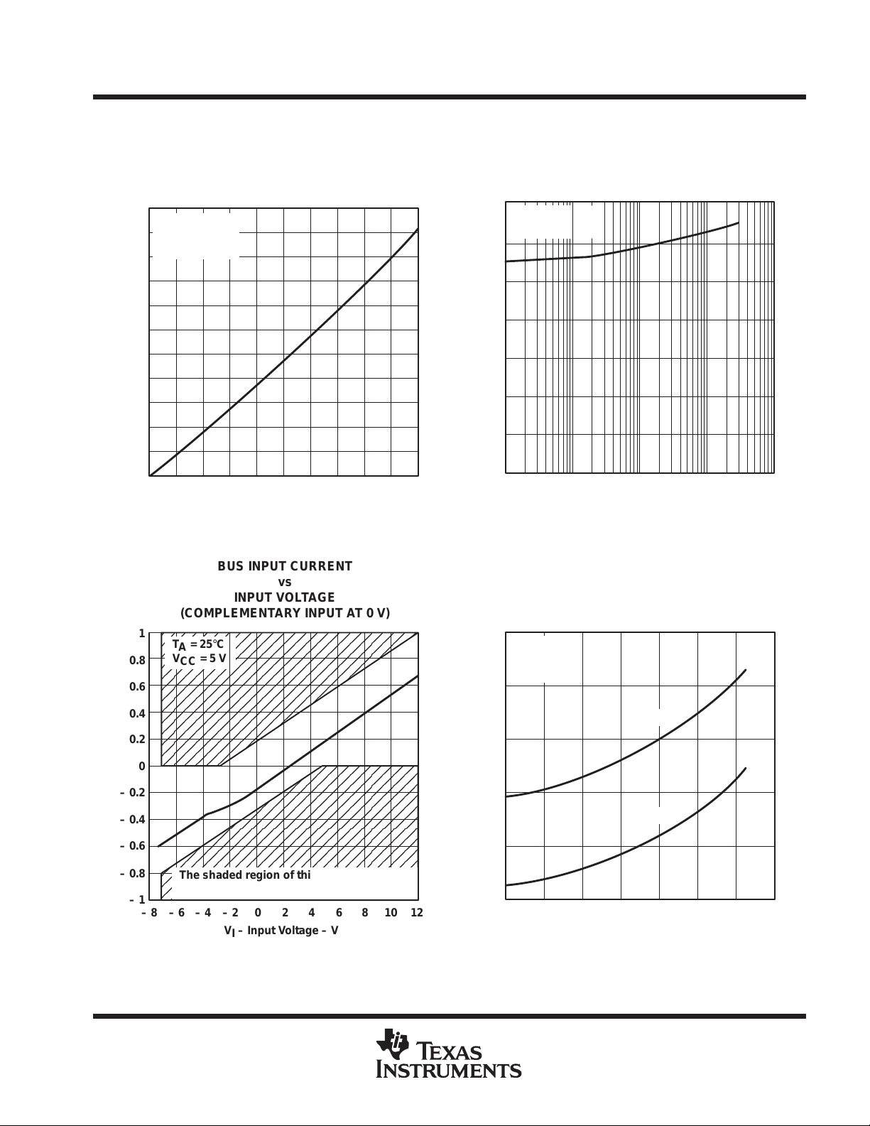
HIGH-LEVEL OUTPUT VOLTAGE
vs
HIGH-LEVEL OUTPUT CURRENT
VCC = 5.25 V
VCC = 5 V
VCC = 4.75 V
– 24 – 28 – 32
IOH – High-Level Output Current – mA
– 36 – 40
Figure 4
6
POST OFFICE BOX 655303 • DALLAS, TEXAS 75265
Figure 5
QUADRUPLE LOW-POWER DIFFERENTIAL RECEIVER
TYPICAL CHARACTERISTICS
SN55LBC173
SGLS081 – MARCH 1995
LOW-LEVEL OUTPUT VOLTAGE
LOW-LEVEL OUTPUT CURRENT
660
TA = 25°C
600
VCC = 5 V
VID = 200 mV
540
480
420
360
300
240
180
– Low-Level Output Voltage – mV
120
OL
V
60
0
03691215
IOL – Low-Level Output Current – mA
BUS INPUT CURRENT
(COMPLEMENTARY INPUT AT 0 V)
1
TA = 25°C
VCC = 5 V
0.8
0.6
vs
18 21 24
Figure 6
vs
INPUT VOLTAGE
27 30
AVERAGE SUPPLY CURRENT
FREQUENCY
14
TA = 25°C
VCC = 5 V
12
10
8
6
4
– Average Supply Current – mA
CC
I
2
0
10 K 100 K 2 M
f – Frequency – Hz
Figure 7
PROPAGATION DELAY TIME
FREE-AIR TEMPERATURE
24.5
VCC = 5 V
CL = 15 pF
VIO = ±1.5 V
24
vs
10 M 100 M
vs
0.4
0.2
0
– 0.2
– 0.4
– Bus Input Current – mAI
I
– 0.6
– 0.8
– 1
The shaded region of this graph represents
more than 1 unit load per RS-485.
– 8– 6– 4– 2 0 2
468
VI – Input Voltage – V
Figure 8
23.5
23
Propagation Delay Time – ns
22.5
22
10 12
POST OFFICE BOX 655303 • DALLAS, TEXAS 75265
– 40 – 20 0 20 40 60
t
PHL
t
PLH
TA – Free-Air Temperature – ° C
Figure 9
80 100
7

IMPORTANT NOTICE
T exas Instruments and its subsidiaries (TI) reserve the right to make changes to their products or to discontinue
any product or service without notice, and advise customers to obtain the latest version of relevant information
to verify, before placing orders, that information being relied on is current and complete. All products are sold
subject to the terms and conditions of sale supplied at the time of order acknowledgement, including those
pertaining to warranty, patent infringement, and limitation of liability.
TI warrants performance of its semiconductor products to the specifications applicable at the time of sale in
accordance with TI’s standard warranty. Testing and other quality control techniques are utilized to the extent
TI deems necessary to support this warranty . Specific testing of all parameters of each device is not necessarily
performed, except those mandated by government requirements.
CERT AIN APPLICATIONS USING SEMICONDUCTOR PRODUCTS MAY INVOLVE POTENTIAL RISKS OF
DEATH, PERSONAL INJURY, OR SEVERE PROPERTY OR ENVIRONMENTAL DAMAGE (“CRITICAL
APPLICATIONS”). TI SEMICONDUCTOR PRODUCTS ARE NOT DESIGNED, AUTHORIZED, OR
WARRANTED TO BE SUITABLE FOR USE IN LIFE-SUPPORT DEVICES OR SYSTEMS OR OTHER
CRITICAL APPLICA TIONS. INCLUSION OF TI PRODUCTS IN SUCH APPLICATIONS IS UNDERST OOD TO
BE FULLY AT THE CUSTOMER’S RISK.
In order to minimize risks associated with the customer’s applications, adequate design and operating
safeguards must be provided by the customer to minimize inherent or procedural hazards.
TI assumes no liability for applications assistance or customer product design. TI does not warrant or represent
that any license, either express or implied, is granted under any patent right, copyright, mask work right, or other
intellectual property right of TI covering or relating to any combination, machine, or process in which such
semiconductor products or services might be or are used. TI’s publication of information regarding any third
party’s products or services does not constitute TI’s approval, warranty or endorsement thereof.
Copyright 1998, Texas Instruments Incorporated
 Loading...