

Texas Instruments SNJ55LBC172FK, SNJ55LBC172J, SNJ55LBC172W Datasheet
SN55LBC172
QUADRUPLE LOW-POWER DIFFERENTIAL LINE DRIVER
SGLS084B – MARCH 1995 – REVISED SEPTEMBER 1999
D
Meets Standard EIA-485
D
Designed for High-Speed Multipoint
Transmission on Long Bus Lines in Noisy
Environments
D
Supports Data Rates up to and Exceeding
Ten Million Transfers Per Second
D
Common-Mode Output Voltage Range of
–7 V to 12 V
D
Positive- and Negative-Current Limiting
D
Low Power Consumption . . . 1.5 mA Max
(Output Disabled)
description
The SN55LBC172 is a monolithic quadruple
differential line driver with 3-state outputs. This
device is designed to meet the requirements of the
Electronics Industry Association (EIA) standard
RS-485. The SN55LBC172 is optimized for
balanced multipoint bus transmission at data
rates up to and exceeding 10 million bits per
second. The driver features wide positive and
negative common-mode output voltage ranges,
current limiting, and thermal-shutdown circuitry,
making it suitable for party-line applications in
noisy environments. The device is designed using
the LinBiCMOS process, facilitating ultralow
power consumption and inherent robustness.
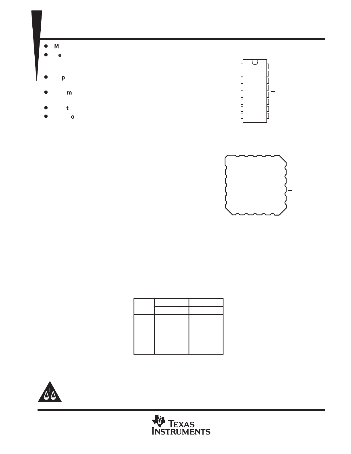
J OR W PACKAGE
(TOP VIEW)
1A
1Y
1Z
G
2Z
2Y
2A
GND
FK PACKAGE
(TOP VIEW)
1Y1ANC
1Z
4
G
5
NC
6
2Z
7
2Y
8
2A
NC – No internal connection
1
2
3
4
5
6
7
8
GND
NC
16
15
14
13
12
11
10
9
CC
V
3A
1920132
1312119 10
V
4A
4Y
4Z
G
3Z
3Y
3A
CC
4A
3Y
18
17
16
15
14
4Y
4Z
NC
G
3Z
The SN55LBC172 provides positive- and negative-current limiting and thermal shutdown for protection from
line fault conditions on the transmission bus line. This device offers optimum performance when used with the
SN55LBC173M quadruple line receiver. The SN55LBC172 is available in the 16-pin CDIP package (J), the
16-pin CPAK package (W), or the 20-pin LCCC package (FK).
The SN55LBC172 is characterized for operation over a military temperature range of –55°C to 125°C.
FUNCTION TABLE
(each driver)
INPUT
A
H H X H L
L H XLH
H X LHL
L X LLH
X L H Z Z
H = high level, L = low level, X = irrelevant,
Z = high impedance (off)
Please be aware that an important notice concerning availability, standard warranty, and use in critical applications of
Texas Instruments semiconductor products and disclaimers thereto appears at the end of this data sheet.
LinBiCMOS is a trademark of Texas Instruments Incorporated.
PRODUCTION DATA information is current as of publication date.
Products conform to specifications per the terms of Texas Instruments
standard warranty. Production processing does not necessarily include
testing of all parameters.
ENABLES OUTPUTS
G
G
Y Z
Copyright 1999, Texas Instruments Incorporated
POST OFFICE BOX 655303 • DALLAS, TEXAS 75265
1
SN55LBC172
QUADRUPLE LOW-POWER DIFFERENTIAL LINE DRIVER
SGLS084B – MARCH 1995 – REVISED SEPTEMBER 1999
4
12
1
7
9
15
†
≥1
EN
2
1Y
3
1Z
6
2Y
5
2Z
10
3Y
11
3Z
14
4Y
13
4Z
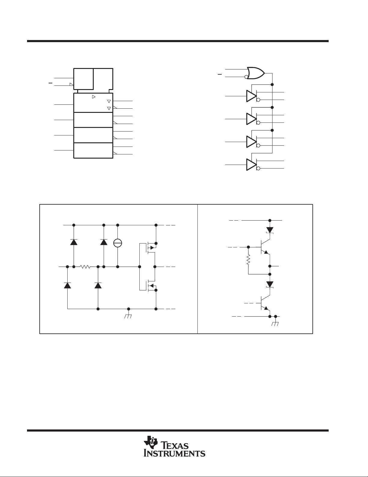
logic symbol
G
G
1A
2A
3A
4A
†
This symbol is in accordance with ANSI/IEEE Std 91-1984
and IEC Publication 617-12.
Pin numbers shown are for the J or W package.
schematic diagrams of inputs and outputs
ALL INPUTS Y OR Z OUTPUT
+
50 µA
–
logic diagram (positive logic)
4
4
G
G
12
12
G
G
1
1
1A
1A
7
7
2A
2A
9
9
3A
3A
15
15
4A
4A
V
V
CC
CC
10
10
11
11
14
14
13
13
2
2
1Y
1Y
3
3
1Z
1Z
6
6
2Y
2Y
5
5
2Z
2Z
3Y
3Y
3Z
3Z
4Y
4Y
4Z
4Z
Input
200 Ω
Output
Driver
2
POST OFFICE BOX 655303 • DALLAS, TEXAS 75265
Output voltage at any bus terminal (separately or common mode), V
Y or Z–7V
SN55LBC172
QUADRUPLE LOW-POWER DIFFERENTIAL LINE DRIVER
SGLS084B – MARCH 1995 – REVISED SEPTEMBER 1999
absolute maximum ratings over operating free-air temperature (unless otherwise noted)
Supply voltage range, V
(see Note 1) –0.3 V to 7 V. . . . . . . . . . . . . . . . . . . . . . . . . . . . . . . . . . . . . . . . . . . . . .
CC
†
Output voltage range, VO –10 V to 15 V. . . . . . . . . . . . . . . . . . . . . . . . . . . . . . . . . . . . . . . . . . . . . . . . . . . . . . . . . . .
Input voltage range, VI –0.3 V to 7 V. . . . . . . . . . . . . . . . . . . . . . . . . . . . . . . . . . . . . . . . . . . . . . . . . . . . . . . . . . . . . .
Continuous power dissipation Internally limited
. . . . . . . . . . . . . . . . . . . . . . . . . . . . . . . . . . . . . . . . . . . . . . . . . . . .
Operating free-air temperature range, TA –55°C to 125°C. . . . . . . . . . . . . . . . . . . . . . . . . . . . . . . . . . . . . . . . . . .
Storage temperature range, T
–65°C to 150°C. . . . . . . . . . . . . . . . . . . . . . . . . . . . . . . . . . . . . . . . . . . . . . . . . . .
stg
Lead temperature 1,6 mm (1/16 inch) from case for 10 seconds –65°C to 150°C. . . . . . . . . . . . . . . . . . . . . . .
†
Stresses beyond those listed under “absolute maximum ratings” may cause permanent damage to the device. These are stress ratings only, and
functional operation of the device at these or any other conditions beyond those indicated under “recommended operating conditions” is not
implied. Exposure to absolute-maximum-rated conditions for extended periods may affect device reliability.
‡
The maximum operating junction temperature is internally limited. Use the dissipation rating table to operate below this temperature.
NOTE 1: All voltage values are with respect to GND.
DISSIPATION RATING TABLE
PACKAGE
FK 1375 mW 11.0 mW/°C 275 mW
J 1375 mW 11.0 mW/°C 275 mW
W 1000 mW 8.0 mW/°C 200 mW
TA ≤ 25°C
POWER RATING
DERATING FACTOR
ABOVE TA=125°C
TA = 125°C
POWER RATING
recommended operating conditions
MIN NOM MAX UNIT
Supply voltage, V
High-level input voltage, V
Low-level input voltage, V
p
CC
IH
IL
p
O
4.75 5 5.25 V
2 V
0.8 V
12
‡
High-level output current, I
Low-level output current, I
Continuous total power dissipation See Dissipation Rating Table
Operating free-air temperature, T
OH
OL
A
Y or Z –60 mA
Y or Z 60 mA
–55 125 °C
POST OFFICE BOX 655303 • DALLAS, TEXAS 75265
3
SN55LBC172
|VOD|
Diff
‡
V
V
C
R
54 Ω
See Figure 1
V
ICCSupply current (all drivers)
No load
mA
t
Differential output delay time
R
See Figure 3
ns
t
Differential output transition time
R
See Figure 3
ns
t
Output enable time to high level
R
110 Ω
See Figure 4
ns
t
Output enable time to low level
R
110 Ω
See Figure 5
ns
t
Output disable time from high level
R
110 Ω
See Figure 4
ns
t
PLZ
Out ut disable time from low level
R
L
110 Ω
See Figure 5
ns
QUADRUPLE LOW-POWER DIFFERENTIAL LINE DRIVER
SGLS084B – MARCH 1995 – REVISED SEPTEMBER 1999
electrical characteristics over recommended ranges of supply voltage and operating free-air
temperature (unless otherwise noted)
PARAMETER TEST CONDITIONS MIN TYP†MAX UNIT
V
IK
∆|VOD|
OC
∆|VOC|
I
O
I
OZ
I
IH
I
IL
I
OS
†
All typical values are at VCC = 5 V and TA = 25°C.
‡
The minimum VOD specification does not fully comply with EIA-485 at operating temperatures below 0°C. The lower output signal should be used
to determine the maximum signal transmission distance.
§
∆|VOD| and ∆|VOC| are the changes in magnitude of VOD and VOC, respectively, that occur when the input is changed from a high level to a low
level.
Input clamp voltage II = –18 mA –1.5 V
erential output voltage
Change in magnitude of differential output voltage
ommon-mode output voltage
Change in magnitude of common-mode output voltage
Output current with power off VCC = 0, VO = – 7 V to 12 V ±100 µA
High-impedance-state output current VO = – 7 V to 12 V ±100 µA
High-level input current VI = 2.4 V –100 µA
Low-level input current VI = 0.4 V –100 µA
Short-circuit output current VO = –7 V to 12 V ±250 mA
pp
§
RL = 54 Ω, See Figure 1 1.1 1.8 5
RL = 60 Ω, See Figure 2 1.1 1.7 5
,
=
L
§
Outputs enabled 7
Outputs disabled 1.5
±0.2 V
3
–1
±0.2 V
switching characteristics, VCC = 5 V
PARAMETER TEST CONDITIONS T
d(OD)
t(OD)
PZH
PZL
PHZ
p
p
p
p
p
p
= 54 Ω,
L
= 54 Ω,
L
=
L
=
L
=
L
=
A
25°C 2 11 20
–55°C to 125°C 2 40
25°C 10 15 25
–55°C to 125°C 4 60
,
,
,
,
25°C 30
–55°C to 125°C 40
25°C 30
–55°C to 125°C 40
25°C 60
–55°C to 125°C 115
25°C 30
–55°C to 125°C 55
MIN TYP MAX UNIT
4
POST OFFICE BOX 655303 • DALLAS, TEXAS 75265
 Loading...