

Texas Instruments SN74LVC32AD, SN74LVC32ADB, SN74LVC32ANS, SN74LVC32APW, SN74LVC32ARGY Schematic [ru]
...
www.ti.com
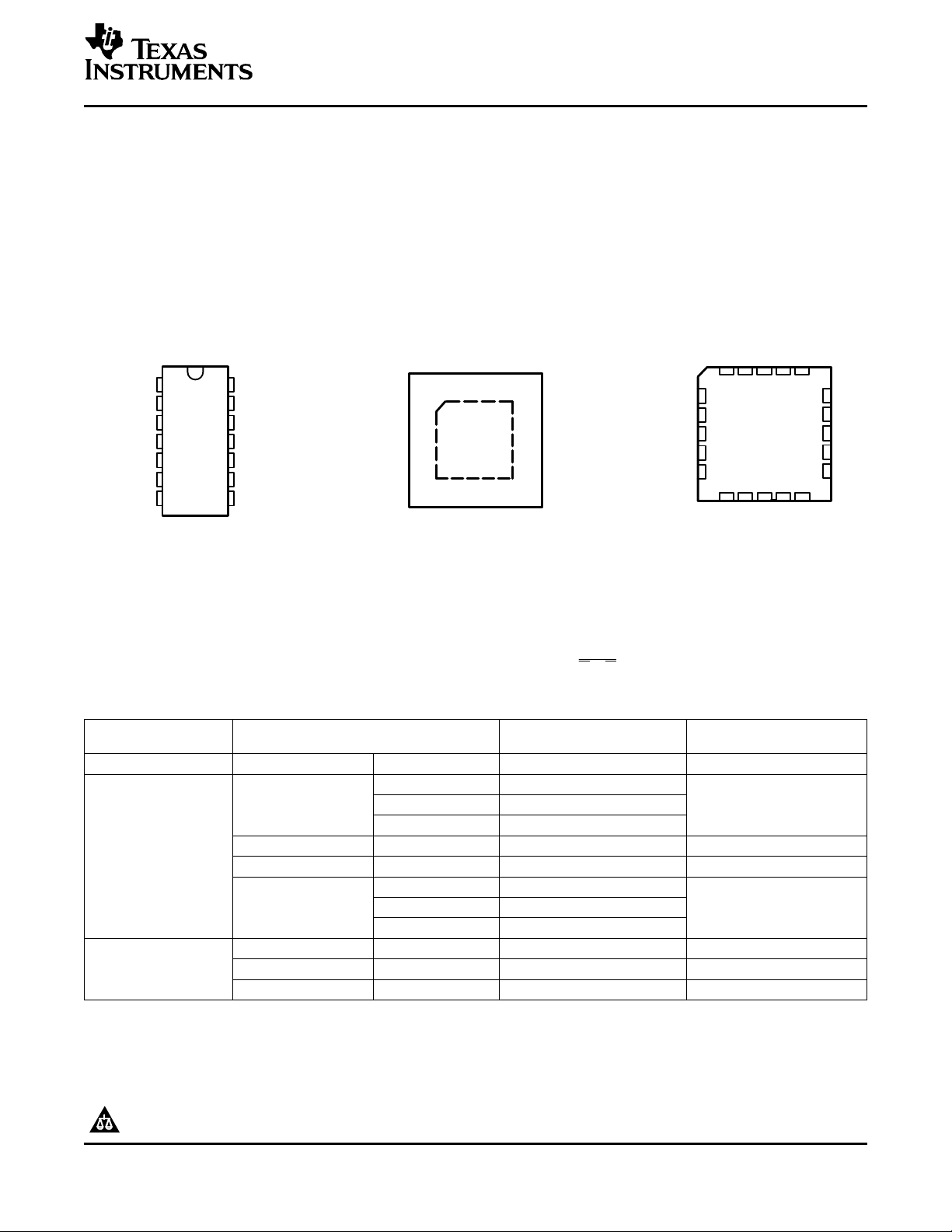
SN74LVC32A . . . RGY PACKAGE
(TOP VIEW)
1 14
7 8
2
3
4
5
6
13
12
11
10
9
4B
4A
4Y
3B
3A
1B
1Y
2A
2B
2Y
1A
3Y
V
GND
CC
1
2
3
4
5
6
7
14
13
12
11
10
9
8
1A
1B
1Y
2A
2B
2Y
GND
V
CC
4B
4A
4Y
3B
3A
3Y
SN54LVC32A . . . J OR W PACKAGE
SN74LVC32A . . . D, DB, NS,
OR PW PACKAGE
(TOP VIEW)
3 2 1 20 19
9 10 11 12 13
4
5
6
7
8
18
17
16
15
14
4A
NC
4Y
NC
3B
1Y
NC
2A
NC
2B
1B1ANC
3Y
3A
V
4B
2Y
GND
NC
SN54LVC32A . . . FK PACKAGE
(TOP VIEW)
CC
NC - No internal connection
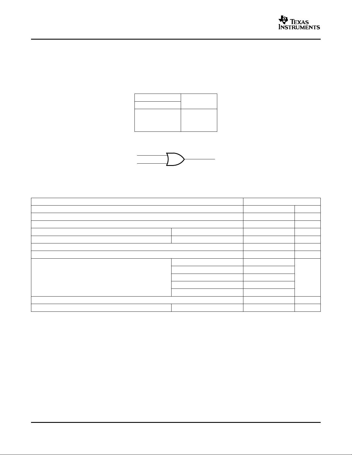
Y A B or Y A • B
SN54LVC32A, SN74LVC32A
QUADRUPLE 2-INPUT POSITIVE-OR GATES
SCAS286P – JANUARY 1993 – REVISED APRIL 2005
FEATURES
• Operate From 1.65 V to 3.6 V
• Specified From –40°C to 85°C,
–40°C to 125°C, and –55°C to 125°C
• Inputs Accept Voltages to 5.5 V
• Max tpdof 3.8 ns at 3.3 V
• Typical V
<0.8 V at V
OLP
CC
(Output Ground Bounce)
= 3.3 V, T
= 25°C – 1000-V Charged-Device Model (C101)
A
• Typical V
>2 V at V
OHV
CC
(Output V
= 3.3 V, T
A
OH
= 25°C
Undershoot)
• Latch-Up Performance Exceeds 250 mA Per
JESD 17
• ESD Protection Exceeds JESD 22
– 2000-V Human-Body Model (A114-A)
– 200-V Machine Model (A115-A)
DESCRIPTION/ORDERING INFORMATION
The SN54LVC32A quadruple 2-input positive-OR gate is designed for 2.7-V to 3.6-V V
SN74LVC32A quadruple 2-input positive-OR gate is designed for 1.65-V to 3.6-V V
The 'LVC32A devices perform the Boolean function
T
A
–40°C to 85°C QFN – RGY Reel of 1000 SN74LVC32ARGYR LC32A
–40°C to 125°C
–55°C to 125°C CFP – W Tube of 150 SNJ54LVC32AW SNJ54LVC32AW
(1) Package drawings, standard packing quantities, thermal data, symbolization, and PCB design guidelines are available at
www.ti.com/sc/package.
PRODUCTION DATA information is current as of publication date.
Products conform to specifications per the terms of the Texas
Instruments standard warranty. Production processing does not
necessarily include testing of all parameters.
Please be aware that an important notice concerning availability, standard warranty, and use in critical applications of Texas
Instruments semiconductor products and disclaimers thereto appears at the end of this data sheet.
in positive logic.
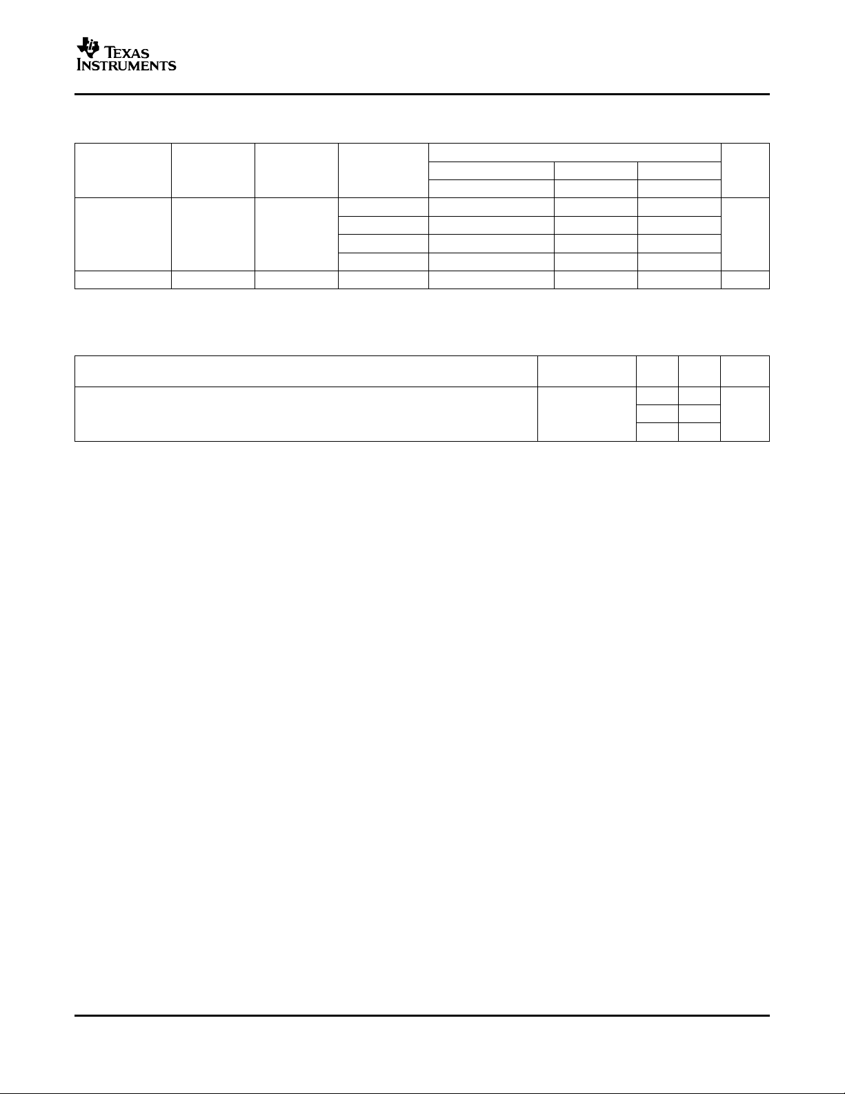
ORDERING INFORMATION
PACKAGE
SOIC – D Reel of 2500 SN74LVC32ADR LVC32A
SOP – NS Reel of 2000 SN74LVC32ANSR LVC32A
SSOP – DB Reel of 2000 SN74LVC32ADBR LC32A
TSSOP – PW Reel of 2000 SN74LVC32APWR LC32A
CDIP – J Tube of 25 SNJ54LVC32AJ SNJ54LVC32AJ
LCCC – FK Tube of 55 SNJ54LVC32AFK SNJ54LVC32AFK
(1)
Tube of 50 SN74LVC32AD
Reel of 250 SN74LVC32ADT
Tube of 90 SN74LVC32APW
Reel of 250 SN74LVC32APWT
ORDERABLE TOP-SIDE
PART NUMBER MARKING
Copyright © 1993–2005, Texas Instruments Incorporated
On products compliant to MIL-PRF-38535, all parameters are
tested unless otherwise noted. On all other products, production
processing does not necessarily include testing of all parameters.
CC
operation.
CC
operation, and the
www.ti.com
A
B
Y
SN54LVC32A, SN74LVC32A
QUADRUPLE 2-INPUT POSITIVE-OR GATES
SCAS286P – JANUARY 1993 – REVISED APRIL 2005
DESCRIPTION/ORDERING INFORMATION (CONTINUED)
Inputs can be driven from either 3.3-V or 5-V devices. This feature allows the use of these devices as translators
in a mixed 3.3-V/5-V system environment.
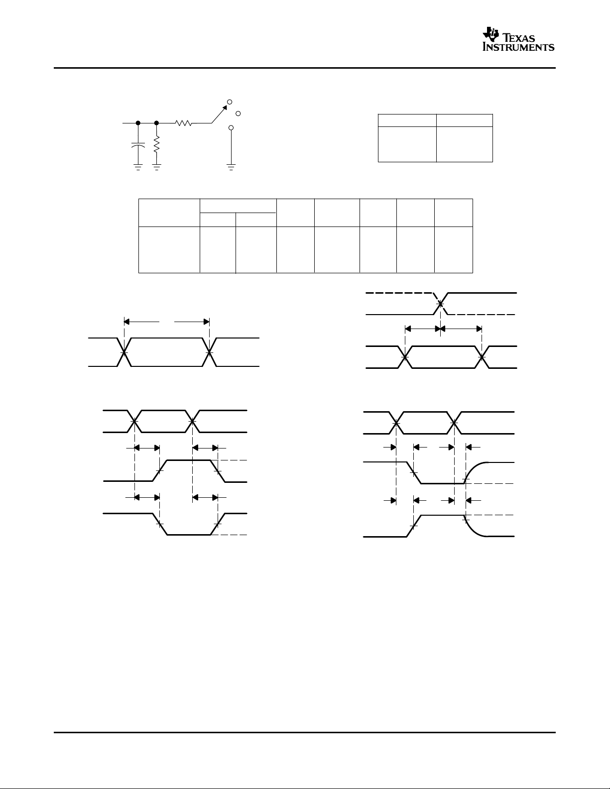
FUNCTION TABLE
(EACH GATE)
INPUTS
A B
H X H
X H H
L L L
LOGIC DIAGRAM, EACH GATE (POSITIVE LOGIC)
OUTPUT
Y
Absolute Maximum Ratings
(1)
over operating free-air temperature range (unless otherwise noted)
MIN MAX UNIT
V
CC
V
I
V
O
I
IK
I
OK
I
O
θ
JA
T
stg
P
tot
(1) Stresses beyond those listed under "absolute maximum ratings" may cause permanent damage to the device. These are stress ratings
(2) The input negative-voltage and output voltage ratings may be exceeded if the input and output current ratings are observed.
(3) The value of V
(4) The package thermal impedance is calculated in accordance with JESD 51-7.
(5) The package thermal impedance is calculated in accordance with JESD 51-5.
(6) For the D package: above 70°C, the value of P
(7) For the DB, DGV, NS, and PW packages: above 60°C, the value of P
Supply voltage range –0.5 6.5 V
Input voltage range
Output voltage range
(2)
(2) (3)
–0.5 6.5 V
–0.5 V
Input clamp current VI< 0 –50 mA
Output clamp current VO< 0 –50 mA
Continuous output current ±50 mA
Continuous current through V
Package thermal impedance NS package
or GND ±100 mA
CC
D package
DB package
PW package
RGY package
(4)
(4)
(4)
(4)
(5)
Storage temperature range –65 150 °C
Power dissipation TA= –40°C to 125°C
(6) (7)
only, and functional operation of the device at these or any other conditions beyond those indicated under "recommended operating
conditions" is not implied. Exposure to absolute-maximum-rated conditions for extended periods may affect device reliability.
is provided in the recommended operating conditions table.
CC
derates linearly with 8 mW/K.
tot
derates linearly with 5.5 mW/K.
tot
+ 0.5 V
CC
86
96
76 °C/W
113
47
500 mW
2
www.ti.com
SN54LVC32A, SN74LVC32A
QUADRUPLE 2-INPUT POSITIVE-OR GATES
SCAS286P – JANUARY 1993 – REVISED APRIL 2005
Recommended Operating Conditions
V
V
V
V
V
I
OH
I
OL
∆ t/ ∆ v Input transition rise or fall rate 7 ns/V
(1) All unused inputs of the device must be held at V
Supply voltage V
CC
High-level input voltage V
IH
Low-level input voltage V
IL
Input voltage 0 5.5 V
I
Output voltage 0 V
O
High-level output current mA
Low-level output current mA
Implications of Slow or Floating CMOS Inputs, literature number SCBA004.
(1)
Operating 2 3.6
Data retention only 1.5
= 2.7 V to 3.6 V 2 V
CC
= 2.7 V to 3.6 V 0.8 V
CC
V
= 2.7 V –12
CC
V
= 3 V –24
CC
V
= 2.7 V 12
CC
V
= 3 V 24
CC
or GND to ensure proper device operation. Refer to the TI application report,
CC
SN54LVC32A
–55 TO 125°C UNIT
MIN MAX
V
CC
Recommended Operating Conditions
(1)
SN74LVC32A
TA= 25° C –40 TO 85° C –40 TO 125° C UNIT
MIN MAX MIN MAX MIN MAX
V
V
V
V
V
I
I
Supply voltage V
CC
High-level input
IH
voltage
Low-level input
IL
voltage
Input voltage 0 5.5 0 5.5 0 5.5 V
I
Output voltage 0 V
O
High-level output
OH
current
Low-level output
OL
current
Operating 1.65 3.6 1.65 3.6 1.65 3.6
Data retention only 1.5 1.5 1.5
V
= 1.65 V to 1.95 V 0.65 × V
CC
V
= 2.3 V to 2.7 V 1.7 1.7 1.7 V
CC
V
= 2.7 V to 3.6 V 2 2 2
CC
V
= 1.65 V to 1.95 V 0.35 × V
CC
V
= 2.3 V to 2.7 V 0.7 0.7 0.7 V
CC
V
= 2.7 V to 3.6 V 0.8 0.8 0.8
CC
V
= 1.65 V –4 –4 –4
CC
V
= 2.3 V –8 –8 –8
CC
V
= 2.7 V –12 –12 –12
CC
V
= 3 V –24 –24 –24
CC
V
= 1.65 V 4 4 4
CC
V
= 2.3 V 8 8 8
CC
V
= 2.7 V 12 12 12
CC
V
= 3 V 24 24 24
CC
CC
0.65 × V
CC
CC
CC
0.35 × V
0 V
0.65 × V
CC
CC
CC
0.35 × V
0 V
∆ t/ ∆ v Input transition rise or fall rate 7 7 7 ns/V
(1) All unused inputs of the device must be held at V
Implications of Slow or Floating CMOS Inputs, literature number SCBA004.
or GND to ensure proper device operation. Refer to the TI application report,
CC
CC
V
CC
mA
mA
3
www.ti.com
SN54LVC32A, SN74LVC32A
QUADRUPLE 2-INPUT POSITIVE-OR GATES
SCAS286P – JANUARY 1993 – REVISED APRIL 2005
Electrical Characteristics
over operating free-air temperature range (unless otherwise noted)
PARAMETER TEST CONDITIONS V
IOH= –100 µ A 2.7 V to 3.6 V V
V
OH
V
OL
I
I
I
CC
∆ I
CC
Electrical Characteristics
over operating free-air temperature range (unless otherwise noted)
PARAMETER TEST CONDITIONS V
V
OH
V
OL
I
I
I
CC
∆ I
CC
C
i
IOH= –12 mA V
IOH= –24 mA 3 V 2.2
IOL= 100 µ A 2.7 V to 3.6 V 0.2
IOL= 12 mA 2.7 V 0.4 V
IOL= 24 mA 3 V 0.55
VI= 5.5 V or GND 3.6 V ±5 µ A
VI= V
One input at V
or GND, IO= 0 3.6 V 10 µ A
CC
– 0.6 V, Other inputs at V
CC
or GND 2.7 V to 3.6 V 500 µ A
CC
SN74LVC32A
CC
TA= 25°C –40 TO 85°C –40 TO 125°C UNIT
MIN TYP MAX MIN MAX MIN MAX
IOH= –100 µ A 1.65 V to 3.6 V V
– 0.2 V
CC
IOH= –4 mA 1.65 V 1.29 1.2 1.05
IOH= –8 mA 2.3 V 1.9 1.7 1.55
IOH= –12 mA
2.7 V 2.2 2.2 2.05
3 V 2.4 2.4 2.25
IOH= –24 mA 3 V 2.3 2.2 2
IOL= 100 µ A 1.65 V to 3.6 V 0.1 0.2 0.3
IOL= 4 mA 1.65 V 0.24 0.45 0.6
IOL= 8 mA 2.3 V 0.3 0.7 0.85 V
IOL= 12 mA 2.7 V 0.4 0.4 0.6
IOL= 24 mA 3 V 0.55 0.55 0.8
VI= 5.5 V or GND 3.6 V ±1 ±5 ±20 µ A
VI= V
One input at V
Other inputs at V
GND
VI= V
or GND, IO= 0 3.6 V 1 10 40 µ A
CC
– 0.6 V,
CC
or 2.7 V to 3.6 V 500 500 5000 µ A
CC
or GND 3.3 V 5 pF
CC
CC
2.7 V 2.2
3 V 2.4
– 0.2 V
CC
SN54LVC32A
–55 TO 125°C UNIT
MIN MAX
– 0.2
CC
– 0.3
CC
V
Switching Characteristics
over operating free-air temperature range (unless otherwise noted) (see Figure 1)
PARAMETER V
t
pd
4
FROM TO
(INPUT) (OUTPUT)
A or B Y ns
SN54LVC32A
CC
–55 TO 125°C UNIT
MIN MAX
2.7 V 4.4
3.3 V ± 0.3 V 1 3.8
www.ti.com
QUADRUPLE 2-INPUT POSITIVE-OR GATES
Switching Characteristics
over operating free-air temperature range (unless otherwise noted) (see Figure 1)
PARAMETER V
t
pd
t
sk(o)
Operating Characteristics
TA= 25°C
C
Power dissipation capacitance per gate f = 10 MHz 2.5 V 10.6 pF
pd
FROM TO
(INPUT) (OUTPUT)
A or B Y ns
PARAMETER V
CC
1.8 V ± 0.15 V 1 4.2 8.2 1 8.7 1 10.2
2.5 V ± 0.2 V 1 2.6 4.9 1 5.4 1 6.9
2.7 V 1 3 4.2 1 4.4 1 5.5
3.3 V ± 0.3 V 1 2.5 3.6 1 3.8 1 5
3.3 V ± 0.3 V 1 1.5 ns
TA= 25°C –40 TO 85°C –40 TO 125°C UNIT
MIN TYP MAX MIN MAX MIN MAX
SN54LVC32A, SN74LVC32A
SCAS286P – JANUARY 1993 – REVISED APRIL 2005
SN74LVC32A
TEST
CONDITIONS
1.8 V 7.5
3.3 V 12.5
TYP UNIT
CC
5
www.ti.com
V
M
t
h
t
su
From Output
Under Test
C
L
(see Note A)
LOAD CIRCUIT
S1
V
LOAD
Open
GND
R
L
R
L
Data Input
Timing Input
V
I
0 V
V
I
0 V
0 V
t
w
Input
VOLTAGE WAVEFORMS
SETUP AND HOLD TIMES
VOLTAGE WAVEFORMS
PROPAGATION DELAY TIMES
INVERTING AND NONINVERTING OUTPUTS
VOLTAGE WAVEFORMS
PULSE DURATION
t
PLH
t
PHL
t
PHL
t
PLH
V
OH
V
OH
V
OL
V
OL
V
I
0 V
Input
Output
Waveform 1
S1 at V
LOAD
(see Note B)
Output
Waveform 2
S1 at GND
(see Note B)
V
OL
V
OH
t
PZL
t
PZH
t
PLZ
t
PHZ
V
LOAD
/2
0 V
VOL + V
∆
VOH - V
∆
≈0 V
V
I
VOLTAGE WAVEFORMS
ENABLE AND DISABLE TIMES
LOW- AND HIGH-LEVEL ENABLING
Output
Output
t
PLH/tPHL
t
PLZ/tPZL
t
PHZ/tPZH
Open
V
LOAD
GND
TEST S1
NOTES: A. CL includes probe and jig capacitance.
B. Waveform 1 is for an output with internal conditions such that the output is low, except when disabled by the output control.
Waveform2 is for an output with internal conditions such that the output is high, except when disabled by the output control.
C. All input pulses are supplied by generators having the following characteristics: PRR ≤ 10 MHz, ZO = 50 Ω.
D. The outputs are measured one at a time, with one transition per measurement.
E. t
PLZ
and t
PHZ
are the same as t
dis
.
F. t
PZL
and t
PZH
are the same as ten.
G. t
PLH
and t
PHL
are the same as tpd.
H. All parameters and waveforms are not applicable to all devices.
Output
Control
V
M
V
M
V
M
V
M
V
M
V
M
V
M
V
M
V
M
V
M
V
M
V
M
V
I
V
M
V
M
1.8 V ± 0.15 V
2.5 V ± 0.2 V
2.7 V
3.3 V ± 0.3 V
1 kΩ
500 Ω
500 Ω
500 Ω
V
CC
R
L
2 × V
CC
2 × V
CC
6 V
6 V
V
LOAD
C
L
30 pF
30 pF
50 pF
50 pF
0.15 V
0.15 V
0.3 V
0.3 V
V
∆
V
CC
V
CC
2.7 V
2.7 V
V
I
VCC/2
VCC/2
1.5 V
1.5 V
V
M
tr/t
f
≤2 ns
≤2 ns
≤2.5 ns
≤2.5 ns
INPUTS
SN54LVC32A, SN74LVC32A
QUADRUPLE 2-INPUT POSITIVE-OR GATES
SCAS286P – JANUARY 1993 – REVISED APRIL 2005
PARAMETER MEASUREMENT INFORMATION
6
Figure 1. Load Circuit and Voltage Waveforms
PACKAGE OPTION ADDENDUM
www.ti.com
PACKAGING INFORMATION
Orderable Device Status
5962-9761801Q2A ACTIVE LCCC FK 20 1 TBD POST-PLATE N / A for Pkg Type -55 to 125 5962-
5962-9761801QCA ACTIVE CDIP J 14 1 TBD A42 N / A for Pkg Type -55 to 125 5962-9761801QC
5962-9761801QDA ACTIVE CFP W 14 1 TBD A42 N / A for Pkg Type -55 to 125 5962-9761801QD
SN74LVC32AD ACTIVE SOIC D 14 50 Green (RoHS
SN74LVC32ADBLE OBSOLETE SSOP DB 14 TBD Call TI Call TI -40 to 85
SN74LVC32ADBR ACTIVE SSOP DB 14 2000 Green (RoHS
SN74LVC32ADBRG4 ACTIVE SSOP DB 14 2000 Green (RoHS
SN74LVC32ADE4 ACTIVE SOIC D 14 50 Green (RoHS
SN74LVC32ADG4 ACTIVE SOIC D 14 50 Green (RoHS
SN74LVC32ADR ACTIVE SOIC D 14 2500 Green (RoHS
SN74LVC32ADRE4 ACTIVE SOIC D 14 2500 Green (RoHS
SN74LVC32ADRG4 ACTIVE SOIC D 14 2500 Green (RoHS
SN74LVC32ADT ACTIVE SOIC D 14 250 Green (RoHS
SN74LVC32ADTE4 ACTIVE SOIC D 14 250 Green (RoHS
SN74LVC32ADTG4 ACTIVE SOIC D 14 250 Green (RoHS
SN74LVC32ANSR ACTIVE SO NS 14 2000 Green (RoHS
Package Type Package
(1)
Drawing
Pins Package
Qty
Eco Plan
(2)
& no Sb/Br)
& no Sb/Br)
& no Sb/Br)
& no Sb/Br)
& no Sb/Br)
& no Sb/Br)
& no Sb/Br)
& no Sb/Br)
& no Sb/Br)
& no Sb/Br)
& no Sb/Br)
& no Sb/Br)
Lead/Ball Finish
(6)
MSL Peak Temp
(3)
Op Temp (°C) Device Marking
9761801Q2A
SNJ54LVC
32AFK
A
SNJ54LVC32AJ
A
SNJ54LVC32AW
CU NIPDAU Level-1-260C-UNLIM -40 to 85 LVC32A
CU NIPDAU Level-1-260C-UNLIM -40 to 85 LC32A
CU NIPDAU Level-1-260C-UNLIM -40 to 85 LC32A
CU NIPDAU Level-1-260C-UNLIM -40 to 85 LVC32A
CU NIPDAU Level-1-260C-UNLIM -40 to 85 LVC32A
CU NIPDAU Level-1-260C-UNLIM -40 to 85 LVC32A
CU NIPDAU Level-1-260C-UNLIM -40 to 85 LVC32A
CU NIPDAU Level-1-260C-UNLIM -40 to 85 LVC32A
CU NIPDAU Level-1-260C-UNLIM -40 to 85 LVC32A
CU NIPDAU Level-1-260C-UNLIM -40 to 85 LVC32A
CU NIPDAU Level-1-260C-UNLIM -40 to 85 LVC32A
CU NIPDAU Level-1-260C-UNLIM -40 to 85 LVC32A
18-Oct-2013
Samples
(4/5)
Addendum-Page 1
PACKAGE OPTION ADDENDUM
www.ti.com
Orderable Device Status
SN74LVC32ANSRE4 ACTIVE SO NS 14 2000 Green (RoHS
Package Type Package
(1)
Drawing
Pins Package
Qty
Eco Plan
(2)
Lead/Ball Finish
(6)
MSL Peak Temp
(3)
Op Temp (°C) Device Marking
CU NIPDAU Level-1-260C-UNLIM -40 to 85 LVC32A
& no Sb/Br)
SN74LVC32ANSRG4 ACTIVE SO NS 14 2000 Green (RoHS
CU NIPDAU Level-1-260C-UNLIM -40 to 85 LVC32A
& no Sb/Br)
SN74LVC32APW ACTIVE TSSOP PW 14 90 Green (RoHS
CU NIPDAU Level-1-260C-UNLIM -40 to 85 LC32A
& no Sb/Br)
SN74LVC32APWE4 ACTIVE TSSOP PW 14 90 Green (RoHS
CU NIPDAU Level-1-260C-UNLIM -40 to 85 LC32A
& no Sb/Br)
SN74LVC32APWG4 ACTIVE TSSOP PW 14 90 Green (RoHS
CU NIPDAU Level-1-260C-UNLIM -40 to 85 LC32A
& no Sb/Br)
SN74LVC32APWLE OBSOLETE TSSOP PW 14 TBD Call TI Call TI -40 to 85
SN74LVC32APWR ACTIVE TSSOP PW 14 2000 Green (RoHS
CU NIPDAU | CU SN Level-1-260C-UNLIM -40 to 85 LC32A
& no Sb/Br)
SN74LVC32APWRE4 ACTIVE TSSOP PW 14 2000 Green (RoHS
CU NIPDAU Level-1-260C-UNLIM -40 to 85 LC32A
& no Sb/Br)
SN74LVC32APWRG3 ACTIVE TSSOP PW 14 2000 Green (RoHS
CU SN Level-1-260C-UNLIM -40 to 85 LC32A
& no Sb/Br)
SN74LVC32APWRG4 ACTIVE TSSOP PW 14 2000 Green (RoHS
CU NIPDAU Level-1-260C-UNLIM -40 to 85 LC32A
& no Sb/Br)
SN74LVC32APWT ACTIVE TSSOP PW 14 250 Green (RoHS
CU NIPDAU Level-1-260C-UNLIM -40 to 85 LC32A
& no Sb/Br)
SN74LVC32APWTE4 ACTIVE TSSOP PW 14 250 Green (RoHS
CU NIPDAU Level-1-260C-UNLIM -40 to 85 LC32A
& no Sb/Br)
SN74LVC32APWTG4 ACTIVE TSSOP PW 14 250 Green (RoHS
CU NIPDAU Level-1-260C-UNLIM -40 to 85 LC32A
& no Sb/Br)
SN74LVC32ARGYR ACTIVE VQFN RGY 14 3000 Green (RoHS
CU NIPDAU Level-2-260C-1 YEAR -40 to 85 LC32A
& no Sb/Br)
SN74LVC32ARGYRG4 ACTIVE VQFN RGY 14 3000 Green (RoHS
CU NIPDAU Level-2-260C-1 YEAR -40 to 85 LC32A
& no Sb/Br)
SNJ54LVC32AFK ACTIVE LCCC FK 20 1 TBD POST-PLATE N / A for Pkg Type -55 to 125 5962-
SNJ54LVC32AJ ACTIVE CDIP J 14 1 TBD A42 N / A for Pkg Type -55 to 125 5962-9761801QC
18-Oct-2013
Samples
(4/5)
9761801Q2A
SNJ54LVC
32AFK
A
SNJ54LVC32AJ
Addendum-Page 2

PACKAGE OPTION ADDENDUM
www.ti.com
Orderable Device Status
SNJ54LVC32AW ACTIVE CFP W 14 1 TBD A42 N / A for Pkg Type -55 to 125 5962-9761801QD
(1)
The marketing status values are defined as follows:
ACTIVE: Product device recommended for new designs.
LIFEBUY: TI has announced that the device will be discontinued, and a lifetime-buy period is in effect.
NRND: Not recommended for new designs. Device is in production to support existing customers, but TI does not recommend using this part in a new design.
PREVIEW: Device has been announced but is not in production. Samples may or may not be available.
OBSOLETE: TI has discontinued the production of the device.
Package Type Package
(1)
Drawing
Pins Package
Qty
Eco Plan
(2)
Lead/Ball Finish
(6)
MSL Peak Temp
(3)
Op Temp (°C) Device Marking
A
SNJ54LVC32AW
18-Oct-2013
(4/5)
(2)
Eco Plan - The planned eco-friendly classification: Pb-Free (RoHS), Pb-Free (RoHS Exempt), or Green (RoHS & no Sb/Br) - please check http://www.ti.com/productcontent for the latest availability
information and additional product content details.
TBD: The Pb-Free/Green conversion plan has not been defined.
Pb-Free (RoHS): TI's terms "Lead-Free" or "Pb-Free" mean semiconductor products that are compatible with the current RoHS requirements for all 6 substances, including the requirement that
lead not exceed 0.1% by weight in homogeneous materials. Where designed to be soldered at high temperatures, TI Pb-Free products are suitable for use in specified lead-free processes.
Pb-Free (RoHS Exempt): This component has a RoHS exemption for either 1) lead-based flip-chip solder bumps used between the die and package, or 2) lead-based die adhesive used between
the die and leadframe. The component is otherwise considered Pb-Free (RoHS compatible) as defined above.
Green (RoHS & no Sb/Br): TI defines "Green" to mean Pb-Free (RoHS compatible), and free of Bromine (Br) and Antimony (Sb) based flame retardants (Br or Sb do not exceed 0.1% by weight
in homogeneous material)
(3)
MSL, Peak Temp. - The Moisture Sensitivity Level rating according to the JEDEC industry standard classifications, and peak solder temperature.
(4)
There may be additional marking, which relates to the logo, the lot trace code information, or the environmental category on the device.
(5)
Multiple Device Markings will be inside parentheses. Only one Device Marking contained in parentheses and separated by a "~" will appear on a device. If a line is indented then it is a continuation
of the previous line and the two combined represent the entire Device Marking for that device.
(6)
Lead/Ball Finish - Orderable Devices may have multiple material finish options. Finish options are separated by a vertical ruled line. Lead/Ball Finish values may wrap to two lines if the finish
value exceeds the maximum column width.
Important Information and Disclaimer:The information provided on this page represents TI's knowledge and belief as of the date that it is provided. TI bases its knowledge and belief on information
provided by third parties, and makes no representation or warranty as to the accuracy of such information. Efforts are underway to better integrate information from third parties. TI has taken and
continues to take reasonable steps to provide representative and accurate information but may not have conducted destructive testing or chemical analysis on incoming materials and chemicals.
TI and TI suppliers consider certain information to be proprietary, and thus CAS numbers and other limited information may not be available for release.
In no event shall TI's liability arising out of such information exceed the total purchase price of the TI part(s) at issue in this document sold by TI to Customer on an annual basis.
Samples
Addendum-Page 3

PACKAGE OPTION ADDENDUM
www.ti.com
OTHER QUALIFIED VERSIONS OF SN54LVC32A, SN74LVC32A :
Catalog: SN74LVC32A
•
Automotive: SN74LVC32A-Q1, SN74LVC32A-Q1
•
Enhanced Product: SN74LVC32A-EP, SN74LVC32A-EP
•
Military: SN54LVC32A
•
NOTE: Qualified Version Definitions:
Catalog - TI's standard catalog product
•
Automotive - Q100 devices qualified for high-reliability automotive applications targeting zero defects
•
Enhanced Product - Supports Defense, Aerospace and Medical Applications
•
Military - QML certified for Military and Defense Applications
•
18-Oct-2013
Addendum-Page 4

PACKAGE MATERIALS INFORMATION
www.ti.com 26-Jan-2013
TAPE AND REEL INFORMATION
*All dimensions are nominal
Device Package
Type
SN74LVC32ADBR SSOP DB 14 2000 330.0 16.4 8.2 6.6 2.5 12.0 16.0 Q1
SN74LVC32ADR SOIC D 14 2500 330.0 16.4 6.5 9.0 2.1 8.0 16.0 Q1
SN74LVC32ADR SOIC D 14 2500 330.0 16.4 6.5 9.0 2.1 8.0 16.0 Q1
SN74LVC32ADT SOIC D 14 250 330.0 16.4 6.5 9.0 2.1 8.0 16.0 Q1
SN74LVC32ANSR SO NS 14 2000 330.0 16.4 8.2 10.5 2.5 12.0 16.0 Q1
SN74LVC32APWR TSSOP PW 14 2000 330.0 12.4 7.0 5.6 1.6 8.0 12.0 Q1
SN74LVC32APWR TSSOP PW 14 2000 330.0 12.4 6.9 5.6 1.6 8.0 12.0 Q1
SN74LVC32APWRG3 TSSOP PW 14 2000 330.0 12.4 7.0 5.6 1.6 8.0 12.0 Q1
SN74LVC32APWRG4 TSSOP PW 14 2000 330.0 12.4 6.9 5.6 1.6 8.0 12.0 Q1
SN74LVC32APWT TSSOP PW 14 250 330.0 12.4 6.9 5.6 1.6 8.0 12.0 Q1
SN74LVC32ARGYR VQFN RGY 14 3000 330.0 12.4 3.75 3.75 1.15 8.0 12.0 Q1
Package
Drawing
Pins SPQ Reel
Diameter
(mm)
Reel
Width
W1 (mm)
A0
(mm)B0(mm)K0(mm)P1(mm)W(mm)
Pin1
Quadrant
Pack Materials-Page 1

PACKAGE MATERIALS INFORMATION
www.ti.com 26-Jan-2013
*All dimensions are nominal
Device Package Type Package Drawing Pins SPQ Length (mm) Width (mm) Height (mm)
SN74LVC32ADBR SSOP DB 14 2000 367.0 367.0 38.0
SN74LVC32ADR SOIC D 14 2500 333.2 345.9 28.6
SN74LVC32ADR SOIC D 14 2500 367.0 367.0 38.0
SN74LVC32ADT SOIC D 14 250 367.0 367.0 38.0
SN74LVC32ANSR SO NS 14 2000 367.0 367.0 38.0
SN74LVC32APWR TSSOP PW 14 2000 364.0 364.0 27.0
SN74LVC32APWR TSSOP PW 14 2000 367.0 367.0 35.0
SN74LVC32APWRG3 TSSOP PW 14 2000 364.0 364.0 27.0
SN74LVC32APWRG4 TSSOP PW 14 2000 367.0 367.0 35.0
SN74LVC32APWT TSSOP PW 14 250 367.0 367.0 35.0
SN74LVC32ARGYR VQFN RGY 14 3000 367.0 367.0 35.0
Pack Materials-Page 2


MECHANICAL DATA
MSSO002E – JANUARY 1995 – REVISED DECEMBER 2001
DB (R-PDSO-G**) PLASTIC SMALL-OUTLINE
28 PINS SHOWN
0,65
28
1
2,00 MAX
0,38
0,22
15
14
A
0,05 MIN
0,15
5,60
5,00
M
8,20
7,40
Seating Plane
0,10
0,25
0,09
0°–ā8°
Gage Plane
0,25
0,95
0,55
PINS **
DIM
A MAX
A MIN
NOTES: A. All linear dimensions are in millimeters.
B. This drawing is subject to change without notice.
C. Body dimensions do not include mold flash or protrusion not to exceed 0,15.
D. Falls within JEDEC MO-150
14
6,50
6,50
5,905,90
2016
7,50
6,90
24
8,50
28
10,50
9,907,90
30
10,50
9,90
38
12,90
12,30
4040065 /E 12/01
POST OFFICE BOX 655303 • DALLAS, TEXAS 75265

IMPORTANT NOTICE
Texas Instruments Incorporated and its subsidiaries (TI) reserve the right to make corrections, enhancements, improvements and other
changes to its semiconductor products and services per JESD46, latest issue, and to discontinue any product or service per JESD48, latest
issue. Buyers should obtain the latest relevant information before placing orders and should verify that such information is current and
complete. All semiconductor products (also referred to herein as “components”) are sold subject to TI’s terms and conditions of sale
supplied at the time of order acknowledgment.
TI warrants performance of its components to the specifications applicable at the time of sale, in accordance with the warranty in TI’s terms
and conditions of sale of semiconductor products. Testing and other quality control techniques are used to the extent TI deems necessary
to support this warranty. Except where mandated by applicable law, testing of all parameters of each component is not necessarily
performed.
TI assumes no liability for applications assistance or the design of Buyers’ products. Buyers are responsible for their products and
applications using TI components. To minimize the risks associated with Buyers’ products and applications, Buyers should provide
adequate design and operating safeguards.
TI does not warrant or represent that any license, either express or implied, is granted under any patent right, copyright, mask work right, or
other intellectual property right relating to any combination, machine, or process in which TI components or services are used. Information
published by TI regarding third-party products or services does not constitute a license to use such products or services or a warranty or
endorsement thereof. Use of such information may require a license from a third party under the patents or other intellectual property of the
third party, or a license from TI under the patents or other intellectual property of TI.
Reproduction of significant portions of TI information in TI data books or data sheets is permissible only if reproduction is without alteration
and is accompanied by all associated warranties, conditions, limitations, and notices. TI is not responsible or liable for such altered
documentation. Information of third parties may be subject to additional restrictions.
Resale of TI components or services with statements different from or beyond the parameters stated by TI for that component or service
voids all express and any implied warranties for the associated TI component or service and is an unfair and deceptive business practice.
TI is not responsible or liable for any such statements.
Buyer acknowledges and agrees that it is solely responsible for compliance with all legal, regulatory and safety-related requirements
concerning its products, and any use of TI components in its applications, notwithstanding any applications-related information or support
that may be provided by TI. Buyer represents and agrees that it has all the necessary expertise to create and implement safeguards which
anticipate dangerous consequences of failures, monitor failures and their consequences, lessen the likelihood of failures that might cause
harm and take appropriate remedial actions. Buyer will fully indemnify TI and its representatives against any damages arising out of the use
of any TI components in safety-critical applications.
In some cases, TI components may be promoted specifically to facilitate safety-related applications. With such components, TI’s goal is to
help enable customers to design and create their own end-product solutions that meet applicable functional safety standards and
requirements. Nonetheless, such components are subject to these terms.
No TI components are authorized for use in FDA Class III (or similar life-critical medical equipment) unless authorized officers of the parties
have executed a special agreement specifically governing such use.
Only those TI components which TI has specifically designated as military grade or “enhanced plastic” are designed and intended for use in
military/aerospace applications or environments. Buyer acknowledges and agrees that any military or aerospace use of TI components
which have not been so designated is solely at the Buyer's risk, and that Buyer is solely responsible for compliance with all legal and
regulatory requirements in connection with such use.
TI has specifically designated certain components as meeting ISO/TS16949 requirements, mainly for automotive use. In any case of use of
non-designated products, TI will not be responsible for any failure to meet ISO/TS16949.
Products Applications
Audio www.ti.com/audio Automotive and Transportation www.ti.com/automotive
Amplifiers amplifier.ti.com Communications and Telecom www.ti.com/communications
Data Converters dataconverter.ti.com Computers and Peripherals www.ti.com/computers
DLP® Products www.dlp.com Consumer Electronics www.ti.com/consumer-apps
DSP dsp.ti.com Energy and Lighting www.ti.com/energy
Clocks and Timers www.ti.com/clocks Industrial www.ti.com/industrial
Interface interface.ti.com Medical www.ti.com/medical
Logic logic.ti.com Security www.ti.com/security
Power Mgmt power.ti.com Space, Avionics and Defense www.ti.com/space-avionics-defense
Microcontrollers microcontroller.ti.com Video and Imaging www.ti.com/video
RFID www.ti-rfid.com
OMAP Applications Processors www.ti.com/omap TI E2E Community e2e.ti.com
Wireless Connectivity www.ti.com/wirelessconnectivity
Mailing Address: Texas Instruments, Post Office Box 655303, Dallas, Texas 75265
Copyright © 2014, Texas Instruments Incorporated

 Loading...