

Texas Instruments JM38510-65202BCA, SN54HC86J, SN74HC86DR, SN74HC86N, SN74HC86PWLE Datasheet
...
SN54HC86, SN74HC86
QUADRUPLE 2-INPUT EXCLUSIVE-OR GATES
SCLS100C – DECEMBER 1982 – REVISED AUGUST 1999
D
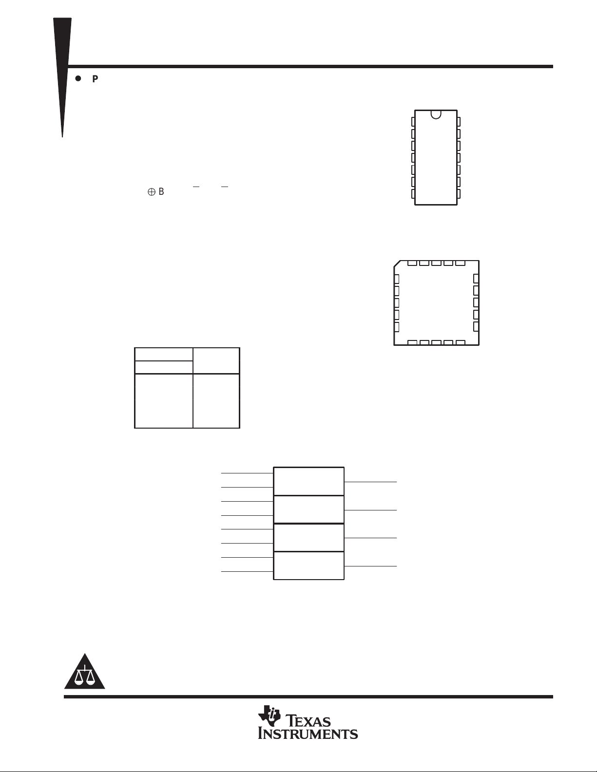
Package Options Include Plastic
Small-Outline (D) Thin Shrink Small-Outline
(PW), and Ceramic Flat (W) Packages,
Ceramic Chip Carriers (FK), and Standard
Plastic (N) and Ceramic (J) DIPs
description
These devices contain four independent 2-input
exclusive-OR gates. They perform the Boolean
function Y = A ę B or Y = AB + AB in positive logic.
A common application is as a true / complement
element. If one of the inputs is low, the other input
is reproduced in true form at the output. If one of
the inputs is high, the signal on the other input is
reproduced inverted at the output.
The SN54HC86 is characterized for operation
over the full military temperature range of –55°C
to 125°C. The SN74HC86 is characterized for
operation from –40°C to 85°C.
FUNCTION TABLE
(each gate)
INPUTS
A B
L L L
L HH
H LH
H H L
OUTPUT
Y
SN54HC86 ...J OR W PACKAGE
SN74HC86 . . . D, N, OR PW PACKAGE
SN54HC86 . . . FK PACKAGE
1Y
NC
2A
NC
2B
NC – No internal connection
(TOP VIEW)
1A
1
1B
2
1Y
3
2A
4
2B
5
2Y
6
GND
7
(TOP VIEW)
1B1ANC
3212019
4
5
6
7
8
910111213
2Y
GND
NC
14
13
12
11
10
9
8
V
3Y
CC
V
4B
4A
4Y
3B
3A
3Y
4B
18
17
16
15
14
3A
CC
4A
NC
4Y
NC
3B
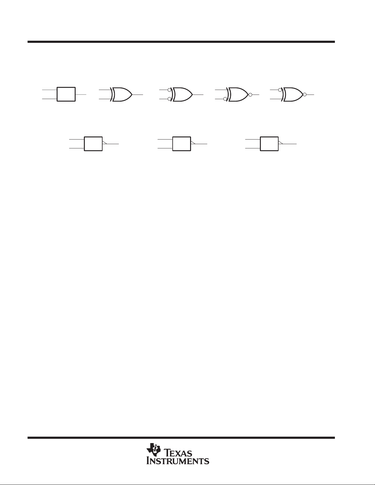
logic symbol
†
This symbol is in accordance with ANSI/IEEE Std 91-1984 and IEC Publication 617-12.
Pin numbers shown are for the D, J, N, PW, and W packages.
PRODUCTION DATA information is current as of publication date.
Products conform to specifications per the terms of Texas Instruments
standard warranty. Production processing does not necessarily include
testing of all parameters.
†
1
1A
2
1B
4
2A
5
2B
9
3A
10
3B
12
4A
13
4B
Please be aware that an important notice concerning availability, standard warranty, and use in critical applications of
Texas Instruments semiconductor products and disclaimers thereto appears at the end of this data sheet.
=1
3
1Y
6
2Y
8
3Y
11
4Y
Copyright 1999, Texas Instruments Incorporated
On products compliant to MIL-PRF-38535, all parameters are tested
unless otherwise noted. On all other products, production
processing does not necessarily include testing of all parameters.
POST OFFICE BOX 655303 • DALLAS, TEXAS 75265
1
SN54HC86, SN74HC86
QUADRUPLE 2-INPUT EXCLUSIVE-OR GATES
SCLS100C – DECEMBER 1982 – REVISED AUGUST 1999
exclusive-OR logic
An exclusive-OR gate has many applications, some of which can be represented better by alternative logic
symbols.
Exclusive OR
= 1
These are five equivalent exclusive-OR symbols valid for an ’HC86 gate in positive logic; negation may be
shown at any two ports.
Logic Identity Element Even-Parity Element Odd-Parity Element
= 2k 2k + 1
The output is active (low) if
all inputs stand at the same
logic level (i.e., A = B).
absolute maximum ratings over operating free-air temperature range
The output is active (low) if
an even number of inputs
(i.e., 0 or 2) are active.
The output is active (high) if
an odd number of inputs (i.e.,
only 1 of the 2) are active.
†
Supply voltage range, VCC –0.5 V to 7 V. . . . . . . . . . . . . . . . . . . . . . . . . . . . . . . . . . . . . . . . . . . . . . . . . . . . . . . . . .
Input clamp current, IIK (VI < 0 or VI > VCC) (see Note 1) ±20 mA. . . . . . . . . . . . . . . . . . . . . . . . . . . . . . . . . . . .
Output clamp current, IOK (VO < 0 or VO > VCC) (see Note 1) ±20 mA. . . . . . . . . . . . . . . . . . . . . . . . . . . . . . . .
Continuous output current, I
(VO = 0 to VCC) ±25 mA. . . . . . . . . . . . . . . . . . . . . . . . . . . . . . . . . . . . . . . . . . . . . .
O
Continuous current through VCC or GND ±50 mA. . . . . . . . . . . . . . . . . . . . . . . . . . . . . . . . . . . . . . . . . . . . . . . . . . .
Package thermal impedance, θ
(see Note 2): D package 127°C/W. . . . . . . . . . . . . . . . . . . . . . . . . . . . . . . . . .
JA
N package 78°C/W. . . . . . . . . . . . . . . . . . . . . . . . . . . . . . . . . . .
PW package 170°C/W. . . . . . . . . . . . . . . . . . . . . . . . . . . . . . . .
Storage temperature range, T
†
Stresses beyond those listed under “absolute maximum ratings” may cause permanent damage to the device. These are stress ratings only, and
functional operation of the device at these or any other conditions beyond those indicated under “recommended operating conditions” is not
implied. Exposure to absolute-maximum-rated conditions for extended periods may affect device reliability.
NOTES: 1. The input and output voltage ratings may be exceeded if the input and output current ratings are observed.
2. The package thermal impedance is calculated in accordance with JESD 51, except for through-hole packages, which use a trace
length of zero.
–65°C to 150°C. . . . . . . . . . . . . . . . . . . . . . . . . . . . . . . . . . . . . . . . . . . . . . . . . . .
stg
2
POST OFFICE BOX 655303 • DALLAS, TEXAS 75265
 Loading...