

SN54HC166, SN74HC166
8-BIT PARALLEL-LOAD SHIFT REGISTERS
SCLS117B – DECEMBER 1982 – REVISED MAY 1997
1
POST OFFICE BOX 655303 • DALLAS, TEXAS 75265
D
Synchronous Load
D
Direct Overriding Clear
D
Parallel-to-Serial Conversion
D
Package Options Include Plastic
Small-Outline (D) and Ceramic Flat (W)
Packages, Ceramic Chip Carriers (FK), and
Standard Plastic (N) and Ceramic (J)
300-mil DIPs
description
The ’HC166 parallel-in or serial-in, serial-out
registers feature gated clock (CLK, CLK INH)
inputs and an overriding clear (CLR) input. The
parallel-in or serial-in modes are established by
the shift / load (SH/LD
) input. When high, SH/LD
enables the serial (SER) data input and couples
the eight flip-flops for serial shifting with each
clock (CLK) pulse. When low, the parallel
(broadside) data inputs are enabled, and
synchronous loading occurs on the next clock
pulse. During parallel loading, serial data flow is
inhibited. Clocking is accomplished on the
low-to-high-level edge of CLK through a 2-input
positive-NOR gate permitting one input to be used
as a clock-enable or clock-inhibit function. Holding
either CLK or CLK INH high inhibits clocking;
holding either low enables the other clock input.
This allows the system clock to be free running,
and the register can be stopped on command with
the other clock input. CLK INH should be changed
to the high level only when CLK is high. CLR
overrides all other inputs, including CLK, and
resets all flip-flops to zero.
The SN54HC166 is characterized for operation over the full military temperature range of –55°C to 125°C. The
SN74HC166 is characterized for operation from –40°C to 85°C.
Please be aware that an important notice concerning availability, standard warranty, and use in critical applications of
Texas Instruments semiconductor products and disclaimers thereto appears at the end of this data sheet.
3212019
910111213
4
5
6
7
8
18
17
16
15
14
H
Q
H
NC
G
F
B
C
NC
D
CLK INH
A
SER
NC
CLR
E
V
SH/LD
CLK
GND
NC
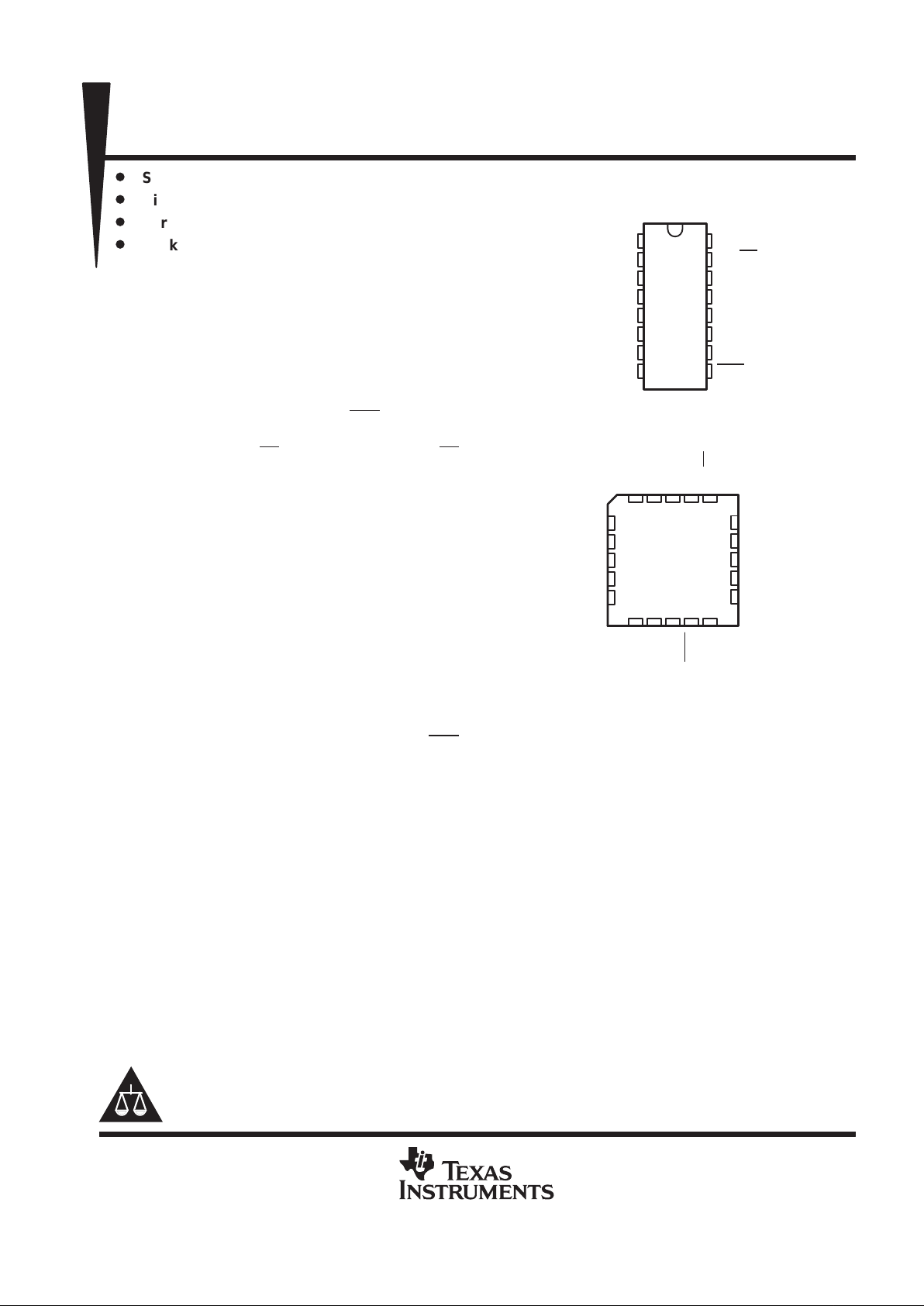
SN54HC166 ...FK PACKAGE
(TOP VIEW)
CC
NC – No internal connection
1
2
3
4
5
6
7
8
16
15
14
13
12
11
10
9
SER
A
B
C
D
CLK INH
CLK
GND
V
CC
SH/LD
H
Q
H
G
F
E
CLR
SN54HC166 ...J OR W PACKAGE
SN74HC166 . . . D OR N PACKAGE
(TOP VIEW)
Copyright 1997, Texas Instruments Incorporated
PRODUCTION DATA information is current as of publication date.
Products conform to specifications per the terms of Texas Instruments
standard warranty. Production processing does not necessarily include
testing of all parameters.
SN54HC166, SN74HC166
8-BIT PARALLEL-LOAD SHIFT REGISTERS
SCLS117B – DECEMBER 1982 – REVISED MAY 1997
2
POST OFFICE BOX 655303 • DALLAS, TEXAS 75265
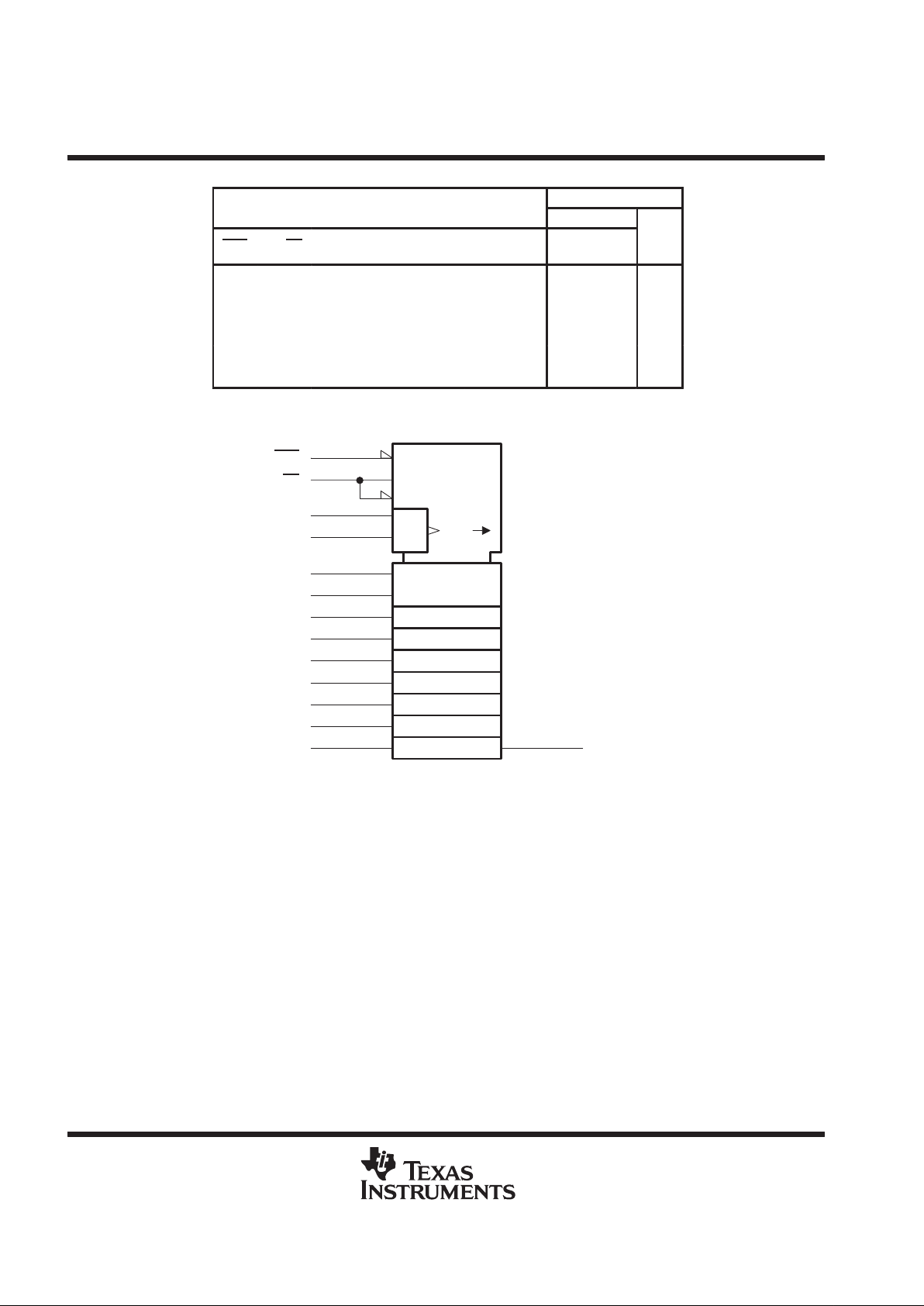
FUNCTION TABLE
OUTPUTS
INPUTS
INTERNAL
CLR SH/LD
CLK INH CLK SER
PARALLEL
A...H
Q
A
Q
B
Q
H
L X X X X X L L L
H XLLX XQA0Q
B0QH0
H LL↑ X a...h a bh
H HL↑ HXHQ
AnQGn
H HL↑ LXLQ
AnQGn
H X H ↑ X X Q
A0QB0QH0
logic symbol
†
CLR
SRG8
R
9
M1 [Shift]
15
M2 [Load]
6
CLK INH
7
CLK
C3/1
2, 3D
3
B
4
C
5
D
10
E
11
F
12
G
14
H
1, 3D
1
SER
2, 3D
2
A
13
≥1
Q
H
SH/LD
†
This symbol is in accordance with ANSI/IEEE Std 91-1984 and IEC Publication 617-12.
Pin numbers shown are for the D, J, N, and W packages.
SN54HC166, SN74HC166
8-BIT PARALLEL-LOAD SHIFT REGISTERS
SCLS117B – DECEMBER 1982 – REVISED MAY 1997
3
POST OFFICE BOX 655303 • DALLAS, TEXAS 75265
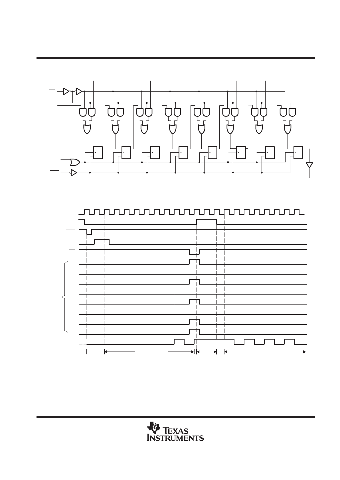
logic diagram (positive logic)
1D
C1
15
9
7
6
13
SH/LD
CLR
CLK
CLK INH
Q
H
234510111214
SER
ABCDEFGH
R
1D
C1
R
1D
C1
R
1D
C1
R
1D
C1
R
1D
C1
R
1D
C1
R
1D
C1
R
1
Pin numbers shown are for the D, J, N, and W packages.
typical clear, shift, load, inhibit, and shift sequence
Clear Load
Inhibit
H
H
H
H
H
H HHHH
LLL
L
L
L
CLK
CLK INH
SER
A
B
C
D
E
F
G
H
SH/LD
CLR
Q
H
Parallel
Inputs
Serial Shift Serial Shift
 Loading...