

Texas Instruments SN74BCT640DW, SN74BCT640DWR, SN74BCT640N, SNJ54BCT640FK, SNJ54BCT640J Datasheet
...
SN54BCT640, SN74BCT640
OPERATION
OCTAL BUS TRANSCEIVERS
WITH 3-STATE OUTPUTS
SCBS025C – SEPTEMBER 1988 – REVISED APRIL 1994
• State-of-the-Art BiCMOS Design
Substantially Reduces Standby Current
• Outputs Have Undershoot-Protection
Circuitry
• Power-Up High-Impedance State
• Buffered Control Inputs to Reduce DC
Loading Effects
• ESD Protection Exceeds 2000 V
Per MIL-STD-883C, Method 3015
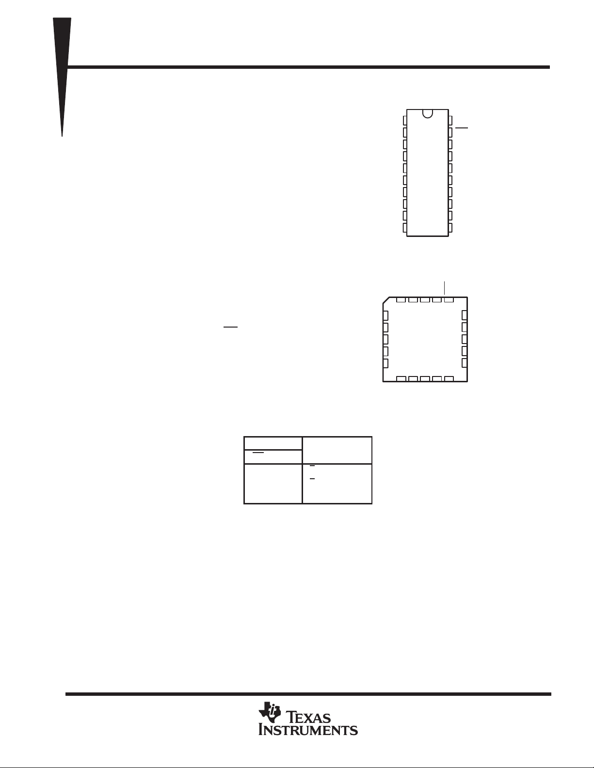
• Package Options Include Plastic
Small-Outline (DW) Packages, Ceramic
Chip Carriers (FK) and Flatpacks (W), and
Plastic and Ceramic 300-mil DIPs (J, N)
description
The ′BCT640 bus transceiver is designed for
asynchronous communication between data
buses. These devices transmit data from the A
bus to the B bus or from the B bus to the A bus
depending upon the level at the direction-control
(DIR) input. The output-enable (OE
used to disable the device so that the buses are
effectively isolated.
The SN54BCT640 is characterized for operation
over the full military temperature range of –55°C
to 125°C. The SN74BCT640 is characterized for
operation from 0°C to 70°C.
) input can be
SN54BCT640 ...J OR W PACKAGE
SN74BCT640 . . . DW OR N PACKAGE
SN54BCT640 . . . FK PACKAGE
A3
A4
A5
A6
A7
(TOP VIEW)
DIR
1
A1
2
A2
3
A3
4
A4
5
6
A5
7
A6
8
A7
9
A8
10
GND
(TOP VIEW)
A2A1DIR
3212019
4
5
6
7
8
9
10 11 12 13
A8
B8
20
19
18
17
16
15
14
13
12
11
V
CC
B7
18
17
16
15
14
B6 OE
V
OE
B1
B2
B3
B4
B5
B6
B7
B8
CC
B1
B2
B3
B4
B5
GND
PRODUCTION DATA information is current as of publication date.
Products conform to specifications per the terms of Texas Instruments
standard warranty. Production processing does not necessarily include
testing of all parameters.
FUNCTION TABLE
INPUTS
OE DIR
L L B data to A bus
L HA data to B bus
H X Isolation
Copyright 1994, Texas Instruments Incorporated
POST OFFICE BOX 655303 • DALLAS, TEXAS 75265
2–1
SN54BCT640, SN74BCT640
OCTAL BUS TRANSCEIVERS
WITH 3-STATE OUTPUTS
SCBS025C – SEPTEMBER 1988 – REVISED APRIL 1994
19
1
2
3
4
5
6
7
8
9
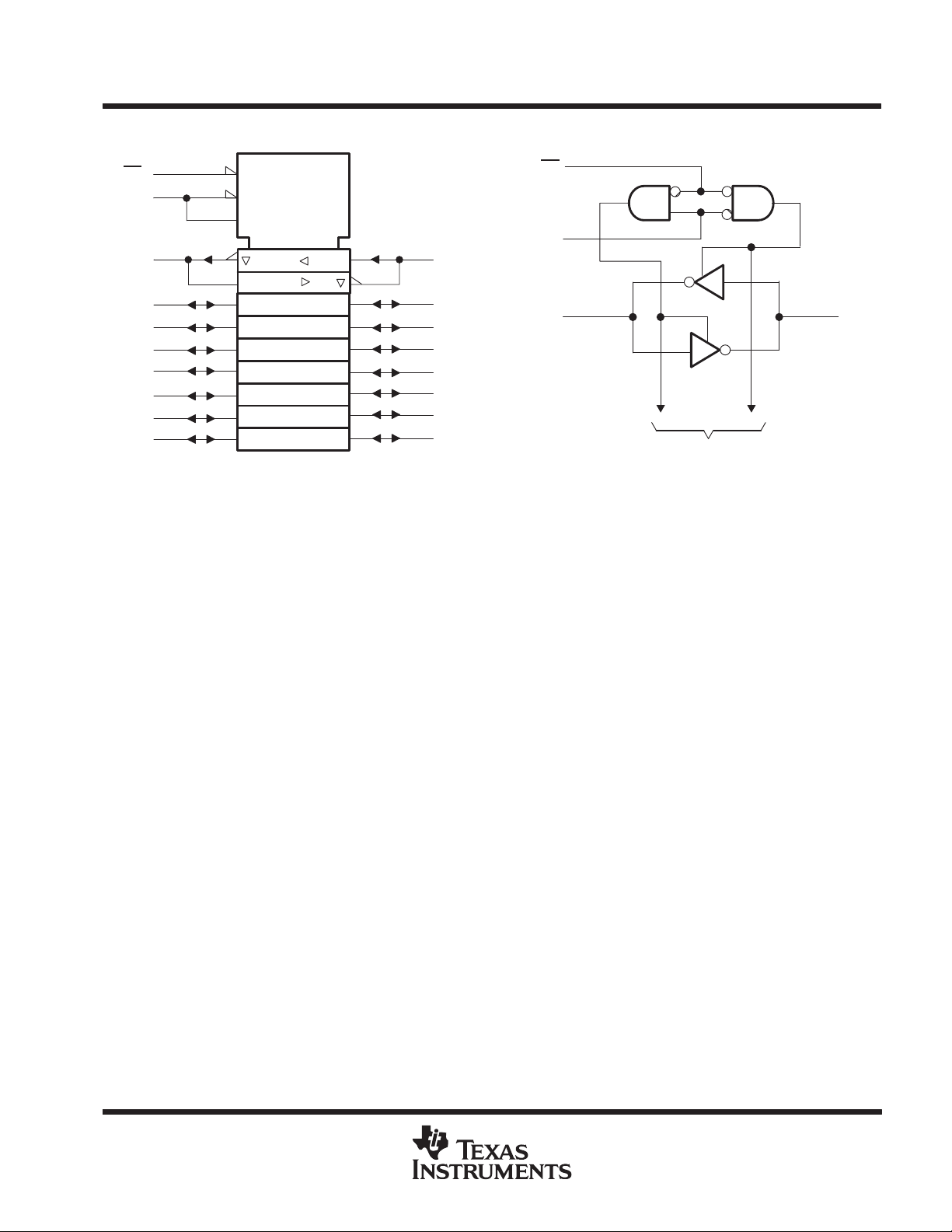
†
G3
3 EN1 [BA]
3 EN2 [AB]
1
1
1
logic diagram (positive logic)
19
OE
1
18
B1
2
17
16
15
14
13
12
11
B2
B3
B4
B5
B6
B7
B8
DIR
A1 B1
To Seven Other Channels
182
logic symbol
OE
DIR
A1
A2
A3
A4
A5
A6
A7
A8
†
This symbol is in accordance with ANSI/IEEE Std 91-1984
and IEC Publication 617-12.
absolute maximum ratings over operating free-air temperature range (unless otherwise noted)
Supply voltage range, V
CC
Input voltage range: Control inputs (see Note 1) – 0.5 V to 7 V. . . . . . . . . . . . . . . . . . . . . . . . . . . . . . . . . . . . . . . .
I/O ports (see Note 1) – 0.5 V to 5.5 V. . . . . . . . . . . . . . . . . . . . . . . . . . . . . . . . . . . . . . . . . .
Voltage range applied to any output in the disabled or power-off state, V
Voltage range applied to any output in the high state, V
. . . . . . . . . . . . . . . . . . . . . . . . . . . . . . .
O
O
Input clamp current, IIK –30 mA. . . . . . . . . . . . . . . . . . . . . . . . . . . . . . . . . . . . . . . . . . . . . . . . . . . . . . . . . . . . . . . . . .
Current into any output in the low state: SN54BCT640 96 mA. . . . . . . . . . . . . . . . . . . . . . . . . . . . . . . . . . . . . . . .
SN74BCT640 128 mA. . . . . . . . . . . . . . . . . . . . . . . . . . . . . . . . . . . . . . .
Operating free-air temperature range: SN54BCT640 – 55°C to 125°C. . . . . . . . . . . . . . . . . . . . . . . . . . . . . . . .
SN74BCT640 0°C to 70°C. . . . . . . . . . . . . . . . . . . . . . . . . . . . . . . . . . . .
Storage temperature range – 65°C to 150°C. . . . . . . . . . . . . . . . . . . . . . . . . . . . . . . . . . . . . . . . . . . . . . . . . . . . . . . .
‡
Stresses beyond those listed under “absolute maximum ratings” may cause permanent damage to the device. These are stress ratings only, and
functional operation of the device at these or any other conditions beyond those indicated under “recommended operating conditions” is not
implied. Exposure to absolute-maximum-rated conditions for extended periods may affect device reliability.
NOTE 1: The input and output voltage ratings may be exceeded if the input and output current ratings are observed.
– 0.5 V to 7 V. . . . . . . . . . . . . . . . . . . . . . . . . . . . . . . . . . . . . . . . . . . . . . . . . . . . . . . . . .
– 0.5 V to 5.5 V. . . . . . . . . . . . . . .
– 0.5 V to V
‡
CC
2–2
POST OFFICE BOX 655303 • DALLAS, TEXAS 75265
 Loading...