


SN54BCT544, SN74BCT544
OCTAL REGISTERED TRANSCEIVERS
WITH 3-STATE OUTPUTS
SCBS039B – NOVEMBER 1988 – REVISED NOVEMBER 1993
Copyright 1993, Texas Instruments Incorporated
1
POST OFFICE BOX 655303 • DALLAS, TEXAS 75265
• State-of-the-Art BiCMOS Design
Significantly Reduces I
CCZ
• ESD Protection Exceeds 2000 V
Per MIL-STD-883C, Method 3015
• Power-Up High-Impedance State
• 3-State Inverting Outputs
• Back-to-Back Registers for Storage
• Package Options Include Plastic
Small-Outline (DW) Packages, Ceramic
Chip Carriers (FK) and Flatpacks (W), and
Plastic and Ceramic 300-mil DIPs (JT, NT)
description
The ′BCT544 octal registered transceiver
contains two sets of D-type latches for temporary
storage of data flowing in either direction.
Separate latch-enable (LEAB
or LEBA) and
output-enable (OEAB or OEBA) inputs are
provided for each register to permit independent
control in either direction of data flow.
The A-to-B enable (CEAB) input must be low in
order to enter data from A or to output data from
B. If CEAB is low and LEAB is low, the A-to-B
latches are transparent; a subsequent low-to-high
transition of LEAB
puts the A latches in the storage
mode. With CEAB and OEAB both low, the 3-state
B outputs are active and reflect the inverted data
present at the output of the A latches. Data flow
from B to A is similar, but requires using the CEBA,
LEBA
, and OEBA inputs.
The SN54BCT544 is characterized for operation
over the full military temperature range of –55°C
to 125°C. The SN74BCT544 is characterized for
operation from 0°C to 70°C.
FUNCTION TABLE
†
INPUTS
OUTPUT
CEAB LEAB OEAB A
B
H X X X Z
L XHX Z
L HLX B
0
‡
L LLL H
L L L H L
†
A-to-B data flow is shown; B-to-A flow control is the same
except that it uses CEBA
, LEBA, and OEBA.
‡
Output level before the indicated steady-state input
conditions were established.
SN54BCT544 . . . JT OR W PACKAGE
SN74BCT544 . . . DW OR NT PACKAGE
(TOP VIEW)
1
2
3
4
5
6
7
8
9
10
11
12
24
23
22
21
20
19
18
17
16
15
14
13
LEBA
OEBA
A1
A2
A3
A4
A5
A6
A7
A8
CEAB
GND
V
CC
CEBA
B1
B2
B3
B4
B5
B6
B7
B8
LEAB
OEAB
SN54BCT544 . . . FK PACKAGE
(TOP VIEW)
3212827
12 13
5
6
7
8
9
10
11
25
24
23
22
21
20
19
B2
B3
B4
NC
B5
B6
B7
A2
A3
A4
NC
A5
A6
A7
426
14 15 16 1718
A8
CEAB
GND
NC
OEAB
LEAB
B8
A1
OEBA
LEBANCCEBA
B1
V
CC
NC – No internal connection
PRODUCTION DATA information is current as of publication date.
Products conform to specifications per the terms of Texas Instruments
standard warranty. Production processing does not necessarily include
testing of all parameters.
SN54BCT544, SN74BCT544
OCTAL REGISTERED TRANSCEIVERS
WITH 3-STATE OUTPUTS
SCBS039B – NOVEMBER 1988 – REVISED NOVEMBER 1993
2
POST OFFICE BOX 655303 • DALLAS, TEXAS 75265
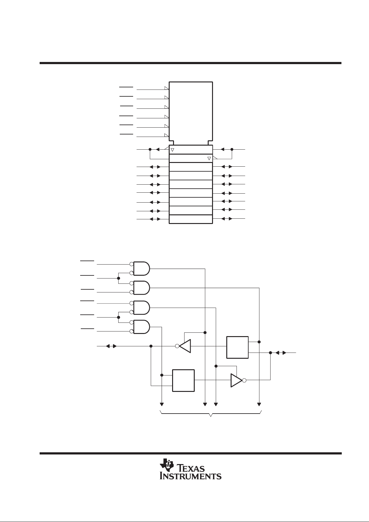
logic symbol
†
4
2C6
14
3
A1
4
A2
B1
22
5D
5
A3
6
A4
7
A5
8
A6
9
A7
10
A8
B2
21
B3
20
B5
18
B4
19
B6
17
B8
15
B7
16
LEAB
3
G2
11
CEAB
2EN4
13
OEAB
1C5
1
LEBA
G1
23
CEBA
1EN3
2
OEBA
6D
†
This symbol is in accordance with ANSI/IEEE Std 91-1984 and IEC Publication 617-12.
logic diagram (positive logic)
OEBA
CEBA
LEBA
OEAB
CEAB
LEAB
A1
B1
C1
1D
C1
1D
2
23
1
13
11
14
3
22
To Seven Other Channels
Pin numbers shown are for the DW, JT, NT, and W packages.
 Loading...