

Texas Instruments SN74BCT541ADW, SN74BCT541ADWR, SN74BCT541AN, SNJ54BCT541FK, SNJ54BCT541J Datasheet
...
SN54BCT541, SN74BCT541A
OCTAL BUFFERS/DRIVERS
WITH 3-STATE OUTPUTS
SCBS011D – JULY 1988 – REVISED SEPTEMBER 1994
• State-of-the-Art BiCMOS Design
Significantly Reduces I
CCZ
• 3-State Outputs Drive Bus Lines or Buffer
Memory-Address Registers
• P-N-P Inputs Reduce DC Loading
• Data Flow-Through Pinout (All Inputs on
Opposite Side From Outputs)
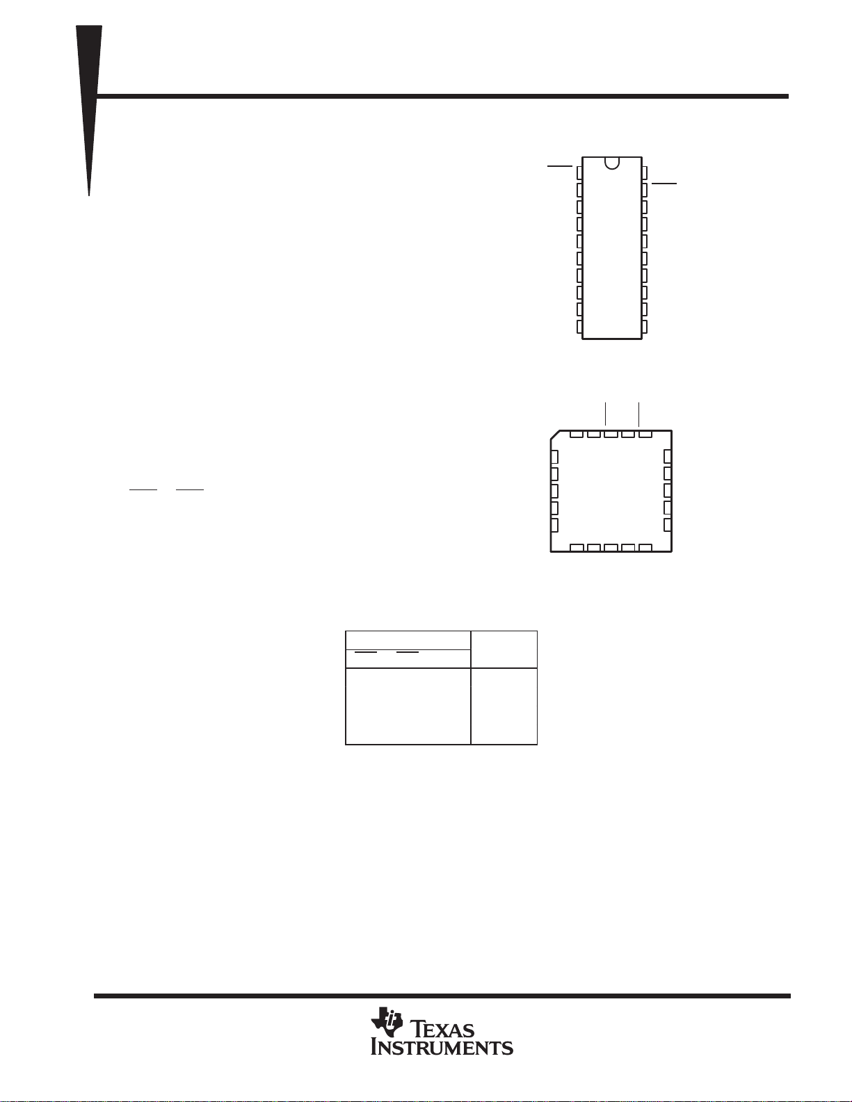
• Package Options Include Plastic
Small-Outline (DW) Packages, Ceramic
Chip Carriers (FK) and Flatpacks (W), and
Plastic (N) and Ceramic (J) 300-mil DIPs
description
The SN54BCT541 and SN74BCT541A octal
buffers and line drivers are ideal for driving bus
lines or buffering memory-address registers. The
devices feature inputs and outputs on opposite
sides of the package to facilitate printed-circuitboard layout.
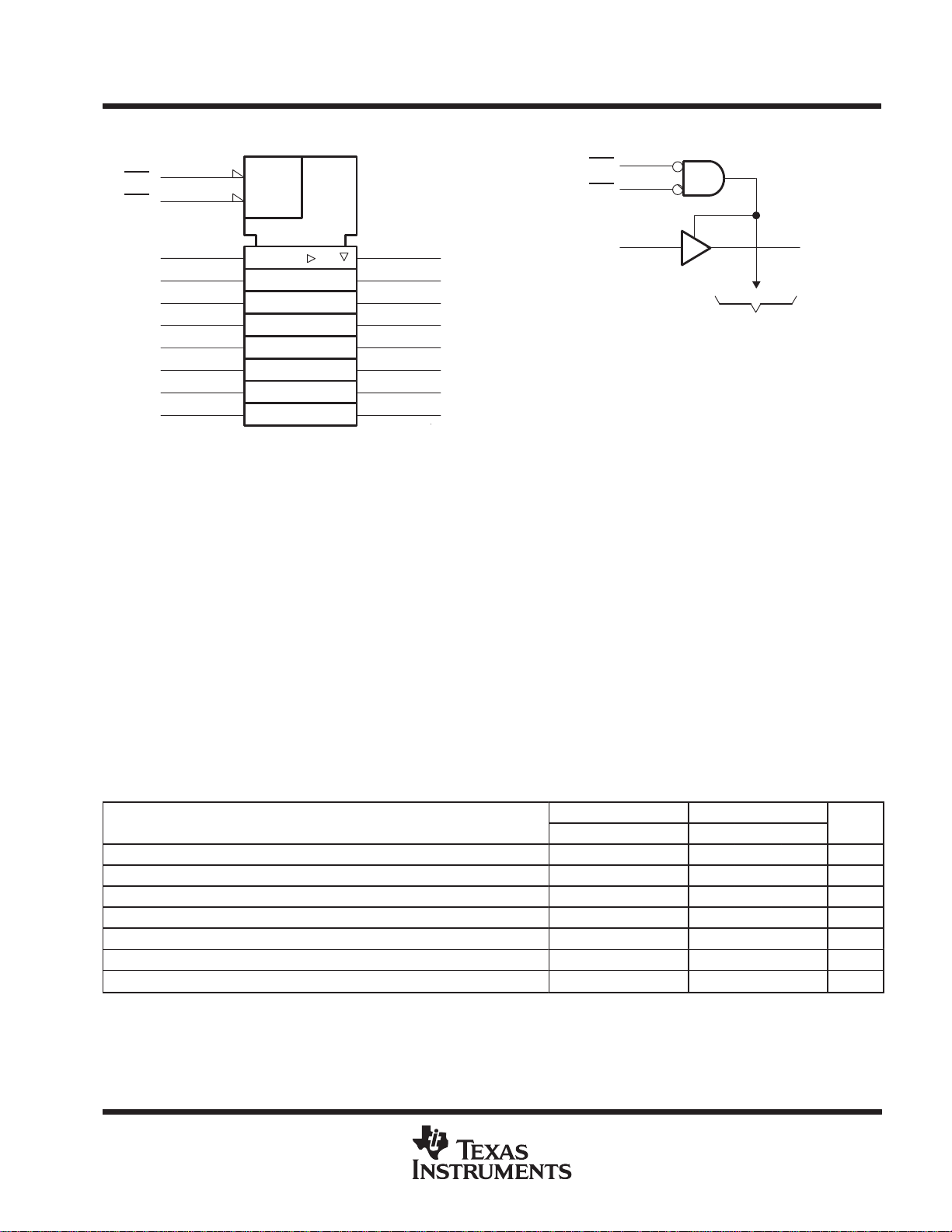
The 3-state control gate is a 2-input AND gate with
active-low inputs so that if either output-enable
(OE1
or OE2) input is high, all eight outputs are in
the high-impedance state.
The SN54BCT541 is characterized for operation
over the full military temperature range of –55°C
to 125°C. The SN74BCT541A is characterized for
operation from 0°C to 70°C.
SN54BCT541 ...J OR W PACKAGE
SN74BCT541A . . . DW OR N PACKAGE
SN54BCT541 . . . FK PACKAGE
A3
A4
A5
A6
A7
(TOP VIEW)
OE1
1
A1
2
A2
3
A3
4
A4
5
6
A5
7
A6
8
A7
9
A8
GND
10
(TOP VIEW)
A2A1OE1
3212019
4
5
6
7
8
9 10 11 12 13
A8
Y8
20
19
18
17
16
15
14
13
12
11
V
Y7
CC
V
CC
OE2
Y1
Y2
Y3
Y4
Y5
Y6
Y7
Y8
18
17
16
15
14
Y6 OE2
Y1
Y2
Y3
Y4
Y5
GND
PRODUCTION DATA information is current as of publication date.
Products conform to specifications per the terms of Texas Instruments
standard warranty. Production processing does not necessarily include
testing of all parameters.
FUNCTION TABLE
INPUTS
OE1 OE2 A
L L L L
L LH H
H XX Z
X H X Z
OUTPUT
Y
Copyright 1994, Texas Instruments Incorporated
POST OFFICE BOX 655303 • DALLAS, TEXAS 75265
1
SN54BCT541, SN74BCT541A
UNIT
OCTAL BUFFERS/DRIVERS
WITH 3-STATE OUTPUTS
SCBS011D – JULY 1988 – REVISED SEPTEMBER 1994
1
19
2
3
4
5
6
7
8
9
†
&
EN
1
18
17
16
15
14
13
12
11
logic diagram (positive logic)
OE1
OE2
Y1
Y2
Y3
Y4
Y5
Y6
Y7
Y8
1
19
2
A1 Y1
18
To Seven Other Channels
logic symbol
OE1
OE2
A1
A2
A3
A4
A5
A6
A7
A8
†
This symbol is in accordance with ANSI/IEEE Std 91-1984
and IEC Publication 617-12.
absolute maximum ratings over operating free-air temperature range (unless otherwise noted)
Supply voltage range, V
CC
Input voltage range, VI (see Note 1) – 0.5 V to 7 V. . . . . . . . . . . . . . . . . . . . . . . . . . . . . . . . . . . . . . . . . . . . . . . . . . .
Voltage range applied to any output in the disabled or power-off state, V
Voltage range applied to any output in the high state, V
– 0.5 V to V
. . . . . . . . . . . . . . . . . . . . . . . . . . . . . . .
O
O
Current into any output in the low state: SN54BCT541 96 mA. . . . . . . . . . . . . . . . . . . . . . . . . . . . . . . . . . . . . . . .
SN74BCT541A 128 mA. . . . . . . . . . . . . . . . . . . . . . . . . . . . . . . . . . . . . .
Operating free-air temperature range, TA: SN54BCT541 – 55°C to 125°C. . . . . . . . . . . . . . . . . . . . . . . . . . . . . .
SN74BCT541A 0°C to 70°C. . . . . . . . . . . . . . . . . . . . . . . . . . . . . . . . .
Storage temperature range – 65°C to 150°C. . . . . . . . . . . . . . . . . . . . . . . . . . . . . . . . . . . . . . . . . . . . . . . . . . . . . . . .
‡
Stresses beyond those listed under “absolute maximum ratings” may cause permanent damage to the device. These are stress ratings only, and
functional operation of the device at these or any other conditions beyond those indicated under “recommended operating conditions” is not
implied. Exposure to absolute-maximum-rated conditions for extended periods may affect device reliability.
NOTE 1: The input and output voltage ratings may be exceeded if the input and output current ratings are observed.
– 0.5 V to 7 V. . . . . . . . . . . . . . . . . . . . . . . . . . . . . . . . . . . . . . . . . . . . . . . . . . . . . . . . . .
– 0.5 V to 5.5 V. . . . . . . . . . . . . . .
‡
CC
recommended operating conditions
2
V
V
V
I
I
I
T
CC
IH
IL
IK
OH
OL
A
Supply voltage 4.5 5 5.5 4.5 5 5.5 V
High-level input voltage 2 2 V
Low-level input voltage 0.8 0.8 V
Input clamp current –18 –18 mA
High-level output current –12 –15 mA
Low-level output current 48 64 mA
Operating free-air temperature –55 125 0 70 °C
POST OFFICE BOX 655303 • DALLAS, TEXAS 75265
SN54BCT541 SN74BCT541A
MIN NOM MAX MIN NOM MAX
 Loading...