

Texas Instruments SN74BCT2240DBLE, SN74BCT2240DBR, SN74BCT2240DW, SN74BCT2240DWR, SN74BCT2240N Datasheet
...
SN54BCT2240, SN74BCT2240
OCTAL BUFFERS AND LINE/MOS DRIVERS
WITH 3-STATE OUTPUTS
SCBS030D – SEPTEMBER 1988 – REVISED APRIL 1994
Copyright 1994, Texas Instruments Incorporated
2–1
POST OFFICE BOX 655303 • DALLAS, TEXAS 75265
• State-of-the-Art BiCMOS Design
Significantly Reduces I
CCZ
• Output Ports Have Equivalent 33-Ω Series
Resistors, So No External Resistors Are
Required
• 3-State Outputs Drive Bus Lines or Buffer
Memory Address Registers
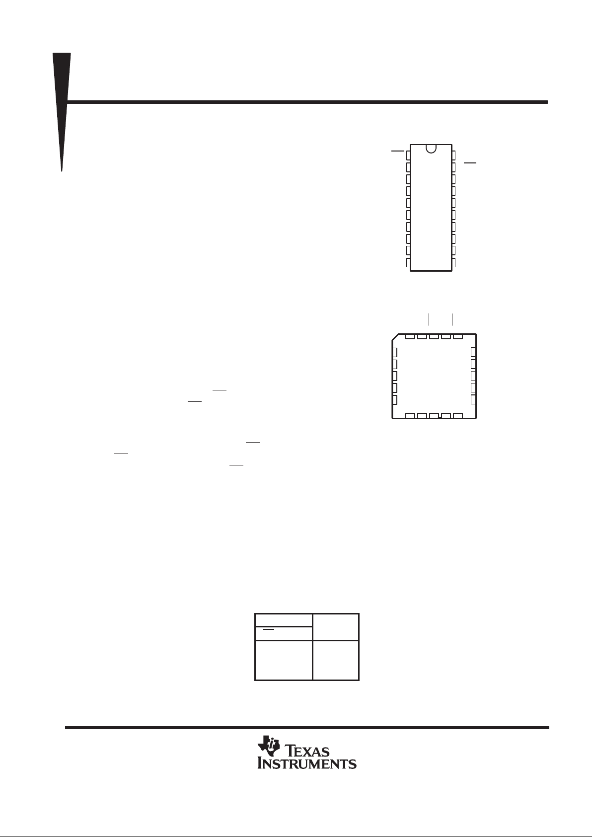
• Package Options Include Plastic
Small-Outline (DW) and Shrink
Small-Outline (DB) Packages, Ceramic Chip
Carriers (FK) and Flatpacks (W), and
Standard Plastic and Ceramic 300-mil DIPs
(J, N)
description
These octal buffers and line drivers are designed
specifically to improve both the performance and
density of 3-state memory address drivers, clock
drivers, and bus-oriented receivers and
transmitters. Taken together with the
SN74BCT2241 and ′BCT2244, these devices
provide the choice of selected combinations of
inverting and noninverting outputs, symmetrical
active-low output-enable (OE
) inputs, and
complementary OE and OE inputs. These devices
feature high fan-out and improved fan-in.
The ′BCT2240 is organized as two 4-bit line
drivers with separate output-enable (OE) inputs.
When OE is low, the device passes data from the
A inputs to the Y outputs. When OE
is high, the
outputs are in the high-impedance state.
The outputs, which are designed to source or sink
up to 12 mA, include 33-Ω series resistors to
reduce overshoot and undershoot.
The SN54BCT2240 is characterized for operation
over the full military temperature range of –55°C
to 125°C. The SN74BCT2240 is characterized for
operation from 0°C to 70°C.
FUNCTION TABLE
(each buffer)
INPUTS
OUTPUT
OE
A
Y
L H L
L LH
H X Z
1
2
3
4
5
6
7
8
9
10
20
19
18
17
16
15
14
13
12
11
1OE
1A1
2Y4
1A2
2Y3
1A3
2Y2
1A4
2Y1
GND
V
CC
2OE
1Y1
2A4
1Y2
2A3
1Y3
2A2
1Y4
2A1
SN54BCT2240 ...J OR W PACKAGE
SN74BCT2240 . . . DB, DW, OR N PACKAGE
(TOP VIEW)
3212019
910111213
4
5
6
7
8
18
17
16
15
14
1Y1
2A4
1Y2
2A3
1Y3
1A2
2Y3
1A3
2Y2
1A4
SN54BCT2240 . . . FK PACKAGE
(TOP VIEW)
2Y4
1A1
1OE
1Y4
2A2 2OE
2Y1
GND
2A1
V
CC
PRODUCTION DATA information is current as of publication date.
Products conform to specifications per the terms of Texas Instruments
standard warranty. Production processing does not necessarily include
testing of all parameters.
SN54BCT2240, SN74BCT2240
OCTAL BUFFERS AND LINE/MOS DRIVERS
WITH 3-STATE OUTPUTS
SCBS030D – SEPTEMBER 1988 – REVISED APRIL 1994
2–2
POST OFFICE BOX 655303 • DALLAS, TEXAS 75265
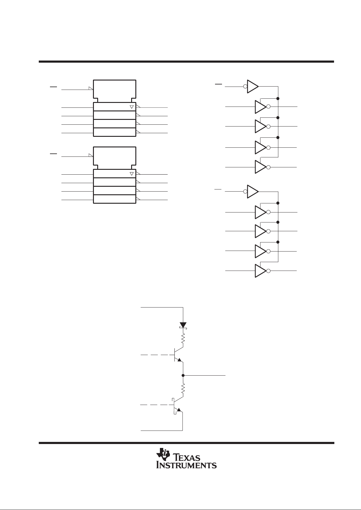
logic symbol
†
logic diagram (positive logic)
1OE
2
1A1
4
1A2
6
1A3
8
1A4
EN
1
1Y1
18
1Y2
16
1Y3
14
1Y4
12
2OE
11
2A1
13
2A2
15
2A3
17
2A4
EN
19
2Y1
9
2Y2
7
2Y3
5
2Y4
3
1
2
4
6
8
19
11
13
15
17
3
5
7
9
12
14
16
18
1A1
1A2
1A3
1A4
1Y1
2A1
2A2
2A3
2A4
2Y1
1Y2
1Y3
1Y4
2Y2
2Y3
2Y4
1OE
2OE
schematic of Y outputs
Output
V
CC
GND
1
1
†
This symbol is in accordance with ANSI/IEEE Std 91-1984
and IEC Publication 617-12.
 Loading...