

Texas Instruments SN74AS808BN3, SN74AS808BDW, SN74AS808BDWR, SN74AS808BN, SNJ54AS808BJ Datasheet
...
SN54AS808B, SN74AS808B
HEX 2-INPUT AND DRIVERS
SDAS018C – DECEMBER 1982 – REVISED JANUARY 1995
Copyright 1995, Texas Instruments Incorporated
1
POST OFFICE BOX 655303 • DALLAS, TEXAS 75265
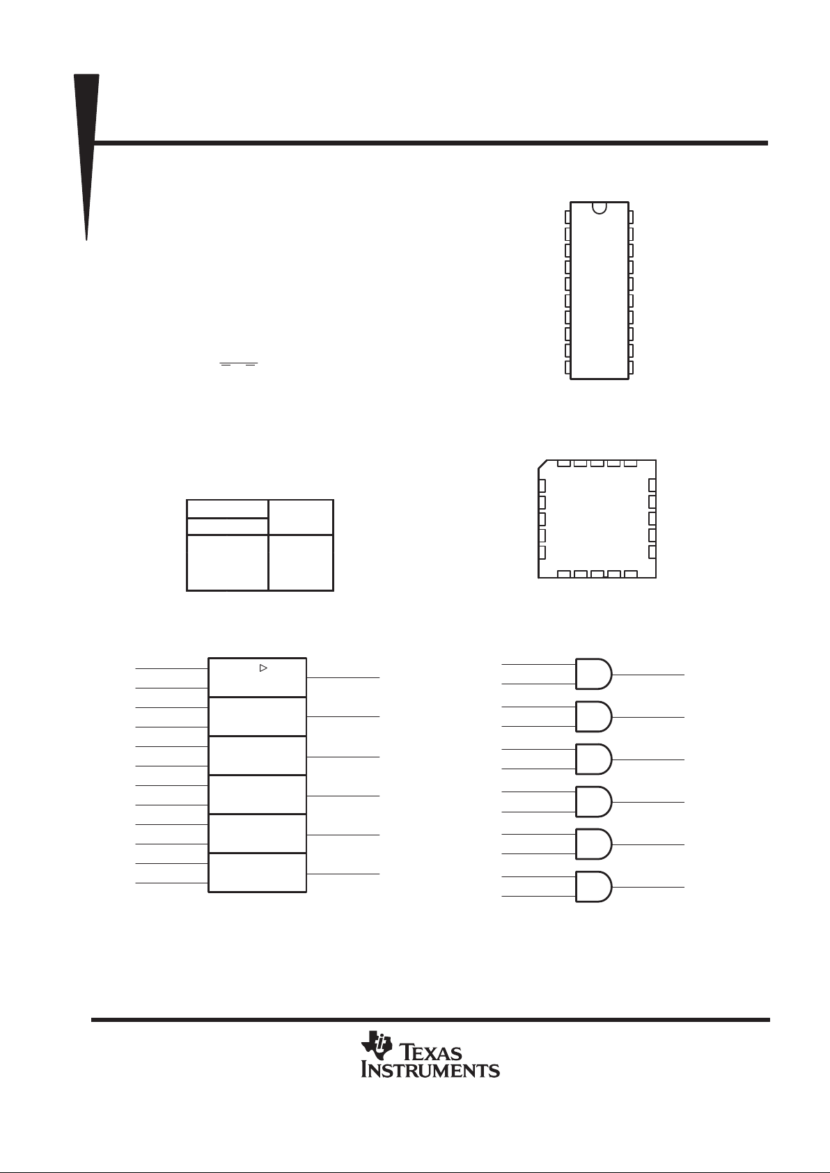
• High Capacitive-Drive Capability
• Typical Delay Time of 3.2 ns (C
L
= 50 pF)
and Typical Power Dissipation of Less
Than 13 mW Per Gate
• Package Options Include Plastic
Small-Outline (DW) Packages, Ceramic
Chip Carriers (FK), and Standard Plastic (N)
and Ceramic (J) 300-mil DIPs
description
These devices contain six independent 2-input
AND drivers. They perform the Boolean functions
Y = A • B or Y = A
+ B in positive logic.
The SN54AS808B is characterized for operation
over the full military temperature range of –55°C
to 125°C. The SN74AS808B is characterized for
operation from 0°C to 70°C.
FUNCTION TABLE
(each driver)
INPUTS
OUTPUT
A B
Y
H H H
L XL
XLL
logic symbol
†
logic diagram (positive logic)
1
1A
2
1B
4
2A
5
2B
7
3A
8
3B
12
4A
13
4B
&
1Y
3
2Y
6
3Y
9
4Y
11
15
5A
16
5B
18
6A
19
6B
5Y
14
6Y
17
1Y
3
1
1A
2
1B
2Y
6
4
2A
5
2B
3Y
9
7
3A
8
3B
4Y
11
12
4A
13
4B
5Y
14
15
5A
16
5B
6Y
17
18
6A
19
6B
†
This symbol is in accordance with ANSI/IEEE Std 91-1984 and
IEC Publication 617-12.
1
2
3
4
5
6
7
8
9
10
20
19
18
17
16
15
14
13
12
11
1A
1B
1Y
2A
2B
2Y
3A
3B
3Y
GND
V
CC
6B
6A
6Y
5B
5A
5Y
4B
4A
4Y
SN54AS808B ...J PACKAGE
SN74AS808B . . . DW OR N PACKAGE
(TOP VIEW)
3 2 1 20 19
910111213
4
5
6
7
8
18
17
16
15
14
6A
6Y
5B
5A
5Y
2A
2B
2Y
3A
3B
SN54AS808B . . . FK PACKAGE
(TOP VIEW)
1Y1B1A
4A
4B 6B
3Y
GND
4Y
V
CC
PRODUCTION DATA information is current as of publication date.
Products conform to specifications per the terms of Texas Instruments
standard warranty. Production processing does not necessarily include
testing of all parameters.
SN54AS808B, SN74AS808B
HEX 2-INPUT AND DRIVERS
SDAS018C – DECEMBER 1982 – REVISED JANUARY 1995
2
POST OFFICE BOX 655303 • DALLAS, TEXAS 75265
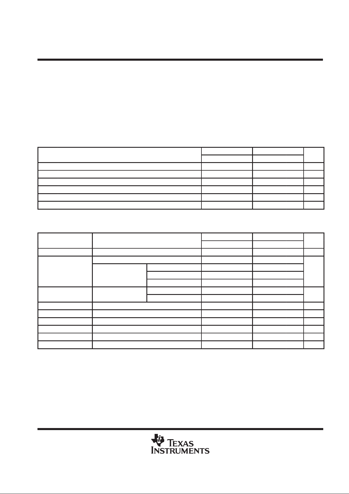
absolute maximum ratings over operating free-air temperature range (unless otherwise noted)
†
Supply voltage, V
CC
7 V. . . . . . . . . . . . . . . . . . . . . . . . . . . . . . . . . . . . . . . . . . . . . . . . . . . . . . . . . . . . . . . . . . . . . . . .
Input voltage, V
I
7 V. . . . . . . . . . . . . . . . . . . . . . . . . . . . . . . . . . . . . . . . . . . . . . . . . . . . . . . . . . . . . . . . . . . . . . . . . . . .
Operating free-air temperature range, T
A
: SN54AS808B –55°C to 125°C. . . . . . . . . . . . . . . . . . . . . . . . . . . . .
SN74AS808B 0°C to 70°C. . . . . . . . . . . . . . . . . . . . . . . . . . . . . . . . .
Storage temperature range –65°C to 150°C. . . . . . . . . . . . . . . . . . . . . . . . . . . . . . . . . . . . . . . . . . . . . . . . . . . . . . .
†
Stresses beyond those listed under “absolute maximum ratings” may cause permanent damage to the device. These are stress ratings only, and
functional operation of the device at these or any other conditions beyond those indicated under “recommended operating conditions” is not
implied. Exposure to absolute-maximum-rated conditions for extended periods may affect device reliability.
recommended operating conditions
SN54AS808B SN74AS808B
MIN NOM MAX MIN NOM MAX
UNIT
V
CC
Supply voltage 4.5 5 5.5 4.5 5 5.5 V
V
IH
High-level input voltage 2 2 V
V
IL
Low-level input voltage 0.8 0.8 V
I
OH
High-level output current –40 –48 mA
I
OL
Low-level output current 40 48 mA
T
A
Operating free-air temperature –55 125 0 70 °C
electrical characteristics over recommended operating free-air temperature range (unless
otherwise noted)
SN54AS808B SN74AS808B
PARAMETER
TEST CONDITIONS
MIN TYP‡MAX MIN TYP‡MAX
UNIT
V
IK
VCC = 4.5 V, II = –18 mA –1.2 –1.2 V
VCC = 4.5 V to 5.5 V, IOH = –2 mA VCC –2 VCC –2
IOH = –3 mA 2.4 3.2 2.4 3.2
V
OH
VCC = 4.5 V
IOH = –40 mA 2
V
IOH = –48 mA 2
IOL = 40 mA 0.25 0.5
V
OL
V
CC
= 4.5
V
IOL = 48 mA 0.35 0.5
V
I
I
VCC = 5.5 V, VI = 7 V 0.1 0.1 mA
I
IH
VCC = 5.5 V, VI = 2.7 V 20 20 µA
I
IL
VCC = 5.5 V, VI = 0.4 V –0.5 –0.5 mA
I
O
§
VCC = 5.5 V, VO = 2.25 V –50 –200 –50 –200 mA
I
CCH
VCC = 5.5 V, VI = 4.5 V 8 13 8 13 mA
I
CCL
VCC = 5.5 V, VI = 0 20 33 20 33 mA
‡
All typical values are at VCC = 5 V, TA = 25°C.
§
The output conditions have been chosen to produce a current that closely approximates one half of the true short-circuit output current, IOS.
 Loading...