

Texas Instruments SN74ALS760DW, SN74ALS760DWR, SN74ALS760N, SN74AS760DW, SN74AS760DWR Datasheet
...
SN54AS760, SN74ALS760, SN74AS760
OCTAL BUFFERS AND LINE DRIVERS
WITH OPEN-COLLECTOR OUTPUTS
SDAS141A – DECEMBER 1983 – REVISED JANUARY 1995
Copyright 1995, Texas Instruments Incorporated
1
POST OFFICE BOX 655303 • DALLAS, TEXAS 75265
• Open-Collector Outputs Drive Bus Lines or
Buffer Memory Address Registers
• Eliminates the Need for 3-State Overlap
Protection
• pnp Inputs Reduce dc Loading
• Open-Collector Versions of ′ALS244 and
′AS244
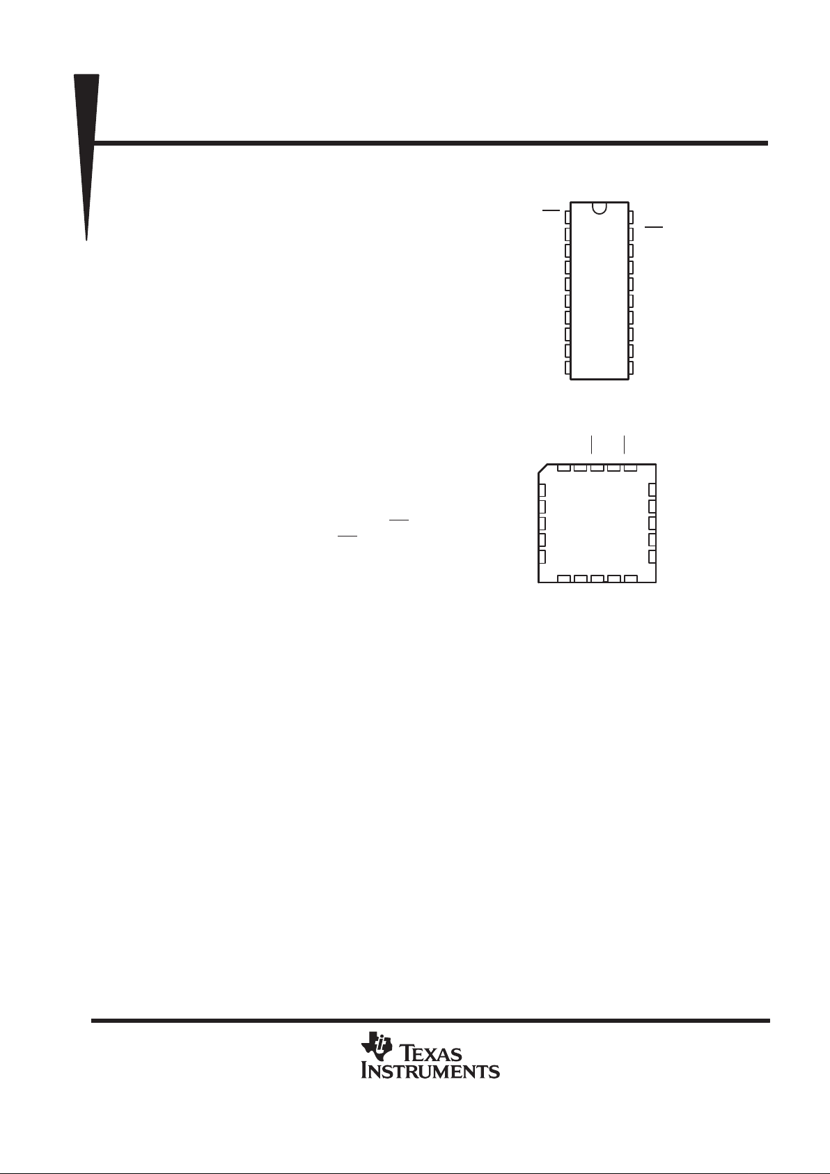
• Package Options Include Plastic
Small-Outline (DW) Packages, Ceramic
Chip Carriers (FK), and Standard Plastic (N)
and Ceramic (J) 300-mil DIPs
description
These octal buffers and line drivers are designed
specifically to improve both the performance and
density of 3-state memory address drivers, clock
drivers, and bus-oriented receivers and
transmitters by eliminating the need for 3-state
overlap protection. With the ′AS756 and
SN74AS757, these devices provide the choice of
selected combinations of inverting outputs,
symmetrical active-low output-enable (OE
)
inputs, and complementary OE and OE
inputs.
The SN54AS760 is characterized for operation
over the full military temperature range of –55°C
to 125°C. The SN74ALS760 and SN74AS760 are
characterized for operation from 0°C to 70°C.
1
2
3
4
5
6
7
8
9
10
20
19
18
17
16
15
14
13
12
11
1OE
1A1
2Y4
1A2
2Y3
1A3
2Y2
1A4
2Y1
GND
V
CC
2OE
1Y1
2A4
1Y2
2A3
1Y3
2A2
1Y4
2A1
SN54AS760 ...J PACKAGE
SN74ALS760, SN74AS760 . . . DW OR N PACKAGE
(TOP VIEW)
3 2 1 20 19
910111213
4
5
6
7
8
18
17
16
15
14
1Y1
2A4
1Y2
2A3
1Y3
1A2
2Y3
1A3
2Y2
1A4
SN54AS760 . . . FK PACKAGE
(TOP VIEW)
2Y4
1A1
1OE
1Y4
2A2 2OE
2Y1
GND
2A1
V
CC
PRODUCTION DATA information is current as of publication date.
Products conform to specifications per the terms of Texas Instruments
standard warranty. Production processing does not necessarily include
testing of all parameters.
SN54AS760, SN74ALS760, SN74AS760
OCTAL BUFFERS AND LINE DRIVERS
WITH OPEN-COLLECTOR OUTPUTS
SDAS141A – DECEMBER 1983 – REVISED JANUAR Y 1995
2
POST OFFICE BOX 655303 • DALLAS, TEXAS 75265
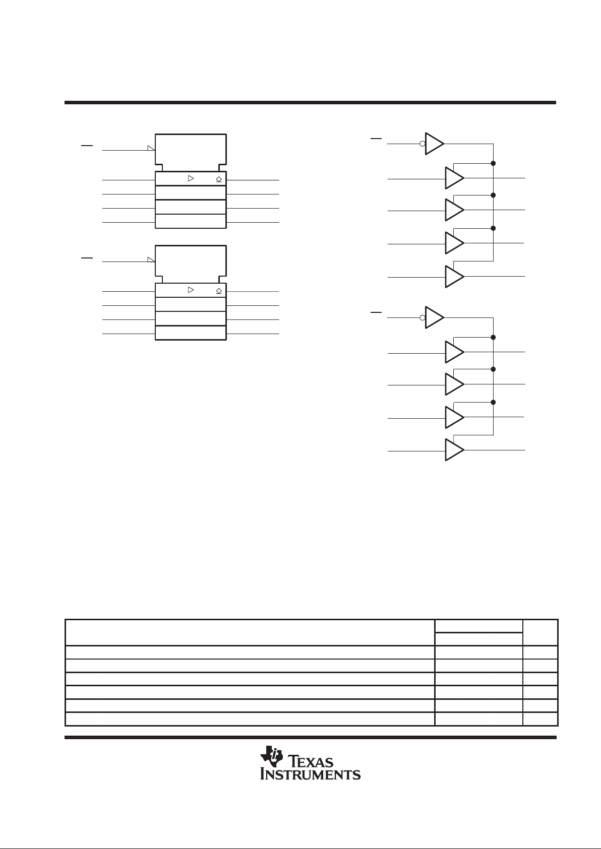
logic symbol
†
logic diagram (positive logic)
1
2
4
6
8
19
11
13
15
17
3
5
7
9
12
14
16
18
1A1
1A2
1A3
1A4
1Y1
2A1
2A2
2A3
2A4
2Y1
1Y2
1Y3
1Y4
2Y2
2Y3
2Y4
2OE
1OE
2
1A1
4
1A2
6
1A3
8
1A4
EN
1
1Y1
18
1Y2
16
1Y3
14
1Y4
12
11
2A1
13
2A2
15
2A3
17
2A4
EN
19
2Y1
9
2Y2
7
2Y3
5
2Y4
3
1OE
2OE
†
This symbol is in accordance with ANSI/IEEE Std 91-1984 and
IEC Publication 617-12.
absolute maximum ratings over operating free-air temperature range (unless otherwise noted)
‡
Supply voltage, V
CC
7 V. . . . . . . . . . . . . . . . . . . . . . . . . . . . . . . . . . . . . . . . . . . . . . . . . . . . . . . . . . . . . . . . . . . . . . . .
Input voltage, V
I
7 V. . . . . . . . . . . . . . . . . . . . . . . . . . . . . . . . . . . . . . . . . . . . . . . . . . . . . . . . . . . . . . . . . . . . . . . . . . . .
Off-state output voltage 7 V. . . . . . . . . . . . . . . . . . . . . . . . . . . . . . . . . . . . . . . . . . . . . . . . . . . . . . . . . . . . . . . . . . . . . .
Operating free-air temperature range, T
A
: SN74ALS760 0°C to 70°C. . . . . . . . . . . . . . . . . . . . . . . . . . . . . . . . .
Storage temperature range –65°C to 150°C. . . . . . . . . . . . . . . . . . . . . . . . . . . . . . . . . . . . . . . . . . . . . . . . . . . . . . .
‡
Stresses beyond those listed under “absolute maximum ratings” may cause permanent damage to the device. These are stress ratings only, and
functional operation of the device at these or any other conditions beyond those indicated under “recommended operating conditions” is not
implied. Exposure to absolute-maximum-rated conditions for extended periods may affect device reliability.
recommended operating conditions
SN74ALS760
MIN NOM MAX
UNIT
V
CC
Supply voltage 4.5 5 5.5 V
V
IH
High-level input voltage 2 V
V
IL
Low-level input voltage 0.8 V
V
OH
High-level output voltage 5.5 V
I
OL
Low-level output current 24 mA
T
A
Operating free-air temperature 0 70 °C
 Loading...