

Texas Instruments SN54ALS580BJ, SN74ALS580BDW, SN74ALS580BDWR, SN74ALS580BN, SN74ALS580BN3 Datasheet
...
SN54ALS580B, SN74ALS580B, SN74AS580
OCTAL D-TYPE TRANSPARENT LATCHES
WITH 3-STATE OUTPUTS
SDAS277 – JANUARY 1995
Copyright 1995, Texas Instruments Incorporated
1
POST OFFICE BOX 655303 • DALLAS, TEXAS 75265
• 3-State Buffer-Type Outputs Drive Bus
Lines Directly
• Bus-Structured Pinout
• Inverting-Logic Outputs
• Package Options Include Plastic
Small-Outline (DW) Packages, Ceramic
Chip Carriers (FK), Standard Plastic (N) and
Ceramic (J) 300-mil DIPs, and Ceramic Flat
(W) Packages
description
These octal D-type transparent latches feature
3-state outputs designed specifically for driving
highly capacitive or relatively low-impedance
loads. They are particularly suitable for
implementing buffer registers, I/O ports,
bidirectional bus drivers, and working registers.
While the latch-enable (LE) input is high, outputs
(Q
) respond to the data (D) inputs. When LE is low,
the outputs are latched to retain the data that was
set up.
A buffered output-enable (OE
) input can be used
to place the eight outputs in either a normal logic
state (high or low) or a high-impedance state. In
the high-impedance state, the outputs neither load
nor drive the bus lines significantly. The
high-impedance state and the increased drive
provide the capability to drive bus lines without
interface or pullup components.
OE
does not affect internal operations of the latches. Old data can be retained or new data can be entered while
the outputs are in the high-impedance state.
The SN54ALS580B is characterized for operation over the full military temperature range of –55°C to 125°C.
The SN74ALS580B and SN74AS580 are characterized for operation from 0°C to 70°C.
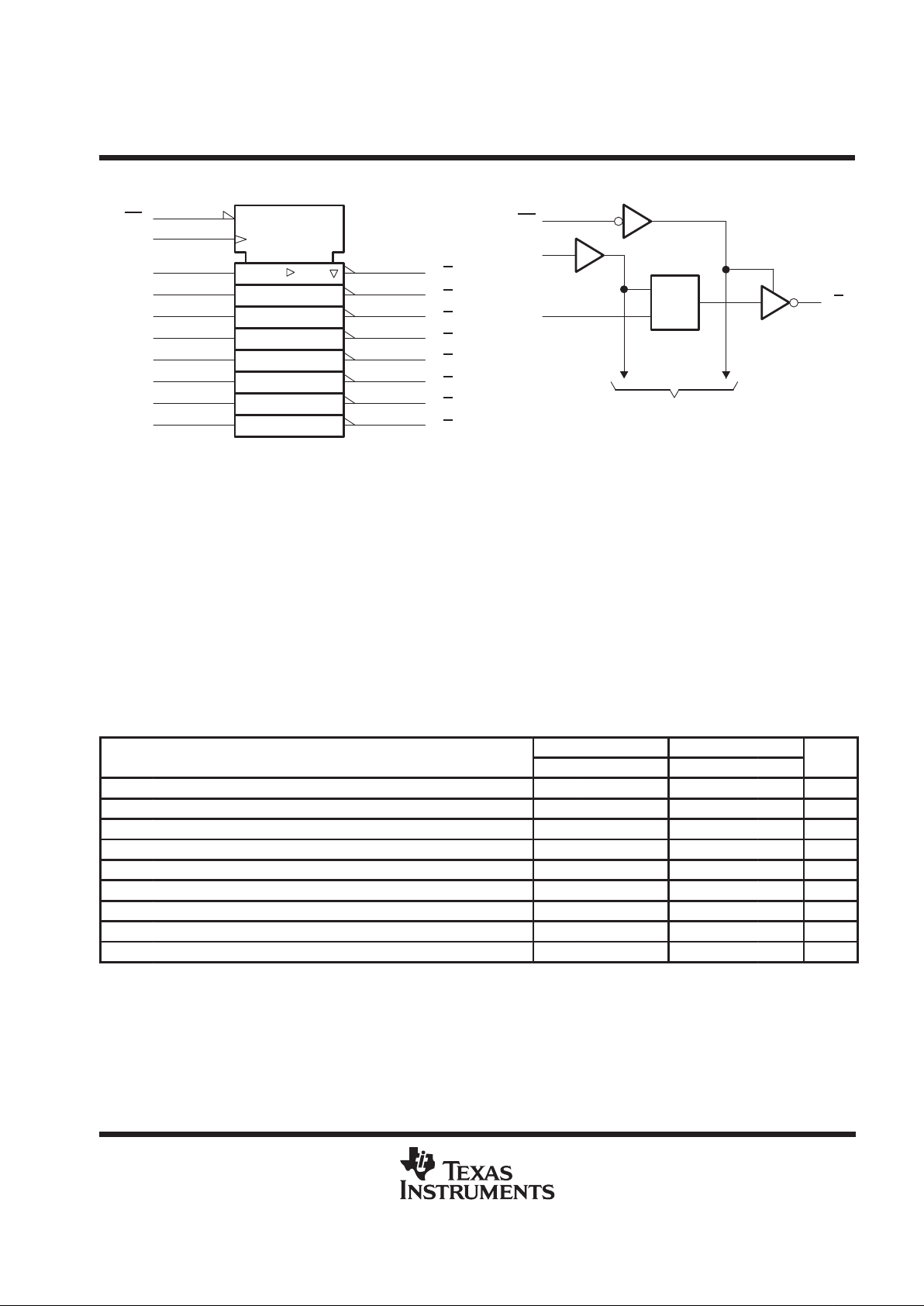
FUNCTION TABLE
(each latch)
INPUTS
OUTPUT
OE LE D
Q
L H H L
L HL H
LLX
Q
0
HXX Z
1
2
3
4
5
6
7
8
9
10
20
19
18
17
16
15
14
13
12
11
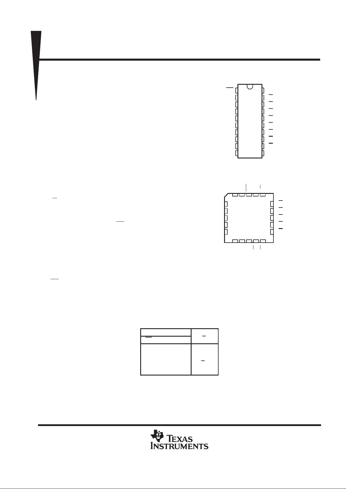
OE
1D
2D
3D
4D
5D
6D
7D
8D
GND
V
CC
1Q
2Q
3Q
4Q
5Q
6Q
7Q
8Q
LE
SN54ALS580B ...J OR W PACKAGE
SN74ALS580B, SN74AS580 . . . DW OR N PACKAGE
(TOP VIEW)
3212019
910111213
4
5
6
7
8
18
17
16
15
14
2Q
3Q
4Q
5Q
6Q
3D
4D
5D
6D
7D
SN54ALS580B . . . FK PACKAGE
(TOP VIEW)
2D1DOE
8Q
7Q 1Q
8D
GND
LE
V
CC
PRODUCTION DATA information is current as of publication date.
Products conform to specifications per the terms of Texas Instruments
standard warranty. Production processing does not necessarily include
testing of all parameters.
SN54ALS580B, SN74ALS580B, SN74AS580
OCTAL D-TYPE TRANSPARENT LATCHES
WITH 3-STATE OUTPUTS
SDAS277 – JANUARY 1995
2
POST OFFICE BOX 655303 • DALLAS, TEXAS 75265
logic symbol
†
logic diagram (positive logic)
OE
1D
2
1D
3
2D
4
3D
5
4D
6
5D
11
LE
19
18
17
16
15
14
13
12
7
6D
8
7D
9
8D
EN
1
OE
LE
1D
1Q
1
11
2
19
To Seven Other Channels
C1
1D
C1
1Q
2Q
3Q
4Q
5Q
6Q
7Q
8Q
†
This symbol is in accordance with ANSI/IEEE Std 91-1984 and
IEC Publication 617-12.
absolute maximum ratings over operating free-air temperature range (unless otherwise noted)
‡
Supply voltage, V
CC
7 V. . . . . . . . . . . . . . . . . . . . . . . . . . . . . . . . . . . . . . . . . . . . . . . . . . . . . . . . . . . . . . . . . . . . . . . .
Input voltage, V
I
7 V. . . . . . . . . . . . . . . . . . . . . . . . . . . . . . . . . . . . . . . . . . . . . . . . . . . . . . . . . . . . . . . . . . . . . . . . . . . .
Voltage applied to a disabled 3-state output 5.5 V. . . . . . . . . . . . . . . . . . . . . . . . . . . . . . . . . . . . . . . . . . . . . . . . . .
Operating free-air temperature range, T
A
: SN54ALS580B –55°C to 125°C. . . . . . . . . . . . . . . . . . . . . . . . . . .
SN74ALS580B 0°C to 70°C. . . . . . . . . . . . . . . . . . . . . . . . . . . . . . .
Storage temperature range –65°C to 150°C. . . . . . . . . . . . . . . . . . . . . . . . . . . . . . . . . . . . . . . . . . . . . . . . . . . . . . .
‡
Stresses beyond those listed under “absolute maximum ratings” may cause permanent damage to the device. These are stress ratings only, and
functional operation of the device at these or any other conditions beyond those indicated under “recommended operating conditions” is not
implied. Exposure to absolute-maximum-rated conditions for extended periods may affect device reliability.
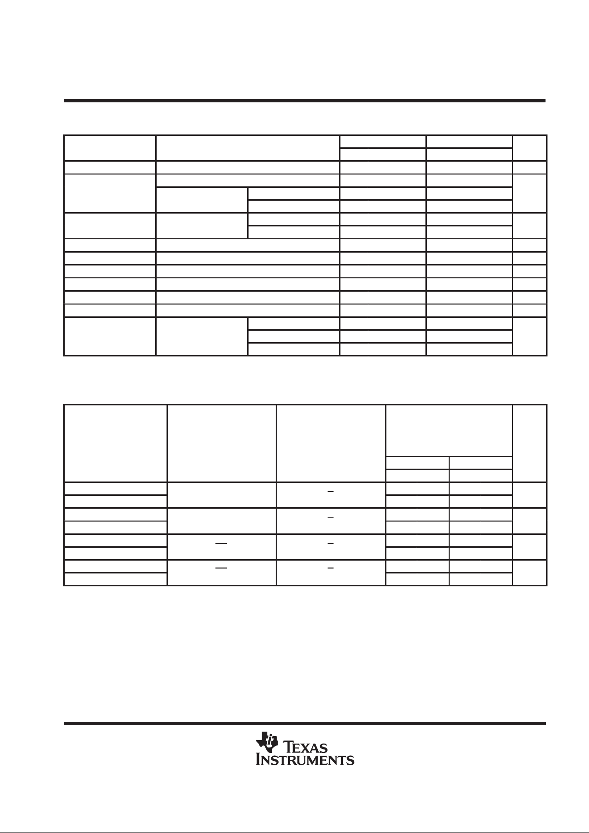
recommended operating conditions
SN54ALS580B SN74ALS580B
MIN NOM MAX MIN NOM MAX
UNIT
V
CC
Supply voltage 4.5 5 5.5 4.5 5 5.5 V
V
IH
High-level input voltage 2 2 V
V
IL
Low-level input voltage 0.7 0.8 V
I
OH
High-level output current –1 –2.6 mA
I
OL
Low-level output current 12 24 mA
t
w
Pulse duration, LE high 15 15 ns
t
su
Setup time, data before LE↓ 20 10 ns
t
h
Hold time, data after LE↓ 12 10 ns
T
A
Operating free-air temperature –55 125 0 70 °C
SN54ALS580B, SN74ALS580B, SN74AS580
OCTAL D-TYPE TRANSPARENT LATCHES
WITH 3-STATE OUTPUTS
SDAS277 – JANUARY 1995
3
POST OFFICE BOX 655303 • DALLAS, TEXAS 75265
electrical characteristics over recommended operating free-air temperature range (unless
otherwise noted)
SN54ALS580B SN74ALS580B
PARAMETER
TEST CONDITIONS
MIN TYP†MAX MIN TYP†MAX
UNIT
V
IK
VCC = 4.5 V, II = –18 mA –1.2 –1.2 V
VCC = 4.5 V to 5.5 V, IOH = –0.4 mA VCC –2 VCC –2
V
OH
IOH = –1 mA 2.4 3.3
V
V
CC
= 4.5
V
IOH = –2.6 mA 2.4 3.2
IOL = 12 mA 0.25 0.4 0.25 0.4
V
OL
V
CC
= 4.5
V
IOL = 24 mA 0.35 0.5
V
I
OZH
VCC = 5.5 V, VO = 2.7 V 20 20 µA
I
OZL
VCC = 5.5 V, VO = 0.4 V –20 –20 µA
I
I
VCC = 5.5 V, VI = 7 V 0.1 0.1 mA
I
IH
VCC = 5.5 V, VI = 2.7 V 20 20 µA
I
IL
VCC = 5.5 V, VI = 0.4 V –0.13 –0.1 mA
I
O
‡
VCC = 5.5 V, VO = 2.25 V –20 –112 –30 –112 mA
Outputs high 10 17 10 17
I
CC
VCC = 5.5 V
Outputs low 16 26 16 26
mA
Outputs disabled 17 29 17 29
†
All typical values are at VCC = 5 V, TA = 25°C.
‡
The output conditions have been chosen to produce a current that closely approximates one half of the true short-circuit output current, IOS.
switching characteristics (see Figure 1)
PARAMETER
FROM
(INPUT)
TO
(OUTPUT)
VCC = 4.5 V to 5.5 V,
CL = 50 pF,
R1 = 500 Ω
,
R2 = 500 Ω,
TA = MIN to MAX
§
UNIT
SN54ALS580B SN74ALS580B
MIN MAX MIN MAX
t
PLH
3 26 3 18
t
PHL
D
Q
3 15 3 14
ns
t
PLH
8 29 6 22
t
PHL
LE
Q
4 22 6 21
ns
t
PZH
4 25 3 18
t
PZL
OE
Q
4 21 4 18
ns
t
PHZ
2 12 1 10
t
PLZ
OE
Q
3 22 1 15
ns
§
For conditions shown as MIN or MAX, use the appropriate value specified under recommended operating conditions.
 Loading...