

Texas Instruments SN74AHCT125D, SN74AHCT125PWR, SN74AHCT125DBLE, SN74AHCT125DBR, SN74AHCT125DGVR Datasheet
...
SN54AHCT125, SN74AHCT125
QUADRUPLE BUS BUFFER GATES
WITH 3-STATE OUTPUTS
SCLS264L – DECEMBER 1995 – REVISED JANUARY 2000
D
EPIC
(Enhanced-Performance Implanted
CMOS) Process
D
Inputs Are TTL-Voltage Compatible
D
Latch-Up Performance Exceeds 250 mA Per
JESD 17
D
ESD Protection Exceeds 2000 V Per
MIL-STD-883, Method 3015
D
Package Options Include Plastic
Small-Outline (D), Shrink Small-Outline
(DB), Thin Very Small-Outline (DGV), Thin
Shrink Small-Outline (PW), and Ceramic
Flat (W) Packages, Ceramic Chip Carriers
(FK), and Standard Plastic (N) and Ceramic
(J) DIPs
description
The ’AHCT125 devices are quadruple bus buffer
gates featuring independent line drivers with
3-state outputs. Each output is disabled when the
associated output-enable (OE) input is high.
When OE
data from the A input to its Y output.
T o ensure the high-impedance state during power
up or power down, OE should be tied to V
through a pullup resistor; the minimum value of
the resistor is determined by the current-sinking
capability of the driver.
is low, the respective gate passes the
CC
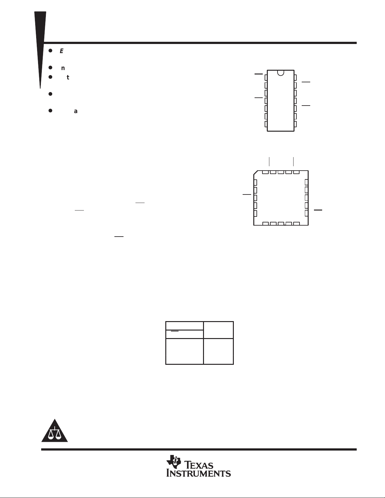
SN54AHCT125 ...J OR W PACKAGE
SN74AHCT125 . . . D, DB, DGV, N, OR PW PACKAGE
SN54AHCT125 . . . FK PACKAGE
1Y
NC
2OE
NC
2A
NC – No internal connection
(TOP VIEW)
1OE
1
1A
2
1Y
3
2OE
4
2A
5
6
2Y
GND
7
(TOP VIEW)
1A
3212019
4
5
6
7
8
910111213
2Y
1OE
GND
NC
NC
14
13
12
11
10
9
8
V
3Y
CC
V
CC
4OE
4A
4Y
3OE
3A
3Y
4OE
18
17
16
15
14
3A
4A
NC
4Y
NC
3OE
The SN54AHCT125 is characterized for
operation over the full military temperature range
of –55°C to 125°C. The SN74AHCT125 is
characterized for operation from –40°C to 85°C.
Please be aware that an important notice concerning availability, standard warranty, and use in critical applications of
Texas Instruments semiconductor products and disclaimers thereto appears at the end of this data sheet.
EPIC is a trademark of Texas Instruments Incorporated.
PRODUCTION DATA information is current as of publication date.
Products conform to specifications per the terms of Texas Instruments
standard warranty. Production processing does not necessarily include
testing of all parameters.
FUNCTION TABLE
(each buffer)
INPUTS
OE A
L H H
L LL
H X Z
OUTPUT
Y
Copyright 2000, Texas Instruments Incorporated
On products compliant to MIL-PRF-38535, all parameters are tested
unless otherwise noted. On all other products, production
processing does not necessarily include testing of all parameters.
POST OFFICE BOX 655303 • DALLAS, TEXAS 75265
1
SN54AHCT125, SN74AHCT125
QUADRUPLE BUS BUFFER GATES
WITH 3-STATE OUTPUTS
SCLS264L – DECEMBER 1995 – REVISED JANUARY 2000
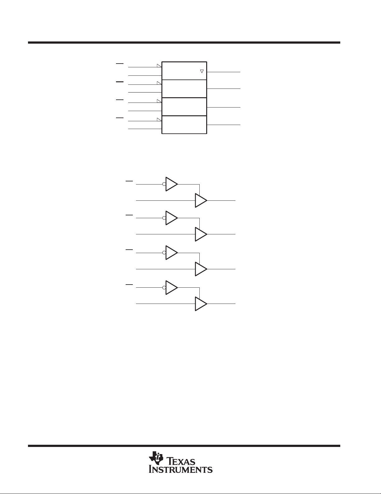
logic symbol
†
This symbol is in accordance with ANSI/IEEE Std 91-1984 and IEC Publication 617-12.
Pin numbers shown are for the D, DB, DGV, J, N, PW, and W packages.
†
1OE
1A
2OE
2A
3OE
3A
4OE
4A
1
2
4
5
10
9
13
12
EN
1
logic diagram (positive logic)
1
1OE
2
1A 1Y
4
2OE
5
2A 2Y
3
1Y
6
2Y
8
3Y
11
4Y
3
6
10
3OE
9
3A 3Y
13
4OE
12
4A 4Y
Pin numbers shown are for the D, DB, DGV, J, N, PW, and W packages.
8
11
2
POST OFFICE BOX 655303 • DALLAS, TEXAS 75265
 Loading...